Order
Now
Product
Folder
Support &
Community
Tools &
Software
Technical
Documents
TCA4311A
SCPS226C – JANUARY 2011 – REVISED AUGUST 2018
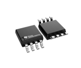
TCA4311A Hot Swappable 2-Wire Bus Buffers
1 Features
3 Description
•
The TCA4311A is a hot-swappable I2C bus buffer
that supports I/O card insertion into a live backplane
without corruption of the data and clock busses.
Control circuitry prevents the backplane from being
connected to the card until a stop command or bus
idle occurs on the backplane without bus contention
on the card. When the connection is made, this
device provides bidirectional buffering, keeping the
backplane and card capacitances isolated. During
insertion, the SDA and SCL lines are pre-charged to
1 V to minimize the current required to charge the
parasitic capacitance of the chip.
1
•
•
•
•
•
•
•
•
•
•
•
•
•
•
Operating Power-Supply Voltage Range of 2.7 V
to 5.5 V
Supports Bidirectional Data Transfer of I2C Bus
Signals
SDA and SCL Lines are Buffered Which Increases
Fanout
1-V Precharge on all SDA and SCL Lines
Prevents Corruption During Live Board Insertion
and Removal From Backplane
SDA and SCL Input Lines are Isolated From
Outputs
Accommodates Standard Mode and Fast Mode
I2C Devices
Improved Noise Immunity
Applications Include Hot Board Insertion and Bus
Extension
Low ICC Chip Disable of < 1 μA
READY Open-Drain Output
Supports Clock Stretching, Arbitration, and
Synchronization
Powered-Off High-Impedance I2C Pins
Open-Drain I2C Pins
Latch-Up Performance Exceeds 100 mA Per
JESD 78, Class II
ESD Protection Exceeds JESD 22
– 8000-V Human-Body Model (A114-A)
– 200-V Machine Model (A115-A)
– 1000-V Charged-Device Model (C101)
When the I2C bus is idle, the TCA4311A can be put
into shutdown mode by setting the EN pin low. When
EN is high, the TCA4311A resumes normal operation.
It also includes an open drain READY output pin,
which indicates that the backplane and card sides are
connected together. When READY is high, the
SDAIN and SCLIN are connected to SDAOUT and
SCLOUT. When the two sides are disconnected,
READY is low.
Both the backplane and card may be powered with
supply voltages ranging from 2.7 V to 5.5 V, with no
restrictions on which supply voltage is higher.
The TCA4311A has standard open-drain I/Os. The
size of the pull-up resistors to the I/Os depends on
the system, but each side of this buffer must have a
pull-up resistor. The device is designed to work with
Standard Mode and Fast Mode I2C devices in
addition to SMBus devices. Standard Mode I2C
devices only specify 3 mA in a generic I2C system
where Standard Mode devices and multiple masters
are possible. Under certain conditions, high
termination currents can be used.
2 Applications
•
•
•
•
Device Information(1)
Servers
Routers (Telecom Switching Equipment)
Base Stations
Industrial Automation
PART NUMBER
TCA4311A
PACKAGE
BODY SIZE (NOM)
SOIC (8)
4.90 mm × 3.91 mm
VSSOP (8)
3.00 mm × 3.00 mm
(1) For all available packages, see the orderable addendum at
the end of the datasheet.
Simplified Schematic
VCC
SDAIN
SCLIN
SDAOUT
SCLOUT
Add-on card
2
I C bus or SMBus
2
Backplane I C
bus or SMBus
TCA4311A
EN
READY
GND
1
An IMPORTANT NOTICE at the end of this data sheet addresses availability, warranty, changes, use in safety-critical applications,
intellectual property matters and other important disclaimers. PRODUCTION DATA.
�TCA4311A
SCPS226C – JANUARY 2011 – REVISED AUGUST 2018
www.ti.com
Table of Contents
1
2
3
4
5
6
7
8
Features ..................................................................
Applications ...........................................................
Description .............................................................
Revision History.....................................................
Pin Configuration and Functions .........................
Specifications.........................................................
1
1
1
2
3
4
6.1
6.2
6.3
6.4
6.5
6.6
4
4
4
4
5
6
Absolute Maximum Ratings .....................................
ESD Ratings..............................................................
Recommended Operating Conditions.......................
Thermal Information ..................................................
Electrical Characteristics ..........................................
Typical Characteristics ..............................................
Parameter Measurement Information .................. 6
Detailed Description .............................................. 8
8.1 Overview ................................................................... 8
8.2 Functional Block Diagram ......................................... 8
8.3 Feature Description................................................... 9
8.4 Device Functional Modes.......................................... 9
9
Application and Implementation ........................ 11
9.1 Application Information............................................ 11
9.2 Typical Application .................................................. 11
10 Power Supply Recommendations ..................... 17
11 Layout................................................................... 17
11.1 Layout Guidelines ................................................. 17
11.2 Layout Example .................................................... 18
12 Device and Documentation Support ................. 19
12.1
12.2
12.3
12.4
12.5
Receiving Notification of Documentation Updates
Community Resources..........................................
Trademarks ...........................................................
Electrostatic Discharge Caution ............................
Glossary ................................................................
19
19
19
19
19
13 Mechanical, Packaging, and Orderable
Information ........................................................... 19
4 Revision History
Changes from Revision B (October 2014) to Revision C
Page
•
Moved Tstg to the Absolute Maximum Rating table ................................................................................................................ 4
•
Changed the Handling Rating table To: ESD Ratings ........................................................................................................... 4
•
Added Missing ACK Event section ....................................................................................................................................... 10
Changes from Revision A (July 2012) to Revision B
Page
•
Handling Rating table, Feature Description section, Device Functional Modes, Application and Implementation
section, Power Supply Recommendations section, Layout section, Device and Documentation Support section, and
Mechanical, Packaging, and Orderable Information section. ................................................................................................ 1
•
Changed the TCA4311A RTA Specification. ......................................................................................................................... 1
Changes from Original (January 2011) to Revision A
•
2
Page
Updated Input-output Offset Voltage vs Pullup Resistor graphic. .......................................................................................... 6
Submit Documentation Feedback
Copyright © 2011–2018, Texas Instruments Incorporated
Product Folder Links: TCA4311A
�TCA4311A
www.ti.com
SCPS226C – JANUARY 2011 – REVISED AUGUST 2018
5 Pin Configuration and Functions
D OR DGK Packages
(Top View)
Pin Functions
PIN
NAME
DESCRIPTION
NUMBER
EN
1
Active-high chip enable pin. If EN is low, the TCA4311A is in a low current (
很抱歉,暂时无法提供与“TCA4311ADGKR”相匹配的价格&库存,您可以联系我们找货
免费人工找货- 国内价格 香港价格
- 1+26.197671+3.27366
- 10+19.5738310+2.44594
- 25+17.9143625+2.23858
- 100+16.09541100+2.01128
- 250+15.22736250+1.90281
- 500+14.70436500+1.83746
- 1000+14.273861000+1.78366
- 国内价格
- 1+5.18670
- 10+4.71520
- 100+4.36590
- 500+4.15800
- 1000+3.96010
- 国内价格
- 1+5.70240
- 10+4.53600
- 30+3.95280
- 100+3.34660
- 500+3.00446
- 1000+2.82269
