User's Guide
SLVUA91 – July 2014
TCA5013EVM
This document is the user’s guide for the TCA5013 Evaluation Module (TCA5013EVM). The
TCA5013EVM allows for evaluation of the TCA5013 smart card interface integrated circuit (IC) for one
user card and three SAMs. This guide contains an introduction, setup instructions, the EVM schematic,
top and bottom board layouts and component views, internal VDD and GND plane layouts, and a bill of
materials.
1
2
3
4
5
6
7
Contents
Information About Cautions and Warnings ............................................................................... 2
Items Required for Operation .............................................................................................. 2
Introduction ................................................................................................................... 3
Setup .......................................................................................................................... 5
4.1
Header, Jumper, and Test Point Descriptions .................................................................. 5
4.2
Getting Started Using the TCA5013EVM ........................................................................ 8
Schematic ................................................................................................................... 12
Board Layout ................................................................................................................ 13
Bill of Materials ............................................................................................................. 19
List of Figures
1
TCA5013EVM ................................................................................................................ 4
2
TCA5013EVM Schematic ................................................................................................. 12
3
PCB Layer 1 (Top Layer).................................................................................................. 13
4
PCB Layer 1 (Component View) ......................................................................................... 14
5
PCB Layer 2 (VDD Plane)
6
PCB Layer 3 (GND Plane) ................................................................................................ 16
7
PCB Layer 4 (Bottom Layer) .............................................................................................. 17
8
PCB Layer 4 (Component View) ......................................................................................... 18
1
Device and Package Configurations ...................................................................................... 3
2
TCA5013 Register Map ..................................................................................................... 9
3
Bill of Materials
................................................................................................
15
List of Tables
.............................................................................................................
SLVUA91 – July 2014
Submit Documentation Feedback
TCA5013EVM
Copyright © 2014, Texas Instruments Incorporated
19
1
�Information About Cautions and Warnings
1
www.ti.com
Information About Cautions and Warnings
The information in a caution or a warning is provided for your protection. Read each caution and warning
carefully.
CAUTION
This EVM contains components that can potentially be damaged by
electrostatic discharge. Always transport and store the EVM in its supplied ESD
bag when not in use. Handle using an antistatic wristband. Operate on an
antistatic work surface. For more information on proper handling, see the
Electrostic Discharge (ESD) application note (SSYA008).
2
Items Required for Operation
The following items are required to use the TCA5013EVM:
• TCA5013 datasheet (SCPS253)
• TCA5013EVM
• Power supply, or MSP430 LaunchPad™ to supply power
• Clock source, or MSP430 LaunchPad to apply a clock signal
• Digital logic, or MSP430 LaunchPad to apply A0, SHDN, and/or IO signals
The following items are recommended for developing firmware for an attached processor to control the
TCA5013EVM:
• MSP-EXP430G2 LaunchPad
– Recommended rev 1.5
– MSP430G2553 installed
• or MSP-EXP430F5529LP LaunchPad
• USB standard-A to mini-B cable
• Computer with Code Composer Studio installed
• Firmware/software and installation guide (SLVC581)
LaunchPad is a trademark of Texas Instruments.
2
TCA5013EVM
SLVUA91 – July 2014
Submit Documentation Feedback
Copyright © 2014, Texas Instruments Incorporated
�Introduction
www.ti.com
3
Introduction
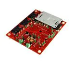
The TCA5013EVM allows a simple way to evaluate the TCA5013 with an MSP-EXP430G2 LaunchPad,
MSP-EXP430F5529LP LaunchPad, or other processor. The TCA5013EVM is built with one user card slot
which allows the TCA5013 to detect the insertion and removal of the user card. The user card, also known
as an IC card, contains the account information for the consumer using an electronic point of sale (ePOS)
terminal. The TCA5013EVM is also built with three Secure Access Module (SAM) card cages. A SAM card
physically resembles a Subscriber Identification Module (SIM) but contains information relevant to an
ePOS transaction. Although the TCA5013 is not a full ePOS system, it allows the user to evaluate the
TCA5013 IC and provides a foundation for developing firmware to control the TCA5013 and communicate
with a user card and up to three SAM cards.
Table 1. Device and Package Configurations
IO Expander
IC
Package
U1
TCA5013ZAH
BGA-48
SLVUA91 – July 2014
Submit Documentation Feedback
TCA5013EVM
Copyright © 2014, Texas Instruments Incorporated
3
�Introduction
www.ti.com
Figure 1. TCA5013EVM
4
TCA5013EVM
SLVUA91 – July 2014
Submit Documentation Feedback
Copyright © 2014, Texas Instruments Incorporated
�Setup
www.ti.com
4
Setup
This section describes the header/jumper connections on the EVM and getting started using the
TCA5013EVM.
4.1
Header, Jumper, and Test Point Descriptions
The headers, jumpers, and test points are listed in the order they can be found on the PCB, from top left
to bottom right, across then down. However, related jumpers/headers/test points are listed simultaneously.
4.1.1
GND: Signal Ground
Test points labeled GND are connected to signal ground, which is also connected to the GND pins of the
TCA5013. There are five test points spread out across the board for easy attachment of oscilloscope
ground connections. They are all connected directly to the signal ground plane.
4.1.2
J_UC, J_S3, J_S2, and J_S1: Card Slot and Card Cages
Card slot J_UC is where the user card is inserted into the TCA5013EVM. Card cages J_S1, J_S2, and
J_S3 are where SAM1, SAM2, and SAM3 cards are inserted into the TCA5013EVM.
4.1.3
JIO_S3, JIO_S2, JIO_S1, and JIO_UC: IO Pins, Card Side
Headers JIO_UC, JIO_S1, JIO_S2, and JIO_S3 are respectively connected to IOUC, IOS1, IOS2, and
IOS3 of the TCA5013 IC. These headers are test points for the IO signal which is routed to the associated
card slot or card cage.
4.1.4
JT1, JT2, JT3, and JT4: Test Pins
Jumpers JT1, JT2, JT3, and JT4 are respectively connected from pin 2 to pins TST1, TST2, TST3, and
TST4 on the TCA5013 IC. Pin 1 of these jumpers is connected to GND. These pins are grounded in
practice; therefore, the jumper connection needs to be installed to ensure proper operation of the
TCA5013.
4.1.5
JRST_S3, JRST_S2, JRST_S1, and JRST_UC: Reset Pins at Cards
Headers JRST_UC, JRST_S1, JRST_S2, and JRST_S3 are respectively connected to RSTUC, RSTS1,
RSTS2, and RSTS3 of the TCA5013 IC. These headers are test points for the RST signal which is routed
to the associated card slot or card cage.
4.1.6
JU_A0: Address PIn
Jumper JU_A0 is connected via the center pin (pin 2) to A0 of the TCA5013 IC. When pins 1 and 2 are
connected with a jumper, A0 is connected to GND through a weak pull-down resistor. When pins 2 and 3
are connected with a jumper, A0 is connected to VDDI through a weak pull-down resistor. Pin 2 is also
routed to pin 3 of receptacle J2.
4.1.7
JCLK_S3, JCLK_S2, JCLK_S1, JCLK_UC: Clock Pins, Card Side
Headers JCLK_UC, JCLK_S1, JCLK_S2, and JCLK_S3 are respectively connected to CLKUC, CLKS1,
CLKS2, and CLKS3 of the TCA5013 IC. These headers are test points for the CLK signal which is routed
to the associated card slot or card cage.
4.1.8
JU_SHDN: Shutdown Pin
Jumper JU_SHDN is connected via the center pin (pin 2) to SHDN of the TCA5013 IC. When pins 1 and 2
are connected with a jumper, SHDN is connected to GND through a weak pull-down resistor. When pins 2
and 3 are connected with a jumper, SHDN is connected to VDDI through a weak pull-up resistor. Pin 2 is
also routed to pin 7 of receptacle J1.
SLVUA91 – July 2014
Submit Documentation Feedback
TCA5013EVM
Copyright © 2014, Texas Instruments Incorporated
5
�Setup
4.1.9
www.ti.com
TPVCC(S3), TPVCC(S2), TPVCC(S1), TPVCC_UC: VCC Pins at Cards
Test points TPVCC(UC), TPVCC(S1), TPVCC(S2), and TPVCC(S3) are respectively connected to
VCCUC, VCCS1, VCCS2, and VCCS3 of the TCA5013 IC. These test points can be used to probe the
voltage on VCC, the power supply to the associated card.
4.1.10
JU_PRES_NO, JU_PRES_NC, and TPPRES: PRES Pin Jumpers and Test Points
Jumpers JU_PRES_NO and JU_PRES_NC are both connected by the center pin (pin 2) to the PRES pin
of the TCA5013 IC. These jumpers can be used to configure whether a user card inserted in the slot
results in a logic HI to LO transition or a LO to HI transition. Connecting pin 2 of JU_PRES_NC to VDDI
and connecting pin 2 of JU_PRES_NO to GND means that PRES is normally connected to VDDI and
inserting a card results in a HI to LO transition. Conversely, connecting pin 2 of JU_PRES_NC to GND
and connecting pin 2 of JU_PRES_NO to VDDI means that PRES is normally connected to GND and
inserting a card results in a LO to HI transition.
Test point TPPRES is connected to the PRES pin of the TCA5013 IC and can be used to probe the
voltage on this pin when a card is inserted or removed from the card slot.
4.1.11
TPC4 and TPC8: C4 and C8 Pins at User Card
Test points TPC4 and TPC8 are respectively connected to pins C4 and C8 of the TCA5013 IC. These test
points can be used to probe the C4 or C8 signal routed to the user card.
4.1.12
TP3VDDI, TP2VDDI, TPVDDI: VDDI Pin Test Points
Test points TPV1DDI, TP2VDDI, and TP3VDDI are all connected directly to the VDDI plane and can be
used to probe the power supply to the VDDI pin of the TCA5013 IC.
4.1.13
TPG4, TPG3, TPG2, and TPG1: GPIO Pins
Test points TPG1, TPG2, TPG3, and TPG4 are respectively connected to the GPIO1, GPIO2, GPIO3, and
GPIO4 pins of the TCA5013 IC. These test points can be used to probe the output voltage of the GPIO
pins or apply an input voltage to the GPIO pins.
4.1.14
TPVUP and TPLX: VUP and LX Pins
Test points TPVUP and TPLX are respectively connected to the VUP and LX pins of the TCA5013 and
can be used to probe the boost circuitry of the device.
4.1.15
GNDP: Power Ground
Test point GNDP is connected to power ground plane and the GNDP pin of the TCA5013 IC, which is
separated from the signal ground plane with a 0.003Ω resistor.
4.1.16
TPCLKIN2 and TPCLKIN1: CLK Pins, Host Side
Test points TPCLKIN1 and TPCLKIN2 are respectively connected to the CLKIN1 and CLKIN2 pins of the
TCA5013 IC. These test points can be used to probe the clock signals at the host side of the TCA5013.
4.1.17
TP2VDD and TP1VDD: VDD Pin Test Point
Test points TP1VDD and TP2VDD are both connected directly to the VDD plane and can be used to
probe the power supply to the VDD pin of the TCA5013 IC.
4.1.18
JU_IOUCA and JU_IOUCB: IO Pins, Host Side
Jumpers JU_IOUCA and JU_IOUCB are both connected to IOMC1 at pin 1 and to IOMC2 at pin 2. If
either one of the headers has pin 1 and pin 2 connected with a jumper, then IOMC1 and IOMC2 are
shorted together. The pins of these headers can also be used as test points to probe the IO signals on the
host side of the TCA5013 IC.
6
TCA5013EVM
SLVUA91 – July 2014
Submit Documentation Feedback
Copyright © 2014, Texas Instruments Incorporated
�Setup
www.ti.com
4.1.19
TPSCL and TPSDA: I2C Communication Pins
Test points TPSCL and TPSDA are respectively connected to the SCL and SDA pins of the TCA5013 IC.
SCL and SDA are the signal names for the 2-wire I2C communication protocol, which is used to control
and communicate with the TCA5013. These test points can be used to probe SCL and SDA to interpret
I2C communication from the processor to the TCA5013.
4.1.20
JU_CLKIN2 and JU_CLKIN1: CLKIN1 and CLKIN2 Jumpers
Jumpers JU_CLKIN1 and JU_CLKIN2 are respectively connected from the center pin, labeled CLKIN1
and CLKIN2, to the CLKIN1 and CLKIN2 pins of the TCA5013 IC. Connecting CLKIN1 (or CLKIN2) to
MSP allows an attached MSP430 processor to supply a clock to the CLKIN1 (or CLKIN2) pin of the
TCA5013. Connecting CLKIN1 (or CLKIN2) to EXT1 (or EXT2) allows a clock signal to be applied to the
TCA5013 via the S1 (or S2) SMB connector.
4.1.21
J1 and J2: MSP-EXP430G2 Connection Receptacles
Receptacles J1 and J2 allow the TCA5013EVM to interface with an MSP-EXP430G2 LaunchPad. See the
TCA5013EVM schematic in Figure 2 to determine which signals from the LaunchPad are connected to the
TCA5013.
4.1.22
J3 and J4: MSP-EXP430F5529LP Additional Connection Receptacles
Receptacles J3 and J4, in conjunction with headers J1 and J2, allow the TCA5013EVM to interface with
an MSP-EXP430F5529LP LaunchPad. See the TCA5013EVM schematic in Figure 2 to determine which
signals from the LaunchPad are connected to the TCA5013.
4.1.23
S2 and S1: SMB Connections for Clock Source
SMB connectors S1 and S2 allow a clock signal to be externally applied to the respective CLKIN1 and
CLKIN2 pins of the TCA5013 IC. There is a 50-Ω termination resistance, RT1 (and RT2), between S1 and
JU_CLKIN1 (and between S2 and JU_CLKIN2) which can be removed if the external clock applied does
not have a matched 50-Ω resistance.
4.1.24
TPRST: RST Pin for MSP430 LaunchPad
Test point TPRST connects to the RST pin of the LaunchPad and can be used to manually reset the
MSP430 processor.
4.1.25
JU_VDDI and JVDDI: VDDI Power Supply Pin Connections
Jumper JU_VDDI is connected via the center pin, labeled VDDI, to VDDI of the TCA5013 IC. Connecting
VDDI to 3V6 allows the LaunchPad to supply power VDDI of the TCA5013. Connecting VDDI to EXT
allows power to be applied externally.
Screw terminal JVDDI can be used to supply power to the EXT pin of JU_VDDI from an external power
supply.
4.1.26
JU_VDD and JVDD: VDD Power Supply Pin Connections
Jumper JU_VDD is connected via the center pin, labeled VDD, to VDD of the TCA5013 IC. Connecting
VDD to 3V6 allows the LaunchPad to supply power VDD of the TCA5013. Connecting VDD to EXT allows
power to be applied externally.
Screw terminal JVDD can be used to supply power to the EXT pin of JU_VDD from an external power
supply.
4.1.27
TP(Vdd_MSP): Test Point for MSP430 LaunchPad Power Supply
Test point TP(Vdd_MSP) is connected to the power supply rail of the LaunchPad and can be used to
probe the voltage supplied by the LaunchPad, which is nominally 3.6 V.
SLVUA91 – July 2014
Submit Documentation Feedback
TCA5013EVM
Copyright © 2014, Texas Instruments Incorporated
7
�Setup
4.2
4.2.1
www.ti.com
Getting Started Using the TCA5013EVM
MSP-EXP430G2 LaunchPad Setup
If the TCA5013EVM is to be used in conjunction with the MSP-EXP430G2 LaunchPad, the LaunchPad
can supply power and provide all of the signals necessary to communicate with the user card and SAM
cards.
Prior to setup, ensure the LaunchPad is not plugged into a computer.
To begin the setup, the TCA5013EVM J1 and J2 receptacles must be connected to the J1 and J2 headers
on the LaunchPad. For the LaunchPad to provide the A0 and SHDN signals to the TCA5013, it is
recommended that the shunt on JU_A0 and JU_SHDN be removed. For the LaunchPad to provide the IO
signals to communicate with the user card and SAM cards through the TCA5013, either JU_IOUCA or
JU_IOUCB must have a shunt connecting the pins labeled IOUC1 and IOUC2. If both of these shunts are
removed, the LaunchPad can only communicate with the SAM cards. For the LaunchPad to provide the
CLK signal to the card through the TCA5013, JU_CLKIN1 and JU_CLKIN2 must have a shunt connected
from the pin labeled CLKIN1 to MSP and CLKIN2 to MSP. Finally, for the LaunchPad to supply power to
the TCA5013 and thereby supply power to the user card and SAM cards with the boost circuitry and
integrated LDOs, JU_VDD and JU_VDDI must be connected from the pin labeled VDD to 3V6 and VDDI
to 3V6.
Optionally, any of these power supplies or signals can be provided externally by following the alternate
descriptions in Section 4.1.
After this setup is complete, the LaunchPad may be plugged into a computer by a USB standard-A to
mini-B cable.
4.2.2
Using the Sample MSP-EXP430G2 Firmware/Software
The sample firmware/software for the MSP-EXP430G2 LaunchPad provides a simple way to control the
TCA5013 and demonstrate its functionality. Using a computer as an interface, all of the registers can be
read from and written to individually. Core features, such as card activation, that involve writing to multiple
registers are performed simultaneously by the processor. In addition, the processor also provides a simple
interrupt handling routine. The sample code, detailed installation instructions, and hardware setup
information can be found in the zipped folder SLVC581, TCA5013EVM Software/Firmware Package, and
will be updated as bug fixes and enhanced features become available.
8
TCA5013EVM
SLVUA91 – July 2014
Submit Documentation Feedback
Copyright © 2014, Texas Instruments Incorporated
�Setup
www.ti.com
4.2.3
TCA5013 Register Map Overview
A detailed description of the TCA5013 register map can be found in the datasheet. As a reference, an overview of the register map is shown in
Table 2.
Table 2. TCA5013 Register Map
Type
User
Card
Address
(Hex)
Register
Description
Type
Reset
(Hex)
Reset
(Binary)
Bit 7
Bit 6
Bit 5
Bit 4
Bit 3
R
00
0000 0000
ACTIVE_UC
EARLY_UC
MUTE_UC
PROT_UC
Bit 2
Bit 1
CLKSW_UC
PRESL_UC
PRES_UC
IO_EN_UC
WARM_UC
CARD_DETECT_
UC
CLK1_UC
CLK_DIV_UC
00
User Card Slot
Status
01
User Card Slot
Settings
R/W
60
0110 0000
02
User Card
Clock Settings
R/W
0C
0000 1100
03
Asynchronous
Mode ATR
EARLY
counter MSB
for User Card
R/W
AA
1010 1010
04
Asynchronous
Mode ATR
EARLY
counter LSB
for User Card
R/W
00
0000 0000
05
Asynchronous
Mode ATR
MUTE counter
MSB for User
Card
R/W
A4
1010 0100
MUTE_COUNT_HI_UC
06
Asynchronous
Mode ATR
MUTE counter
LSB for User
Card
R/W
74
0111 0100
MUTE_COUNT_LO_UC
07
User Card IO
Slew Rate
Settings
R/W
80
1000 0000
08
User Card
Clock Slew
Rate Settings
R/W
A0
1010 0000
09
User Card
Synchronous
Mode Settings
R/W
76
0111 0110
0A
Synchronous
Mode ATR
Byte 1
R
00
0000 0000
BYTE1_UC
0B
Synchronous
Mode ATR
Byte 2
R
00
0000 0000
BYTE2_UC
0C
Synchronous
Mode ATR
Byte 3
R
00
0000 0000
BYTE3_UC
0D
Synchronous
Mode ATR
Byte 4
R
00
0000 0000
BYTE4_UC
SET_VCC_UC
INTERN_CLK _UC
CLK0_UC
Bit 0
VCC_FAIL_UC
START_ASYNC_
UC
EARLY_COUNT_HI_UC
EARLY_COUNT_LO_UC
IO_TR_UC
IO_TF_UC
CLK_SR_UC
CARD_TYPE
ACTIVATION_
TYPE
C4
C8
SLVUA91 – July 2014
Submit Documentation Feedback
RST
CLK_ENABLE_
SYNC
EDGE
START_SYNC
TCA5013EVM
Copyright © 2014, Texas Instruments Incorporated
9
�Setup
www.ti.com
Table 2. TCA5013 Register Map (continued)
Type
Address
(Hex)
Reset
(Hex)
Reset
(Binary)
Bit 7
Bit 6
Bit 5
Bit 4
Bit 3
Bit 2
Bit 1
Bit 0
ACTIVE_SAM1
EARLY_SAM1
MUTE_SAM1
PROT_SAM1
CLKSW_SAM1
STAT_OTP
STAT_SUPL
VCC_FAIL_
SAM1
SAM1 Slot
Status
R
00
0000 0000
11
SAM1 Slot
Settings
R/W
40
0100 0000
12
SAM1 Clock
Settings
R/W
0C
0000 1100
13
Asynchronous
Mode ATR
EARLY
counter MSB
for SAM1
R/W
AA
1010 1010
14
Asynchronous
Mode ATR
EARLY
counter LSB
for SAM1
R/W
00
0000 0000
15
Asynchronous
Mode ATR
MUTE counter
MSB for SAM1
R/W
A4
1010 0100
MUTE_COUNT_HI_SAM1
16
Asynchronous
Mode ATR
MUTE counter
LSB for SAM1
R/W
74
0111 0100
MUTE_COUNT_LO_SAM1
17
SAM IO Slew
Rate Settings
R/W
80
1000 0000
18
SAM Clock
Slew Rate
Settings
R/W
A0
1010 0000
20
SAM2 Slot
Status
R
00
0000 0000
21
SAM2 Slot
Settings
R/W
40
0100 0000
22
SAM2 Clock
Settings
R/W
0C
0000 1100
23
Asynchronous
Mode ATR
EARLY
counter MSB
for SAM2
R/W
AA
1010 1010
24
Asynchronous
Mode ATR
EARLY
counter LSB
for SAM2
R/W
00
0000 0000
25
Asynchronous
Mode ATR
MUTE counter
MSB for SAM2
R/W
A4
1010 0100
MUTE_COUNT_HI_SAM2
26
Asynchronous
Mode ATR
MUTE counter
LSB for SAM2
R/W
74
0111 0100
MUTE_COUNT_LO_SAM2
SAM2
10
Type
10
SAM1
SAM
1-3
Slew
Rates
Register
Description
SET_VCC_SAM1
INTERN_CLK_
SAM1
CLK0_SAM1
IO_EN_SAM1
WARM_SAM1
CLK1_SAM1
CLK_DIV_SAM1
START_ASYNC_
SAM1
EARLY_COUNT_HI_SAM1
EARLY_COUNT_LO_SAM1
IO_TR_SAM
IO_TF_SAM
CLK_SR_SAM
ACTIVE_SAM2
MUTE_SAM2
SET_VCC_SAM2
INTERN_CLK_
SAM2
CLK0_SAM2
PROT_SAM2
CLKSW_SAM2
VCC_FAIL_SAM2
IO_EN_SAM2
WARM_SAM2
CLK1_SAM2
CLK_DIV_SAM2
START_ASYNC_
SAM2
EARLY_COUNT_HI_SAM2
EARLY_COUN_LO_SAM2
TCA5013EVM
SLVUA91 – July 2014
Submit Documentation Feedback
Copyright © 2014, Texas Instruments Incorporated
�Setup
www.ti.com
Table 2. TCA5013 Register Map (continued)
Type
Address
(Hex)
Type
Reset
(Hex)
Reset
(Binary)
Bit 7
Bit 6
Bit 5
Bit 4
Bit 3
ACTIVE_SAM3
EARLY_SAM3
MUTE_SAM3
PROT_SAM3
CLKSW_SAM3
VCC_FAIL_SAM3
IO_EN_SAM3
WARM_SAM3
START_ASYNC_
SAM3
CLK1_SAM3
CLK_DIV_SAM3
30
SAM3 Slot
Status
R
00
0000 0000
31
SAM3 Slot
Settings
R/W
40
0100 0000
32
SAM3 Clock
Settings
R/W
0C
0000 1100
33
Asynchronous
Mode ATR
EARLY
counter MSB
for SAM3
R/W
AA
1010 1010
34
Asynchronous
Mode ATR
EARLY
counter LSB
for SAM3
R/W
00
0000 0000
35
Asynchronous
Mode ATR
MUTE counter
MSB for SAM3
R/W
A4
1010 0100
MUTE_COUNT_HI_SAM3
36
Asynchronous
Mode ATR
MUTE counter
LSB for SAM3
R/W
74
0111 0100
MUTE_COUNT_LO_SAM3
40
Product
Version
R
00
0000 0000
PRODUCT_VER
41
Interrupt Status
Register
R
00
0000 0000
INT_UC
42
Device
Settings
R/W
80
1000 0000
DC_DC
43
GPIO Settings
R/W
xF
xxxx 1111
GPIO4_INPUT
44
User Card
Interrupt Mask
Register
R/W
00
0000 0000
45
SAM1 and
SAM2 Interrupt
Mask Register
R/W
00
46
SAM3 and
GPIO Interrupt
Mask Register
R/W
00
SAM3
Utility
and
Status
Register
Description
SET_VCC_SAM3
INTERN_CLK_
SAM3
CLK0_SAM3
Bit 2
Bit 1
Bit 0
EARLY_COUNT_HI_SAM3
EARLY_COUNT_LO_SAM3
INT_SAM1
INT_SYNC_
COMPLETE
INT_GPIO
GPIO3_OUTPUT
GPIO2_OUTPUT
GPIO1_OUTPUT
OTP_MASK
SUPL_MASK
GPIO_INT_MASK
PRESL_INT_MASK
EARLY_SAM2_
MASK
MUTE_SAM2
PROT_SAM2_
MASK
VCC_FAIL_
SAM_MASK
VCC_FAIL_UC_
MASK
GPIO4_INT_MASK
GPIO3_INT_MASK
GPIO_INT_MASK
GPIO1_INT_MASK
INT_SAM2
INT_SAM3
INT_OTP
INT_SUPL
GPIO4
GPIO3
GPIO2
GPIO1
GPIO3_INPUT
GPIO2_INPUT
GPIO1_INPUT
GPIO4_OUTPUT
EARLY_UC_MASK
MUTE_UC_MASK
PROT_UC_MASK
SYNC_COMPLETE
0000 0000
EARLY_SAM1_
MASK
MUTE_SAM1_
MASK
PROT_SAM1_
MASK
0000 0000
EARLY_SAM3_
MASK
MUTE_SAM3_
MASK
PROT_SAM3_
MASK
SLVUA91 – July 2014
Submit Documentation Feedback
TCA5013EVM
Copyright © 2014, Texas Instruments Incorporated
11
�Schematic
5
www.ti.com
Schematic
The circuit diagram in Figure 2 shows the schematic for the TCA5013EVM evaluation board.
Figure 2. TCA5013EVM Schematic
12
TCA5013EVM
SLVUA91 – July 2014
Submit Documentation Feedback
Copyright © 2014, Texas Instruments Incorporated
�Board Layout
www.ti.com
6
Board Layout
Figure 3 illustrates the top layer board layout, while Figure 4 shows the top layer component view with
silkscreen labels clearly visible. Figure 5 shows the layout of the VDD plane on layer 2. Figure 6 shows
the layout of the GND plane on layer 3. Figure 7 illustrates the bottom layer board layout, while Figure 8
shows the bottom layer component view with silkscreen labels clearly visible.
Figure 3. PCB Layer 1 (Top Layer)
SLVUA91 – July 2014
Submit Documentation Feedback
TCA5013EVM
Copyright © 2014, Texas Instruments Incorporated
13
�Board Layout
www.ti.com
Figure 4. PCB Layer 1 (Component View)
14
TCA5013EVM
SLVUA91 – July 2014
Submit Documentation Feedback
Copyright © 2014, Texas Instruments Incorporated
�Board Layout
www.ti.com
Figure 5. PCB Layer 2 (VDD Plane)
SLVUA91 – July 2014
Submit Documentation Feedback
TCA5013EVM
Copyright © 2014, Texas Instruments Incorporated
15
�Board Layout
www.ti.com
Figure 6. PCB Layer 3 (GND Plane)
16
TCA5013EVM
SLVUA91 – July 2014
Submit Documentation Feedback
Copyright © 2014, Texas Instruments Incorporated
�Board Layout
www.ti.com
Figure 7. PCB Layer 4 (Bottom Layer)
SLVUA91 – July 2014
Submit Documentation Feedback
TCA5013EVM
Copyright © 2014, Texas Instruments Incorporated
17
�Board Layout
www.ti.com
Figure 8. PCB Layer 4 (Component View)
18
TCA5013EVM
SLVUA91 – July 2014
Submit Documentation Feedback
Copyright © 2014, Texas Instruments Incorporated
�Bill of Materials
www.ti.com
7
Bill of Materials
Table 3 lists the BOM for this EVM.
Table 3. Bill of Materials
Designator
QTY.
Value
Description
Package Reference
Part Number
Manufacturer
HVL084
Any
0805
GRM21BR61C106KE15L
Murata
CAP, CERM, 0.1µF, 25V, ±5%, X7R, 0603
0603
C0603C104J3RAC
Kemet
0.1µF
CAP, CERM, 0.1µF, 50V, ±10%, C0G/NP0, 0402
0402
C1005X7R1H104K
TDK
1
0.01µF
CAP, CERM, 0.01µF, 25V, ±10%, X7R, 0402
0402
C1005X7R1E103K
TDK
C5, C10, C10Gp, C14
4
0.1µF
CAP, CERM, 0.1µF, 16V, ±10%, X7R, 0402
0402
GRM155R71C104KA88D
Murata
C9, C11Gp, C13, C20
4
0.01µF
CAP, CERM, 0.01µF, 10V, ±10%, X7R, 0201
0201
GRM033R71A103KA01D
Murata
C9Gp, C11, C15
3
10µF
CAP, CERM, 10µF, 10V, ±10%, X7R, 0805
0805
GRM21BR71A106KE51L
Murata
CLDO
1
1µF
CAP, CERM, 1µF, 6.3V, ±20%, X5R, 0402
0402
C1005X5R0J105M
TDK
D1
1
30V
Diode, Schottky, 30V, 1.5A, DO-220AA
DO-220AA
SS1P3L-M3/84A
Vishay-Semiconductor
H1, H2, H5, H6
4
Standoff, Hex, 0.5"L #4-40 Nylon
Standoff
1902C
Keystone
H3, H4, H7, H8
4
Machine Screw, Round, #4-40 x 1/4, Nylon, Philips panhead
Screw
NY PMS 440 0025 PH
B&F Fastener Supply
J1, J2, J3, J4
4
Receptacle 100mil 10x1, Tin, TH
Receptacle, 10x1, 100mil, Tin
PPTC101LFBN-RC
Sullins Connector Solutions
JCLK_S1, JCLK_S2, JCLK_S3,
JCLK_UC, JIO_S1, JIO_S2, JIO_S3,
JIO_UC, JRST_S1, JRST_S2,
JRST_S3, JRST_UC
12
Header, TH, 100mil, 1pos, Gold plated, 230 mil above insulator
Testpoint
TSW-101-07-G-S
Samtec, Inc.
JT1–JT4, JU_IOUCA, JU_IOUCB
6
Header, 100mil, 2x1, Tin plated, TH
Header, 2 PIN, 100mil, Tin
PEC02SAAN
Sullins Connector Solutions
JU_A0, JU_PRES_NC, JU_PRES_NO,
JU_SHDN
4
Header, TH, 100mil, 1x3, Gold plated, 230 mil above insulator
PBC03SAAN
PBC03SAAN
Sullins Connector Solutions
JU_CLKIN1, JU_CLKIN2, JU_VDD,
JU_VDDI
4
Header, TH, 100mil, 3x1, Gold plated, 230 mil above insulator
TSW-103-07-G-S
TSW-103-07-G-S
Samtec, Inc.
JVDD, JVDDI
2
Conn Term Block, 2POS, 3.81mm, TH
PhoenixConact_1727010
1727010
Phoenix Contact
J_S1, J_S2, J_S3
3
Connector, 6-Pos SIMLOCK,2.54mm, SMD
30.0x17.3x2.5mm
C707 10M006 0492
Amphenol-Tuchel Electronics
J_UC
1
CONN SMARTCARD 8POS OUTDOOR PCB
62x6.5x40mm
52400-25ALF
FCI
L1
1
10µH
Inductor, Shielded Drum Core, Ferrite, 10µH, 1.4A, 0.05 Ω, SMD
WE-TPC-LH
744053100
Wurth Elektronik eiSos
R1–R4, R10, R12, R14, R15, R_A0,
R_CLK_MSPG, R_I2C_SCL,
R_I2C_SDA, R_SHDN
13
0
RES, 0 ohm, 5%, 0.05W, 0201
0201
ERJ-1GE0R00C
Panasonic
R5, R6, R8, RG1, RG2, RG3, RG4,
RPRES
8
10.0k
RES, 10.0k ohm, 1%, 0.1W, 0603
0603
CRCW060310K0FKEA
Vishay-Dale
R7, R9, R11, R13
4
5.1k
RES, 5.1kΩ, 5%, 0.063W, 0402
0402
CRCW04025K10JNED
Vishay-Dale
RT1, RT2
2
49.9
RES, 49.9 Ω, 1%, 0.063W, 0402
0402
CRCW040249R9FKED
Vishay-Dale
R_GND
1
0.003
RES, 0.003 Ω, 1%, 1W, 2512
2512
73M1R003F
CTS Resistor
S1, S2
2
Connector, SMB, Vertical RCP 0-4GHz, 50 Ω, TH
236x293x236mil
131-3701-261
Emerson Network Power
SH-J1–SH-J15
15
Shunt, 100mil, Gold plated, Black
Shunt
969102-0000-DA
3M
PCB1
1
Printed Circuit Board
C1
1
10µF
CAP, CERM, 10µF, 16V, ±10%, X5R, 0805
C2, C6, C12, C17, C19, C21, C24, C27
8
0.1µF
C3
1
C4
1x3
2x1
1x2
SLVUA91 – July 2014
Submit Documentation Feedback
TCA5013EVM
Copyright © 2014, Texas Instruments Incorporated
19
�Bill of Materials
www.ti.com
Table 3. Bill of Materials (continued)
Designator
QTY.
Value
Description
Package Reference
Part Number
Manufacturer
TP1VDD, TP1VDDI, TP2VDD, TP2VDDI,
TP3VDDI, TP(Vdd_MSP), TPC4, TPC8,
TPCLKIN1, TPCLKIN2, TPG1, TPG2,
TPG3, TPG4, TPLX, TPPRES, TPRST,
TPSCL, TPSDA, TPVCC(S1),
TPVCC(S2), TPVCC(S3), TPVCC_UC,
TPVUP
24
Green
Test Point, Multipurpose, Green, TH
Green Multipurpose Testpoint
5126
Keystone
TPGND1–TPGND5, TPGNDP1
6
Black
Test Point, Multipurpose, Black, TH
Black Multipurpose Testpoint
5011
Keystone
U1
1
Smart Card Interface IC for 1 User Card + 3 SAMs, ZAH0048A
ZAH0048A
TCA5013ZAH
Texas Instruments
C7, C8, C16, C18, C22, C23, C25, C26
0
CAP, CERM, 1000pF, 50V, ±20%, X7R, 0402
0402
C1005X7R1H102M
TDK
FID1, FID2, FID3
0
Fiducial mark. There is nothing to buy or mount.
Fiducial
N/A
N/A
R_CLK_MSPF
0
RES, 0 Ω, 5%, 0.05W, 0201
0201
ERJ-1GE0R00C
Panasonic
20
1000pF
0
TCA5013EVM
SLVUA91 – July 2014
Submit Documentation Feedback
Copyright © 2014, Texas Instruments Incorporated
�IMPORTANT NOTICE
Texas Instruments Incorporated and its subsidiaries (TI) reserve the right to make corrections, enhancements, improvements and other
changes to its semiconductor products and services per JESD46, latest issue, and to discontinue any product or service per JESD48, latest
issue. Buyers should obtain the latest relevant information before placing orders and should verify that such information is current and
complete. All semiconductor products (also referred to herein as “components”) are sold subject to TI’s terms and conditions of sale
supplied at the time of order acknowledgment.
TI warrants performance of its components to the specifications applicable at the time of sale, in accordance with the warranty in TI’s terms
and conditions of sale of semiconductor products. Testing and other quality control techniques are used to the extent TI deems necessary
to support this warranty. Except where mandated by applicable law, testing of all parameters of each component is not necessarily
performed.
TI assumes no liability for applications assistance or the design of Buyers’ products. Buyers are responsible for their products and
applications using TI components. To minimize the risks associated with Buyers’ products and applications, Buyers should provide
adequate design and operating safeguards.
TI does not warrant or represent that any license, either express or implied, is granted under any patent right, copyright, mask work right, or
other intellectual property right relating to any combination, machine, or process in which TI components or services are used. Information
published by TI regarding third-party products or services does not constitute a license to use such products or services or a warranty or
endorsement thereof. Use of such information may require a license from a third party under the patents or other intellectual property of the
third party, or a license from TI under the patents or other intellectual property of TI.
Reproduction of significant portions of TI information in TI data books or data sheets is permissible only if reproduction is without alteration
and is accompanied by all associated warranties, conditions, limitations, and notices. TI is not responsible or liable for such altered
documentation. Information of third parties may be subject to additional restrictions.
Resale of TI components or services with statements different from or beyond the parameters stated by TI for that component or service
voids all express and any implied warranties for the associated TI component or service and is an unfair and deceptive business practice.
TI is not responsible or liable for any such statements.
Buyer acknowledges and agrees that it is solely responsible for compliance with all legal, regulatory and safety-related requirements
concerning its products, and any use of TI components in its applications, notwithstanding any applications-related information or support
that may be provided by TI. Buyer represents and agrees that it has all the necessary expertise to create and implement safeguards which
anticipate dangerous consequences of failures, monitor failures and their consequences, lessen the likelihood of failures that might cause
harm and take appropriate remedial actions. Buyer will fully indemnify TI and its representatives against any damages arising out of the use
of any TI components in safety-critical applications.
In some cases, TI components may be promoted specifically to facilitate safety-related applications. With such components, TI’s goal is to
help enable customers to design and create their own end-product solutions that meet applicable functional safety standards and
requirements. Nonetheless, such components are subject to these terms.
No TI components are authorized for use in FDA Class III (or similar life-critical medical equipment) unless authorized officers of the parties
have executed a special agreement specifically governing such use.
Only those TI components which TI has specifically designated as military grade or “enhanced plastic” are designed and intended for use in
military/aerospace applications or environments. Buyer acknowledges and agrees that any military or aerospace use of TI components
which have not been so designated is solely at the Buyer's risk, and that Buyer is solely responsible for compliance with all legal and
regulatory requirements in connection with such use.
TI has specifically designated certain components as meeting ISO/TS16949 requirements, mainly for automotive use. In any case of use of
non-designated products, TI will not be responsible for any failure to meet ISO/TS16949.
Products
Applications
Audio
www.ti.com/audio
Automotive and Transportation
www.ti.com/automotive
Amplifiers
amplifier.ti.com
Communications and Telecom
www.ti.com/communications
Data Converters
dataconverter.ti.com
Computers and Peripherals
www.ti.com/computers
DLP® Products
www.dlp.com
Consumer Electronics
www.ti.com/consumer-apps
DSP
dsp.ti.com
Energy and Lighting
www.ti.com/energy
Clocks and Timers
www.ti.com/clocks
Industrial
www.ti.com/industrial
Interface
interface.ti.com
Medical
www.ti.com/medical
Logic
logic.ti.com
Security
www.ti.com/security
Power Mgmt
power.ti.com
Space, Avionics and Defense
www.ti.com/space-avionics-defense
Microcontrollers
microcontroller.ti.com
Video and Imaging
www.ti.com/video
RFID
www.ti-rfid.com
OMAP Applications Processors
www.ti.com/omap
TI E2E Community
e2e.ti.com
Wireless Connectivity
www.ti.com/wirelessconnectivity
Mailing Address: Texas Instruments, Post Office Box 655303, Dallas, Texas 75265
Copyright © 2014, Texas Instruments Incorporated
�