Order
Now
Product
Folder
Support &
Community
Tools &
Software
Technical
Documents
TCA5013
SCPS253C – JANUARY 2014 – REVISED SEPTEMBER 2019
TCA5013 Feature Rich Smartcard Interface IC with 1 User Card and 3 SAM Card Support
1 Features
3 Description
•
•
TCA5013 is a smartcard interface IC that is targeted
for use in Point of Sale (POS) terminals. The device
enables POS terminals to interface with EMV4.3,
ISO7816-3 and ISO7816-10 compliant cards. It
supports up to 3 Secure Access Module (SAM) cards
in addition to 1 user card. It operates from a single
supply and generates all the card voltages. The
device is controlled by a standard I2C interface and is
capable of card activation and deactivation per
EMV4.3 and ISO7816-3 standards. In addition it also
supports ISO7816-10 synchronous cards. It has a 4byte FIFO that stores the ATR (Answer to Reset)
sequence in ISO7816-10 type 1 cards. Synchronous
cards (ISO7816-10 type 1 and type 2) can be set up
for automatic activation or manual activation. The
device has multiple power saving modes and also
supports power saving in the smartcard itself by
“clock stop” or lowering clock frequency to lowest
allowable levels per the ISO7816 - 3 standard.
TCA5013 has IEC 61000-4-2 8kV contact discharge
on all pins that interface with smartcards. This
enables the system to be resistant to ESD in the field
without the need for external ESD devices. It is
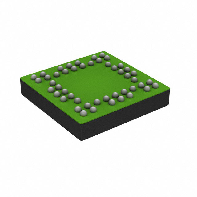
available in an 5 mm x 5 mm BGA package. The pin
out of the device is such that all the IO pins are
securely surrounded by other pins. This prevents the
secure pins from being probed during device
operation.
1
•
•
•
•
•
•
•
•
•
•
Operating supply voltage range of 2.7 V to 5.5 V
Supports EMV 4.3, ISO7816-3 and ISO7816-10
standards
Supports 1 user card and 3 secure access module
cards
IEC61000-4-2 8-kV Contact discharge esd
protection on all smartcard interface pins
Low power mode for power saving when inactive
(shutdown mode)
Automatic card deactivation in the event of short
circuit, card pull out, over temperature or power
supply fault
Integrated DC-DC boost to generate VCC for 5 V
and 3 V on all card interfaces
Automatic card clock generation for synchronous
card activation
4-byte FIFO for storing ATR from ISO7816-10
Type 1 cards
Programmable rise/fall time control for IO and
clock lines of all smartcards
Input clock frequency up to 26 MHz
Tamper proof package design
2 Applications
•
•
Device Information(1)
High-end point of sale (POS) terminals
Multi secure accesscard capable EPOS systems
PART NUMBER
PACKAGE
TCA5013
NFBGA (48)
BODY SIZE (NOM)
5.00 mm × 5.00 mm
(1) For all available packages, see the orderable addendum at
the end of the data sheet.
Simplified Schematic
VDD=VDDI= 3.3 V
CVDD = 100
µF
100 nF
CVUP =
10 µF
LVDD =
10 µH
VDDI
100 nF
DVUP
GNDP
VUP
GNDP
VDD
LX
VDDI
10k
10k
PRES
C8
C4
IOUC
CLKUC
RSTUC
VCCUC
10k 10k 10k
User
Card
Slot
200nF
GNDUC
SDA
SCL
INT
GPIO1
IOS1
CLKS1
RSTS1
VCCS1
TCA5013
GPIO2
200nF
Microcontroller
GPIO3
SAM1
Card
Slot
GNDS
GPIO4
IOS2
CLKS2
RSTS2
VCCS2
SHDN
200nF
SAM2
Card
Slot
200nF
SAM3
Card
Slot
GNDS
IOMC1
IOS3
CLKIN1
A0
TST1
TST4
TST3
TST2
GND
CLKIN2
LDOCAP
IOMC2
CLKS3
RSTS3
VCCS3
GNDS
1 µF
Copyright © 2016, Texas Instruments Incorporated
1
An IMPORTANT NOTICE at the end of this data sheet addresses availability, warranty, changes, use in safety-critical applications,
intellectual property matters and other important disclaimers. PRODUCTION DATA.
�TCA5013
SCPS253C – JANUARY 2014 – REVISED SEPTEMBER 2019
www.ti.com
Table of Contents
1
2
3
4
5
6
Features ..................................................................
Applications ...........................................................
Description .............................................................
Revision History.....................................................
Pin Configuration and Functions .........................
Specifications.........................................................
1
1
1
2
3
5
6.1
6.2
6.3
6.4
6.5
6.6
6.7
6.8
6.9
Absolute Maximum Ratings ...................................... 5
Handling Ratings....................................................... 5
Recommended Operating Conditions....................... 5
Thermal Information .................................................. 5
Electrical Characteristics—Power Supply and ESD . 6
Electrical Characteristics—Card VCC ........................ 6
Electrical Characteristics—Card RST ....................... 6
Electrical Characteristics—Card CLK ....................... 7
Electrical Characteristics—Card Interface IO, C4 and
C8............................................................................... 7
6.10 Electrical Characteristics—PRES ........................... 8
6.11 Electrical Characteristics—IOMC1 and IOMC2 ...... 9
6.12 Electrical Characteristics—CLKIN1 and CLKIN2.... 9
6.13 Electrical Characteristics—A0 and SHDN .............. 9
6.14 Electrical Characteristics—INT ............................... 9
6.15 Electrical Characteristics—GPIO ............................ 9
6.16 Electrical Characteristics—SDA and SCL............. 10
6.17 Electrical Characteristics—Fault Condition
Detection .................................................................. 10
6.18 I2C Interface Timing Requirements....................... 10
6.19 I2C Interface Timing Characteristics ..................... 10
6.20 Synchronous Type 1 Card Activation Timing
Characteristics .........................................................
6.21 Synchronous Type 2 Card Activation Timing
Characteristics .........................................................
6.22 Card Deactivation Timing Characteristics.............
6.23 Typical Characteristics ..........................................
7
8
11
11
11
Parameter Measurement Information ................ 12
Detailed Description ............................................ 13
8.1
8.2
8.3
8.4
8.5
8.6
9
11
Overview .................................................................
Functional Block Diagram .......................................
Feature Description.................................................
Device Functional Modes........................................
Programming...........................................................
Register Maps .........................................................
13
14
15
17
38
41
Application and Implementation ........................ 55
9.1 Application Information............................................ 55
9.2 Typical Application ................................................. 55
10 Power Supply Recommendations ..................... 57
10.1 Power-On-Reset ................................................... 57
11 Layout................................................................... 57
11.1 Layout Guidelines ................................................. 57
11.2 Layout Example .................................................... 58
12 Device and Documentation Support ................. 59
12.1 Trademarks ........................................................... 59
12.2 Electrostatic Discharge Caution ............................ 59
12.3 Glossary ................................................................ 59
13 Mechanical, Packaging, and Orderable
Information ........................................................... 59
4 Revision History
Changes from Revision B (January 2016) to Revision C
Page
•
Changed the Pin Configuration view ..................................................................................................................................... 3
•
Added: (Cold reset sequence) to Figure 6 ........................................................................................................................... 22
Changes from Revision A (July 2014) to Revision B
Page
•
Changed the datasheet title to "TCA5013 Feature Rich Smartcard Interface IC with 1 User Card and 3 SAM Card
Support" .................................................................................................................................................................................. 1
•
Added the Features: Tamper proof package design .............................................................................................................. 1
•
Changed the Applications ...................................................................................................................................................... 1
•
Full Version release of document ........................................................................................................................................... 1
Changes from Original (July 2014) to Revision A
•
2
Page
Full version release of document. ......................................................................................................................................... 1
Submit Documentation Feedback
Copyright © 2014–2019, Texas Instruments Incorporated
Product Folder Links: TCA5013
�TCA5013
www.ti.com
SCPS253C – JANUARY 2014 – REVISED SEPTEMBER 2019
5 Pin Configuration and Functions
ZAH Package
NFBGA 48-Pins
Bottom View
1
2
A
PRES
GPIO4
B
C8
A0
C
3
INT
4
5
6
GPIO3
GPIO2
GPIO1
SHDN
SCL
SDA
7
LDOCAP
8
9
VUP
LX
TS T4
GNDP
C4
VDD
D
CL KUC
TS T3
GND
CL KIN1
E
GNDUC
IOUC
IOMC1
GND
F
RS TUC
VCCUC
IOMC2
CL KIN2
TS T2
VDDI
G
H
RS TS3
IOS3
J
CL KS3
VCCS3
GNDS
TS T1
IOS2
GNDS
RS TS2
CL KS2
VCCS2
GNDS
IOS1
VCCS1
RS TS1
CL KS1
No t to scale
Submit Documentation Feedback
Copyright © 2014–2019, Texas Instruments Incorporated
Product Folder Links: TCA5013
3
�TCA5013
SCPS253C – JANUARY 2014 – REVISED SEPTEMBER 2019
www.ti.com
Pin Functions
PIN
NO.
4
NAME
TYPE
DESCRIPTION
User card presence detection
A1
PRES
INPUT
A2
GPIO4
I/O
General purpose IO (5-V tolerant)
A4
GPIO3
I/O
General purpose IO (5-V tolerant)
A5
GPIO2
I/O
General purpose IO (5-V tolerant)
A6
GPIO1
I/O
General purpose IO (5-V tolerant)
A8
VUP
PWR
Boost output terminal
A9
LX
PWR
Boost inductor input terminal
B1
C8
I/O
B2
A0
INPUT
B3
INT
OUTPUT
B4
SHDN
INPUT
Shutdown and reset pin
B5
SCL
INPUT
I2C clock input
B6
SDA
I/O
B7
LDOCAP
PWR
B8
TST4
NA
B9
GNDP
PWR
C2
C4
I/O
C8
VDD
PWR
D1
CLKUC
OUTPUT
D2
TST3
NA
D8
GND
PWR
D9
CLKIN1
INPUT
E1
GNDUC
PWR
E2
IOUC
I/O
User card IO pin
E8
IOMC1
I/O
User card microcontroller data IO
E9
GND
PWR
F1
RSTUC
OUTPUT
F2
VCCUC
PWR
F8
IOMC2
I/O
F9
CLKIN2
INPUT
User card external clock input pin
G2
TST2
NA
Test pin. Grounded in application.
G8
VDDI
PWR
H1
RSTS3
OUTPUT
H2
IOS3
I/O
H3
GNDS
PWR
H4
TST1
NA
Test pin. Grounded in application
H5
IOS2
I/O
IO pin for SAM2
H6
GNDS
PWR
Ground for all SAMs
H7
GNDS
PWR
Ground for all SAMs
H8
IOS1
I/O
IO pin for SAM1
H9
VCCS1
PWR
VCC for SAM1
J1
CLKS3
OUTPUT
J2
VCCS3
PWR
J4
RSTS2
OUTPUT
Reset output for SAM2
J5
CLKS2
OUTPUT
Clock output for SAM2
J6
VCCS2
PWR
J8
RSTS1
OUTPUT
Reset output for SAM1
J9
CLKS1
OUTPUT
Clock output for SAM1
User card auxiliary IO (Open Drain)
I2C address selection pin. Connect to VDDI, GND.
Interrupt output (open drain)
I2C data
Internal LDO output. Connect to 1 µf decoupling capacitor.
Test pin. Grounded in application.
Power ground
User card auxiliary IO (Open drain)
Device main power supply
User card clock
Test pin. Grounded in application.
Device ground
User card external clock input pin
User card ground pin
Device ground
User card reset output pin
User card VCC pin
SAM microcontroller data IO
Microcontroller interface supply voltage.
Reset output for SAM3
IO pin for SAM3
Ground for all SAMs
Clock output for SAM3
VCC for SAM3
VCC for SAM2
Submit Documentation Feedback
Copyright © 2014–2019, Texas Instruments Incorporated
Product Folder Links: TCA5013
�TCA5013
www.ti.com
SCPS253C – JANUARY 2014 – REVISED SEPTEMBER 2019
6 Specifications
6.1 Absolute Maximum Ratings (1) (2)
over operating free-air temperature range (unless otherwise noted) (3)
MIN
MAX
VDD
Supply voltage range
–0.3
6
V
VDDI
Interface voltage range
–0.3
4
V
Input voltage range on digital I/O pins referenced to VDDI
-0.3
VDDI +
0.3
V
Input voltage range on digital I/O pins referenced to VCC
-0.3
VCC +
0.3
V
Load current on GPIO pins
-15
mA
-6
mA
VI
IOL
(1)
(2)
(3)
Load current on INT and SDA pins
UNIT
The input negative-voltage and output voltage ratings may be exceeded if the input and output current ratings are observed.
The package thermal impedance is calculated in accordance with JESD 51-7.
Stresses beyond those listed under Absolute Maximum Ratings may cause permanent damage to the device. These are stress ratings
only, which do not imply functional operation of the device at these or any other conditions beyond those indicated under Recommended
Operating Conditions. Exposure to absolute-maximum-rated conditions for extended periods may affect device reliability.
6.2 Handling Ratings
Tstg
Storage temperature range
V(ESD)
(1)
(2)
Electrostatic discharge
Human body model (HBM), per ANSI/ESDA/JEDEC JS-001, all
pins (1)
Charged device model (CDM), per JEDEC specification
JESD22-C101, all pins (2)
MIN
MAX
UNIT
–65
150
°C
–4
4
-1.5
1.5
kV
JEDEC document JEP155 states that 500-V HBM allows safe manufacturing with a standard ESD control process.
JEDEC document JEP157 states that 250-V CDM allows safe manufacturing with a standard ESD control process.
6.3 Recommended Operating Conditions
over operating free-air temperature range (unless otherwise noted)
MIN
MAX
Supply voltage range – DC-DC enabled
2.7
5.5
V
Supply voltage Range – DC-DC disabled
5.25
5.5
V
VDDI
Interface voltage range
1.65
3.6
V
ICC(TOT)
Sum of the currents that can be drawn on all Card VCC pins
180
mA
TA
Operating temperature range
85
°C
VDD
–40
UNIT
6.4 Thermal Information
TCA5013
THERMAL METRIC (1)
ZAH
UNIT
48 PINS
RθJA
Junction-to-ambient thermal resistance
96.9
RθJC(top)
Junction-to-case (top) thermal resistance
59.0
RθJB
Junction-to-board thermal resistance
49.4
ψJT
Junction-to-top characterization parameter
1.9
ψJB
Junction-to-board characterization parameter
58.6
(1)
°C/W
For more information about traditional and new thermal metrics, see the IC Package Thermal Metrics application report, SPRA953.
Submit Documentation Feedback
Copyright © 2014–2019, Texas Instruments Incorporated
Product Folder Links: TCA5013
5
�TCA5013
SCPS253C – JANUARY 2014 – REVISED SEPTEMBER 2019
www.ti.com
6.5 Electrical Characteristics—Power Supply and ESD
VDD = VDDI = 3.3 V; LVDD = 10 µH; CVDD = 10 µF; CVUP = 10 µF; TA = –40°C to 85°C unless otherwise noted
PARAMETER
TEST CONDITIONS
VDDTH
VDD supervisor fault threshold
VDD voltage below which SUPL fault is asserted
VDDSH
VDD shutdown threshold
VDD voltage below which device will shutdown
VDDITH
VDDI shutdown threshold
VDDI voltage below which device will shutdown
IDDSH
VDD Shutdown current
Shutdown Mode at Tambient = 25 C
IDDST
VDD Standby current
Shutdown Mode at Tambient = 25°C
MIN
TYP
MAX
2.45
1.4
V
2.0
V
1.6
V
22
28
µA
300
650
µA
2
mA
IOMC1 = IOMC2 = VDDI;
CLKIN1 = CLKIN2 = GND; Tambient= 25°C
Current consumption per card interface activated
IDDA
Supply current
UNIT
2.7
VCCUC = VCCS1 = VCCS2 = VCCS3 = 5 V;
fCLKIN1 = fCLKIN2 = fCLKUC = fCLKS1 = 5 MHz;
ICCUC = ICCS1 = 55 mA; ICCS2 = ICCS3 = 2 mA;
Tambient = 25°C
235
280
mA
VDD Interface shutdown current
Shutdown Mode at 25°C
3.5
5
µA
IDDIA
VDD Interface supply current
All Card VCC = 5 V; CLKIN1 = CLKIN2 = 5 MHz; @ 25°C;
IOMC1 = IOMC2 = VDDI
290
300
µA
tWAKE
Device wakeup time
Time from
SHDN > VIH to
INT < VOL
10
ms
fOSC
Internal Oscillator Frequency
Measured on CLKUC, CLKS1,CLKS2,CLKS3
1.4
MHz
fDC-DC
DC-DC switching frequency
VDC-DC
DC-DC output voltage
VESD-IEC
IEC61000-4-2 level 4 ESD protection
on pins defined in Table 1
IDDA1 (1)
IDDISH
(1)
0.1
1
1.2
2.4
If any card VCC is 5 V
5.5
If all card VCC is 3 V or 1.8 V
3.5
MHz
V
-8
8
kV
Values highly dependent on external components like boost inductor and external rectifier. The specification is based on 75% boost
efficiency for max value and 85% efficiency for typical value
6.6 Electrical Characteristics—Card VCC
VDD = VDDI = 3.3 V; LVDD = 10 µH; CVDD = 10 µF; CVUP = 10 µF; TA = –40°C to 85°C unless otherwise noted
PARAMETER
VCC
TEST CONDITIONS
Card supply voltage
∆VCC/∆ICC
Load transient response
VRIPPLE
Peak to peak ripple voltage
ICC
Card supply Current
VDO
Current pulses I < 100 mA,
t < 400 ns
Card LDO dropout voltage
MIN
TYP
MAX
VCC = 5 V; ICC ≤ 65 mA
4.75
5
5.25
VCC = 3 V; ICC ≤ 65 mA
2.85
3
3.15
VCC = 1.8 V; ICC ≤ 45 mA
1.71
1.8
1.89
VCC = 5 V ; 40 nA.s current spike
4.65
5.35
V
VCC = 3 V ; 17.5 nA.s current spike
2.76
3.24
V
VCC = 1.8 V ; 11.1 nA.s current spike
1.62
1.98
Measured on VCC = 5 V, 3 V, 1.8 V
90
VCC = 5 V
65
VCC = 3 V
65
VCC = 1.8 V
45
ICC = 65 mA
250
UNIT
V
V
mV
mA
mV
6.7 Electrical Characteristics—Card RST
VDD = VDDI = 3.3 V; LVDD = 10 µH; CVDD = 10 µF; CVUP = 10 µF; TA = –40°C to 85°C unless otherwise noted
PARAMETER
TEST CONDITIONS
VOL - RST
Output Low voltage
IOL = -200 µA
VOH - RST
Output high voltage
IOH = 150 µA
tR - RST
Rise time
tF - RST
Fall time
6
MIN
TYP
MAX
UNIT
0.1 VCC
V
CL = 30 pF ; 10% to 90%
0.1
µs
CL = 30 pF ; 90% to 10%
0.1
µs
Submit Documentation Feedback
0.9 VCC
V
Copyright © 2014–2019, Texas Instruments Incorporated
Product Folder Links: TCA5013
�TCA5013
www.ti.com
SCPS253C – JANUARY 2014 – REVISED SEPTEMBER 2019
6.8 Electrical Characteristics—Card CLK
VDD = VDDI = 3.3 V; LVDD = 10 µH; CVDD = 10 µF; CVUP = 10 µF; TA = –40°C to 85°C unless otherwise noted
PARAMETER
TEST CONDITIONS
VOL - CLK
Output Low voltage
IOL = -100 µA
VOH - CLK
Output high voltage
IOH = 100 µA
tR - CLK/ tF - CLK
Rise/Fall time
CL = 30 pF ;
10% to 90%;
MIN
TYP
MAX
0.1 VCC
0.9 VCC
UNIT
V
V
CLK slew rate settings register =
0000b
7
CLK slew rate settings register =
0001b
9
CLK slew rate settings register =
0010b
11
CLK slew rate settings register =
0011b
13
CLK slew rate settings register =
0100b
13.5
CLK slew rate settings register =
0101b
14
CLK slew rate settings register =
0110b
15
CLK slew rate settings register =
0111b
16
CLK slew rate settings register =
1000b
17
CLK slew rate settings register =
1001b
18
CLK slew rate settings register =
1010b
19
CLK slew rate settings register =
1011b
20
CLK slew rate settings register =
1100b
21
CLK slew rate settings register =
1101b
22
CLK slew rate settings register =
1110b
23
CLK slew rate settings register =
1111b
25
ns
CLKPU-PD-SKEW
Clock pull-up / pull-down skew tR-CLK – tF-CLK / tF-CLK; CL = 30 pF
10
%
fCLK
Frequency on CLK pin
CL = 30 pF
20
MHz
D
Clock duty cycle
Internal clock = 1.2 MHz; CL = 30 pF
55
%
45
6.9 Electrical Characteristics—Card Interface IO, C4 and C8
VDD = VDDI = 3.3 V; LVDD = 10 µH; CVDD = 10 µF; CVUP = 10 µF; TA = –40°C to 85°C unless otherwise noted
PARAMETER
TEST CONDITIONS
MIN
VOL - C4, C8
Output Low Voltage
VCC = 5 V
IOL = -1 mA
VOH - C4, C8
Output Low Voltage
VCC = 5 V, 3 V, 1.8 V
IOH = 20 µA
VIL - IO, C4, C8
Output Low Voltage
VIH - IO, C4, C8
Output High Voltage
Output Low Voltage
MAX
0.5
0.9 VCC
0.6 VCC
VCC= 5 V;
IO fall time register setting = 01b
VCC= 5 V;
IO fall time register setting = 10b
VCC= 5 V;
IO fall time register setting = 11b
Product Folder Links: TCA5013
V
V
V
0.5
0.5
IOL = -1 mA
V
0.5
0.5
Submit Documentation Feedback
Copyright © 2014–2019, Texas Instruments Incorporated
UNIT
V
0.4 VCC
VCC = 5 V;
IO fall time register setting = 00b
VOL - IO, 5 V
TYP
7
�TCA5013
SCPS253C – JANUARY 2014 – REVISED SEPTEMBER 2019
www.ti.com
Electrical Characteristics—Card Interface IO, C4 and C8 (continued)
VDD = VDDI = 3.3 V; LVDD = 10 µH; CVDD = 10 µF; CVUP = 10 µF; TA = –40°C to 85°C unless otherwise noted
PARAMETER
TEST CONDITIONS
MIN
TYP
MAX
VCC= 3 V;
IO fall time register setting = 01b
VOL - IO, 3 V
Output Low Voltage
VOL - IO, 3 V, 500uA
Output Low Voltage
VCC= 3 V;
IO fall time register setting = 10b
0.3
IOL= -1 mA
0.3
VCC= 3 V;
IO fall time register setting = 11b
0.3
VCC= 3 V;
IO fall time register setting = 00b
0.3
VCC= 3 V;
IO fall time register setting = 01b
VCC= 3 V;
IO fall time register setting = 10b
Output Low Voltage
VCC= 1.8 V;
IO fall time register setting = 11b
V
0.3
0.3
IOL= -1 mA
0.18
VCC= 1.8 V;
IO fall time register setting = 01b
VOL - IO, 1.8 V, 500uA
Output Low Voltage
VCC= 1.8 V;
IO fall time register setting = 10b
V
0.3
IOL= -500
µA
VCC= 3 V;
IO fall time register setting = 11b
VOL - IO, 1.8 V
UNIT
V
0.18
IOL= -500
µA
0.18
VCC= 1.8 V;
IO fall time register setting = 11b
0.18
V
tPD - R - IOMC - IO
Rising edge
propagation delay
From IOMC pin to card IO; CL on card IO = 30 pF;
CL on IOMC = 30 pF; Prop delay measured from
70% VDDI to 70% of VCC for rising edge
400
ns
tPD - F - IOMC - IO
Falling edge
propagation delay
From IOMC pin to card IO; CL on card IO = 30 pF;
CL on IOMC = 30 pF; Prop delay measured from
30% VDDI to 30% of VCC for falling edge;
250
ns
tFO - IO
IO Line output fall time
CL = 30 pF ; 10% to 90%; IO fall time register setting
= 00b
tRO - IO
IO Line output rise time
CL = 30 pF ; 10% to 90%; IO rise time register
setting = 100b
tRO - C4, C8
C4, C8 Line output rise
time
CL = 30 pF ; 10% to 90%
1.2
µs
tFO - C4, C8
C4, C8 Line output fall
time
CL = 30 pF ; 90% to 10%
1.2
µs
tRI - IO, C4, C8
IO, C4, C8 Input rise
time
10% to 90%
1.2
µs
tFI - IO, C4, C8
IO, C4, C8 Input fall
time
90% to 10%
1.2
µs
CI - IO, C4, C8
Input capacitance
F = 1 MHz
RPU - IO, C4, C8
Pull-up resistance
IO, C4, C8 pull-up to VCC
68
ns
100
ns
4.25
10
pF
8.1
kΩ
6.10 Electrical Characteristics—PRES
VDD = VDDI = 3.3 V; LVDD = 10 µH; CVDD = 10 µF; CVUP = 10 µF; TA = –40°C to 85°C unless otherwise noted
PARAMETER
VIL - PRES
Input Low voltage
VIH - PRES
Input high voltage
ILEAK - PRES
Input leakage current
tDEB(P)
Debounce time
tDEB(D)
8
TEST CONDITION
MIN
TYP
MAX
V
1
µA
0.7 VDDI
V
Voltage on pin = VDDI
Time from transition on PRES pin to PRESL bit being
set
Time from transition on PRES pin to start of
deactivation sequence (RST going low)
Submit Documentation Feedback
UNIT
0.3 VDDI
20
ms
100
µs
Copyright © 2014–2019, Texas Instruments Incorporated
Product Folder Links: TCA5013
�TCA5013
www.ti.com
SCPS253C – JANUARY 2014 – REVISED SEPTEMBER 2019
6.11 Electrical Characteristics—IOMC1 and IOMC2
VDD = VDDI = 3.3 V; LVDD = 10 µH; CVDD = 10 µF; CVUP = 10 µF; TA = –40°C to 85°C unless otherwise noted
PARAMETER
VOL-
TEST CONDITION
Output low voltage
IOL = -100 µA
VOH - IOMC
Output high voltage
IOH = 20 µA
VIL - IOMC
Input low signal
VIH - IOMC
Input high signal
IOMC
MIN
TYP
MAX
UNIT
0.2 VDDI
V
0.8 VDDI
V
0.3 VDDI
V
0.7 VDDI
V
tPD - F - IO - IOMC
Falling edge propagation
delay
From Card IO pin to IOMC; CL on card IO = 30 pF;
Prop delay measured from 30% VCC to 30% of VDDI for
falling edge;
tPD - F - IO - IOMC
Rising edge propagation
delay
From Card IO pin to IOMC; CL on card IO = 30 pF;
Prop delay measured from 70% VCC to 70% of VDDI for
rising edge;
400
ns
tRO - IOMC
Output rise time
CL = 30 pF ; 10% to 90%
1.2
µs
tFO - IOMC
Output fall time
CL = 30 pF ; 90% to 10%
1.2
µs
tRI - IOMC
Input rise time
10% to 90%
1.2
µs
tFI - IOMC
Input fall time
90% to 10%
1.2
µs
CI - IOMC
Input capacitance
10
pF
RPU - IOMC
Pull-up resistance
Pull-up to VDDI
250
ns
11
kΩ
6.12 Electrical Characteristics—CLKIN1 and CLKIN2
VDD = VDDI = 3.3 V; LVDD = 10 µH; CVDD = 10 µF; CVUP = 10 µF; TA = –40°C to 85°C unless otherwise noted
PARAMETER
VIL - CLKIN
Input Low voltage
VIH - CLKIN
Input high voltage
tR - CLKIN
Rise time
tF - CLKIN
Fall time
fCLKIN
Input clock frequency
TEST CONDITION
MIN
TYP
MAX
UNIT
0.2 VDDI
V
10% to 90%
0.1
µs
90% to 10%
0.1
µs
26
MHz
MAX
UNIT
0.8 VDDI
V
6.13 Electrical Characteristics—A0 and SHDN
VDD = VDDI = 3.3 V; LVDD = 10 µH; CVDD = 10 µF; CVUP = 10 µF; TA = –40°C to 85°C unless otherwise noted
PARAMETER
VIL - A0, SHDN
input Low voltage
VIH - A0, SHDN
input high voltage
ILEAK - A0, SHDN
Input leakage current
CI - A0, SHDN
Input Capacitance
RPU - SHDN
Pull-up resistance on SHDN
TEST CONDITION
MIN
TYP
0.2 VDDI
V
1
µA
0.8 VDDI
V
Voltage on pin = VDDI
10
Pull-up to VDDI
pF
2.5
MΩ
6.14 Electrical Characteristics—INT
VDD = VDDI = 3.3 V; LVDD = 10 µH; CVDD = 10 µF; CVUP = 10 µF; TA = –40°C to 85°C unless otherwise noted
PARAMETER
TEST CONDITION
ILEAK - INT
Input leakage current
Voltage on pin = VDDI
VOL - INT
Output low voltage
IOL = -3 mA
MIN
TYP
MAX
UNIT
1
µA
0.2 VDDI
V
MAX
UNIT
6.15 Electrical Characteristics—GPIO
VDD = VDDI = 3.3 V; LVDD = 10 µH; CVDD = 10 µF; CVUP = 10 µF; TA = –40°C to 85°C unless otherwise noted
PARAMETER
TEST CONDITION
TYP
Output low voltage
IOL - GPIO
Output low current
ILEAK - GPIO
Input leakage current
Voltage on pin = VDDI
1
µA
State transition on GPIO to INT assertion
RPU on INT= 10 k; CL on INT 20 pF;
GPIO and INT transition referenced to 0.5 VDDI
4
µs
TPD - GPIO
IOL = -10 mA
MIN
VOL - GPIO
0.2 VDDI
10
V
mA
Submit Documentation Feedback
Copyright © 2014–2019, Texas Instruments Incorporated
Product Folder Links: TCA5013
9
�TCA5013
SCPS253C – JANUARY 2014 – REVISED SEPTEMBER 2019
www.ti.com
6.16 Electrical Characteristics—SDA and SCL
VDD = VDDI = 3.3 V; LVDD = 10 µH; CVDD = 10 µF; CVUP = 10 µF; TA = –40°C to 85°C unless otherwise noted
PARAMETER
TEST CONDITION
MIN
TYP
MAX
ILEAK - SDA, SCL
Input leakage current
Voltage on pin = VDDI
1
VOL - SDA, SCL
SDA output low voltage
IOL = -3 mA
0.1 VDDI
IOL - SDA, SCL
SDA max output low current
VOL = 0.3 V
10
VIL - SDA, SCL
Input low signal
VIH - SDA, SCL
Input high signal
0.2 VDDI
0.8 VDDI
UNIT
µA
V
mA
V
V
6.17 Electrical Characteristics—Fault Condition Detection
VDD = VDDI = 3.3 V; LVDD = 10 µH; CVDD = 10 µF; CVUP = 10 µF; TA = –40°C to 85°C unless otherwise noted
PARAMETER
TSD
Shutdown temperature
ISD
Shutdown current
ILIM
Output current limit
TEST CONDITION
MIN
TYP
125
200
MAX
UNIT
145
°C
260
mA
On card VCC pins
160
On card IO pins
–15
15
mA
On card CLK pins
–70
70
mA
On card RST pins
–20
20
mA
6.18 I2C Interface Timing Requirements (1)
STANDARD MODE
I2C BUS
PARAMETER
MIN
fscl
I2C clock frequency
tsch
I2C clock high time
tscl
I2C clock low time
MAX
I C spike time
tsds
I2C serial data setup time
tsdh
I2C serial data hold time
MIN
100
FAST MODE PLUS
(FM+) I2C BUS
MAX
MIN
400
UNIT
MAX
1000
kHz
4
0.6
0.26
μs
4.7
1.3
0.5
μs
2
tsp
FAST MODE
I2C BUS
50
50
50
ns
250
100
50
ns
0
0
0
ns
2
ticr
I C input rise time
1000
300
120
ns
ticf
I2C input fall time
300
300
120
ns
tocf
I2C output fall time; 10 pF to 400 pF bus
300
300
120
μs
2
tbuf
I C bus free time between Stop and Start
4.7
1.3
0.5
μs
tsts
I2C Start or repeater start condition setup time
4.7
0.6
0.26
μs
tsth
I2C Start or repeater start condition hold time
4
0.6
0.26
μs
tsps
I2C Stop condition setup time
4
0.6
0.26
μs
(1)
Refer to the Parameter Measurement Information section for more information.
6.19 I2C Interface Timing Characteristics (1)
MAX
UNIT
tvd(data)
Valid data time; SCL low to SDA output valid
PARAMETER
450
ns
tvd(ack)
Valid data time of ACK condition; ACK signal from SCL low to SDA (out) low
450
ns
(1)
10
MIN
TYP
Refer to Parameter Measurement Information section for more information.
Submit Documentation Feedback
Copyright © 2014–2019, Texas Instruments Incorporated
Product Folder Links: TCA5013
�TCA5013
www.ti.com
SCPS253C – JANUARY 2014 – REVISED SEPTEMBER 2019
6.20 Synchronous Type 1 Card Activation Timing Characteristics
PARAMETER
TEST CONDITION
MIN
TYP MAX
UNIT
tS1-RST-HI
CL= 30 pF ; VCC= 5 V; See Figure 4.
60
70
80
µs
tS1-CLK-HI
CL= 30 pF ; VCC= 5 V; See Figure 4.
10
12.5
15
µs
tS1-RST-CLK
CL= 30 pF ; VCC= 5 V; See Figure 4.
25
28
32
µs
tS1-CLK-RST
CL= 30 pF ; VCC= 5 V; See Figure 4.
25
28
32
µs
tS1-CLK-LO
CL= 30 pF ; VCC= 5 V; See Figure 4.
70
80
90
µs
tS1-CLK-PER
CL= 30 pF ; VCC= 5 V; See Figure 4.
22.5
25
27.5
µs
tS1-ATR-SETUP
CL= 30 pF ; VCC= 5 V; See Figure 4.
1
Duty cycle
CL= 30 pF ; VCC= 5 V; See Figure 4.
45
50
55
µs
%
6.21 Synchronous Type 2 Card Activation Timing Characteristics
PARAMETER
TEST CONDITION
MIN
TYP MAX
UNIT
tS2-VCC-CLK
CL= 30 pF ; VCC= 5 V; See Figure 5.
5
20
tS2-CLK-C4
CL= 30 pF ; VCC= 5 V; See Figure 5.
14
18
22
µs
µs
tS2-CLK-HI
CL= 30 pF ; VCC= 5 V; See Figure 5.
7
9
11
µs
6.22 Card Deactivation Timing Characteristics
PARAMETER
TEST CONDITION
tDEAC-TOTS
CL= 30 pF ; VCC= 5 V; See Figure 7.
tDEAC-RST-CLK
CL= 30 pF ; VCC= 5 V; See Figure 7.
tDEAC-RST-IO
CL= 30 pF ; VCC= 5 V; See Figure 7.
tDEAC-RST-VCC
CL= 30 pF ; VCC= 5 V; See Figure 7.
MIN
TYP
MAX
0.5
0.6
ms
10
12
15
µs
22
24
26
µs
45
UNIT
µs
6.23 Typical Characteristics
CLK Rise / Fall Time (ns)
30
CLK Rise Time
CLK Fall Time
25
20
15
10
1111
1110
1101
1100
1011
1010
1001
1000
0111
0110
0101
0100
0011
0010
0001
0
0000
5
Clock Slew Rate Settings Register Value (ns)
C001
CL = 30 pF
Figure 1. CLK Rise/Fall Time vs Clock Slew Rate Settings Register Value
Submit Documentation Feedback
Copyright © 2014–2019, Texas Instruments Incorporated
Product Folder Links: TCA5013
11
�TCA5013
SCPS253C – JANUARY 2014 – REVISED SEPTEMBER 2019
www.ti.com
7 Parameter Measurement Information
tf
SDA
tr
tSU;DAT
70 %
30 %
70 %
30 %
cont.
tHD;DAT
tf
tVD;DAT
tHIGH
tr
70 %
30 %
SCL
70 %
30 %
70 %
30 %
tHD;STA
70 %
30 %
cont.
tLOW
9th clock
1 / fSCL
S
1st clock cycle
tBUF
SDA
tSU;STA
tHD;STA
tVD;ACK
tSP
tSU;STO
70 %
30 %
SCL
Sr
P
9th clock
S
002aac938
VIL = 0.3 VDDI
VIH = 0.7 VDDI
Figure 2. Parameter Measurement Information for I2C Timing Characteristics and Requirements
12
Submit Documentation Feedback
Copyright © 2014–2019, Texas Instruments Incorporated
Product Folder Links: TCA5013
�TCA5013
www.ti.com
SCPS253C – JANUARY 2014 – REVISED SEPTEMBER 2019
8 Detailed Description
8.1 Overview
TCA5013 is a smartcard interface IC that enables POS terminals to interface with EMV4.3 and ISO7816-3 and
ISO7816-10 compliant smartcards. The device has 4 smartcard interfaces (1 user card and 3 SAM cards).
TCA5013 is capable of card activation and deactivation per EMV4.3, ISO7816-3 and ISO7816-10 standards.
TCA5013 has two power supply pins - VDD and VDDI. VDD is the main power supply for the device and VDDI is
the reference supply for the interface operating voltage. VDD and VDDI need to ramped to within the
recommended operating conditions for the device to operate properly. Upon power up an internal Power-OnReset circuit initializes the digital core with all the registers in their default state as described in Register Maps.
TCA5013 can operate in various functional modes as defined in Device Functional Modes. When one of the
device power supplies is not applied, that is, VDD < VDDSH or VDDI < VDDITH the device is in Power Off Mode. None
of the device functions are available in this mode. Shutdown Mode is the lowest power operating mode in the
device. Shutdown mode is entered by asserting the SHDN = 0 when VDD > VDDSH and VDDI > VDDITH. The device
can detect card insertion and removal even in Shutdown mode. The device is in Standby mode when VDD >
VDDSH or VDDI > VDDITH and the SHDN pin = 1. When any of the 4 smartcard interfaces is activated, the device
enters active mode (see Active Mode). The user card interface module can be activated in synchronous type 1,
synchronous type 2, asynchronous or manual operation mode. For synchronous type 1 and synchronous type 2
operation modes, the device can automatically generate activation sequences per the ISO7816-10 standard (see
Synchronous Type 1 Operating Mode and Synchronous Type 2 Operating Mode). For asynchronous cards the
device performs the activation sequence and also verifies the response from the card meets the requirements
per ISO7816-3 and EMV4.3 standards (see Asynchronous Operating Mode). The device also supports WARM
reset ( see Warm Reset Sequence) and card deactivation (see Deactivation Sequence) of smartcards per the
ISO7816-3 and EMV4.3 standards. The SAM card interface modules can only be activated in aynchronous
operation mode.
All smartcard interfaces have the standard CLK, IO and RST pins (as defined by EMV4.3 and ISO7816
standards). All these pins are designed to have internal current limiting to prevent device damage when shorted.
CLK and IO pins also provide automatic level translation to the voltage at which the card has been activated.
Rrise time and fall time of the CLK and IO pins can also be controlled using digital register settings (see IO Rise
Time and Fall Time control and CLK Rise Time and Fall Time Control). In addition to the CLK, IO and RST pins
the user card interface also has PRES pin to detect card insertion and removal (see User Card Insertion /
Removal Detection). C4 and C8 pins, as defined by ISO7816-10, are also present on the user card interface (see
User Card Interface Module).
The device has internal boost and LDOs to generate the card activation voltage depending on the operating
voltage required by the specific card being interfaced with. It also has a voltage supervisor that monitors VDD and
VDDI and responds as described in Interrupt Operation . The power management section is described in more
detail in Power Management.
In addition to these functions the device provides 8kV IEC 61000-4-2 ESD protection on all pins that interface to
smartcards. This removes the need for any external ESD protection on the board, thereby providing system
robustness without compromising system security (removable components on secure lines).
TCA5013 is configured using a standard I2C interface that is capable of up to 1 MHz operation. The I2C interface
is also used to read the status of various fault conditions that the device can detect. The I2C operation is
described in detail in I2C Interface Operation.
Submit Documentation Feedback
Copyright © 2014–2019, Texas Instruments Incorporated
Product Folder Links: TCA5013
13
�TCA5013
SCPS253C – JANUARY 2014 – REVISED SEPTEMBER 2019
www.ti.com
8.2 Functional Block Diagram
VDD
LX
VUP
User Card Interface
Module
LDOCAP
LDO
Boost
GNDP
GNDP
User card IO
IOMC1
multiplexer
CLKIN1
User card
clock divider
and multiplexer
Card V CC LDO
VCCUC
IO level translator
IOUC
CLK level translator
CLKUC
RST level translator
RSTUC
C4 & C8 buffers
C4
C8
PRES detection logic
PRES
GNDUC
VDDI
Voltage
Oscillator
supervisor
SAM 1 Interface Module
IOMC2
Card V CC LDO
VCCS1
IO level translator
IOS1
CLK level translator
CLKS1
RST level translator
RSTS1
GNDS
SAM card
IO multiplexer
CLKIN2
SAM clock
SAM 2 Interface Module
divider and
multiplexer
Card V CC LDO
VCCS2
SCL
2
I C
SDA
interface
IO level translator
IOS2
CLK level translator
CLKS2
RST level translator
RSTS2
GNDS
Digital core
SAM 3 Interface Module
and register map
INT
SHDN
A0
GNDP
GPIO1
GPIO2
TST1
14
TST2
GPIO3
Card V CC LDO
VCCS3
IO level translator
IOS3
CLK level translator
CLKS3
RST level translator
RSTS3
GNDS
GPIO4
TST3
TST4
Submit Documentation Feedback
Copyright © 2014–2019, Texas Instruments Incorporated
Product Folder Links: TCA5013
�TCA5013
www.ti.com
SCPS253C – JANUARY 2014 – REVISED SEPTEMBER 2019
8.3 Feature Description
8.3.1 Card Interface Modules
TCA5013 has 1 user card interface module and 3 SAM card interface modules. All card modules have level
translators and an LDO to support interfacing with smartcards operating at different voltages.
8.3.2 SAM Card Interface Modules
All SAM card interface modules can operate per the EMV4.3 and ISO7816-3 standard and support asynchronous
operating mode. All SAM card interface modules have the standard IO, CLK and RST pins. Detailed operation of
these pins is described in section IO operation, CLK operation and RST operation.
8.3.3 User Card Interface Module
User card interface module can also operate per the EMV4.3 and ISO7816-3 standard and support
asynchronous operating mode. In addition, the user card interface module also supports synchronous type 1
operating mode and synchronous type 2 operating mode, per ISO7816-10. Like the SAM card interface modules,
the user card interface module also has IO, CLK, and RST pins. The user card interface module also has a
PRES pin that is used for detection of user card insertion or removal.
C4 and C8 are two pins that are only present on the user card interface. These are open drain bi-directional IOs
that are controlled by the bit [5] and bit [4] of user card synchronous mode settings register (Reg 0x09) when the
card interface is activated. These bits act as both control and status bits for the C4 and C8 signals. If a ‘0’ is
written to either of these bits the corresponding pin is driven low by the TCA5013. However, when a ‘1’ is written
to the register bit, the corresponding pin is pulled up by an internal pull-up resistor. In this state an external
device can drive the pin low. If the pin is driven low, then the corresponding bit in the register changes to reflect
the status of the pin.
8.3.4 Clock Division and Multiplexing
TCA5013 card interface modules all have a CLK pin that provide a clock signal that is used for smartcard
operation. This clock signal is generated based on an internal oscillator or from the CLKIN1/CLKIN2 input clock
signals, by the clock divider and multiplexer circuitry. The user card has a dedicated clock divider and
multiplexer. The user card CLK output can be a configured to be a function of the CLKIN1 frequency or the
internal oscillator frequency. CLKIN2 is shared by all the SAM card interface modules. The CLK output of each
SAM card can be independently configured based on the CLKIN2 frequency or the internal oscillator frequency.
CLK operation section describes the clock division and multiplexing in detail.
8.3.5 IO Multiplexing
IOMC1 and IOMC2 are connected to the IO pins in the card interface modules through IO multiplexer blocks.
The user card IO module has a dedicated IO multiplexer, that can be connect or disconnect IOUC from the
IOMC1 pin. The IOMC2 is connected to the SAM card interface modules IO pins through the SAM IO multiplexer
block. The IOMC2 can only be connected to one of the SAM interface modules at any given time. IO operation
section describes IO multiplexing in detail.
8.3.6 GPIO Operation
The TCA5013 has four 5 V tolerant open drain GPIO pins that can be configured as inputs or outputs through
device settings register (Reg 0x42). If configured as outputs, each is capable of sinking up to 10mA of current. If
configured as inputs they will assert the INT line when a state change occurs on the pin. The minimum pulse
width for transition detection is 10 µs, that is, when a state transition occurs on a GPIO configured as an input, it
needs to hold its state for a minimum of 10 µs in order to guarantee detection by the TCA5013. This, however,
does not imply any glitch rejection on the GPIO pins. The GPIOs are available in Standby Mode and Active
Mode. GPIO state transitions are not tracked in shutdown mode.
8.3.7 Power Management Features
TCA5013 has a DC-DC boost and card LDOs that enable it to generate regulated smart card VCC from its input
power rails (VDD and VDDI). It also has an internal LDO that is used to power its internal circuits. The TCA5013
devices also have a voltage supervisor that monitors the VDD and VDDI rails to ensure they are stable and usable
for smartcard operation.
Submit Documentation Feedback
Copyright © 2014–2019, Texas Instruments Incorporated
Product Folder Links: TCA5013
15
�TCA5013
SCPS253C – JANUARY 2014 – REVISED SEPTEMBER 2019
www.ti.com
Feature Description (continued)
8.3.8 ESD Protection
All the smart card interface pins in the TCA5013 devices are designed with in built IEC61000-4-2 level 4 8kV
contact ESD protection. Table 1 shows a list of pins with the 8kV ESD protection. The pins not listed below all
have 4kV HBM ESD protection.
Table 1. List of Pins with 8kV IEC ESD Protection
PIN
SYMBOL
TYPE
DESCRIPTION
A1
PRES
INPUT
User card presence detection
B1
C8
IO
User card auxiliary IO (Open Drain)
C2
C4
IO
User card auxiliary IO (Open Drain)
D1
CLKUC
OUTPUT
User card clock
E2
IOUC
IO
User card IO
F1
RSTUC
OUTPUT
User card RST
F2
VCCUC
PWR
User card VCC
H1
VCCUC
OUTPUT
SAM3 RST
H2
IOS3
IO
SAM3 IO
H5
IOS2
IO
SAM2 IO
H8
IOS1
IO
SAM1 IO
H9
VCCS1
PWR
SAM1 VCC
J1
CLKS3
OUTPUT
SAM3 CLK
J2
VCCS3
PWR
SAM3 VCC
J4
RSTS2
OUTPUT
SAM2 RST
J5
CLKS2
OUTPUT
SAM2 CLK
J6
VCCS2
PWR
SAM2 VCC
J8
RSTS1
OUTPUT
SAM1 RST
J9
CLKS1
OUTPUT
SAM1 CLK
8.3.9 I2C interface
The device has a standard I2C interface that is used to configure the device and to read the status of the device.
For detailed I2C operation refer to I2C Interface Operation.
16
Submit Documentation Feedback
Copyright © 2014–2019, Texas Instruments Incorporated
Product Folder Links: TCA5013
�TCA5013
www.ti.com
SCPS253C – JANUARY 2014 – REVISED SEPTEMBER 2019
8.4 Device Functional Modes
At any given time the TCA5013 can be in one of several different functional modes. Figure 3 diagram shows the
different functional modes and describes how the device transitions from one mode to another. The blue bubbles
represent actual functional modes and the white bubbles represent transitional states that are used to move from
one functional mode to another.
Power off mode
VDD > VDDSH
VDDI > VDDITH
SHDN = 0
VDD > VDDSH
VDDI > VDDITH
SHDN = 1
VDD < VDDSH
or
VDDI < VDDITH
State change
on PRES pin
Shutdown mode
Assert INT
VDD < VDDSH
or
VDDI < VDDITH
SHDN = 1
Deactivate all
card slots
Power on
Reset
SHDN = 0
Standby mode
Deactivate all
card slots
VCC fail
Deactivate all
card slots
SHDN = 0
Card
activation
command
VCC Check
VDD < VDDTH
Or over
temperature
VCC
active
No other
card slot
active
VDDI < VDDITH
Active mode
Other cards
still active
Over current card
removal or
deactivation
command
Deactivate all
card slots
Figure 3. Device Operating Modes
Submit Documentation Feedback
Copyright © 2014–2019, Texas Instruments Incorporated
Product Folder Links: TCA5013
17
�TCA5013
SCPS253C – JANUARY 2014 – REVISED SEPTEMBER 2019
www.ti.com
Device Functional Modes (continued)
8.4.1 Power Off Mode
The TCA5013 is in power off mode when VDD < VDDSH or VDDI < VDDITH. In power off mode none of the device
features are functional and available for use.
8.4.2 Shutdown Mode
TCA5013 is in shutdown mode when all the below conditions are true.
• VDD > VDDSH
• VDDI > VDDITH
• SHDN = 0
Shutdown mode is a low power mode where all circuits except card insertion detection circuitry are shutdown.
Even I2C communication is disabled in shutdown mode. The only active circuit in the device is card insertion
detection circuit on the PRES pin (see User Card Insertion / Removal Detection). Shutdown mode is entered
from Active Mode or Standby Mode by asserting the SHDN pin. When entering shutdown mode from Active
Mode all active card interfaces are automatically deactivated.
8.4.3 Standby Mode
The TCA5013 is in standby mode when all the below conditions are true.
• VDD > VDDSH
• VDDI > VDDITH
• SHDN = 1
• No card interfaces are activated.
In standby mode, the device I2C and card detection circuits are fully functional. All other circuits are ready to be
activated based on I2C commands received from the microcontroller. Standby mode is entered from shutdown
mode by releasing the SHDN pin or from power down mode by powering up the device or from active mode by
deactivating all card interfaces.
8.4.4 Active Mode
The TCA5013 is in active mode when all the below conditions are true.
• VDD > VDDSH
• VDDI > VDDITH
• SHDN = 1
• At least one card interface is activated
In active mode, the device is fully functional with at least one of the card interfaces activated. The DC-DC
Boost and card LDOs are active and provide power to the card VCC pins of the active card interfaces. Active
mode can only be entered from standby mode by activating one of the card interfaces. When the device is in
active mode, the individual card interfaces can be active in different operating modes. The user card supports
Asynchronous Operating Mode, Synchronous Type 1 Operating Mode,Synchronous Type 2 Operating Mode,
or Manual Operating Mode. The SAM card interfaces can only be activated in asynchronous activation mode.
18
Submit Documentation Feedback
Copyright © 2014–2019, Texas Instruments Incorporated
Product Folder Links: TCA5013
�TCA5013
www.ti.com
SCPS253C – JANUARY 2014 – REVISED SEPTEMBER 2019
Device Functional Modes (continued)
8.4.4.1 User Card Operating Mode Selection
The user card interface in the TCA5013 can be activated in different operating modes. When the
START_ASYNC bit (bit [0]; Reg 0x01) is set the user card interface is activated in asynchronous operating mode.
When START_SYNC bit (bit[0]; Reg 0x09) is set the user card interface is activated in synchronous type1,
synchronous type 2 or manual operating mode. When the START_SYNC bit is set, the operating mode is
determined by the ACTIVATION_TYPE bit (bit [6]; Reg 0x09) and CARD_TYPE bit (bit [7] Reg 0x09).
If ACTIVATION_TYPE bit (bit [6]; Reg 0x09) is set to ‘0’, the user card interface is activated in manual operating
mode. If the ACTIVATION_TYPE bit is set to’1’, the user card interface is set for automatic activation, where it
will be activated in synchronous type 1 or synchronous type 2 operating mode based on CARD_TYPE bit (bit [7]
Reg 0x09). If CARD_TYPE bit is set to ‘1’, the card interface is activated in synchronous type 2 operating mode.
If CARD_TYPE bit is set to ‘0’ the card interface is activated in synchronous type 1 operating mode.
Any changes made to the START_SYNC, START_ASYNC, CARD_TYPE or ACTIVATION_TYPE bits when the
user card interface is active, will be ignored and will have no effect on the device. These new settings will take
effect only on the next card interface activation following deactivation (see Deactivation Sequence).
8.4.4.2 Synchronous Type 1 Operating Mode
Synchronous type 1 operating mode is only supported on the user card interface. To enter synchronous
operating mode, the user card interface goes through the synchronous type 1 activation sequence. Figure 4
shows the synchronous type 1 activation sequence.
CLKIN1 shall be low before the synchronous type 1 activation sequence is initiated. The following bit settings are
required to initiate a synchronous type 1 activation sequence.
• ACTIVATION_TYPE (bit [6]; Reg 0x09) = 1
• CARD_TYPE (bit [7]; Reg 0x09) = 0
• START_SYNC (bit [0]; Reg 0x09) = 1
VCCUC
t
S1-RST-HI
All High levels refer to 0 .9 Vcc
All Low levels refer to 0 . 1 Vcc
t
RSTUC
t
S1-RST-CLK
t
t R = t F < 0. 5 μs
S1-CLK-RST
S1-CLK-HI
t
S1-CLK-LO
t
S1-CLK-PER
32 Clock cycles (4 Bytes)
CLKUC
t
t
S1-ATR-SETUP
Bit 0
IOUC
S1-ATR-SETUP
Bit 1 to Bit 30 of
ATR response
Bit 31
C4
C8
INT
Figure 4. Synchronous Type 1 Activation Sequence
Submit Documentation Feedback
Copyright © 2014–2019, Texas Instruments Incorporated
Product Folder Links: TCA5013
19
�TCA5013
SCPS253C – JANUARY 2014 – REVISED SEPTEMBER 2019
www.ti.com
Device Functional Modes (continued)
Once synchronous type 1 activation has been initiated, the following sequence of events occurs on the user card
interface:
• VCCUC, RSTUC, CLKUC, C4, C8 and IOUC are all default low.
• VCC is applied to the VCCUC pin per the SET_VCC_UC bit (bit[7:6]; Reg 0x01).
• After VCC is stable RSTUC and CLKUC pulses are applied per tS1-RST-HI and tS1-CLK-HI defined in Table 2.
• After VCC is stable, the IOUC line is pulled up to VCC .
• After VCC is stable C4 and C8 reflect the value in their corresponding I2C register bits (bit[5] and bit[4]; Reg
0x09).
• RSTUC is held low while the CLKUC line starts oscillating with a frequency of ~40Khz (generated from
internal oscillator).
• The IO line is sampled on the 32 rising or falling (based on bit[1]; Reg 0x09) edges of CLK and stored in the
FIFO registers 0AH to 0DH.
• At the end of the 32nd CLK pulse, the CLKUC is held low and the CLKUC pin is controlled by the clock
settings register (Reg 0x02).
• IOUC is connected to IOMC1 if IO_EN_UC bit (bit[5] Reg 0x01) is set to 1.
• INT_SYNC_COMPLETE bit (Bit[1]; REG 0x41) is set and the INT line is asserted low.
• IOMC1 shall stay pulled up to VDDI i.e. IOMC1 shall not be pulled low until INT is asserted.
• CLKIN1 shall toggle only after INT is asserted.
• RSTUC is controllable by I2C after INT is asserted.
Table 2. Synchronous Type 1 Card Activation Timing Characteristics
MIN
TYP
MAX
UNIT
tS1-RST-HI
60
70
80
µs
tS1-CLK-HI
10
12.5
15
µs
tS1-RST-CLK
25
28
32
µs
tS1-CLK-RST
25
28
32
µs
tS1-CLK-LO
70
80
90
µs
tS1-CLK-PER
22.5
25
27.5
µs
Duty cycle
45
50
55
%
8.4.4.3 Synchronous Type 2 Operating Mode
Synchronous type 2 operating mode is only supported on the user card interface. To enter synchronous
operating mode, the user card interface goes through the synchronous type 2 activation sequence. Figure 5
shows the synchronous type 2 activation sequence.
CLKIN1 shall be low before the synchronous type 2 activation sequence is initiated. The following bit settings are
required to initiate a synchronous type 1 activation sequence.
• ACTIVATION_TYPE (bit [6]; Reg 0x09) = 1
• CARD_TYPE (bit [7]; Reg 0x09) = 1
• START_SYNC (bit [0]; Reg 0x09) = 1
20
Submit Documentation Feedback
Copyright © 2014–2019, Texas Instruments Incorporated
Product Folder Links: TCA5013
�TCA5013
www.ti.com
VCCUC
SCPS253C – JANUARY 2014 – REVISED SEPTEMBER 2019
t S2-VCC-CLK
t
S2-CLK-C4
All High levels refer to 0 .9 Vcc
All Low levels refer to 0 . 1 Vcc
t R = t F < 0 .5 μs
CLKUC
t S2-CLK-HI
C4
IOUC
INT
RST stays LOW through entire activation
RSTUC
Figure 5. Synchronous Type 2 Activation Sequence
Once synchronous type 2 activation has been initiated, the following sequence of events occur on the user card
interface:
• VCCUC, RSTUC, CLKUC, C4, C8 and IOUC are all default low.
• VCC is applied to the VCCUC pin per the SET_VCC_UC bit (bit[7:6]; Reg 0x01).
• A single pulse is applied to CLKUC per the tS2-CLK-HI timing defined in Table 3.
• The C4 line is held low through the VCC ramp.
• The C4 line is released high per the tS2-CLK-C4 timing defined in Table 3.
• After C4 is released CLKUC is controlled by clock settings register (Reg 0x02).
• After VCC is stable, the IOUC line is pulled up to VCC.
• After VCC is stable, C8 reflects value in bit [4] Reg 0x09.
• IOUC is connected to IOMC1 if IO_EN_UC bit (bit[5] Reg 0x01) is set to 1.
• INT_SYNC_COMPLETE bit (Bit[1]; REG 0x41) is set and the INT line is asserted low.
• IOMC1 shall stay pulled up to VDDI , that is, IOMC1 shall not be pulled low until INT is asserted.
• CLKIN1 shall toggle only after INT is asserted.
• RSTUC is controllable by I2C after INT is asserted.
Table 3. Synchronous Type 2 Card Activation Timing Characteristics
MIN
TYP
tS2-VCC-CLK
5
20
MAX
UNIT
tS2-CLK-C4
14
18
22
µs
tS2-CLK-HI
7
9
11
µs
µs
Submit Documentation Feedback
Copyright © 2014–2019, Texas Instruments Incorporated
Product Folder Links: TCA5013
21
�TCA5013
SCPS253C – JANUARY 2014 – REVISED SEPTEMBER 2019
www.ti.com
8.4.4.4 Manual Operating Mode
Manual operating mode is only supported on the user card interface. Unlike the other operating modes, the
manual operating mode does not have a defined activation sequence. CLKIN1 shall be low before the manual
activation sequence is initiated. The following bit settings are required to initiate a synchronous type 1 activation
sequence.
• ACTIVATION_TYPE (bit [6]; Reg 0x09) = 0
• START_SYNC (bit [0]; Reg 0x09) = 1
Once manual activation has been initiated the following sequence of events occur on the user card interface.
• VCCUC, RSTUC, CLKUC, C4, C8 and IOUC are all default low.
• VCC is applied to the VCCUC pin per the SET_VCC_UC bit (bit[7:6]; Reg 0x01)
• After VCC is stable, the IOUC line is pulled up to VCC
• After VCC is stable C4 and C8 reflect the value in their corresponding I2C register bits (bit[5] and bit[4]; Reg
0x09)
• IOUC is connected to IOMC1 if IO_EN_UC bit (bit[5] Reg 0x01) is set to 1.
• INT_SYNC_COMPLETE bit (Bit[1]; REG 0x41) is set and the INT line is asserted low.
• IOMC1 shall stay pulled up to VDDI i.e. IOMC1 shall not be pulled low until INT is asserted.
• CLKIN1 shall toggle only after INT is asserted.
• RSTUC is controllable by I2C after INT is asserted.
8.4.4.5 Asynchronous Operating Mode
Asynchronous operating mode is supported on all card interfaces. To enter asynchronous operating mode, the
user card interface goes through the asynchronous activation sequence. Figure 6 shows the asynchronous
activation sequence. CLKIN1 shall be toggling before the asynchronous activation sequence is initiated. The
asynchronous activation sequence is initiated by setting the START_ASYNC bit (bit[0]) of the card interface
settings register (Reg 0x01 for User card, Reg 0x11 for SAM1, Reg 0x21 for SAM1, Reg 0x31 for SAM3) to ‘1’.
VCC
IO
200 CLK
cycles
IO ignored
200 CLK cycles
IO ignored
42100 CLK
Cycles
(EARLY+MUTE)
42100 CLK
Cycles
(EARLY+MUTE)
CLK
EARLY
answer
check
ATR Valid
Window
MUTE
answer
check
EARLY
answer
check
ATR Reception
Window
MUTE
answer
check
RST
Card activation sequence
(Cold reset sequence)
Warm reset sequence
Figure 6. Asynchronous Activation and Warm Reset Sequence
22
Submit Documentation Feedback
Copyright © 2014–2019, Texas Instruments Incorporated
Product Folder Links: TCA5013
�TCA5013
www.ti.com
SCPS253C – JANUARY 2014 – REVISED SEPTEMBER 2019
Once asynchronous activation has been initiated, the following sequence of events takes place on the card
interface:
• VCC, RST, CLK, C4, C8 and IO are all default low.
• VCC is applied to the VCC pin per the SET_VCC bits (bit [7:6] of card interface settings register).
• After VCC is stable, the IO line is pulled up to VCC.
• After VCC is stable C4 and C8 reflect the value in their corresponding I2C register bits (bit[5] and bit[4]; Reg
0x09).
• IO is connected to IOMC if IO_EN bit (bit[5] of card interface settings register) is set to 1.
• The CLK line starts to oscillate based on the card clock settings register. Any change on the IO line during
the first 200 card clock cycles on the CLK pin is ignored.
• After the first 42100 CLK cycles, the RST line is driven high.
• If there is a high to low transition on the IO line before RST is high, the EARLY bit (bit[6]) and MUTE bit
(bit[5]) of the card interface status register (Reg 0x00 for user card, Reg 0x10 for SAM1, Reg 0x20 for SAM2
and Reg 0x30 for SAM3) is set and the INT pin is asserted low.
• After RST is high, an internal counter starts counting CLK cycles. If there is a high to low transition on IO pin
before the internal counter reaches the value defined by in the EARLY_COUNT_HI register (Reg 0x03 for
user card, Reg 0x13 for SAM1, Reg 0x23 for SAM2, Reg 0x33 for SAM3) and EARLY_ COUNT_LO Register
(Reg 0x04 for user card, Reg 0x14 for SAM1, Reg 0x24 for SAM2, Reg 0x34 for SAM3) then the EARLY bit
in the card interface status register is set and INT is asserted.
• If the internal counter reaches the value defined by MUTE_COUNT_HI register (Reg 0x05 for user card, Reg
0x15 for SAM1, Reg 0x25 for SAM2, Reg 0x35 for SAM3) and MUTE_COUNT_LO (Reg 0x06 for user card,
Reg 0x16 for SAM1, Reg 0x26 for SAM2, Reg 0x36 for SAM3) registers without a high to low transition on
the IO line, then the MUTE bit in the card interface status registers is set and INT pin is asserted low.
If the first high to low transition on IO pin happens very close to the clock edges (within ~10 ns) that defines the
ATR VALID window (see Figure 6), the TCA5013 response would be non-deterministic, that is, it may not be able
to identify whether the transition happened before or after the edge. This implies that the MUTE bit may or may
not be set if the IO transition happens very close to the clock edge defining the end of the ATR VALID window.
Likewise, if the IO transition happens very close to the clock edge defining the beginning of the EARLY window,
it may or may not set the EARLY bit.
8.4.4.6 Warm Reset Sequence
When a card interface is active in asynchronous mode, it is possible to initiate a warm reset sequence on the
card interface. The warm reset sequence is initiated by setting the WARM bit (bit [3]) of the card interface
settings register to ‘1’. Once warm reset is initiated the below sequence of events takes place on the card
interface.
• VCC is already ramped and stable per the SET_VCC bits (bit[7:6] of card interface settings register).
• CLK continues to oscillate per the card clock settings register.
• RST pin is pulled low (high before warm reset was initiated).
• C4 and C8 continue to reflect the value in their corresponding I2C register bits (bit[5] and bit[4]; Reg 0x09).
• IO stays connected to IOMC if IO_EN bit (bit5 of card interface settings register) is set to 1.
• Any change on the IO line during the first 200 card clock cycles after RST goes low is ignored.
• After the first 42100 CLK cycles, the RST line is driven high.
• If there is a high tow low transition on the IO line before RST is high, the EARLY bit (bit6) and MUTE bit (bit5)
of the card interface status register (Reg 0x00 for user card, Reg 0x10 for SAM1, Reg 0x20 for SAM2 and
Reg 0x30 for SAM3) is set and the INT pin is asserted low.
• After RST is high, an internal counter starts counting CLK cycles. If there is a high to low transition on IO pin
before the internal counter reaches the value defined by in the EARLY_COUNT_HI register (Reg 0x03 for
user card, Reg 0x13 for SAM1, Reg 0x23 for SAM2, Reg 0x33 for SAM3) and EARLY_ COUNT_LO Register
(Reg 0x04 for user card, Reg 0x14 for SAM1, Reg 0x24 for SAM2, Reg 0x34 for SAM3) then the EARLY bit
in the card interface status register is set and INT is asserted.
• If the internal counter reaches the value defined by MUTE_COUNT_HI register (Reg 0x05 for user card, Reg
0x15 for SAM1, Reg 0x25 for SAM2, Reg 0x35 for SAM3) and MUTE_COUNT_LO (Reg 0x06 for user card,
Reg 0x16 for SAM1, Reg 0x26 for SAM2, Reg 0x36 for SAM3) registers without a high to low transition on
the IO line, then the MUTE bit in the card interface status registers is set and INT pin is asserted low.
Submit Documentation Feedback
Copyright © 2014–2019, Texas Instruments Incorporated
Product Folder Links: TCA5013
23
�TCA5013
SCPS253C – JANUARY 2014 – REVISED SEPTEMBER 2019
www.ti.com
8.4.4.7 Deactivation Sequence
After a card interface has been activated in a certain operating mode, it can be deactivated by I2C command or
certain interrupt events (see Interrupt Operation). The deactivation sequence is the same regardless of what
operating mode the card interface is in.
Figure 7 shows the deactivation sequence initiated by card extraction on the user card interface. It is to be noted
that the deactivation sequence starts 100 µs after the transition on PRES. This delay is intended to provide a
debounce period that provides unintended deactivation due to any glitch on the PRES pin. As mentioned
previously any of the card interfaces may be deactivated due to a supervisor fault, over current fault or over
temperature fault. In these cases there is no debounce period and the deactivation sequence is initiated as soon
as the internal fault signal is asserted.
Figure 8 shows the deactivation of any card interface initiated by I2C command. If the card interface is activated
in asynchronous mode, it can be deactivated by clearing (writing ‘0’) the START_ASYNC bit in the card interface
settings register. To deactivate the user card interface when it is activated in synchronous mode, the
START_SYNC bit should be cleared (write ‘0’).
100 μs
PRES
t
t
RST
DEAC-TOT
DEAC-RST-CLK
+ two card clock cycles
CLK
t
DEAC-RST-IO
IO
t
DEAC-RST-VCC
VCC
< 0. 4 V
Figure 7. Deactivation Sequence
24
Submit Documentation Feedback
Copyright © 2014–2019, Texas Instruments Incorporated
Product Folder Links: TCA5013
�TCA5013
www.ti.com
SCPS253C – JANUARY 2014 – REVISED SEPTEMBER 2019
< 5μs
Rising edge of SCL
corresponding to ACK
2
I C
SCL
t
t
RST
DEAC-TOT
DEAC-RST-CLK + two card clock cycles
CLK
t
DEAC-RST-IO
IO
t
DEAC-RST-VCC
VCC
VDDTH
8.4.9.4 Over Temperature Fault
When the die temperature exceeds a safe operating temperature (typ. 125°C) INT_OTP bit (bit[3], Reg 0x41) and
The STAT_OTP bit (bit[2], Reg 0x10) are both set to 1 and the INT pin is asserted low. The INT_OTP bit is
cleared and the INT pin is released when the interrupt status register is read. The STAT_OTP clears when the
fault condition goes away.
34
Submit Documentation Feedback
Copyright © 2014–2019, Texas Instruments Incorporated
Product Folder Links: TCA5013
�TCA5013
www.ti.com
SCPS253C – JANUARY 2014 – REVISED SEPTEMBER 2019
8.4.9.5 EARLY Fault
In Asynchronous Operating Mode when the ATR response from the smartcard is received before the ‘ATR valid
window’ (see Figure 6) the EARLY bit (bit [6]) of card interface status register (Reg 0x00 for user card, Reg 0x10
for SAM1, Reg 0x20 for SAM2 and Reg 0x30 for SAM3) is set and the INT pin is asserted low. The interrupt bit
corresponding to the card interface in the interrupt status register (Reg 0x41) is also set. The interrupt bit is
cleared and the INT pin is released, when the interrupt status register is read. The EARLY bit is cleared only
when the corresponding card interface status register is read.
8.4.9.6 MUTE Fault
In Asynchronous Operating Mode when the ATR response from the smartcard is received after the ‘ATR valid
window’ (refer to Figure 6) the MUTE bit (bit [5]) of card interface status register (Reg 0x00 for user card, Reg
0x10 for SAM1, Reg 0x20 for SAM2 and Reg 0x30 for SAM3) is set and the INT pin is asserted low. The
interrupt bit corresponding to the card interface in the interrupt status register (Reg 0x41) is also set. The
interrupt bit is cleared and the INT pin is released, when the interrupt status register is read. The EARLY bit is
cleared only when the corresponding card interface status register is read.
8.4.9.7 Synchronous Activation Complete
In synchronous activation mode (see Synchronous Type 1 Operating Mode and Synchronous Type 2 Operating
Mode) once the activation sequence is completed, the INT_SYNC_COMPLETE bit (bit[1]) of interrupt status
register (Reg 0x41) is set and the INT pin is asserted low. The INT_SYNC_COMPLETE bit is cleared and the
INT pin is released when the interrupt status registers is read.
8.4.9.8 VCC Ramp Fault
During any activation sequence if the VCC voltage fails to ramp to programmed value within 5 ms (typ), then the
VCC_FAIL bit (bit[0]) of card interface status register (Reg 0x00 for user card, Reg 0x10 for SAM1, Reg 0x20 for
SAM2 and Reg 0x30 for SAM3) is set and the INT pin is asserted low. The interrupt bit corresponding to the card
interface in the interrupt status register (Reg 0x41) is also set. The interrupt bit is cleared and the INT pin is
released, when the interrupt status register is read. The VCC_FAIL bit is cleared only when the corresponding
card interface status register is read.
8.4.9.9 GPIO Input State Transition
When there is a state change on a GPIO pin configured as an input the INT_GPIO bit (bit[0]) of the interrupt
status register (Reg 0x41) is set and the INT pin is asserted low. The INT_GPIO bit is cleared and the INT pin is
released when the interrupt status register is read.
8.4.9.10 POR Interrupt
Whenever the device comes out of Power Off Mode or Shutdown Mode it goes through a power-on-reset (POR).
Once the device internal power up sequence is completed the INT pin is asserted low without any of the bits in
the interrupt status register (Reg 0x41) being set. Once the interrupt status register is read, the INT pin is
released. When the device is coming out of shutdown mode of power off mode, none of the device functions will
be available until the POR interrupt is asserted.
8.4.10 Power Management
The TCA5013 has power management features that enable the device to generate the appropriate card
activation voltages and monitor the device power supplies for safe and secure system operation.
8.4.10.1 Voltage Supervisor
The TCA5013 has internal voltage supervisors that monitor VDD and VDDI voltages. When VDD falls below VDDTH
all card interfaces are deactivated and the supervisor fault (see Supervisor Fault) is asserted.
The VDDI supervisor monitors the voltage on the VDDI pin. When VDDI falls below VDDITH all card interfaces are
deactivated and the device enters power off mode (see Power Off Mode). When VDDI falls below VDDITH the
supervisor fault is not asserted.
Submit Documentation Feedback
Copyright © 2014–2019, Texas Instruments Incorporated
Product Folder Links: TCA5013
35
�TCA5013
SCPS253C – JANUARY 2014 – REVISED SEPTEMBER 2019
www.ti.com
It is possible that the supervisor fault is asserted during power up If VDDI ramps before VDD (depending on the
VDD ramp rate). If VDD is ramped and stable before VDDI is ramped, the supervisor fault will not be asserted.
Figure 18 shows the operation of voltage supervisor for various combinations of VDD and VDDI.
VDDTH
VDDSH
VDDITH
VDD > VDDSH
VDDI < VDDITH.
Device stays in
power down
mode
Supervisor fault
is asserted
VDD > VDDSH
VDDI > VDDITH.
Device comes
out of POR
VDD < VDDSH
VDDI > VDDITH.
Device is in
power down
mode
Supervisor fault
is cleared
Supervisor
fault is cleared
VDDTH>VDD > VDDSH
VDDI > VDDITH.
Device comes out
of POR.
Supervisor fault is
asserted.
VDD > VDDTH
VDDI > VDDITH.
Device comes
out of POR
VDD > VDDTH
VDDI < VDDITH.
Device is enters
power down
mode
VDD < VDDSH
VDDI > VDDITH.
Device enters
power down
mode
Figure 18. Voltage Supervisor Operation
8.4.10.2 DC-DC Boost
TCA5013 contains a DC-DC boost circuit that can step up VDD voltage to generate the required card VCC. The
boost requires an external diode (DVUP) as a high side switch. It also requires an external inductor (LVDD) in
series with the VDD pin. The normal switching frequency of the boost is ~2.4 Mhz. The boost is rated for 180
mA. This implies that the sum of the current drawn on individual card VCC pins cannot exceed 180 mA. If
exceeded it could result in the card VCC falling out of the operating range defined in Electrical
Characteristics—Power Supply and ESD.
The DC_DC bit (Reg 0x42; Bit [7]) can be used to disable the DC-DC boost circuit. The DC-DC boost should be
disabled only in systems where the supply is always guaranteed to be at least 0.25V greater than maximum card
VCC supported on that system, for example, if 5 V cards need to be supported in a system the DC-DC boost can
be disabled if VDD is guaranteed to be above 5.25 V. In systems where DC-DC is not used, the VDD pin shall be
shorted to VUP pin. The LX pin should shorted to GNDP. Shorting to GNDP is recommended to prevent
switching noise from impacting rest of system. Note that LX shall not be connected to anything other than GNDP
in order to prevent excess power loss and/or damage to the part. If DC-DC boost is disabled and the VDD is not
sufficient to activate a card interface at the voltage set by SET_VCC (Reg 0x01, Reg 0x11, Reg 0x21, Reg 0x31;
bit [7:6]), it will result in a VCC ramp fault (See VCC Ramp Fault).
The DC-DC boost is always disabled in standby mode (See Standby Mode). When a card activation command is
received, the DC-DC boost circuit is enabled by the digital core. The boost output voltage depends on voltage at
which the card needs to be activated, that is, based on SET_VCC (Reg 0x01, Reg 0x11, Reg 0x21, Reg 0x31;
bit [7:6]). For 1.8-V and 3-V card activation, the boost output voltage will be ~3.5 V. For 5-V card activations the
boost output voltage will be ~5.5 V. In a scenario where a 3 V or 1.8 V card is active and an I2C command is
received to activate another card with 5 V, the boost output voltage will go up to 5.5 V and the card LDOs (See
LDOs and Load Transient Response) on the already active card interface, will keep the card VCC within
regulation.
Under light load conditions, the DC-DC boost can enter pulse skipping mode in order to improve efficiency. In
pulse skipping mode, the switching frequency is not constant and will be much lower than the normal switching
frequency of 2.4 MHz.
36
Submit Documentation Feedback
Copyright © 2014–2019, Texas Instruments Incorporated
Product Folder Links: TCA5013
�TCA5013
www.ti.com
SCPS253C – JANUARY 2014 – REVISED SEPTEMBER 2019
8.4.10.3 LDOs and Load Transient Response
The TCA5013 has an internal LDO that generates a stable supply for the internal circuits. The input to the
internal LDO is VDD. The output of the internal LDO is connected to the LDOCAP pin. A 1 uF decoupling
capacitor shall be connected to the LDOCAP pin to ensure proper device operation. The internal LDO voltage is
typically 2.65 V but can be lower if VDD is not sufficient.
In addition to the internal LDO, the TCA5013 has a dedicated LDO per card interface to generate the VCC for that
card interface (here on forth, these LDOs are referred to as card LDOs). The card LDOs provide the power
supply for smartcard operation. During the normal operation of the smartcard, the LDO output is subject to load
transients. The EMV4.3 standard defines a load transient envelope shown in Figure 19. The card LDOs are able
to handle these transients, while keeping VCC within limits defined in Electrical Characteristics—Card VCC. An
external 200 nF capacitor shall be connected to their card VCC pins (VCCUC, VCCCS1, VCCS2, VCCS3) to
ensure proper load transient response by the card LDOs.
5V
3V
1.8V
Figure 19. Load Transients defined by EMV4.3
The card LDOs are enabled only when the card interface is activated (see Active Mode). The output voltage is
determined by the card interface settings registers (Reg 0x01, Reg 0x11, Reg 0x21, Reg 0x31). At the start of
the activation sequence, the card LDO is enabled and starts to ramp to the voltage defined in the corresponding
card interface settings register. Once the LDO has been enabled, any changes to the card interface settings
registers will not have any effect on the LDO output voltage. The card also LDOs also have short circuit
protection. When the current drawn exceeds ~150 mA (typ.) the LDO automatically shuts down and the card
interface is deactivated (see Deactivation Sequence).
Submit Documentation Feedback
Copyright © 2014–2019, Texas Instruments Incorporated
Product Folder Links: TCA5013
37
�TCA5013
SCPS253C – JANUARY 2014 – REVISED SEPTEMBER 2019
www.ti.com
8.5 Programming
8.5.1 I2C Interface Operation
The device has a standard bidirectional I2C that is used by the microcontroller to access the device Register
Maps that is used to configure the device and read the status of various fault flags in the device. The interface
consists of the serial clock (SCL) and serial data (SDA) lines and is capable of MHz operation. Both SDA and
SCL must be connected to VDDI through a pull-up resistor. The size of the pull-up resistor is determined by the
amount of capacitance on the I2C lines (for further details refer to I2C standard specification).
I2C communication with this device is initiated by a master (microcontroller) sending a START condition, a highto-low transition on the SDA input/output, while the SCL input is high. Only one data bit is transferred during each
clock pulse. A STOP condition is a low-to-high transition on the SDA input/output while the SCL input is high. A
STOP condition shall be sent by the master to indicate to the slave that a particular transaction has been
completed. The data on the SDA line must remain stable during the high phase of the clock period, as changes
in the data line when SCL is high are interpreted as control commands (START or STOP).
Figure 20 shows the definition of an I2C START condition and Figure 21 shows timing of a bit transfer on the I2C
bus. I2C
Figure 20. Definition of Start and Stop Conditions
Figure 21. Bit Transfer
Any number of data bytes can be transferred from the master to slave (TCA5013) between the START and
STOP conditions. Each byte of eight bits is followed by one ACK bit. The master must release the SDA line
before the slave can send an ACK bit. To send an ACK bit the slave pulls down the SDA line during the low
phase of ACK-related clock period, so that the SDA line is stable low during the high phase of the ACK-related
clock period. When the slave is addressed, it generates an ACK after each byte is received. The master is not
required to generate an ACK after each byte that it receives from the slave transmitter
Figure 22 shows the timing diagram for generation of the ACK bit on the I2C interface of the TCA5013
38
Submit Documentation Feedback
Copyright © 2014–2019, Texas Instruments Incorporated
Product Folder Links: TCA5013
�TCA5013
www.ti.com
SCPS253C – JANUARY 2014 – REVISED SEPTEMBER 2019
Programming (continued)
Figure 22. Acknowledgment on I2C Bus
8.5.1.1 I2C Read and Write Procedures
Following the successful acknowledgment of the I2C address byte, the bus master shall send one register
address byte indicating the address of the register on which the read or write operation needs to be performed.
This register address is stored in an internal register and used by the device for subsequent read/write to the
device. After the device address is acknowledged by the slave, all register addresses will be acknowledged even
if an actual register is not defined for that address
The TCA5013 supports an auto increment feature by which multiple bytes can be written to consecutive registers
without requiring the master to send the device address and register address for each data byte. Auto increment
is enabled by setting the MSB of the register address to a 1 (see Figure 23). If auto increment is used to write
the entire register map, the gaps in the register address map need to be written with dummy bytes. If auto
increment is used to read the entire register map then data read from gaps in the register map will be 8’hFF
S
DEVICE ADDRESS
W
A
REGISTER DATA
REGISTER ADDRESS
AI
A
A
REGISTER DATA*
A
P
2nd and subsequent bytes of Register data are written to next register if Auto increment is enabled (AI=1)
2nd and subsequent bytes of register data are ignored if auto increment is disabled (AI=0).
SDA line is controlled by
Master
SDA line is controlled by
Slave
Figure 23. I2C Write Procedure
Submit Documentation Feedback
Copyright © 2014–2019, Texas Instruments Incorporated
Product Folder Links: TCA5013
39
�TCA5013
SCPS253C – JANUARY 2014 – REVISED SEPTEMBER 2019
www.ti.com
Programming (continued)
S
S
DEVICE ADDRESS
A
R
DEVICE ADDRESS
W
A
AI
REGISTER ADDRESS
A
REGISTER DATA
A
P
REGISTER DATA*
A
2nd and subsequent bytes of Register data are read from the next register if Auto increment is enabled (AI=1)
2nd and subsequent bytes of register data are ignored if auto increment is disabled (AI=0).
SDA line is controlled by
Master
SDA line is controlled by
Slave
Figure 24. I2C Read Procedure
S
Sr
DEVICE ADDRESS
A
R
DEVICE ADDRESS
W
A
AI
REGISTER ADDRESS
A
REGISTER DATA
A
REGISTER DATA*
A
2nd and subsequent bytes of Register data are read from the next register if Auto increment is enabled (AI=1)
2nd and subsequent bytes of register data are ignored if auto increment is disabled (AI=0).
SDA line is controlled by
Master
SDA line is controlled by
Slave
Figure 25. I2C Read Procedure with Repeated Start
8.5.1.2 I2C Address Configuration
The I2C address of the TCA5013 can be configured using the A0. The A0 pin shall be connected to VDDI or
GND to select one of the addresses, as shown in Table 11. The last bit in the address byte defines the operation
(read or write)
Table 11. TCA5013 I2C address selection
A0
40
SLAVE ADDRESS
I2C BUS SLAVE ADDRESS
B7
B6
B5
B4
B3
B2
B1
B0
GND
0
1
1
1
0
0
1
W/R
Write - 72(h), Read – 73(h)
VDDI
0
1
1
1
1
1
0
W/R
Write - 7C(h), Read – 7D(h)
Submit Documentation Feedback
Copyright © 2014–2019, Texas Instruments Incorporated
Product Folder Links: TCA5013
�TCA5013
www.ti.com
SCPS253C – JANUARY 2014 – REVISED SEPTEMBER 2019
8.6 Register Maps
Memory Map
Address
(Hex)
Register Description
Type
Reset (Hex)
Reset
(Binary)
R
00
0000 0000
Bit 7
Bit 6
Bit 5
Bit 4
Bit 3
Bit 2
Bit 1
Bit 0
ACTIVE_UC
EARLY_UC
MUTE_UC
PROT_UC
CLKSW_UC
PRESL_UC
PRES_UC
VCC_FAIL_
UC
IO_EN_UC
WARM_UC
CARD_DET
ECT_UC
CLK1_UC
CLK_DIV_UC
00
User Card Interface Status
01
User Card Interface Settings
R/W
60
0110 0000
02
User Card Clock Settings
R/W
0C
0000 1100
03
Asynchronous Mode ATR EARLY
Counter MSB for User Card
R/W
AA
1010 1010
04
Asynchronous Mode ATR EARLY
Counter LSB for User Card
R/W
00
0000 0000
05
Asynchronous Mode ATR MUTE
Counter MSB for User Card
R/W
A4
1010 0100
MUTE_COUNT_HI_UC
06
Asynchronous Mode ATR MUTE
Counter LSB for User Card
R/W
74
0111 0100
MUTE_COUNT_LO_UC
07
User Card IO Slew Rate Settings
R/W
80
1000 0000
08
User Card Clock Slew Rate Settings
R/W
A0
1010 0000
09
User Card Synchronous Mode Settings
R/W
76
0111 0110
0A
Synchronous Mode ATR Byte 1
R
00
0000 0000
BYTE1_UC
0B
Synchronous Mode ATR Byte 2
R
00
0000 0000
BYTE2_UC
0C
Synchronous Mode ATR Byte 3
R
00
0000 0000
BYTE3_UC
0D
Synchronous Mode ATR Byte 4
R
00
0000 0000
10
SAM1 Interface Status
11
SET_VCC_UC
INTERN_CL
K_UC
CLK0_UC
START_AS
YNC_UC
EARLY_COUNT_HI_UC
EARLY_COUNT_LO_UC
IO_TR_UC
IO_TF_UC
CLK_SR_UC
CARD_TYP
E
ACTIVATIO
N_TYPE
C4
C8
RST
CLK_ENAB
LE_SYNC
EDGE
START_SY
NC
STAT_OTP
STAT_SUP
L
VCC_FAIL_
SAM1
BYTE4_UC
ACTIVE_SA
M1
EARLY_SA
M1
MUTE_SAM
1
PROT_SAM
1
CLKSW_SA
M1
R
00
0000 0000
SAM1 Interface Settings
R/W
40
0100 0000
12
SAM1 Clock Settings
R/W
0C
0000 1100
13
Asynchronous Mode ATR EARLY
Counter MSB for SAM1
R/W
AA
1010 1010
14
Asynchronous Mode ATR EARLY
Counter LSB for SAM1
R/W
00
0000 0000
15
Asynchronous Mode ATR MUTE
Counter MSB for SAM1
R/W
A4
1010 0100
MUTE_COUNT_HI_SAM1
16
Asynchronous Mode ATR MUTE
Counter LSB for SAM1
R/W
74
0111 0100
MUTE_COUNT_LO_SAM1
17
SAM IO Slew Rate Settings
R/W
80
1000 0000
18
SAM Clock Slew Rate Settings
R/W
A0
1010 0000
SET_VCC_SAM1
INTERN_CL
K_SAM1
CLK0_SAM
1
IO_EN_SA
M1
WARM_SA
M1
CLK1_SAM
1
CLK_DIV_SAM1
START_AS
YNC_SAM1
EARLY_COUNT_HI_SAM1
EARLY_COUNT_LO_SAM
1
IO_TR_SAM
IO_TF_SAM
CLK_SR_SAM
Submit Documentation Feedback
Copyright © 2014–2019, Texas Instruments Incorporated
Product Folder Links: TCA5013
41
�TCA5013
SCPS253C – JANUARY 2014 – REVISED SEPTEMBER 2019
www.ti.com
Register Maps (continued)
Memory Map (continued)
42
Address
(Hex)
Register Description
Type
Reset (Hex)
Reset
(Binary)
Bit 7
Bit 6
Bit 5
Bit 4
Bit 3
20
SAM2 Interface Status
R
00
0000 0000
21
SAM2 Interface Settings
R/W
40
0100 0000
ACTIVE_SA
M2
EARLY_SA
M2
MUTE_SAM
2
PROT_SAM
2
CLKSW_SA
M2
VCC_FAIL_
SAM2
IO_EN_SA
M2
WARM_SA
M2
START_AS
YNC_SAM2
22
SAM2 Clock Settings
R/W
0C
0000 1100
CLK1_SAM
2
CLK_DIV_SAM2
23
Asynchronous Mode ATR EARLY
Counter MSB for SAM2
R/W
AA
1010 1010
24
Asynchronous Mode ATR EARLY
Counter LSB for SAM2
R/W
00
0000 0000
25
Asynchronous Mode ATR MUTE
Counter MSB for SAM2
R/W
A4
1010 0100
MUTE_COUNT_HI_SAM2
26
Asynchronous Mode ATR MUTE
Counter LSB for SAM2
R/W
74
0111 0100
MUTE_COUNT_LO_SAM2
30
SAM3 Interface Status
R
00
0000 0000
31
SAM3 Interface Settings
R/W
40
0100 0000
32
SAM3 Clock Settings
R/W
0C
0000 1100
33
Asynchronous Mode ATR EARLY
Counter MSB for SAM3
R/W
AA
1010 1010
34
Asynchronous Mode ATR EARLY
Counter LSB for SAM3
R/W
00
0000 0000
35
Asynchronous Mode ATR MUTE
Counter MSB for SAM3
R/W
A4
1010 0100
MUTE_COUNT_HI_SAM3
36
Asynchronous Mode ATR MUTE
Counter LSB for SAM3
R/W
74
0111 0100
MUTE_COUNT_LO_SAM3
40
Product Version
R
00
0000 0000
PRODUCT_VER
41
Interrupt Status Register
R
00
0000 0000
42
Device Settings
R/W
80
1000 0000
DC_DC
SET_VCC_SAM2
INTERN_CL
K_SAM2
CLK0_SAM
2
Bit 2
Bit 1
Bit 0
EARLY_COUNT_HI_SAM2
EARLY_COUNT_LO_SAM
2
ACTIVE_SA
M3
EARLY_SA
M3
SET_VCC_SAM3
INTERN_CL
K_SAM3
CLK0_SAM
3
MUTE_SAM
3
PROT_SAM
3
CLKSW_SA
M3
VCC_FAIL_
SAM3
IO_EN_SA
M3
WARM_SA
M3
START_AS
YNC_SAM3
CLK1_SAM
3
CLK_DIV_SAM3
EARLY_COUNT_HI_SAM3
EARLY_COUNT_LO_SAM
3
INT_UC
INT_SAM3
INT_OTP
INT_SYNC_
COMPLETE
INT_GPIO
GPIO3_OU
TPUT
GPIO2_OU
TPUT
GPIO1_OU
TPUT
INT_SAM1
INT_SAM2
INT_SUPL
GPIO4
GPIO3
GPIO2
GPIO1
GPIO3_INP
UT
GPIO2_INP
UT
GPIO1_INP
UT
GPIO4_OU
TPUT
43
GPIO Settings
R/W
xF
xxxx 1111
GPIO4_INP
UT
44
User Card Interrupt Mask Register
R/W
00
0000 0000
EARLY_UC
_ MASK
MUTE_UC_
MASK
PROT_UC_
MASK
SYNC_COM
PLETE_MA
SK
OTP_MASK
SUPL_MAS
K
GPIO_INT_
MASK
PRESL_INT
_ MASK
45
SAM1 and SAM2 Interrupt Mask
Register
R/W
00
0000 0000
EARLY_SA
M1_MASK
MUTE_SAM
1_MASK
PROT_SAM
1_MASK
EARLY_SA
M2_MASK
MUTE_SAM
2_MASK
PROT_SAM
2 _MASK
VCC_FAIL_
SAM_MASK
VCC_FAIL_
UC_ MASK
46
SAM3 and GPIO Interrupt Mask
Register
R/W
00
0000 0000
EARLY_SA
M3_MASK
MUTE_SAM
3_MASK
PROT_SAM
3_MASK
GPIO4_INT
_MASK
GPIO3_INT
_MASK
GPIO2_INT
_MASK
GPIO1_INT
_ MASK
Submit Documentation Feedback
Copyright © 2014–2019, Texas Instruments Incorporated
Product Folder Links: TCA5013
�TCA5013
www.ti.com
SCPS253C – JANUARY 2014 – REVISED SEPTEMBER 2019
Table 12.
REGISTER
ADDRESS
DESCRIPTION
FIELD NAME
BIT
R/W
DEFAULT
0x00
User Card Interface Status
0x00
1: Card interface is active (VCC is ramped and stable)
0: Card interface is inactive
ACTIVE_UC
7
R
1'b0
0x00
1: Indicates card ATR was received before the ATR valid window.
INT_UC bit is set in interrupt register.
Bit is cleared when the register is read
EARLY_UC
6
R
1'b0
0x00
1: Indicates card ATR was not received within the ATR valid window.
INT_UC bit is set in interrupt register. Bit is cleared when the register is
read.
MUTE_UC
5
R
1'b0
0x00
1: Indicates over current condition on the card interface. INT_UC bit is
set in interrupt register.
Bit clears when the register is read
PROT_UC
4
R
1'b0
0x00
1: Indicates the card interface is in internal CLK mode i.e frequency on
CLK pin is ~1.2 Mhz
0: Indicates the card interface is not in internal clock mode.
CLKSW_UC
3
R
1'b0
0x00
1: indicates the card has been inserted or extracted. INT_UC bit is set in
interrupt register.
Bit is cleared when the register is read
PRESL_UC
2
R
1'b0
0x00
1: indicates a card is present
0: indicates a card is not present
PRES_UC
1
R
1'b0
0x00
1: indicates VCC ramp fault on card interface. INT_UC bit is set in
interrupt register.
Bit is cleared when register is read
VCC_FAIL_UC
0
R
1’b0
BIT
R/W
DEFAULT
[7:6]
R/W
2'b01
Table 13.
REGISTER
ADDRESS
DESCRIPTION
FIELD NAME
0x01
User Card Interface Settings
0x01
00
01
10
11
0x01
1: IOMC1 is connected IOUC
0: IOMC1 is disconnected from IOUC
IO_EN_UC
5
R/W
1'b1
0x01
1: Warm reset sequence is started on user card interface
Bit is clears when warm reset sequence starts.
Bit is ignored if card interface is in synchronous type 1
operating mode, synchronous type 2 operating mode or
manual operating mode.
WARM_UC
3
R/W
1'b0
0x01
1 :Low to high transition on PRES pin indicates card insertion
0 : High to low transition on PRES pin indicates card insertion
CARD_DETECT_UC
2
R/W
1'b0
0x01
1: Starts asynchronous activation sequence
0: Starts deactivation sequence
Bit clears when automatic deactivation occurs
Bit is ignored if card interface is in synchronous type 1
operating mode, synchronous type 2 operating mode or
manual operating mode.
START_ASYNC_UC
0
R/W
1'b0
:
:
:
:
set VCC to 1.8 V
set VCC to 1.8 V
set VCC to 3 V
set VCC to 5 V
SET_VCC_UC
Submit Documentation Feedback
Copyright © 2014–2019, Texas Instruments Incorporated
Product Folder Links: TCA5013
43
�TCA5013
SCPS253C – JANUARY 2014 – REVISED SEPTEMBER 2019
www.ti.com
Table 14.
REGISTER
ADDRESS
44
DESCRIPTION
FIELD NAME
BIT
R/W
DEFAULT
0x02
User Card Clock Settings
0x02
In asynchronous operating mode
(START_ASYNC=1)
1: CLKUC is set to ~1.2 MHz
0: CLKUC is set by Bit[6] or Bit[5] or Bit[4:2]
In synchronous operating mode
(START_SYNC=1)
Bit is ignored in Sync mode
INTERN_CLK_UC
7
R/W
1'b0
0x02
In asynchronous operating mode
(START_ASYNC=1)
1: CLKUC is set to 0
0: CLKUC is set by Bit[5] or Bit[4:2]
In synchronous operating mode
(START_SYNC=1)
1: CLKUC is set to 0
0: CLKUC is set by Bit5.
CLK0_UC
6
R/W
1'b0
0x02
In asynchronous operating mode
(START_ASYNC=1)
1: CLKUC is set to 1
0: CLKUC is set by Bit[4:2]
In synchronous operating mode
(START_SYNC=1)
Usable only is CLK_ENABLE_SYNC=0
1: CLKUC is set to 1
0: CLKUC is set to 1
CLK1_UC
5
R/W
1'b0
0x02
In asynchronous operating mode
(START_ASYNC=1)
000: CLKUC frequency = CLKIN1
001: CLKUC frequency = CLKIN1/2.
010: CLKUC frequency = CLKIN1/4.
011: CLKUC frequency = CLKIN1/5.
100: CLKUC frequency = CLKIN1/8.
101: CLKUC frequency = CLKIN1/8.
110: CLKUC frequency = CLKIN1/8.
111: CLKUC frequency = CLKIN1/8.
In synchronous operating mode
(START_SYNC=1)
Usable only is CLK_ENABLE_SYNC=1
[111:000] : CLKUC = CLKIN1
CLK_DIV_UC
[4:2]
R/W
3'b011
0x03
Asynchronous Mode ATR EARLY Counter MSB for
User Card
0x03
MSB (8-bits) of programmable 10-bit clock counter value. EARLY_COUNT_HI_UC
[7:0]
R/W
8'b10101010
0x04
Asynchronous Mode ATR EARLY Counter LSB for
User Card
0x04
LSB (2-bits) of programmable 10-bit clock counter value.
EARLY_COUNT_LO_UC
[7:6]
R/W
2'b00
0x05
Asynchronous Mode ATR MUTE Counter MSB for
User Card
0x05
MSB (8-bits) of programmable 16-Bit clock counter
value.
MUTE_COUNT_HI_UC
[7:0]
R/W
8'b10100100
0x06
Asynchronous Mode ATR MUTE Counter LSB for
User Card
0x06
LSB (8-bits) of programmable 16-Bit clock counter value. MUTE_COUNT_LO_UC
[7:0]
R/W
8'b01110100
0x07
User Card IO Slew Rate Settings
0x07
3 Bit value defining the rise time of IOUC
IO_TR_UC
[7:5]
R/W
3'b100
0x07
2 Bit value defining the fall time of IOUC
IO_TF_UC
[4:3]
R/W
2'b00
0x08
User Card Clock Slew Rate Settings
0x08
4 Bit value defining the rise time and fall time of the
CLKUC
CLK_SR_UC
[7:4]
R/W
4'b1010
Submit Documentation Feedback
Copyright © 2014–2019, Texas Instruments Incorporated
Product Folder Links: TCA5013
�TCA5013
www.ti.com
SCPS253C – JANUARY 2014 – REVISED SEPTEMBER 2019
Table 15.
REGISTER
ADDRESS
DESCRIPTION
FIELD NAME
BIT
R/W
DEFAUL
T
0x09
User Card Synchronous Mode Settings
0x09
0: Synchronous Type 1 card activation is selected
1: Synchronous Type 2 card activation is selected
CARD_TYPE
7
R/W
1'b0
0x09
1: Automatic activation per bit[7] is selected
0: Manual operating mode is selected
ACTIVATION_TYPE
6
R/W
1'b1
0x09
0 :Llow level is driven on C4 or C4 is being driven low externally
1 : C4 is pulled up high by internal pull-up Bit has no effect if
card interface is not active
C4
5
R/W
1'b1
0x09
0 : Low level is driven on C8 or C8 is being driven low externally
1 : C8 is pulled up high by internal pull-up Bit has no effect if
card interface is not active
C8
4
R/W
1'b1
0x09
0 : Low level is driven on RSTUC
1 : High level is driven on RSTUC
Bit has no effect when card interface is not active.
Bit has no effect if card interface is activated in asynchronous
operating mode
RST
3
R/W
1'b0
0x09
0 : CLKUC is driven low or high based on the clock settings
register (Reg 0x02, Bit [6:5])
1 : CLK output is controlled by CLKIN1
Bit has no effect when card interface is not active.
Bit has no effect if card interface is activated in asynchronous
operating mode
CLK_ENABLE_SYNC
2
R/W
1'b1
0x09
1 : IO line is sampled on rising edge during synchronous type 1
activation sequence
0 : IO line sampled on falling edge during synchronous type 1
activation sequence
Bit has no effect when card interface is not active.
Bit has no effect if card interface is activated in asynchronous
operating mode
EDGE
1
R/W
1'b1
0x09
1 : Start card interface activation based on bit[7:6]
0: Start deactivation sequence bit clears when automatic
deactivation occurs.
START_SYNC
0
R/W
1'b0
REGISTER
ADDRESS
DESCRIPTION
0x0A
Synchronous Mode ATR Byte1
0x0A
Bit 7 to Bit 0 of ATR response
0x0B
Synchronous Mode ATR Byte2
0x0B
Bit 15 to Bit 8 of ATR response
0x0C
Synchronous Mode ATR Byte3
0x0C
Bit 23 to Bit 16 of ATR response
0x0D
Synchronous Mode ATR Byte4
0x0D
Bit 31 to Bit 24 of ATR response
FIELD NAME
BIT
R/W
DEFAULT
BYTE1_UC
[7:0]
R
8'b00000000
BYTE2_UC
[7:0]
R
8'b00000000
BYTE3_UC
[7:0]
R
8'b00000000
BYTE4_UC
[7:0]
R
8'b00000000
Submit Documentation Feedback
Copyright © 2014–2019, Texas Instruments Incorporated
Product Folder Links: TCA5013
45
�TCA5013
SCPS253C – JANUARY 2014 – REVISED SEPTEMBER 2019
www.ti.com
Table 16.
REGISTER
ADDRESS
46
DESCRIPTION
FIELD NAME
BIT
R/W
DEFAULT
0x10
SAM1 Interface Status
0x10
1: Card interface is active (VCC is ramped and stable)
0: Card interface is inactive
ACTIVE_SAM1
7
R
1'b0
0x10
1: Indicates card ATR was received before the ATR valid
window. INT_SAM1 bit is set in interrupt register.
Bit is cleared when the register is read
EARLY_SAM1
6
R
1'b0
0x10
1: Indicates card ATR was not received within the ATR valid
window. INT_SAM1 bit is set in interrupt register. Bit is cleared
when the register is read.
MUTE_SAM1
5
R
1'b0
0x10
1: Indicates over current condition on the card interface.
INT_SAM1 bit is set in interrupt register. Bit clears when the
register is read
PROT_UC_SAM1
4
R
1'b0
0x10
1: Indicates the card interface is in internal CLK mode i.e
frequency on CLK pin is ~1.2 Mhz
0: Indicates the card interface is not in internal clock mode.
CLKSW_SAM1
3
R
1'b0
0x10
1: Indicates that an over temperature fault condition exists
0: Over temperature fault doesn’t exist
STAT_OTP
2
R
1'b0
0x10
1: Indicates a supervisor fault condition exists.
0: Supervisor fault condition doesn’t exist.
STAT_SUPL
1
R
1'b0
0x10
1: Indicates VCC ramp fault on card interface.
INT_SAM1 bit is set in interrupt register.
Bit is cleared when register is read
VCC_FAIL_SAM1
0
R
1’b0
0x11
SAM1 Interface Settings
0x11
00
01
10
11
SET_VCC_SAM1
[7:6]
R/W
2'b01
0x11
1: IOMC2 is connected to IOS1
0: IOMC2 is disconnected from IOS1
IO_EN_SAM1
5
R/W
1'b0
0x11
1: Warm reset sequence is started on SAM1
Bit is clears when warm reset sequence starts.
WARM_SAM1
3
R/W
1'b0
0x11
1: Starts activation sequence
0: Starts deactivation sequence
Bit clears when automatic deactivation occurs
START_ASYNC_SAM1
0
R/W
1'b0
:
:
:
:
Set VCC to 1.8 V
Set VCC to 1.8 V
Set VCC to 3 V
Set VCC to 5 V
Submit Documentation Feedback
Copyright © 2014–2019, Texas Instruments Incorporated
Product Folder Links: TCA5013
�TCA5013
www.ti.com
REGISTER
ADDRESS
SCPS253C – JANUARY 2014 – REVISED SEPTEMBER 2019
DESCRIPTION
FIELD NAME
BIT
R/W
DEFAULT
0x12
SAM1 Clock Settings
0x12
1 : Card CLK is set to ~1.2 MHz
0 : Card CLK is set by Bit[6], Bit[5] or Bit[4:2]
INTERN_CLK_SAM1
7
R/W
1'b0
0x12
1 : Card CLK is set to 0
0 : Card CLK is set by Bit[5] or Bit[4:2]
CLK0_SAM1
6
R/W
1'b0
0x12
1 : Card CLK is set to 1
0 : Card CLK is set by Bit[4:2]
CLK1_SAM1
5
R/W
1'b0
0x12
000 : CLKS1 frequency = CLKIN2
001 : CLKS1 frequency = CLKIN2/2
010 : CLKS1 frequency = CLKIN2/4
011 : CLKS1 frequency = CLKIN2/5
100: CLKS1 frequency = CLKIN2/8
101: CLKS1 frequency = CLKIN2/8
110: CLKS1 frequency = CLKIN2/8
111: CLKS1 frequency = CLKIN2/8
CLK_DIV_SAM1
[4:2]
R/W
3'b011
0x13
Asynchronous Mode ATR EARLY Counter MSB for
SAM1
0x13
MSB (8-bits) of programmable 10-bit clock counter value
EARLY_COUNT_HI_SAM1
[7:0]
R/W
8'b10101010
0x14
Asynchronous Mode ATR EARLY Counter LSB for
SAM1
0x14
LSB (2-bits) of programmable 10-bit clock counter value
EARLY_COUNT_LO_SAM
1
[7:6]
R/W
2'b00
BIT
R/W
DEFAULT
MUTE_COUNT_HI_SAM1
[7:0]
R/W
8'b10100100
MUTE_COUNT_LO_SAM1
[7:0]
R/W
8'b01110100
Table 17.
REGISTER
ADDRESS
DESCRIPTION
FIELD NAME
0x15
Asynchronous Mode ATR MUTE counter MSB for SAM1
0x15
MSB (8-bits) of programmable 16-bit clock counter value
0x16
Asynchronous Mode ATR MUTE counter LSB for SAM1
0x16
MSB (8-bits) of programmable 16-bit clock counter value
0x17
SAM IO Slew Rate Settings
0x17
3-Bit value defining the rise time of IO pin for all SAM
interfaces
IO_TR_SAM
[7:5]
R/W
3'b100
0x17
2-Bit value defining the rise time of IO pin for all SAM
interfaces
IO_TF_SAM
[4:3]
R/W
2'b00
0x18
SAM Clock Slew Rate Settings
0x18
4-Bit value defining the rise time and fall time of CLK for all
SAM interfaces
CLK_SR_SAM1
[7:4]
R/W
4'b1010
Submit Documentation Feedback
Copyright © 2014–2019, Texas Instruments Incorporated
Product Folder Links: TCA5013
47
�TCA5013
SCPS253C – JANUARY 2014 – REVISED SEPTEMBER 2019
www.ti.com
Table 18.
REGISTER
ADDRESS
48
DESCRIPTION
FIELD NAME
BIT
R/W
DEFAU
LT
0x20
SAM2 Interface Status
0x20
1: Card interface is active (VCC is ramped and stable)
0: Card interface is inactive
ACTIVE_SAM2
7
R
1'b0
0x20
1: Indicates card ATR was received before the ATR valid window.
INT_SAM2 bit is set in interrupt register.
Bit is cleared when the register is read
EARLY_SAM2
6
R
1'b0
0x20
1: Indicates card ATR was not received within the ATR valid
window. INT_SAM2 bit is set in interrupt register.
Bit is cleared when the register is read.
MUTE_SAM2
5
R
1'b0
0x20
1: Indicates over current condition on the card interface. INT_SAM2
bit is set in interrupt register.
PROT_UC_SAM2
Bit clears when the register is read
4
R
1'b0
0x20
1: Indicates the card interface is in internal CLK mode i.e frequency
on CLK pin is ~1.2Mhz
CLKSW_SAM2
0: Indicates the card interface is not in internal clock mode.
3
R
1'b0
0x20
1: indicates VCC ramp fault on card interface. INT_SAM2 bit is set
in interrupt register.
Bit is cleared when register is read
VCC_FAIL_SAM2
0
R
1’b0
0x21
SAM2 Interface Settings
0x21
00
01
10
11
SET_VCC_SAM2
[7:6]
R/W
2'b01
0x21
1: IOMC2 is connected to IOS2
0: IOMC2 is disconnected from IOS2
IO_EN_SAM2
5
R/W
1'b0
0x21
1: Warm reset sequence is started on SAM2
Bit is clears when warm reset sequence starts.
WARM_SAM2
3
R/W
1'b0
0x21
1: Starts activation sequence
0: Starts deactivation sequence
Bit clears when automatic deactivation occurs
START_ASYNC_SAM2
0
R/W
1'b0
:
:
:
:
set VCC to 1.8 V
set VCC to 1.8 V
set VCC to 3 V
set VCC to 5 V
Submit Documentation Feedback
Copyright © 2014–2019, Texas Instruments Incorporated
Product Folder Links: TCA5013
�TCA5013
www.ti.com
SCPS253C – JANUARY 2014 – REVISED SEPTEMBER 2019
Table 19.
REGISTER
ADDRESS
DESCRIPTION
FIELD NAME
BIT
R/W
DEFAULT
0x22
SAM2 Clock Settings
0x22
1 : Card CLK is set to ~1.2MHz
0 : CLKS2 is set by Bit[6] or Bit [5] or Bit[4:2]
INTERN_CLK_SAM2
7
R/W
1'b0
0x22
1 : Card CLK is set to 0
0 : CLKS2 is set by Bit[5] or Bit[4:2]
CLK0_SAM2
6
R/W
1'b0
0x22
1 : Card CLK is set to 1
0 : CLKS2 is set by Bit[4:2]
CLK1_SAM2
5
R/W
1'b0
0x22
000 : CLKS2 frequency = CLKIN2
001 : CLKS2 frequency = CLKIN2/2
010 : CLKS2 frequency = CLKIN2/4
011 : CLKS2 frequency = CLKIN2/5
100: CLKS2 frequency = CLKIN2/8
101: CLKS2 frequency = CLKIN2/8
110: CLKS2 frequency = CLKIN2/8
111: CLKS2 frequency = CLKIN2/8
CLK_DIV_SAM2
[4:2]
R/W
3'b011
0x23
Asynchronous Mode ATR EARLY Counter MSB for
SAM2
0x23
MSB (8-bits) of programmable 10-bit clock counter
value.
EARLY_COUNT_HI_SAM2
[7:0]
R/W
8'b10101010
0x24
Asynchronous Mode ATR EARLY Counter LSB for
SAM2
0x24
LSB (2-bits) of programmable 10-bit clock counter
value.
EARLY_COUNT_LO_SAM2
[7:6]
R/W
2'b00
0x25
Asynchronous Mode ATR MUTE Counter MSB for
SAM2
0x25
MSB (8-bits) of programmable 16-bit clock counter
value.
MUTE_COUNT_HI_SAM2
[7:0]
R/W
8'b10100100
0x26
Asynchronous Mode ATR MUTE Counter LSB for
SAM2
0x26
MSB (8-bits) of programmable 16-bit clock counter
value.
MUTE_COUNT_LO_SAM2
[7:0]
R/W
8'b01110100
Submit Documentation Feedback
Copyright © 2014–2019, Texas Instruments Incorporated
Product Folder Links: TCA5013
49
�TCA5013
SCPS253C – JANUARY 2014 – REVISED SEPTEMBER 2019
www.ti.com
Table 20.
REGISTER
ADDRESS
50
DESCRIPTION
FIELD NAME
BIT
R/W
DEFAULT
0x30
SAM3 Interface Status
0x30
1: Card interface is active (VCC is ramped and stable)
0: Card interface is inactive
ACTIVE_SAM3
7
R
1'b0
0x30
1: Indicates card ATR was received before the ATR valid window.
INT_SAM3 bit is set in interrupt register.
Bit is cleared when the register is read
EARLY_SAM3
6
R
1'b0
0x30
1: Indicates card ATR was not received within the ATR valid
window. INT_SAM3 bit is set in interrupt register.
Bit is cleared when the register is read.
MUTE_SAM3
5
R
1'b0
0x30
1: Indicates over current condition on the card interface.
INT_SAM3 bit is set in interrupt register
Bit clears when the register is read
PROT_UC_SAM3
4
R
1'b0
0x30
1: Indicates the card interface is in internal CLK mode i.e
frequency on CLK pin is ~1.2Mhz
0: Indicates the card interface is not in internal clock mode.
CLKSW_SAM3
3
R
1'b0
0x30
1: Indicates VCC ramp fault on card interface. INT_SAM3 bit is set
in interrupt register.
Bit is cleared when register is read
VCC_FAIL_SAM3
0
R
1’b0
0x31
SAM3 Interface Settings
0x31
00
01
10
11
SET_VCC_SAM3
[7:6]
R/W
2'b01
0x31
1: IOMC2 is connected to IOS3
0: IOMC2 is disconnected from IOS3
IO_EN_SAM3
5
R/W
1'b0
0x31
1: Warm reset sequence is started on SAM3
Bit is clears when warm reset sequence starts.
WARM_SAM3
3
R/W
1'b0
0x31
1: Starts activation sequence
0: Starts deactivation sequence
Bit clears when automatic deactivation occurs
START_ASYNC_SAM3
0
R/W
1'b0
:
:
:
:
set VCC to 1.8 V
set VCC to 1.8 V
set VCC to 3V
set VCC to 5V
Submit Documentation Feedback
Copyright © 2014–2019, Texas Instruments Incorporated
Product Folder Links: TCA5013
�TCA5013
www.ti.com
SCPS253C – JANUARY 2014 – REVISED SEPTEMBER 2019
Table 21.
REGISTER
ADDRESS
DESCRIPTION
FIELD NAME
BIT
R/W
DEFAULT
0x32
SAM3 Clock Settings
0x32
1 : CLKS3 is set to ~1.2 Mhz
0 : CLKS3 is set by Bit[6] or Bit [5] or Bit[4:2]
INTERN_CLK_SAM3
7
R/W
1'b0
0x32
1 : CLKS3 is set to 0
0 : CLKS3 is set by Bit[5] or Bit[4:2]
CLK0_SAM3
6
R/W
1'b0
0x32
1 : CLKS3 is set to 1
0 : CLKS3 is set by Bit[4:2]
CLK1_SAM3
5
R/W
1'b0
0x32
000 : CLKS3 frequency = CLKIN2
001 : CLKS3 frequency = CLKIN2/2
010 : CLKS3 frequency = CLKIN2/4
011 : CLKS3 frequency = CLKIN2/5
100: CLKS3 frequency = CLKIN2/8
101: CLKS3 frequency = CLKIN2/8
110: CLKS3 frequency = CLKIN2/8
111: CLKS3 frequency = CLKIN2/8
CLK_DIV_SAM3
[4:2]
R/W
3'b011
0x33
Asynchronous Mode ATR EARLY Counter MSB for
SAM3
0x33
MSB (8-bits) of programmable 10-bit clock counter
value.
EARLY_COUNT_HI_SAM3
[7:0]
R/W
8'b10101010
0x34
Asynchronous Mode ATR EARLY Counter LSB for
SAM3
0x34
LSB (2-bits) of programmable 10-bit clock counter
value.
EARLY_COUNT_LO_SAM3
[7:6]
R/W
2'b00
0x35
Asynchronous Mode ATR MUTE Counter MSB for
SAM3
0x35
MSB (8-bits) of programmable 16-bit clock counter
value.
MUTE_COUNT_HI_SAM3
[7:0]
R/W
8'b10100100
0x36
Asynchronous Mode ATR MUTE Counter LSB for
SAM3
0x36
MSB (8-bits) of programmable 16-bit clock counter
value.
[7:0]
R/W
8'b01110100
Submit Documentation Feedback
Copyright © 2014–2019, Texas Instruments Incorporated
Product Folder Links: TCA5013
51
�TCA5013
SCPS253C – JANUARY 2014 – REVISED SEPTEMBER 2019
www.ti.com
Table 22.
REGISTER
ADDRESS
52
DESCRIPTION
0x40
Product Version
FIELD NAME
PRODUCT_VER
BIT
R/W
DEFAULT
[7:0]
R
8'b00000000
0x40
Product Version
0x41
Interrupt Status Register
0x41
1: PROT, MUTE, EARLY, VCC_FAIL or PRESL bit set in
User card. INT pin is asserted low when this bit is set.
0 : Bit clears when Register is read
INT_UC
7
R
1'b0
0x41
1: PROT, VCC_FAIL, MUTE or EARLY bit set in SAM1. INT
is asserted low when this bit is set.
0 : Bit clears when Register is read
INT_SAM1
6
R
1'b0
0x41
1: PROT, VCC_FAIL, MUTE or EARLY bit set in SAM2. INT
is asserted low when this bit is set.
0 : Bit clears when Register is read
INT_SAM2
5
R
1'b0
0x41
1: PROT, VCC_FAIL, MUTE or EARLY bit set in SAM3. INT
is asserted low when this bit is set.
0 : Bit clears when Register is read
INT_SAM3
4
R
1'b0
0x41
1: All card interfaces deactivated due to over temperature
fault. INT is asserted low when this bit is set.
0 : Bit clears when Register is read
INT_OTP
3
R
1'b0
0x41
1: All card interfaces deactivated due to Supervisor fault. INT
is asserted low when this bit is set.
0 : Bit clears when register is read
INT_SUPL
2
R
1'b0
0x41
1: Sync card activation sequence complete. INT is asserted
low when this bit is set.
0 : Bit clears when register is read
INT_SYNC_COMPLETE
1
R
1'b0
0x41
1: One of the GPIO inputs has changes state. INT is asserted
low when this bit is set.
INT_GPIO
0 : Bit clears when register is read
0
R
1'b0
0x42
Device Settings
0x42
1: DC-DC boost is enabled
0: DC-DC boost is disabled
DC_DC
7
R/W
1'b1
0x42
1: GPIO4 is configured as input
0: GPIO4 is configured as output
GPIO4
5
R/W
1'b0
0x42
1: GPIO3 is configured as input
0: GPIO3 is configured as output
GPIO3
4
R/W
1'b0
0x42
1: GPIO2 is configured as input
0: GPIO2 is configured as output
GPIO2
3
R/W
1'b0
0x42
1: GPIO1 is configured as input
0: GPIO1 is configured as output
GPIO1
2
R/W
1'b0
Submit Documentation Feedback
Copyright © 2014–2019, Texas Instruments Incorporated
Product Folder Links: TCA5013
�TCA5013
www.ti.com
SCPS253C – JANUARY 2014 – REVISED SEPTEMBER 2019
Table 23.
REGISTER
ADDRESS
DESCRIPTION
FIELD NAME
BIT
R/W
DEFAULT
0x43
GPIO Settings
0x43
Reflects level on GPIO4 (read only)
GPIO4_INPUT
7
R
1'b0
0x43
Reflects level on GPIO3 (read only)
GPIO3_INPUT
6
R
1'b0
0x43
Reflects level on GPIO2 (read only)
GPIO2_INPUT
5
R
1'b0
0x43
Reflects level on GPIO1 (read only)
GPIO1_INPUT
4
R
1'b0
0x43
Sets level on GPIO4 (Bit is ignored if pin is configured as
input)
GPIO4_OUTPUT
3
R/W
1'b1
0x43
Sets level on GPIO3 (Bit is ignored if pin is configured as
input)
GPIO3_OUTPUT
2
R/W
1'b1
0x43
Sets level on GPIO2 (Bit is ignored if pin is configured as
input)
GPIO2_OUTPUT
1
R/W
1'b1
0x43
Sets level on GPIO1 (Bit is ignored if pin is configured as
input)
GPIO1_OUTPUT
0
R/W
1'b1
0x44
User Card Interrupt Mask Register
0x44
1: Mask User card EARLY Interrupt
0: Unmask User card EARLY interrupt
EARLY_UC_MASK
7
R/W
1'b0
0x44
1: Mask User Card MUTE Interrupt
0: Unmask User Card MUTE interrupt
MUTE_UC _MASK
6
R/W
1'b0
0x44
1: Mask User Card PROT Interrupt
0: Unmask User Card PROT interrupt
PROT_UC_MASK
5
R/W
1'b0
0x44
1: Mask sync card activation complete Interrupt
0: Unmask sync card activation complete interrupt
SYNC_COMPLETE_MASK
4
R/W
1'b0
0x44
1: Mask thermal shutdown Interrupt
0: Unmask thermal shutdown interrupt
OTP_MASK
3
R/W
1'b0
0x44
1: Mask supervisor fault Interrupt
0: Unmask supervisor fault interrupt
SUPL_MASK
2
R/W
1'b0
0x44
1: Mask all GPIO Interrupt
0: Unmask all GPIO interrupt
GPIO_INT_MASK
1
R/W
1'b0
0x44
1: Mask PRESL Interrupt
0: Unmask PRESL interrupt
PRESL_INT_MASK
0
R/W
1'b0
Submit Documentation Feedback
Copyright © 2014–2019, Texas Instruments Incorporated
Product Folder Links: TCA5013
53
�TCA5013
SCPS253C – JANUARY 2014 – REVISED SEPTEMBER 2019
www.ti.com
Table 24.
REGISTER
ADDRESS
54
DESCRIPTION
FIELD NAME
BIT
R/W
DEFAULT
0x45
SAM1 and SAM2 Interrupt Mask Register
0x45
1: Mask SAM1 EARLY Interrupt
0: Unmask SAM1 EARLY interrupt
EARLY_SAM1_MASK
7
R/W
1'b0
0x45
1: Mask SAM1 MUTE Interrupt
0: Unmask SAM1 MUTE interrupt
MUTE_SAM1 _MASK
6
R/W
1'b0
0x45
1: Mask SAM1 PROT Interrupt
0: Unmask SAM1 PROT interrupt
PROT_SAM1_MASK
5
R/W
1'b0
0x45
1: Mask SAM2 EARLY Interrupt
0: Unmask SAM2 EARLY interrupt
EARLY_SAM2_MASK
4
R/W
1'b0
0x45
1: Mask SAM2 MUTE Interrupt
0: Unmask SAM2 MUTE interrupt
MUTE_SAM2 _MASK
3
R/W
1'b0
0x45
1: Mask SAM2 PROT Interrupt
0: Unmask SAM2 PROT interrupt
PROT_SAM2_MASK
2
R/W
1'b0
0x45
1: Mask VCC_FAIL Interrupt on all SAMs
0: Unmask VCC_FAIL Interrupt on all SAMs
VCC_FAIL_SAM_MASK
1
R/W
1'b0
0x45
1: Mask VCC_FAIL Interrupt on all User Card
0: Unmask VCC_FAIL Interrupt on all User Card
VCC_FAIL_UC_MASK
0
R/W
1'b0
0x46
SAM3 and GPIO Interrupt Mask Register
0x46
1: Mask SAM3 EARLY Interrupt
0: Unmask SAM3 EARLY interrupt
EARLY_SAM3_MASK
7
R/W
1'b0
0x46
1: Mask SAM3 MUTE Interrupt
0: Unmask SAM3 MUTE interrupt
MUTE_SAM3 _MASK
6
R/W
1'b0
0x46
1: Mask SAM3 PROT Interrupt
0: Unmask SAM3 PROT interrupt
PROT_SAM3_MASK
5
R/W
1'b0
0x46
1: Mask GPIO4 Interrupt
0: Unmask GPIO4 interrupt
GPIO4_INT_MASK
4
R/W
1'b0
0x46
1: Mask GPIO3 Interrupt
0: Unmask GPIO3 interrupt
GPIO3_INT_MASK
3
R/W
1'b0
0x46
1: Mask GPIO2 Interrupt
0: Unmask GPIO2 interrupt
GPIO2_INT_MASK
2
R/W
1'b0
0x46
1: Mask GPIO1 Interrupt
0: Unmask GPIO1 interrupt
GPIO1_INT_MASK
1
R/W
1'b0
Submit Documentation Feedback
Copyright © 2014–2019, Texas Instruments Incorporated
Product Folder Links: TCA5013
�TCA5013
www.ti.com
SCPS253C – JANUARY 2014 – REVISED SEPTEMBER 2019
9 Application and Implementation
9.1 Application Information
TCA5013 is a smartcard interface IC that is used in POS terminals that support EMV 4.3, ISO7816 - 3 and ISO
7816 - 10 smartcards. The below application note provides general guidelines for implementing the device in a
POS terminal.
9.2 Typical Application
VDD=VDDI= 3.3 V
CVDD =
100uF
100nF
CVUP =
10uF
LVDD =
10uH
VDDI
100nF
DVUP
10k
GNDP
GNDP
VUP
LX
VDD
VDDI
10k
PRES
C8
C4
IOUC
CLKUC
RSTUC
VCCUC
10k 10k 10k
User
Card
Slot
200nF
GNDUC
SDA
SCL
INT
GPIO1
IOS1
CLKS1
RSTS1
VCCS1
TCA5013
GPIO2
200nF
Microcontroller
GPIO3
SAM1
Card
Slot
GNDS
GPIO4
IOS2
CLKS2
RSTS2
VCCS2
SHDN
200nF
SAM2
Card
Slot
200nF
SAM3
Card
Slot
GNDS
IOMC1
IOS3
CLKIN1
A0
TST1
TST4
TST3
TST2
GND
CLKIN2
LDOCAP
IOMC2
CLKS3
RSTS3
VCCS3
GNDS
1uF
Figure 26. POS Terminal Typical Application
Submit Documentation Feedback
Copyright © 2014–2019, Texas Instruments Incorporated
Product Folder Links: TCA5013
55
�TCA5013
SCPS253C – JANUARY 2014 – REVISED SEPTEMBER 2019
www.ti.com
Typical Application (continued)
9.2.1 Design Requirements
For this design example shown below, Table 25 shows the input parameters.
Table 25. Design Parameters
DESIGN PARAMETER
EXAMPLE VALUE
VDD input Voltage range
2.7 V to 4.2 V
VDDI input Voltage range
2.7 V to 4.2 V
VCC output Voltage range
1.8 V, 3 V, 5 V
Sum of all ICC currents
180 mA (max)
VCC output ripple voltage
90 mV (max)
Max load transient supported on
VCC
As defined in the Electrical
Characteristics—Card VCC
9.2.2 Detailed Design Procedure
9.2.2.1 IO Pin Fall Time Setting
The VOL on the IO pin depends on the IO fall time setting shown in Table 7. It also shows the different IO fall time
settings that are usable for different VCC voltage. Care should be taken to select a register setting such that VOL
meets the system requirements.
9.2.2.2 CLK Pin Rise Time And Fall Time Settings
Electrical Characteristics—Card CLK shows the typical rise and fall time of the clock signal for a 30 pF load.
Because most applications will not have a typical 30 pF load, the rise and fall time of the clock signal will need to
be calibrated for the board. EMV 4.3 specifies that the rise/fall time on the clock signal shall not be more than 8%
of the clock period. It is recommended that the slowest fall time setting that meets the EMV requirement be
selected. For systems where multiple clock frequencies will be used, it is recommended that a different fall time
setting be used for each clock frequency.
9.2.3 Application Curves
350
300
VOL (mV)
250
200
150
100
REG 07H Bit [4:3] 00
REG 07H Bit [4:3] 01
REG 07H Bit [4:3] 10
REG 07H Bit [4:3] 11
50
0
0
200
400
600
800
1000
IOL ( A)
1200
C002
Figure 27. VOL vs IOL for User Card
56
Submit Documentation Feedback
Copyright © 2014–2019, Texas Instruments Incorporated
Product Folder Links: TCA5013
�TCA5013
www.ti.com
SCPS253C – JANUARY 2014 – REVISED SEPTEMBER 2019
10 Power Supply Recommendations
The TCA5013 has two power supplies VDD and VDDI. When the device is powering up, the ramp rates of VDD and
VDDI can cause the supervisor fault to be asserted. The supervisor fault at power up can be avoided if VDD is
ramped and stable before VDDI is ramped.
10.1 Power-On-Reset
When the voltage on these pins ramps an internal power-on-reset circuit holds the device in reset condition
unless the voltage on both pins rises above the VPORR voltage defined Table 26. Values in Table 26 are
ensured by design, but are not tested in production.
Table 26. Power On Reset Thresholds
PARAMETER
VPORF
VPORR
MIN
TYP
MAX
UNIT
Voltage trip point of POR on falling VDD
DESCRIPTION
1.8
1.85
1.95
V
Voltage trip point of POR on falling VDDI
1.4
1.5
1.55
V
Voltage trip point of POR on rising VDD
1.9
1.95
2
V
Voltage trip point of POR on rising VDDI
1.45
1.5
1.55
V
11 Layout
11.1 Layout Guidelines
11.1.1 DC-DC Boost Layout Recommendation
Some key guidelines are listed here to be followed for the layout of the DC-DC boost in the TCA5013:
• The inductor must be placed close to the LX pin such that the trace resistance between the LX pin and the
inductor terminal is as small as possible.
• The 10 µF input capacitor on VDD shall be placed close to the inductor terminal and the two shall be
connected by a copper pour to minimize resistance as much as possible.
• The other terminal of the 10 µF capacitor should be connected to GNDP plane by multiple vias to provide a
low resistance path to ground.
• The 100 nF capacitor should be placed as close to VDD pin as possible.
• The anode of the schottky diode shall be placed as close as possible to the inductor and shall be connected
to it by a copper pour to minimize resistance as much as possible.
• The 10 µF output capacitor on VUP should have a very low resistive connection to VUP and GNDP.
11.1.2 Card Interface Layout Recommendations
The card interface layout is important for proper operation of the device and for meeting EMV4.3 electrical
requirements:
• If possible two 100 nF capacitors should be connected to VCC. One near the TCA5013 and one close to the
card slot.
• If only one 200 nF capacitor is used it should be placed close to the TCA5013.
• If possible the CLK trace should be routed on a separate signal layer different from the layer on which the
other card interface traces (IO and RST) are routed. It is also recommended that the two signal layers be
separated by a ground plane if possible.
• The GNDS, GNDUC and GND pins should be connected to the ground plane with the shortest trace possible
to reduce inductance from the device ground to the ground plane. This is critical in order for the device to
meet the 8 kV IEC protection level on the card interface pins.
Submit Documentation Feedback
Copyright © 2014–2019, Texas Instruments Incorporated
Product Folder Links: TCA5013
57
�TCA5013
SCPS253C – JANUARY 2014 – REVISED SEPTEMBER 2019
www.ti.com
11.2 Layout Example
Top layer copper pour
VIA to VDD plane
Bottom layer copper pour
VIA from top signal layer to bottom signal layer
VIA to GND plane
Solder pad for device pin connection
VDD
10uF
10uH
GNDP
GNDP
LX
VUP
1uF
Figure 28. Example Layout of DC-DC Boost Section of TCA5013
58
Submit Documentation Feedback
Copyright © 2014–2019, Texas Instruments Incorporated
Product Folder Links: TCA5013
�TCA5013
www.ti.com
SCPS253C – JANUARY 2014 – REVISED SEPTEMBER 2019
12 Device and Documentation Support
12.1 Trademarks
All trademarks are the property of their respective owners.
12.2 Electrostatic Discharge Caution
These devices have limited built-in ESD protection. The leads should be shorted together or the device placed in conductive foam
during storage or handling to prevent electrostatic damage to the MOS gates.
12.3 Glossary
SLYZ022 — TI Glossary.
This glossary lists and explains terms, acronyms, and definitions.
13 Mechanical, Packaging, and Orderable Information
The following pages include mechanical, packaging, and orderable information. This information is the most
current data available for the designated devices. This data is subject to change without notice and revision of
this document. For browser-based versions of this data sheet, refer to the left-hand navigation.
Submit Documentation Feedback
Copyright © 2014–2019, Texas Instruments Incorporated
Product Folder Links: TCA5013
59
�PACKAGE OPTION ADDENDUM
www.ti.com
10-Dec-2020
PACKAGING INFORMATION
Orderable Device
Status
(1)
Package Type Package Pins Package
Drawing
Qty
Eco Plan
(2)
Lead finish/
Ball material
MSL Peak Temp
Op Temp (°C)
Device Marking
(3)
(4/5)
(6)
TCA5013ZAHR
ACTIVE
NFBGA
ZAH
48
3000
RoHS & Green
SNAGCU
Level-3-260C-168 HR
-40 to 85
RN013
(1)
The marketing status values are defined as follows:
ACTIVE: Product device recommended for new designs.
LIFEBUY: TI has announced that the device will be discontinued, and a lifetime-buy period is in effect.
NRND: Not recommended for new designs. Device is in production to support existing customers, but TI does not recommend using this part in a new design.
PREVIEW: Device has been announced but is not in production. Samples may or may not be available.
OBSOLETE: TI has discontinued the production of the device.
(2)
RoHS: TI defines "RoHS" to mean semiconductor products that are compliant with the current EU RoHS requirements for all 10 RoHS substances, including the requirement that RoHS substance
do not exceed 0.1% by weight in homogeneous materials. Where designed to be soldered at high temperatures, "RoHS" products are suitable for use in specified lead-free processes. TI may
reference these types of products as "Pb-Free".
RoHS Exempt: TI defines "RoHS Exempt" to mean products that contain lead but are compliant with EU RoHS pursuant to a specific EU RoHS exemption.
Green: TI defines "Green" to mean the content of Chlorine (Cl) and Bromine (Br) based flame retardants meet JS709B low halogen requirements of