TCA5405
SCPS228 – MARCH 2011
www.ti.com
Low Voltage 5-Bit Self-Timed, Single-Wire Output Expander
Check for Samples: TCA5405
FEATURES
1
•
•
•
•
•
•
Operating Power-Supply Voltage Range of 1.65
V to 3.6 V
Five Independent Push-Pull Outputs
Single Input (DIN) Controls State of All
Outputs
High-Current Drive Outputs Maximum
Capability for Directly Driving LEDs
Latch-Up Performance Exceeds 100 mA Per
JESD 78, Class II
ESD Protection Exceeds JESD 22
– 2000-V Human-Body Model (A114-A)
– 1000-V Charged-Device Model (C101)
APPLICATIONS
•
•
•
•
•
Cell Phones
PDAs
Portable Media Players
MP3 Players
Portable Instrumentation
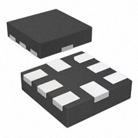
RUG PACKAGE
(TOP VIEW)
8
1
2
7
6
3
4
5
PIN #
NAME
COMMENTS
1
VCC
Supply Voltage
2
DIN
Data Input
3
GND
Ground
4
Q0
GPO
5
Q1
GPO
6
Q2
GPO
7
Q3
GPO
8
Q4
GPO
DESCRIPTION
The TCA5405 is a 5-bit output expander controlled using a single wire input. This device is ideal for portable
applications as it has a wide VCC range of 1.65V to 3.6 V. The TCA5405 uses a self-timed serial data protocol
with a single data input driven by a master device synchronized to an internal clock of that device. During a
Setup phase, the bit period is sampled, then the TCA5405 generates its own internal clock synchronized to that
of the Master device to sample the input over a five-bit-period Data Transfer phase and writes the bit states on
the parallel outputs after the last bit is sampled. The TCA5405 is available in an 8-pin 1.5mm x 1.5mm RUG
uQFN package.
ORDERING INFORMATION
TA
–40°C to 85°C
(1)
PACKAGE (1)
uQFN – RUG
Tape and Reel
ORDERABLE PART NUMBER
TOP-SIDE MARKING
TCA5405RUGR
6Y
Package drawings, standard packing quantities, thermal data, symbolization, and PCB design guidelines are available at
www.ti.com/sc/package.
1
Please be aware that an important notice concerning availability, standard warranty, and use in critical applications of Texas
Instruments semiconductor products and disclaimers thereto appears at the end of this data sheet.
PRODUCTION DATA information is current as of publication date.
Products conform to specifications per the terms of the Texas
Instruments standard warranty. Production processing does not
necessarily include testing of all parameters.
Copyright © 2011, Texas Instruments Incorporated
�TCA5405
SCPS228 – MARCH 2011
www.ti.com
These devices have limited built-in ESD protection. The leads should be shorted together or the device placed in conductive foam
during storage or handling to prevent electrostatic damage to the MOS gates.
APPLICATION DIAGRAM
VCC
Master
I/O
Q4
Q3
Q2
Q1
Q0
TCA5405
DIN
Figure 1. TCA5405 Application Diagram
ABSOLUTE MAXIMUM RATINGS (1)
over operating free-air temperature range (unless otherwise noted)
MIN
MAX
VCC
Supply voltage range
–0.5
4.0
V
VI
Input voltage range (2)
–0.5
4.0
V
(2)
–0.5
UNIT
VO
Output voltage range
4.0
V
IIK
Input clamp current
VI < 0
±20
mA
IOK
Output clamp current
VO < 0
±20
mA
IOL
Continuous output low current
VO = 0 to VCC
50
mA
IOH
Continuous output high current
VO = 0 to VCC
50
mA
200
mA
Continuous current through GND
ICC
Continuous current through VCC
ΘJA
Package thermal impedance (3)
TSTG
Storage temperature range
(1)
(2)
(3)
160
RUG package
–65
243
°C/W
150
°C
Stresses above these ratings may cause permanent damage. Exposure to absolute maximum conditions for extended periods may
degrade device reliability. These are stress ratings only, and functional operation of the device at these or any other conditions beyond
those specified is not implied.
The input negative-voltage and output voltage ratings may be exceeded if the input and output current ratings are observed.
The package thermal impedance is calculated in accordance with JESD 51-7.
RECOMMENDED OPERATING CONDITIONS
MIN
MAX
UNIT
VCC
Supply voltage
1.65
3.6
V
VIH
High-level input voltage
DIN
0.7 × VCC
VCC + 0.5
V
VIL
Low-level input voltage
DIN
–0.3
0.3 × VCC
V
IOH
High-level output current
Q0–Q4
20
mA
IOL
Low-level output current
Q0–Q4
20
mA
TA
Operating free-air temperature
85
°C
2
–40
Submit Documentation Feedback
Copyright © 2011, Texas Instruments Incorporated
Product Folder Link(s) :TCA5405
�TCA5405
SCPS228 – MARCH 2011
www.ti.com
ELECTRICAL CHARACTERISTICS
over recommended operating free-air temperature range, VCC = 1.65 V to 3.6 V (unless otherwise noted)
PARAMETER
TEST CONDITIONS
VCC
MIN
–1.2
VIK
Input diode clamp voltage
II = –18 mA
1.65 V to 3.6 V
VPOR
Power on reset voltage
VI = VCC or GND, IO = 0
1.65 V to 3.6 V
II
DIN
VI = VCC or GND
1.65 V to 3.6 V
ICC_STBY
Standby Supply Current
VI on DIN = VCC or GND, IO = 0
1.65 V to 3.6 V
ICC_ACTIVE
Active current during startup and
data transfer
CI
DIN
VI = VCC or GND
VOH
OUT-port high-level output voltage
IOH = –20 mA
TYP
MAX
1
1.4
V
±0.1
µA
2
µA
400
µA
7
pF
V
1
1.65 V to 3.6 V
6
1.65 V
1.1
2.3 V
1.7
3.6 V
2.5
V
1.65 V
VOL
OUT-port low-level output voltage
IOL = 20 mA
UNIT
0.6
2.3 V
0.3
3.6 V
0.25
V
TIMING REQUIREMENTS
over recommended operating free-air temperature range, VCC = 1.65 V to 3.6 V (unless otherwise noted)
PARAMETER
TEST CONDITIONS
VCC
MIN
tPER
DIN period
1.65 V to 3.6 V
trise
DIN rise time
1.65 V to 3.6 V
tfall
DIN fall time
1.65 V to 3.6 V
fMIN
Maximum switching frequency on DIN
1.65 V to 3.6 V
fMAX
Minimum switching frequency on DIN
1.65 V to 3.6 V
0.001
TYP
MAX
ms
100
ns
100
1
Product Folder Link(s) :TCA5405
ns
MHz
10
Submit Documentation Feedback
Copyright © 2011, Texas Instruments Incorporated
UNIT
10
kHz
3
�TCA5405
SCPS228 – MARCH 2011
www.ti.com
PRINCIPLES OF OPERATION
The TCA5405 single-wire bus device has a single-bit Data Line Bus input and has five independent parallel
push-pull buffered outputs. A single input is used to control the output state for the writing to these five outputs.
This single-wire serial interface is similar to a UART type interface but operates over a wide range of values for
the bit period.
The TCA5405 uses a self-timed serial data protocol with a single data input driven by a master device
synchronized to an internal clock of that device. During a Setup phase, the bit period is sampled, then the
TCA5405 generates its own internal clock synchronized to that of the Master device to sample the input over a
five-bit-period Data Transfer phase and writes the bit states on the parallel outputs after the last bit is sampled.
The Master output bit must be transmitted via a Totem-pole output structure to ensure proper interpretation of the
incoming serial burst.
The single-wire unidirectional interface operation is defined in Figure 2.
INTERFACE TIMING
Master
System Clock
t PER
S0
DIN
S1
S2
S3
D4
D3
Period
Sense
Startup
Phase
D2
D1
D0
Data Transfer
Phase
Internally
Generated Clock
Get
D4
Q4-Q0
Get
D3
Get
D2
Get
D1
Previous Value
Get
D0
New Value
Figure 2. Definition of Single-Wire Interface
To function correctly, the bit period (tPER) of the DIN signal must be constant over the entire data transaction.
Therefore, DIN should be driven by a stable periodic signal internal to the Master device (see Figure 2 - Master
System Clock). The bit period can be any value between 1µS and 10mS.
The TCA5405 first detects the falling transition on DIN at the beginning of the S0 period to signal the start of an
incoming data burst. Next, over the period of S1 and S2, between the two rising edges on DIN, a timer measures
the duration of S1/S2 to calculate the bit period of the incoming signal. After that, the TCA5405 uses that value to
generate its own internal clock which it uses to sample DIN as near as possible to the center of the subsequent
D4-D0 bit periods. After bit D0 is sampled, the five sampled values are sent to the Q4-Q0 outputs. At the end of
the D0 bit period, if DIN is not already high, it must be set high to signal the end of the transaction and to prepare
for the next one.
4
Submit Documentation Feedback
Copyright © 2011, Texas Instruments Incorporated
Product Folder Link(s) :TCA5405
�TCA5405
SCPS228 – MARCH 2011
www.ti.com
TYPICAL CHARACTERISTICS
TA = 25°C (unless otherwise noted)
500
1500
450
1350
1200
VCC = 3.3 V
350
ICC - Supply Current - nA
ICC - Supply Current - mA
400
300
VCC = 2.5 V
250
200
VCC = 1.8 V
150
900
VCC = 2.5 V
750
600
450
100
300
50
150
-15
10
35
TA - Temperature - °C
60
VCC = 1.8 V
0
-40
0
-40
VCC = 3.3 V
1050
85
Figure 3. Active Current vs Temperature
-15
10
35
TA - Temperature - °C
60
85
Figure 4. Standby Supply Current vs Temperature
500
1500
450
1350
TA = 25°C
ICC - Supply Current - nA
ICC - Supply Current - mA
350
TA = 85°C
300
TA = -40°C
250
200
150
1050
750
600
50
150
1.8
2.1
2.4
2.7
VCC - Supply Voltage - V
3
3.3
0
1.5
3.6
Figure 5. Active Supply Current vs Supply Voltage
1.8
2.1
2.4
2.7
VCC - Supply Voltage - V
3
3.3
3.6
Figure 6. Standby Supply Current vs Supply Voltage
50
60
VI = 1.8 V
VI = 1.65 V
45
54
TA = -40°C
35
TA = 25°C
30
TA = 85°C
25
20
15
36
24
18
5
6
500
600
TA = 85°C
30
12
200
300
400
VOL - Output Low Voltage - mV
TA = 25°C
42
10
100
TA = -40°C
48
ISINK - Sink Current - mA
40
ISINK - Sink Current - mA
TA = -40°C
450
300
0
1.5
TA = 25°C
900
100
0
0
TA = 85°C
1200
400
0
0
Figure 7. I/O Sink Current vs
Output Low Voltage VCC = 1.65V
100
200
300
400
VOL - Output Low Voltage - mV
500
Figure 8. I/O Sink Current vs
Output Low Voltage VCC = 1.8 V
Submit Documentation Feedback
Copyright © 2011, Texas Instruments Incorporated
Product Folder Link(s) :TCA5405
600
5
�TCA5405
SCPS228 – MARCH 2011
www.ti.com
TYPICAL CHARACTERISTICS (continued)
TA = 25°C (unless otherwise noted)
110
90
VI = 2.5 V
VI = 3.3 V
99
81
TA = -40°C
TA = 25°C
63
TA = 85°C
54
45
36
27
66
44
33
9
11
200
300
400
VOL - Output Low Voltage - mV
500
TA = 85°C
55
22
100
TA = 25°C
77
18
0
0
TA = -40°C
88
ISINK - Sink Current - mA
ISINK - Sink Current - mA
72
0
0
600
100
200
300
400
VOL - Output Low Voltage - mV
Figure 9. I/O Sink Current vs
Output Low Voltage VCC = 2.5V
500
600
Figure 10. I/O Sink Current vs
Output Low Voltage VCC = 3.3V
0.4
110
VI = 3.6 V
99
0.35
TA = -40°C
VOL - Output Low Voltage - V
88
ISINK - Sink Current - mA
TA = 25°C
77
TA = 85°C
66
55
44
33
0.3
VCC = 1.8 V
VCC = 2.5 V
0.25
VCC = 3.3 V
0.2
0.15
0.1
22
0.05
11
0
0
100
200
300
400
VOL - Output Low Voltage - mV
500
0
-40
600
-15
Figure 11. I/O Sink Current vs
Output Low Voltage VCC =3.6V
10
35
TA - Temperature - °C
60
85
Figure 12. I/O Low Voltage vs
Temperature VCC = 3.3V at 20 mA
50
40
VI = 1.8 V
VI = 1.65 V
45
36
TA = -40°C
32
28
TA = 85°C
24
20
16
30
20
15
8
10
4
5
100
200
300
VCC - VOH - mV
400
500
600
0
0
Figure 13. I/O Source Current vs
Output High Voltage VCC = 1.65V
6
TA = 85°C
25
12
0
0
TA = -40°C
TA = 25°C
35
ISRC - mA
ISRC - mA
40
TA = 25°C
Submit Documentation Feedback
100
200
300
VCC - VOH - mV
400
500
600
Figure 14. I/O Source Current vs
Output High Voltage VCC = 1.8V
Copyright © 2011, Texas Instruments Incorporated
Product Folder Link(s) :TCA5405
�TCA5405
SCPS228 – MARCH 2011
www.ti.com
TYPICAL CHARACTERISTICS (continued)
TA = 25°C (unless otherwise noted)
70
80
VI = 3.3 V
VI = 2.5 V
63
72
TA = -40°C
56
TA = 25°C
42
TA = 85°C
35
TA = 85°C
48
40
28
32
21
24
14
16
7
8
0
0
TA = 25°C
56
ISRC - mA
ISRC - mA
49
TA = -40°C
64
0
100
200
300
VCC - VOH - mV
400
500
600
0
Figure 15. I/O Source Current vs
Output High Voltage VCC = 2.5V
100
200
300
VCC - VOH - mV
400
500
600
Figure 16. I/O Source Current vs
Output High Voltage VCC = 3.3V
0.4
80
VI = 3.6 V
72
0.35
TA = -40°C
64
VCC = 1.8 V
0.3
ISRC - mA
VCC - VOH - mV
TA = 25°C
56
TA = 85°C
48
40
32
0.25
VCC = 2.5 V
0.2
VCC = 3.3 V
0.15
24
0.1
16
0.05
8
0
0
100
200
300
VCC - VOH - mV
400
500
600
0
-40
Figure 17. I/O Source Current vs
Output High Voltage VCC = 3.6V
-15
10
35
TA - Temperature - °C
60
Figure 18. I/O High Voltage vs
Temperature VCC = 3.3V at 20 mA
Submit Documentation Feedback
Copyright © 2011, Texas Instruments Incorporated
Product Folder Link(s) :TCA5405
85
7
�PACKAGE OUTLINE
RUG0008A
X2QFN - 0.4 mm max height
SCALE 7.500
PLASTIC QUAD FLATPACK - NO LEAD
1.55
1.45
B
A
PIN 1 INDEX AREA
1.55
1.45
C
0.4 MAX
SEATING PLANE
0.05
0.00
0.08 C
SYMM
2X
0.35
0.25
2X
4
3
2X
1
(0.15)
TYP
0.45
0.35
5
SYMM
4X 0.5
1
PIN 1 ID
(45 X0.1)
2X
7
4X
8
6X
0.4
0.3
0.25
0.15
0.3
0.2
0.1
0.05
C A
C
B
4222060/A 05/14/2015
NOTES:
1. All linear dimensions are in millimeters. Any dimensions in parenthesis are for reference only. Dimensioning and tolerancing
per ASME Y14.5M.
2. This drawing is subject to change without notice.
www.ti.com
�EXAMPLE BOARD LAYOUT
RUG0008A
X2QFN - 0.4 mm max height
PLASTIC QUAD FLATPACK - NO LEAD
2X (0.3)
2X (0.6)
8
6X (0.55)
1
7
4X (0.25)
SYMM
4X (0.5)
(1.3)
2X (0.2)
3
5
(R0.05) TYP
4
SYMM
(1.35)
LAND PATTERN EXAMPLE
SCALE:25X
0.07 MAX
ALL AROUND
0.07 MIN
ALL AROUND
SOLDER MASK
OPENING
METAL
SOLDER MASK
OPENING
NON SOLDER MASK
DEFINED
(PREFERRED)
METAL
UNDER
SOLDER MASK
SOLDER MASK
DEFINED
SOLDER MASK DETAILS
NOT TO SCALE
4222060/A 05/14/2015
NOTES: (continued)
3. For more information, see Texas Instruments literature number SLUA271 (www.ti.com/lit/slua271).
www.ti.com
�EXAMPLE STENCIL DESIGN
RUG0008A
X2QFN - 0.4 mm max height
PLASTIC QUAD FLATPACK - NO LEAD
2X (0.3)
2X (0.6)
8
6X (0.55)
1
7
4X (0.25)
SYMM
4X (0.5)
(1.3)
2X (0.2)
3
5
4
SYMM
(1.35)
SOLDER PASTE EXAMPLE
BASED ON 0.1 mm THICKNESS
SCALE:25X
4222060/A 05/14/2015
NOTES: (continued)
4. Laser cutting apertures with trapezoidal walls and rounded corners may offer better paste release. IPC-7525 may have alternate
design recommendations.
www.ti.com
�PACKAGE OPTION ADDENDUM
www.ti.com
10-Dec-2020
PACKAGING INFORMATION
Orderable Device
Status
(1)
Package Type Package Pins Package
Drawing
Qty
Eco Plan
(2)
Lead finish/
Ball material
MSL Peak Temp
Op Temp (°C)
Device Marking
(3)
(4/5)
(6)
TCA5405RUGR
ACTIVE
X2QFN
RUG
8
3000
RoHS & Green
NIPDAUAG
Level-1-260C-UNLIM
-40 to 85
6Y
(1)
The marketing status values are defined as follows:
ACTIVE: Product device recommended for new designs.
LIFEBUY: TI has announced that the device will be discontinued, and a lifetime-buy period is in effect.
NRND: Not recommended for new designs. Device is in production to support existing customers, but TI does not recommend using this part in a new design.
PREVIEW: Device has been announced but is not in production. Samples may or may not be available.
OBSOLETE: TI has discontinued the production of the device.
(2)
RoHS: TI defines "RoHS" to mean semiconductor products that are compliant with the current EU RoHS requirements for all 10 RoHS substances, including the requirement that RoHS substance
do not exceed 0.1% by weight in homogeneous materials. Where designed to be soldered at high temperatures, "RoHS" products are suitable for use in specified lead-free processes. TI may
reference these types of products as "Pb-Free".
RoHS Exempt: TI defines "RoHS Exempt" to mean products that contain lead but are compliant with EU RoHS pursuant to a specific EU RoHS exemption.
Green: TI defines "Green" to mean the content of Chlorine (Cl) and Bromine (Br) based flame retardants meet JS709B low halogen requirements of
很抱歉,暂时无法提供与“TCA5405RUGR”相匹配的价格&库存,您可以联系我们找货
免费人工找货