User's Guide
SLVUAA2 – August 2014
TCA8418E Keypad Scan EVM
This user’s guide describes the TCA8418E-EVM keypad scan evaluation module (EVM). This guide
contains an introduction, setup instructions, the EVM schematic, top and bottom board layouts, and a bill
of materials (BOM).
6
7
8
Contents
Information About Cautions and Warnings ............................................................................... 2
Items Required for Operation .............................................................................................. 2
Items Recommended for Operation ....................................................................................... 2
Introduction ................................................................................................................... 2
Setup .......................................................................................................................... 4
5.1
Header/Jumper Connections Description........................................................................ 4
5.2
LaunchPad Hardware/Firmware Setup ......................................................................... 5
5.3
GUI Software Setup ................................................................................................ 9
5.4
Default Register Settings in the TCA8418E when Using the LaunchPad ................................. 10
5.5
Getting Started Using the TCA8418E-EVM.................................................................... 11
Schematic ................................................................................................................... 14
Board Layout ................................................................................................................ 15
Bill of Materials ............................................................................................................. 19
1
TCA8418E-EVM ............................................................................................................. 3
2
Header J5 Connections to TCA8418E Pins (Top View) ................................................................ 4
3
Proper Jumper Configuration on the LaunchPad ........................................................................ 5
4
Proper Orientation for the TCA8418E-EVM on the LaunchPad.
5
Opening Device Manager in Windows .................................................................................... 6
6
Updating Driver Software in Device Manager ............................................................................ 7
7
Browsing for the Driver Software .......................................................................................... 7
8
Successful Installation of the MSP430 LaunchPad Drivers ............................................................ 7
9
Flashing the MSP430
10
Successfully Flashed MSP430 ............................................................................................. 8
11
Installing the TCA8418E-EVM GUI ........................................................................................ 9
12
TCA8418E-EVM GUI After Connecting the LaunchPad to the Computer
13
TCA8418E-EVM GUI After Connecting the LaunchPad to the Computer .......................................... 11
14
Key Press Matrix Display While Holding Down the Middle Button (SW12)......................................... 12
15
Main Configuration and Input Register Display
16
Reading Register 0x0E .................................................................................................... 13
17
Result of Reading Register 0x0E
18
Writing 0xA6 to Register 0x0E............................................................................................ 13
19
Result of Writing 0xA6 to Register 0x0E ................................................................................ 13
20
TCA8418E-EVM Schematic
21
PCB Layer 1 (Top Layer).................................................................................................. 15
22
PCB Layer 2 (GND) ........................................................................................................ 16
23
PCB Layer 3 (VCC) ........................................................................................................ 17
1
2
3
4
5
List of Figures
......................................................
.......................................................................................................
...........................................
........................................................................
........................................................................................
..............................................................................................
SLVUAA2 – August 2014
Submit Documentation Feedback
TCA8418E Keypad Scan EVM
Copyright © 2014, Texas Instruments Incorporated
6
7
9
12
13
14
1
�Information About Cautions and Warnings
24
www.ti.com
PCB Layer 4 (Bottom Layer) .............................................................................................. 18
List of Tables
1
1
Device and Package Configurations ...................................................................................... 3
2
Default TCA8418E Register Values When Using the LaunchPad ................................................... 10
3
Bill of Materials
.............................................................................................................
19
Information About Cautions and Warnings
CAUTION
This EVM contains components that can potentially be damaged by
electrostatic discharge. Always transport and store the EVM in its supplied ESD
bag when not in use. Handle using an antistatic wristband. Operate on an
antistatic work surface. For more information on proper handling, see the
Electrostatic Discharge (ESD) application note (SSYA008).
The information in a caution or a warning is provided for your protection. Read each caution and warning
carefully.
2
Items Required for Operation
The following items are required to use the TCA8418E-EVM:
• TCA8418E-EVM
• TCA8418E datasheet (SCPS222)
• One power supply for VCC
– 3.3 V at 100 mA recommended
3
Items Recommended for Operation
The following items are recommended for use with the TCA8418E-EVM:
• MSP430 LaunchPad
– Recommended rev 1.5
– MSP430G2553 installed
• USB standard-A to mini-B cable
• Computer running Microsoft® Windows® 7 with 1 available USB port
4
Introduction
This document is the user’s guide for the TCA8418E-EVM. The TCA8418E-EVM can be used as a
standalone system or paired with the MSP-EXP430G2 LaunchPad to facilitate power and I2C
communication. When paired with the LaunchPad, The TCA8418E-EVM GUI can be used to read from or
write to internal registers of the TCA8418E keypad scan IC, allowing the user to control the states of the
I/O pins as well as see key presses in real-time.
Microsoft, Windows are registered trademarks of Microsoft Corporation.
2
TCA8418E Keypad Scan EVM
SLVUAA2 – August 2014
Submit Documentation Feedback
Copyright © 2014, Texas Instruments Incorporated
�Introduction
www.ti.com
Table 1. Device and Package Configurations
Keypad Scan IC
IC
Package
U1
TCA8418EYFFR
DSBGA-32
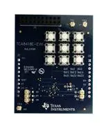
Figure 1. TCA8418E-EVM
SLVUAA2 – August 2014
Submit Documentation Feedback
TCA8418E Keypad Scan EVM
Copyright © 2014, Texas Instruments Incorporated
3
�Setup
5
www.ti.com
Setup
This section describes the header/jumper connections on the TCA8418E-EVM, installation of the firmware
on the MSP430 LaunchPad, installation of the software (GUI) on the computer, and getting started using
the TCA8418E-EVM with any of the supported devices.
5.1
5.1.1
Header/Jumper Connections Description
TP1: Power Input
Test point TP1 allows power input without the LaunchPad. The range is 1.65 V to 3.6 V.
5.1.2
TP2 and TP3: Ground
Test points TP2 and TP3 are connected to ground.
5.1.3
J1 and J2: MSP430 LaunchPad Interface Headers
Headers J1 and J2 are the connectors for the MSP430 LaunchPad to the TCA8418E-EVM.
5.1.4
J3: I2C Test Points
Header J3 is a test point for SDA and SCL, and allows I2C input when the LaunchPad is not present.
5.1.5
J4: RESET and Interrupt Test Points
Test point J4 is a test point for the RESET input, INT output, and CAD_INT output.
5.1.6
J5: Keypad Extension Header
Header J5 allows extension of the functionality of the TCA8418E-EVM onto a larger keypad or GPIO
expander board.
COL9
COL8
COL7
COL6
COL5
COL4
COL3
COL2
COL1
COL0
GND
VCC
ROW7
ROW6
ROW5
ROW4
ROW3
ROW2
ROW1
ROW0
J5
Figure 2. Header J5 Connections to TCA8418E Pins (Top View)
5.1.7
SW1, SW2, SW3, SW11, SW12, SW13, SW21, SW22, SW23: Keypad Switches
These switches are named in accordance with the Key Value Assignment table in the TCA8418E
(SCPS222) datasheet. They are for ROW0-ROW2 and COL0-COL2, which are programmed as keypad
I/Os, by default, on the TCA8418E-EVM.
4
TCA8418E Keypad Scan EVM
SLVUAA2 – August 2014
Submit Documentation Feedback
Copyright © 2014, Texas Instruments Incorporated
�Setup
www.ti.com
5.2
LaunchPad Hardware/Firmware Setup
If using the TCA8418E-EVM GUI, the MSP430 LaunchPad board needs to be configured properly in order
to flash the processor with the TCA8418E-EVM firmware. Implement the following steps before using the
TCA8418E-EVM in conjunction with the LaunchPad:
1. With the LaunchPad unplugged, configure the headers on the LaunchPad to be in HW UART mode by
attaching jumpers on the headers indicated by the yellow boxes in Figure 3.
Figure 3. Proper Jumper Configuration on the LaunchPad
SLVUAA2 – August 2014
Submit Documentation Feedback
TCA8418E Keypad Scan EVM
Copyright © 2014, Texas Instruments Incorporated
5
�Setup
www.ti.com
2. Place the TCA8418E-EVM on top of the LaunchPad so that all connectors on J1 and J2 of the
LaunchPad are inserted into J1 and J2 of the TCA8418E-EVM and J7 on the TCA8418E-EVM is on
the same side as the mini-USB connector of the LaunchPad.
Figure 4. Proper Orientation for the TCA8418E-EVM on the LaunchPad.
3. Download the firmware (for the MSP430) and software (graphical user interface, or GUI) in a zipped
folder (SLVC601) located on the TCA8418E-EVM webpage on ti.com.
4. Right-click on the zip folder and select Extract All.
5. Click Extract.
6. Plug in the MSP430 LaunchPad to the computer.
7. Open Device Manager (Type “devmgmt.msc” into the Start menu and hit Enter):
Figure 5. Opening Device Manager in Windows
8. Select the MSP430 Application (see Figure 6), right click → Properties, and click Update Driver
Software. The MSP430 Application may appear either in Ports or Other Devices.
6
TCA8418E Keypad Scan EVM
SLVUAA2 – August 2014
Submit Documentation Feedback
Copyright © 2014, Texas Instruments Incorporated
�Setup
www.ti.com
Figure 6. Updating Driver Software in Device Manager
9. Select Browse my computer.
Figure 7. Browsing for the Driver Software
10. Select the folder where you extracted [SLVC601].zip.
11. Click Next. Click Close after you see the following:
Figure 8. Successful Installation of the MSP430 LaunchPad Drivers
12. Flash the MSP430 by double-clicking TCA8418E_Flasher.bat in the TCA8418E-EVM LaunchPad Files
folder where you extracted [SLVC601].zip.
Figure 9. Flashing the MSP430
SLVUAA2 – August 2014
Submit Documentation Feedback
TCA8418E Keypad Scan EVM
Copyright © 2014, Texas Instruments Incorporated
7
�Setup
www.ti.com
13. Verify that the command window says “no errors” and then press any key to close the window. A
successful flash of the firmware results in the following command line prompt:
Figure 10. Successfully Flashed MSP430
14. Press any key to continue.
8
TCA8418E Keypad Scan EVM
SLVUAA2 – August 2014
Submit Documentation Feedback
Copyright © 2014, Texas Instruments Incorporated
�Setup
www.ti.com
5.3
GUI Software Setup
1. Run setup.exe, located in the TCA8418E_GUI folder. From now on, the TCA8418E software is
available under the Start menu in Programs → Texas Instruments, Inc → TCA8418E.exe.
Figure 11. Installing the TCA8418E-EVM GUI
2. If the GUI does not launch automatically, run the installed TCA8418E-EVM GUI program from the Start
menu.
3. The GUI looks like the following image when it is opened and the LaunchPad is connected:
Figure 12. TCA8418E-EVM GUI After Connecting the LaunchPad to the Computer
SLVUAA2 – August 2014
Submit Documentation Feedback
TCA8418E Keypad Scan EVM
Copyright © 2014, Texas Instruments Incorporated
9
�Setup
5.4
www.ti.com
Default Register Settings in the TCA8418E when Using the LaunchPad
Upon startup, the MSP430 LaunchPad configures the TCA8418E to work as a keypad scanner with the
following values:
Table 2. Default TCA8418E Register Values When Using the LaunchPad
10
Register
Register Name
Default Value for EVM
Comment
0x00
Reserved
0x97
Interrupts enabled (except Overflow)
0x01
CFG
0x00
0x02
INT_STAT
0x00
0x03
KEY_LCK_EC
0x00
0x04
KEY_EVENT_A
0x00
0x05
KEY_EVENT_B
0x00
0x06
KEY_EVENT_C
0x00
0x07
KEY_EVENT_D
0x00
0x08
KEY_EVENT_E
0x00
0x09
KEY_EVENT_F
0x00
0x0A
KEY_EVENT_G
0x00
0x0B
KEY_EVENT_H
0x00
0x0C
KEY_EVENT_I
0x00
0x0D
KEY_EVENT_J
0x00
0x0E
KP_LCK_TIMER
0xA7
0x0F
Unlock1
0x0C
Key #12
0x10
Unlock2
0x0C
Key #12 – Press twice to unlock
0x11
GPIO_INT_STAT1
0x00
0x12
GPIO_INT_STAT2
0x00
0x13
GPIO_INT_STAT3
0x00
0x14
GPIO_DAT_STAT1
0xFF
0x15
GPIO_DAT_STAT2
0xFF
0x16
GPIO_DAT_STAT3
0x03
0x17
GPIO_DAT_OUT1
0x00
0x18
GPIO_DAT_OUT2
0x00
0x19
GPIO_DAT_OUT3
0x00
0x1A
GPIO_INT_EN1
0x00
0x1B
GPIO_INT_EN2
0x00
0x1C
GPIO_INT_EN3
0x00
0x1D
KP_GPIO1
0xFF
ROW0 through ROW7: keypad scan
0x1E
KP_GPIO2
0xFF
COL0 through COL7: keypad scan
0x1F
KP_GPIO3
0x00
0x20
GPI_EM1
0x00
0x21
GPI_EM2
0x00
0x22
GPI_EM3
0x00
0x23
GPIO_DIR1
0x00
0x24
GPIO_DIR2
0x00
0x25
GPIO_DIR3
0x00
0x26
GPIO_INT_LVL_1
0x00
0x27
GPIO_INT_LVL_2
0x00
0x28
GPIO_INT_LVL_3
0x00
0x29
DEBOUNCE_DIS_1
0x00
0x2A
DEBOUNCE_DIS_2
0x00
0x2B
DEBOUNCE_DIS_3
0x00
TCA8418E Keypad Scan EVM
SLVUAA2 – August 2014
Submit Documentation Feedback
Copyright © 2014, Texas Instruments Incorporated
�Setup
www.ti.com
Table 2. Default TCA8418E Register Values When Using the LaunchPad (continued)
Register
Register Name
Default Value for EVM
0x2C
GPIO_PULL1
0x00
0x2D
GPIO_PULL2
0x00
0x2E
GPIO_PULL3
0x00
Comment
5.5
Getting Started Using the TCA8418E-EVM
5.5.1
Evaluating the TCA8418E EVM without the LaunchPad
1. To power the TCA8418E-EVM without the LaunchPad, apply a 3.3-V, 100-mA power supply to TP1
(VCC pin). Although 3.3 V is preferred, the voltage range can be from 1.65 V to 3.6 V.
2. Attach an external microcontroller to J3 to provide SCL and SDA inputs for I2C. Keep in mind that SCL
and SDA are pulled up to VCC on the TCA8418E-EVM through 4.7-kΩ resistors. Therefore, using the
same power supply for the microcontroller and the TCA8418E-EVM is recommended.
3. Use the built-in 3x3 keypad on the TCA8418E-EVM or use J5 to attach an external keypad. If attaching
an external keypad, the KP_GPIO registers (0x1D, 0x1E, and 0x1F) should be configured to
accommodate the additional keys.
5.5.2
Evaluating the TCA8418E EVM with the LaunchPad
After completing the steps in Section 5.2, launch the TCA8418E-EVM software. The screen will look like
Figure 13.
Figure 13. TCA8418E-EVM GUI After Connecting the LaunchPad to the Computer
SLVUAA2 – August 2014
Submit Documentation Feedback
TCA8418E Keypad Scan EVM
Copyright © 2014, Texas Instruments Incorporated
11
�Setup
www.ti.com
5.5.2.1
Using the Key Press Matrix Display
Connect the TCA8418E-EVM and launch the GUI. The key press matrix display will only work when
KE_IEN (0x01, bit 0) is set to 1. By default, key event interrupts are enabled because KE_IEN (0x01, bit 0)
is set to 1 and the key press matrix display responds in real-time to key presses and releases. Press the
middle button (SW12) on the TCA8418E-EVM and observe the feedback from the display (Figure 14).
Figure 14. Key Press Matrix Display While Holding Down the Middle Button (SW12)
Releasing the key causes the grey box to become white again.
5.5.2.2
Main Configuration and Input Registers
Figure 15. Main Configuration and Input Register Display
The main configuration and input registers are the registers most likely to change while operating the
TCA8418E-EVM. For this reason, they are more prominent on the GUI.
The CFG register contains the interrupt enable bits for different types of interrupts.
The INT_STAT register contains the actual state of each type of interrupt.
The KEY_LCK_EC contains the lock status, can be written to lock the keypad, and counts the number of
key events (in the 4 least significant bits).
KEY_EVENT_A is the top of the first-in first-out (FIFO) stack that records key presses and releases.
KEY_EVENT_A is read automatically when KE_IEN = 1 and a key has been pressed or released.
Whenever one of these four registers is read, the main configuration and input register display updates to
show the newly read value of those registers.
The Read registers 1-4 every second checkbox causes the TCA8418E-EVM GUI to start a timer that will
read registers 1 through 4 every second. The read takes 100 ms. This feature shows how KEY_EVENT_A
and KEY_LCK_EC change every time the registers are read. Disable the KE_IEN bit before checking this
box; otherwise, nothing appears to occur in registers 3 and 4.
12
TCA8418E Keypad Scan EVM
SLVUAA2 – August 2014
Submit Documentation Feedback
Copyright © 2014, Texas Instruments Incorporated
�Setup
www.ti.com
5.5.2.3
Reading and Writing Registers
All registers in the TCA8418E can be read using the TCA8418E-EVM GUI. Figure 16 shows how to read
register 0x0E:
Figure 16. Reading Register 0x0E
Click the Read Register button and the following appears in the activity log text (Figure 17):
Figure 17. Result of Reading Register 0x0E
Similarly, any register can be written as well. Figure 18 shows how to write 0xA6 to register 0x0E:
Figure 18. Writing 0xA6 to Register 0x0E
The activity log reflects the newly written register:
Figure 19. Result of Writing 0xA6 to Register 0x0E
SLVUAA2 – August 2014
Submit Documentation Feedback
TCA8418E Keypad Scan EVM
Copyright © 2014, Texas Instruments Incorporated
13
�Schematic
6
www.ti.com
Schematic
Figure 20 shows the schematic for the TCA8418E-EVM.
1
2
3
4
5
6
VCC
TP1
VCC is power input to the board. Range is 1.65 V to 3.6 V.
C1
�)
C2
���)
A
A
GND
GND
VCC
J1
P1.0
P1.1
P1.2
P1.3
RESET
INT
CAD_INT
P2.1
P2.2
J2
1
2
3
4
5
6
7
8
9
10
XIN
XOUT
TST
RST
SDA
SCL
P2.5
P2.4
P2.3
GND
1
2
3
4
5
6
7
8
9
10
U1
VCC
B5
SCL
SDA
D5
C5
RESET A5
B
VCC
SCL
SDA
RESET
VCC
CAD_INT B2
R1
4.7k
R2
4.7k
INT
J3
E5
CAD_INT
INT
SDA
SCL
COL0
COL1
COL2
COL3
COL4
COL5
COL6
COL7
COL8
COL9
ROW0
ROW1
ROW2
ROW3
ROW4
ROW5
ROW6
ROW7
GND
E2
A3
B3
C3
D3
E3
A4
B4
C4
D4
COL0
COL1
COL2
COL3
COL4
COL5
COL6
COL7
COL8
COL9
D2
C2
A2
E1
D1
C1
B1
A1
ROW0
ROW1
ROW2
ROW3
ROW4
ROW5
ROW6
ROW7
COL0
COL1
COL2
SW1
1
2
SW2
4
3
1
2
SW3
4
3
1
2
4
3
B
ROW0
SW11
1
2
SW12
4
3
1
2
4
3
1
2
SW13
4
3
1
2
4
3
1
2
4
3
ROW1
E4
SW21
TCA8418EYFPR
SW22
SW23
GND
VCC
R3
10k
1
2
R4
10k
R5
10k
4
3
ROW2
J4
RESET
INT
CAD_INT
Switch designators named to match Key Value Assignment table in TCA8418E datasheet.
C
C
TP2
GND
TP3
GND
J5
D
COL0
COL1
COL2
COL3
COL4
COL5
COL6
COL7
COL8
COL9
2
4
6
8
10
12
14
16
18
20
1
3
5
7
9
11
13
15
17
19
ROW0
ROW1
ROW2
ROW3
ROW4
ROW5
ROW6
ROW7
VCC
GND
D
Number: HVL049
Rev: A
Texas Instruments and/or its licensors do not warrant the accuracy or completeness of this specification or any information contained therein. Texas Instruments and/or its licensors do no SVN Rev: Not in version control
warrant that this design will meet the specifications, will be suitable for your application or fit for any particular purpose, or will operate in an implementation. Texas Instruments and/or its Drawn By:
licensors do not warrant that the design is production worthy. You should completely validate and test your design implementation to confirm the system functionality for your application. Engineer: Ryan Land
1
2
3
4
5
Designed for: Public Release
Mod. Date: 7/22/2014
Project Title: TCA8418E-EVM
Sheet Title:
Assembly Variant: Variant name not interpreted Sheet: 1 of 1
File: HVL049A.SchDoc
Size: B
Contact: http://www.ti.com/support
http://www.ti.com
�7H[DV�,QVWUXPHQWV 2014
6
Figure 20. TCA8418E-EVM Schematic
14
TCA8418E Keypad Scan EVM
SLVUAA2 – August 2014
Submit Documentation Feedback
Copyright © 2014, Texas Instruments Incorporated
�Board Layout
www.ti.com
7
Board Layout
Figure 21. PCB Layer 1 (Top Layer)
SLVUAA2 – August 2014
Submit Documentation Feedback
TCA8418E Keypad Scan EVM
Copyright © 2014, Texas Instruments Incorporated
15
�Board Layout
www.ti.com
Figure 22. PCB Layer 2 (GND)
16
TCA8418E Keypad Scan EVM
SLVUAA2 – August 2014
Submit Documentation Feedback
Copyright © 2014, Texas Instruments Incorporated
�Board Layout
www.ti.com
Figure 23. PCB Layer 3 (VCC)
SLVUAA2 – August 2014
Submit Documentation Feedback
TCA8418E Keypad Scan EVM
Copyright © 2014, Texas Instruments Incorporated
17
�Board Layout
www.ti.com
Figure 24. PCB Layer 4 (Bottom Layer)
18
TCA8418E Keypad Scan EVM
SLVUAA2 – August 2014
Submit Documentation Feedback
Copyright © 2014, Texas Instruments Incorporated
�Bill of Materials
www.ti.com
8
Bill of Materials
Table 3 lists the BOM for this EVM.
Table 3. Bill of Materials
Designator
Value
Description
Package Reference
Part Number
Manufacturer
C1
Qty
1
1µF
CAP, CERM, 1µF, 16V, ±10%, X5R,
0603
603
GRM188R61C105KA93D
Murata
C2
1
0.1µF
CAP, CERM, 0.1µF, 16V, ±10%,
X7R, 0402
402
GRM155R71C104KA88D
Murata
J1, J2
2
Receptacle 100mil 10x1, Tin, TH
Receptacle, 10x1, 100mil,
Tin
PPTC101LFBN-RC
Sullins Connector
Solutions
J3
1
Header, 100mil, 2x1, Gold plated, TH
Header, 2x1, 100mil
J4
1
J5
5-146261-1
TE Connectivity
Header, TH, 100mil, 1x3, Gold plated, PBC03SAAN
230 mil above insulator
PBC03SAAN
Sullins Connector
Solutions
1
Receptacle, 10x2, 100mil, TH
10x2 Receptacle
PPPC102LFBN-RC
Sullins Connector
Solutions
LBL1
1
Thermal Transfer Printable Labels,
1.250" W x 0.250" H - 10,000 per roll
PCB Label 1.25"H x
0.250"W
THT-13-457-10
Brady
R1, R2
2
4.7k
RES, 4.7kΩ, 5%, 0.1W, 0603
603
CRCW06034K70JNEA
Vishay-Dale
R3, R4, R5
3
10k
RES, 10kΩ, 5%, 0.1W, 0603
603
CRCW060310K0JNEA
Vishay-Dale
SW1–SW3,
SW11–SW13,
SW21–SW23
9
SWITCH TACTILE SPST-NO 0.02A
15V, TH
6x4.3x6mm
EVQ-PAD04M
Panasonic
TP1, TP2, TP3
3
Header, 100mil, 1pos, Gold, TH
Testpoint
TSW-101-07-G-S
Samtec
U1
1
I2C CONTROLLED KEYPAD SCAN
IC WITH INTEGRATED ESD
PROTECTION, YFP0025ABAB
YFP0025ABAB
TCA8418EYFPR
Texas Instruments
1x3
SLVUAA2 – August 2014
Submit Documentation Feedback
TCA8418E Keypad Scan EVM
Copyright © 2014, Texas Instruments Incorporated
19
�ADDITIONAL TERMS AND CONDITIONS, WARNINGS, RESTRICTIONS, AND DISCLAIMERS FOR
EVALUATION MODULES
Texas Instruments Incorporated (TI) markets, sells, and loans all evaluation boards, kits, and/or modules (EVMs) pursuant to, and user
expressly acknowledges, represents, and agrees, and takes sole responsibility and risk with respect to, the following:
1.
User agrees and acknowledges that EVMs are intended to be handled and used for feasibility evaluation only in laboratory and/or
development environments. Notwithstanding the foregoing, in certain instances, TI makes certain EVMs available to users that do not
handle and use EVMs solely for feasibility evaluation only in laboratory and/or development environments, but may use EVMs in a
hobbyist environment. All EVMs made available to hobbyist users are FCC certified, as applicable. Hobbyist users acknowledge, agree,
and shall comply with all applicable terms, conditions, warnings, and restrictions in this document and are subject to the disclaimer and
indemnity provisions included in this document.
2. Unless otherwise indicated, EVMs are not finished products and not intended for consumer use. EVMs are intended solely for use by
technically qualified electronics experts who are familiar with the dangers and application risks associated with handling electrical
mechanical components, systems, and subsystems.
3. User agrees that EVMs shall not be used as, or incorporated into, all or any part of a finished product.
4. User agrees and acknowledges that certain EVMs may not be designed or manufactured by TI.
5. User must read the user's guide and all other documentation accompanying EVMs, including without limitation any warning or
restriction notices, prior to handling and/or using EVMs. Such notices contain important safety information related to, for example,
temperatures and voltages. For additional information on TI's environmental and/or safety programs, please visit www.ti.com/esh or
contact TI.
6. User assumes all responsibility, obligation, and any corresponding liability for proper and safe handling and use of EVMs.
7. Should any EVM not meet the specifications indicated in the user’s guide or other documentation accompanying such EVM, the EVM
may be returned to TI within 30 days from the date of delivery for a full refund. THE FOREGOING LIMITED WARRANTY IS THE
EXCLUSIVE WARRANTY MADE BY TI TO USER AND IS IN LIEU OF ALL OTHER WARRANTIES, EXPRESSED, IMPLIED, OR
STATUTORY, INCLUDING ANY WARRANTY OF MERCHANTABILITY OR FITNESS FOR ANY PARTICULAR PURPOSE. TI SHALL
NOT BE LIABLE TO USER FOR ANY INDIRECT, SPECIAL, INCIDENTAL, OR CONSEQUENTIAL DAMAGES RELATED TO THE
HANDLING OR USE OF ANY EVM.
8. No license is granted under any patent right or other intellectual property right of TI covering or relating to any machine, process, or
combination in which EVMs might be or are used. TI currently deals with a variety of customers, and therefore TI’s arrangement with
the user is not exclusive. TI assumes no liability for applications assistance, customer product design, software performance, or
infringement of patents or services with respect to the handling or use of EVMs.
9. User assumes sole responsibility to determine whether EVMs may be subject to any applicable federal, state, or local laws and
regulatory requirements (including but not limited to U.S. Food and Drug Administration regulations, if applicable) related to its handling
and use of EVMs and, if applicable, compliance in all respects with such laws and regulations.
10. User has sole responsibility to ensure the safety of any activities to be conducted by it and its employees, affiliates, contractors or
designees, with respect to handling and using EVMs. Further, user is responsible to ensure that any interfaces (electronic and/or
mechanical) between EVMs and any human body are designed with suitable isolation and means to safely limit accessible leakage
currents to minimize the risk of electrical shock hazard.
11. User shall employ reasonable safeguards to ensure that user’s use of EVMs will not result in any property damage, injury or death,
even if EVMs should fail to perform as described or expected.
12. User shall be solely responsible for proper disposal and recycling of EVMs consistent with all applicable federal, state, and local
requirements.
Certain Instructions. User shall operate EVMs within TI’s recommended specifications and environmental considerations per the user’s
guide, accompanying documentation, and any other applicable requirements. Exceeding the specified ratings (including but not limited to
input and output voltage, current, power, and environmental ranges) for EVMs may cause property damage, personal injury or death. If
there are questions concerning these ratings, user should contact a TI field representative prior to connecting interface electronics including
input power and intended loads. Any loads applied outside of the specified output range may result in unintended and/or inaccurate
operation and/or possible permanent damage to the EVM and/or interface electronics. Please consult the applicable EVM user's guide prior
to connecting any load to the EVM output. If there is uncertainty as to the load specification, please contact a TI field representative. During
normal operation, some circuit components may have case temperatures greater than 60°C as long as the input and output are maintained
at a normal ambient operating temperature. These components include but are not limited to linear regulators, switching transistors, pass
transistors, and current sense resistors which can be identified using EVMs’ schematics located in the applicable EVM user's guide. When
placing measurement probes near EVMs during normal operation, please be aware that EVMs may become very warm. As with all
electronic evaluation tools, only qualified personnel knowledgeable in electronic measurement and diagnostics normally found in
development environments should use EVMs.
Agreement to Defend, Indemnify and Hold Harmless. User agrees to defend, indemnify, and hold TI, its directors, officers, employees,
agents, representatives, affiliates, licensors and their representatives harmless from and against any and all claims, damages, losses,
expenses, costs and liabilities (collectively, "Claims") arising out of, or in connection with, any handling and/or use of EVMs. User’s
indemnity shall apply whether Claims arise under law of tort or contract or any other legal theory, and even if EVMs fail to perform as
described or expected.
Safety-Critical or Life-Critical Applications. If user intends to use EVMs in evaluations of safety critical applications (such as life support),
and a failure of a TI product considered for purchase by user for use in user’s product would reasonably be expected to cause severe
personal injury or death such as devices which are classified as FDA Class III or similar classification, then user must specifically notify TI
of such intent and enter into a separate Assurance and Indemnity Agreement.
�RADIO FREQUENCY REGULATORY COMPLIANCE INFORMATION FOR EVALUATION MODULES
Texas Instruments Incorporated (TI) evaluation boards, kits, and/or modules (EVMs) and/or accompanying hardware that is marketed, sold,
or loaned to users may or may not be subject to radio frequency regulations in specific countries.
General Statement for EVMs Not Including a Radio
For EVMs not including a radio and not subject to the U.S. Federal Communications Commission (FCC) or Industry Canada (IC)
regulations, TI intends EVMs to be used only for engineering development, demonstration, or evaluation purposes. EVMs are not finished
products typically fit for general consumer use. EVMs may nonetheless generate, use, or radiate radio frequency energy, but have not been
tested for compliance with the limits of computing devices pursuant to part 15 of FCC or the ICES-003 rules. Operation of such EVMs may
cause interference with radio communications, in which case the user at his own expense will be required to take whatever measures may
be required to correct this interference.
General Statement for EVMs including a radio
User Power/Frequency Use Obligations: For EVMs including a radio, the radio included in such EVMs is intended for development and/or
professional use only in legally allocated frequency and power limits. Any use of radio frequencies and/or power availability in such EVMs
and their development application(s) must comply with local laws governing radio spectrum allocation and power limits for such EVMs. It is
the user’s sole responsibility to only operate this radio in legally acceptable frequency space and within legally mandated power limitations.
Any exceptions to this are strictly prohibited and unauthorized by TI unless user has obtained appropriate experimental and/or development
licenses from local regulatory authorities, which is the sole responsibility of the user, including its acceptable authorization.
U.S. Federal Communications Commission Compliance
For EVMs Annotated as FCC – FEDERAL COMMUNICATIONS COMMISSION Part 15 Compliant
Caution
This device complies with part 15 of the FCC Rules. Operation is subject to the following two conditions: (1) This device may not cause
harmful interference, and (2) this device must accept any interference received, including interference that may cause undesired operation.
Changes or modifications could void the user's authority to operate the equipment.
FCC Interference Statement for Class A EVM devices
This equipment has been tested and found to comply with the limits for a Class A digital device, pursuant to part 15 of the FCC Rules.
These limits are designed to provide reasonable protection against harmful interference when the equipment is operated in a commercial
environment. This equipment generates, uses, and can radiate radio frequency energy and, if not installed and used in accordance with the
instruction manual, may cause harmful interference to radio communications. Operation of this equipment in a residential area is likely to
cause harmful interference in which case the user will be required to correct the interference at its own expense.
FCC Interference Statement for Class B EVM devices
This equipment has been tested and found to comply with the limits for a Class B digital device, pursuant to part 15 of the FCC Rules.
These limits are designed to provide reasonable protection against harmful interference in a residential installation. This equipment
generates, uses and can radiate radio frequency energy and, if not installed and used in accordance with the instructions, may cause
harmful interference to radio communications. However, there is no guarantee that interference will not occur in a particular installation. If
this equipment does cause harmful interference to radio or television reception, which can be determined by turning the equipment off and
on, the user is encouraged to try to correct the interference by one or more of the following measures:
• Reorient or relocate the receiving antenna.
• Increase the separation between the equipment and receiver.
• Connect the equipment into an outlet on a circuit different from that to which the receiver is connected.
• Consult the dealer or an experienced radio/TV technician for help.
Industry Canada Compliance (English)
For EVMs Annotated as IC – INDUSTRY CANADA Compliant:
This Class A or B digital apparatus complies with Canadian ICES-003.
Changes or modifications not expressly approved by the party responsible for compliance could void the user’s authority to operate the
equipment.
Concerning EVMs Including Radio Transmitters
This device complies with Industry Canada licence-exempt RSS standard(s). Operation is subject to the following two conditions: (1) this
device may not cause interference, and (2) this device must accept any interference, including interference that may cause undesired
operation of the device.
Concerning EVMs Including Detachable Antennas
Under Industry Canada regulations, this radio transmitter may only operate using an antenna of a type and maximum (or lesser) gain
approved for the transmitter by Industry Canada. To reduce potential radio interference to other users, the antenna type and its gain should
be so chosen that the equivalent isotropically radiated power (e.i.r.p.) is not more than that necessary for successful communication.
This radio transmitter has been approved by Industry Canada to operate with the antenna types listed in the user guide with the maximum
permissible gain and required antenna impedance for each antenna type indicated. Antenna types not included in this list, having a gain
greater than the maximum gain indicated for that type, are strictly prohibited for use with this device.
�Canada Industry Canada Compliance (French)
Cet appareil numérique de la classe A ou B est conforme à la norme NMB-003 du Canada
Les changements ou les modifications pas expressément approuvés par la partie responsable de la conformité ont pu vider l’autorité de
l'utilisateur pour actionner l'équipement.
Concernant les EVMs avec appareils radio
Le présent appareil est conforme aux CNR d'Industrie Canada applicables aux appareils radio exempts de licence. L'exploitation est
autorisée aux deux conditions suivantes : (1) l'appareil ne doit pas produire de brouillage, et (2) l'utilisateur de l'appareil doit accepter tout
brouillage radioélectrique subi, même si le brouillage est susceptible d'en compromettre le fonctionnement.
Concernant les EVMs avec antennes détachables
Conformément à la réglementation d'Industrie Canada, le présent émetteur radio peut fonctionner avec une antenne d'un type et d'un gain
maximal (ou inférieur) approuvé pour l'émetteur par Industrie Canada. Dans le but de réduire les risques de brouillage radioélectrique à
l'intention des autres utilisateurs, il faut choisir le type d'antenne et son gain de sorte que la puissance isotrope rayonnée équivalente
(p.i.r.e.) ne dépasse pas l'intensité nécessaire à l'établissement d'une communication satisfaisante.
Le présent émetteur radio a été approuvé par Industrie Canada pour fonctionner avec les types d'antenne énumérés dans le manuel
d’usage et ayant un gain admissible maximal et l'impédance requise pour chaque type d'antenne. Les types d'antenne non inclus dans
cette liste, ou dont le gain est supérieur au gain maximal indiqué, sont strictement interdits pour l'exploitation de l'émetteur.
Mailing Address: Texas Instruments, Post Office Box 655303, Dallas, Texas 75265
Copyright © 2014, Texas Instruments Incorporated
spacer
Important Notice for Users of EVMs Considered “Radio Frequency Products” in Japan
EVMs entering Japan are NOT certified by TI as conforming to Technical Regulations of Radio Law of Japan.
If user uses EVMs in Japan, user is required by Radio Law of Japan to follow the instructions below with respect to EVMs:
1.
2.
3.
Use EVMs in a shielded room or any other test facility as defined in the notification #173 issued by Ministry of Internal Affairs and
Communications on March 28, 2006, based on Sub-section 1.1 of Article 6 of the Ministry’s Rule for Enforcement of Radio Law of
Japan,
Use EVMs only after user obtains the license of Test Radio Station as provided in Radio Law of Japan with respect to EVMs, or
Use of EVMs only after user obtains the Technical Regulations Conformity Certification as provided in Radio Law of Japan with respect
to EVMs. Also, do not transfer EVMs, unless user gives the same notice above to the transferee. Please note that if user does not
follow the instructions above, user will be subject to penalties of Radio Law of Japan.
http://www.tij.co.jp
【無線電波を送信する製品の開発キットをお使いになる際の注意事項】 本開発キットは技術基準適合証明を受けておりません。 本製品の
ご使用に際しては、電波法遵守のため、以下のいずれかの措置を取っていただく必要がありますのでご注意ください。
1.
2.
3.
電波法施行規則第6条第1項第1号に基づく平成18年3月28日総務省告示第173号で定められた電波暗室等の試験設備でご使用いただく。
実験局の免許を取得後ご使用いただく。
技術基準適合証明を取得後ご使用いただく。。
なお、本製品は、上記の「ご使用にあたっての注意」を譲渡先、移転先に通知しない限り、譲渡、移転できないものとします
上記を遵守頂けない場合は、電波法の罰則が適用される可能性があることをご留意ください。
日本テキサス・インスツルメンツ株式会社
東京都新宿区西新宿6丁目24番1号
西新宿三井ビル
http://www.tij.co.jp
Texas Instruments Japan Limited
(address) 24-1, Nishi-Shinjuku 6 chome, Shinjuku-ku, Tokyo, Japan
�IMPORTANT NOTICE
Texas Instruments Incorporated and its subsidiaries (TI) reserve the right to make corrections, enhancements, improvements and other
changes to its semiconductor products and services per JESD46, latest issue, and to discontinue any product or service per JESD48, latest
issue. Buyers should obtain the latest relevant information before placing orders and should verify that such information is current and
complete. All semiconductor products (also referred to herein as “components”) are sold subject to TI’s terms and conditions of sale
supplied at the time of order acknowledgment.
TI warrants performance of its components to the specifications applicable at the time of sale, in accordance with the warranty in TI’s terms
and conditions of sale of semiconductor products. Testing and other quality control techniques are used to the extent TI deems necessary
to support this warranty. Except where mandated by applicable law, testing of all parameters of each component is not necessarily
performed.
TI assumes no liability for applications assistance or the design of Buyers’ products. Buyers are responsible for their products and
applications using TI components. To minimize the risks associated with Buyers’ products and applications, Buyers should provide
adequate design and operating safeguards.
TI does not warrant or represent that any license, either express or implied, is granted under any patent right, copyright, mask work right, or
other intellectual property right relating to any combination, machine, or process in which TI components or services are used. Information
published by TI regarding third-party products or services does not constitute a license to use such products or services or a warranty or
endorsement thereof. Use of such information may require a license from a third party under the patents or other intellectual property of the
third party, or a license from TI under the patents or other intellectual property of TI.
Reproduction of significant portions of TI information in TI data books or data sheets is permissible only if reproduction is without alteration
and is accompanied by all associated warranties, conditions, limitations, and notices. TI is not responsible or liable for such altered
documentation. Information of third parties may be subject to additional restrictions.
Resale of TI components or services with statements different from or beyond the parameters stated by TI for that component or service
voids all express and any implied warranties for the associated TI component or service and is an unfair and deceptive business practice.
TI is not responsible or liable for any such statements.
Buyer acknowledges and agrees that it is solely responsible for compliance with all legal, regulatory and safety-related requirements
concerning its products, and any use of TI components in its applications, notwithstanding any applications-related information or support
that may be provided by TI. Buyer represents and agrees that it has all the necessary expertise to create and implement safeguards which
anticipate dangerous consequences of failures, monitor failures and their consequences, lessen the likelihood of failures that might cause
harm and take appropriate remedial actions. Buyer will fully indemnify TI and its representatives against any damages arising out of the use
of any TI components in safety-critical applications.
In some cases, TI components may be promoted specifically to facilitate safety-related applications. With such components, TI’s goal is to
help enable customers to design and create their own end-product solutions that meet applicable functional safety standards and
requirements. Nonetheless, such components are subject to these terms.
No TI components are authorized for use in FDA Class III (or similar life-critical medical equipment) unless authorized officers of the parties
have executed a special agreement specifically governing such use.
Only those TI components which TI has specifically designated as military grade or “enhanced plastic” are designed and intended for use in
military/aerospace applications or environments. Buyer acknowledges and agrees that any military or aerospace use of TI components
which have not been so designated is solely at the Buyer's risk, and that Buyer is solely responsible for compliance with all legal and
regulatory requirements in connection with such use.
TI has specifically designated certain components as meeting ISO/TS16949 requirements, mainly for automotive use. In any case of use of
non-designated products, TI will not be responsible for any failure to meet ISO/TS16949.
Products
Applications
Audio
www.ti.com/audio
Automotive and Transportation
www.ti.com/automotive
Amplifiers
amplifier.ti.com
Communications and Telecom
www.ti.com/communications
Data Converters
dataconverter.ti.com
Computers and Peripherals
www.ti.com/computers
DLP® Products
www.dlp.com
Consumer Electronics
www.ti.com/consumer-apps
DSP
dsp.ti.com
Energy and Lighting
www.ti.com/energy
Clocks and Timers
www.ti.com/clocks
Industrial
www.ti.com/industrial
Interface
interface.ti.com
Medical
www.ti.com/medical
Logic
logic.ti.com
Security
www.ti.com/security
Power Mgmt
power.ti.com
Space, Avionics and Defense
www.ti.com/space-avionics-defense
Microcontrollers
microcontroller.ti.com
Video and Imaging
www.ti.com/video
RFID
www.ti-rfid.com
OMAP Applications Processors
www.ti.com/omap
TI E2E Community
e2e.ti.com
Wireless Connectivity
www.ti.com/wirelessconnectivity
Mailing Address: Texas Instruments, Post Office Box 655303, Dallas, Texas 75265
Copyright © 2014, Texas Instruments Incorporated
�


 工商网监
湘ICP备2023018690号
工商网监
湘ICP备2023018690号
