Product
Folder
Order
Now
Support &
Community
Tools &
Software
Technical
Documents
TCA9802
ZHCSG41B – MARCH 2017 – REVISED FEBRUARY 2020
TCA9802 电平转换 I2C 总线缓冲器/中
中继器
1 特性
•
•
•
•
•
•
•
•
•
•
•
•
1
TCA9802 能够在不使用静态电压偏移或增量偏移的情
况下提供真正的缓冲(而不是 pass-FET 解决方案)。
这意味着 TCA9802 的 A 侧和 B 侧上的 VOL 极低(约
为 0.2V),有助于消除由于固定的 VIL 阈值导致的通
信问题。TCA9802 的另一个重要特性是没有电源定序
要求或电源依赖性。VCCA 可以大于、小于或等于
VCCB。这使得系统设计人员可以灵活地使用
TCA9802。
双通道双向缓冲器
在 B 侧集成了电流源,不需要外部 B 侧电阻器
超低功耗
无静态电压偏移,低 VOL
与 I2C 总线和 SMBus 兼容
在 A 侧上,工作电源电压范围为 0.8V 至 3.6V
在 B 侧上,工作电源电压范围为 1.65V 至 3.6V
高电平有效中继器使能输入
A 侧断电高阻抗 I2C 总线引脚
断电反射功率保护 I2C 总线引脚
支持时钟拉伸和多主仲裁
0.5mA 至 3mA 的电流源选项系列
TCA9802 是由四种器件组成的产品系列中的一部分,
每种器件有不同的电流源强度(请参见器件比较表)。
器件信息(1)
器件型号
TCA9802
2 应用
•
•
•
•
•
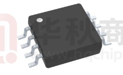
封装
VSSOP (8)
封装尺寸(标称值)
3.00mm × 3.00mm
(1) 如需了解所有可用封装,请参阅数据表末尾的可订购产品附
录。
服务器
路由器(路由设备)
工业设备
个人计算机
功耗敏感型 应用
器件比较
3 说明
2
TCA9802 是一款适用于 I C 总线和 SMBus/PMBus 系
统的双通道双向缓冲器。它在低电压(低至 0.8V)和
较高电压(1.65V 至 3.6V)之间提供双向电平转换。
TCA9802 在器件 B 侧 具有 一个内部电流源,因而 B
侧不需要外部上拉电阻器。该电流源还提供改进的上升
时间和超低功耗。
器件型号
ICS:电流源值(典型
值)
TCA9800
0.54mA
TCA9801
1.1mA
TCA9802
2.2mA
TCA9803
3.3mA
简化原理图
I2C or SMBus Master
(e.g. Processor)
1
8
VCCA
VCCB
3
SDAA
SDAB
2
SCLA
5
EN
6
I2C Slave Devices
TCA9802
SCLB
7
GND
4
Copyright © 2017, Texas Instruments Incorporated
1
本文档旨在为方便起见,提供有关 TI 产品中文版本的信息,以确认产品的概要。 有关适用的官方英文版本的最新信息,请访问 www.ti.com,其内容始终优先。 TI 不保证翻译的准确
性和有效性。 在实际设计之前,请务必参考最新版本的英文版本。
English Data Sheet: SCPS266
�TCA9802
ZHCSG41B – MARCH 2017 – REVISED FEBRUARY 2020
www.ti.com.cn
目录
1
2
3
4
5
6
7
8
9
特性 ..........................................................................
应用 ..........................................................................
说明 ..........................................................................
修订历史记录 ...........................................................
Device Comparison Table.....................................
Pin Configuration and Functions .........................
Specifications.........................................................
1
1
1
2
3
3
4
7.1
7.2
7.3
7.4
7.5
7.6
7.7
7.8
4
4
4
4
5
6
6
7
Absolute Maximum Ratings ......................................
ESD Ratings..............................................................
Recommended Operating Conditions.......................
Thermal Information ..................................................
Electrical Characteristics...........................................
Timing Requirements ................................................
Switching Characteristics ..........................................
Typical Characteristics ..............................................
Parameter Measurement Information .................. 9
Detailed Description ............................................ 10
9.1 Overview ................................................................. 10
9.2 Functional Block Diagram ....................................... 11
9.3 Feature Description................................................. 12
9.4 Device Functional Modes........................................ 13
10 Application and Implementation........................ 16
10.1 Application Information.......................................... 16
10.2 Typical Application ................................................ 18
11 Power Supply Recommendations ..................... 29
12 Layout................................................................... 30
12.1 Layout Guidelines ................................................. 30
12.2 Layout Example .................................................... 30
13 器件和文档支持 ..................................................... 31
13.1
13.2
13.3
13.4
13.5
13.6
文档支持................................................................
接收文档更新通知 .................................................
支持资源................................................................
商标 .......................................................................
静电放电警告.........................................................
Glossary ................................................................
31
31
31
31
31
31
14 机械、封装和可订购信息 ....................................... 31
4 修订历史记录
Changes from Revision A (March 2017) to Revision B
•
Page
Added last sentence: "When enable is a logic LOW while VCCB is powered on, the internal current source on B
side is still enabled...." to the Active-High Repeater Enable Input section........................................................................... 12
Changes from Original (March 2017) to Revision A
Page
•
Updated ICS typical values in Device Comparison Table........................................................................................................ 3
2
Copyright © 2017–2020, Texas Instruments Incorporated
�TCA9802
www.ti.com.cn
ZHCSG41B – MARCH 2017 – REVISED FEBRUARY 2020
5 Device Comparison Table
Part Number
ICS: Current Source Value (Typical)
TCA9800
0.54 mA
TCA9801
1.1 mA
TCA9802
2.2 mA
TCA9803
3.3 mA
6 Pin Configuration and Functions
DGK Package
8-Pin VSSOP
Top View
VCCA
1
8
VCCB
SCLA
2
7
SCLB
SDAA
3
6
SDAB
GND
4
5
EN
Not to scale
Pin Functions
PIN
TYPE
DESCRIPTION
NO.
NAME
1
VCCA
Supply
2
SCLA
I/O
Serial clock bus, A-side. Connect to VCCA through a pull-up resistor, even if unused
3
SDAA
I/O
Serial data bus, A-side. Connect to VCCA through a pull-up resistor, even if unused
4
GND
—
Ground
5
EN
I
6
SDAB
I/O
Serial data bus, B-side. Do NOT connect to VCCB through a pull-up resistor for proper operation. If
unused, leave floating
7
SCLB
I/O
Serial clock bus, B-side. Do NOT connect to VCCB through a pull-up resistor for proper operation. If
unused, leave floating
8
VCCB
Supply
A-side supply voltage (0.8 V to 3.6 V)
Active-high repeater enable input, referenced to VCCA
B-side and device supply voltage (1.65 V to 3.6 V)
Copyright © 2017–2020, Texas Instruments Incorporated
3
�TCA9802
ZHCSG41B – MARCH 2017 – REVISED FEBRUARY 2020
www.ti.com.cn
7 Specifications
7.1 Absolute Maximum Ratings
over operating free-air temperature range (unless otherwise noted) (1)
MIN
MAX
UNIT
VCCA
Supply voltage on A-side
–0.5
4
V
VCCB
Supply voltage on B-side
–0.5
4
V
VEN
Enable input voltage
–0.5
4
V
VI/O
I2C bus voltage
–0.5
4
V
IOL
Maximum SDAA, SCLA IOL current
20
mA
Input clamp current (SDAB/SCLB)
–20
mA
Input clamp current (EN, VCCA, VCCB, SDAA, SCLA)
–20
mA
Output clamp current (SDAB/SCLB)
–20
mA
Output clamp current (EN, VCCA, VCCB, SDAA, SCLA)
–20
mA
Operating junction
temperature
TJ
130
°C
Storage temperature
Tstg
150
°C
IIK
IOK
(1)
–60
Stresses beyond those listed under Absolute Maximum Ratings may cause permanent damage to the device. These are stress ratings
only and functional operation of the device at these or any other conditions beyond those indicated under Recommended Operating
Conditions is not implied. Exposure to absolute-maximum-rated conditions for extended periods may affect device reliability.
7.2 ESD Ratings
VALUE
V(ESD)
(1)
(2)
Electrostatic discharge
Human body model (HBM), per ANSI/ESDA/JEDEC JS001, all pins (1)
±2000
Charged device model (CDM), per JEDEC specification
JESD22-C101, all pins (2)
±1000
UNIT
V
JEDEC document JEP155 states that 500-V HBM allows safe manufacturing with a standard ESD control process.
JEDEC document JEP157 states that 250-V CDM allows safe manufacturing with a standard ESD control process.
7.3 Recommended Operating Conditions
over operating free-air temperature range (unless otherwise noted)
MIN
MAX
UNIT
TA
Operating free-air temperature
–40
125
°C
VCCA
Supply voltage
0.8
3.6
V
VCCB
Supply voltage
1.65
3.6
V
SDAA, SCLA
0
3.6
VI/O
Input-output voltage
SDAB, SCLB
0
3.6
EN
0
3.6
V
7.4 Thermal Information
TCA9802
THERMAL METRIC
(1)
DGK (VSSOP)
UNIT
8 PINS
RθJA
Junction-to-ambient thermal resistance
RθJC(top)
Junction-to-case (top) thermal resistance
RθJB
Junction-to-board thermal resistance
ΨJT
Junction-to-top characterization parameter
18.3
°C/W
ΨJB
Junction-to-board characterization parameter
102.8
°C/W
(1)
4
174.1
°C/W
85
°C/W
104.4
°C/W
For more information about traditional and new thermal metrics, see the Semiconductor and IC Package Thermal Metrics application
report.
Copyright © 2017–2020, Texas Instruments Incorporated
�TCA9802
www.ti.com.cn
ZHCSG41B – MARCH 2017 – REVISED FEBRUARY 2020
7.5 Electrical Characteristics
over operating free-air temperature range (unless otherwise noted)
PARAMETER
TEST CONDITIONS
MIN TYP (1)
MAX
UNIT
OUTPUT CHARACTERISTICS
VOL
Low-level output voltage
IEXT-I
(2)
IEXT-O
ICS
(2)
SDAA, SCLA
IOL = 6 mA, VILB = 0 V
0.04
0.13
SDAB, SCLB
VIA = 0 V
0.22
0.26
Allowed input leakage current of ICS
SDAB, SCLB
0
Allowed output leakage current of ICS
SDAB, SCLB
0
Current source value
200
200
2.2
Current source tolerance
–25
V
µA
µA
mA
25
%
450
kΩ
INPUT CHARACTERISTICS
REN
Enable pin pull-up
VIH
150
High-level input voltage
SDAA, SCLA
VCCA
SDAB, SCLB (3)
0.7 ×
VCCB
VCCB
EN
0.7 ×
VCCA
VCCA
0
0.3 ×
VCCA
0
0.3 ×
VCCB
0
0.3 ×
VCCA
SDAA, SCLA
VIL
SDAB, SCLB (4)
Low-level input voltage
250
0.7 ×
VCCA
(3)
EN
IILC
Low-level input current contention
SDAB, SCLB (4)
RILC
Low-level allowed pull-down resistance
SDAB, SCLB (3)
CBUS
Bus capacitance limit
SDAB, SCLB (5)
800
V
V
µA
0
150
Ω
400
pF
DC CHARACTERISTICS
VCCA
UVLO
Under-voltage lock out
VCCB
ICCA
ICCB
(1)
(2)
(3)
(4)
(5)
Quiescent supply current for VCCA
Quiescent supply current for VCCB
VCCA rising and falling; VCCB =
1.65 or 3.6 V
0.3
0.55
0.8
VCCB rising; VCCA = 0.8 or 3.6 V
1.3
1.51
1.6
VCCB falling; VCCA = 0.8 or 3.6 V
1.2
1.4
1.6
SDAA = SCLA = VCCA = 0.8 V
VCCA or
VCCA = 1.8 V
GND, SDAB =
VCCA = 2.5 V
SCLB = open,
EN = VCCA
VCCA = 3.6 V
0.1
7
0.1
8
0.2
9
0.2
12
Both channels
high, SDAA =
SCLA = pulled
up to
VCCA, SDAB =
SCLB = open,
EN = VCCA
VCCB = 1.8 V
33
60
VCCB = 2.5 V
36
65
VCCB = 3.6 V
41
75
Both channels
VCCB = 1.8 V
low, SDAA =
VCCB = 2.5 V
SCLA = GND.
SDAB = SCLB =
VCCB = 3.6 V
open, EN =
VCCA
4.3
5.2
4.4
5.2
V
µA
µA
mA
4.5
5.3
All typical values are at nominal supply voltage (1.8 V) and TA = 25 °C unless otherwise specified.
SDAB, SCLB may not sink current from external sources. It is required that no source of external current be used on these pins for
proper device operation due to the internal current source.
Parameter specified by design. Not tested in production.
VIL specification is for the first low-level seen by the SDAB and SCLB pins. IILC must also be satisfied in order to be interpreted as a low.
SDAB, SCLB have a maximum supported capacitive load for device operation. If this load capacitance maximum is violated, the device
does not function properly. SDAA, SCLA have no maximum capacitance limit.
Copyright © 2017–2020, Texas Instruments Incorporated
5
�TCA9802
ZHCSG41B – MARCH 2017 – REVISED FEBRUARY 2020
www.ti.com.cn
Electrical Characteristics (continued)
over operating free-air temperature range (unless otherwise noted)
PARAMETER
VCCA = VCCB = 1.8 V,
SDAA/SCLA = VCCA,
SDAB/SCLB = VCCB
ICCA + ICCB Total quiescent supply current
II
Input leakage current
CIO
I/O Capacitance
MIN TYP (1)
TEST CONDITIONS
SDAA, SCLA
MAX
UNIT
34
µA
VI = VCCA, EN = GND
±10
VI = GND, EN = GND
±10
SDAB, SCLB
VCCB = 0 V, VI = 3.6 V
±10
SDAA, SCLA
VI = 0 V or 3.3 V, f = 1 MHz
2
SDAB, SCLB
VCCB = GND, VI = 0 V, f = 1 MHz
8
µA
10
pF
7.6 Timing Requirements
PARAMETER
fSCL(MAX)
tr
tf
(1)
Rise time
(1)
Fall time
tPHL
(1)
tPLH
(1)
(1)
MIN
TYP
MAX
Port A
57
70
Port B; VCCB = 1.65 V
16
35
Port B; VCCB = 2.5 V
25
50
Port B; VCCB = 3.6 V
Max SCL clock frequency
Propagation delay high-to-low
Propagation delay low-to-high
400
UNIT
kHz
36
75
Port A
9
30
Port B
35
70
Port A to Port B
75
200
Port B to Port A
85
250
Port A to Port B
20
90
Port B to Port A
110
260
ns
ns
ns
ns
Times are specified with loads of 1.35 kΩ and 50 pF on A-side and 50 pF on B-side. Different load resistance and capacitance alter the
rise and fall times, thereby changing the propagation delay.
7.7 Switching Characteristics
over operating free-air temperature range (unless otherwise noted)
TYP
MAX
UNIT
tstartup
Startup time
PARAMETER
65
350
µs
ten
Enable time
280
1000
ns
tdis
Disable time
700
1800
ns
6
MIN
Copyright © 2017–2020, Texas Instruments Incorporated
�TCA9802
www.ti.com.cn
ZHCSG41B – MARCH 2017 – REVISED FEBRUARY 2020
7.8 Typical Characteristics
2.1
60
1.8 V
2.5 V
3.3 V
VOL - Output Low Voltage (mV)
ICS - Current Source (mA)
55
2.05
2
1.95
1.8 V
2.5 V
3.3 V
1.9
-40
-25
-10
5
20 35 50 65 80
TA - Ambient Temperature (°C)
95
50
45
IOLA = 6 mA
40
35
30
25
20
15
10
-40
110 125
Figure 1. Current Source vs Ambient Temperature for
Different VCCB
5
20 35 50 65 80
TA - Ambient Temperature (°C)
95
110 125
D002
150
-40qC
25qC
85qC
125qC
180
150
120
VOL - Output Low Voltage (mV)
VOL - Output Low Voltage (mV)
-10
Figure 2. A-Side Output Low Voltage vs Ambient
Temperature for Different VCCB (IOLA = 6 mA)
210
VCCB = 1.65 V
90
60
30
0
-40qC
25qC
85qC
125qC
125
100
VCCB = 2.5 V
75
50
25
0
0
2
4
6
8
10
12
14
IOLA - Low Level Current (mA)
16
18
20
0
2
4
D003
Figure 3. A-Side Output Low Voltage vs Low Level Current
for Different TA (VCCB = 1.65 V)
6
8
10
12
14
IOLA - Low Level Current (mA)
16
18
20
D004
Figure 4. A-Side Output Low Voltage vs Low Level Current
for Different TA (VCCB = 2.5 V)
120
3
-40qC
25qC
85qC
125qC
105
90
ICCA - Operating Current A-Side (µA)
VOL - Ouput Low Voltage (mV)
-25
D001
75
60
45
30
15
0
0
2
4
6
8
10
12
14
IOLA - Low Level Current (mA)
16
18
20
D005
Figure 5. A-Side Output Low Voltage vs Low Level Current
for Different TA (VCCB = 3.6 V)
Copyright © 2017–2020, Texas Instruments Incorporated
2.5
0.8 V
1.8 V
2.5 V
3.6 V
2
1.5
1
0.5
0
-40
-25
-10
5
20 35 50 65 80
TA - Ambient Temperature (°C)
95
110 125
D006
Figure 6. Operating Current A-Side vs Ambient Temperature
for Different VCCA (A-Side = VCCA & GND)
7
�TCA9802
ZHCSG41B – MARCH 2017 – REVISED FEBRUARY 2020
www.ti.com.cn
Typical Characteristics (continued)
5
40
1.8 V
2.5 V
3.3 V
ICCB - Operating Current B-Side (mA)
ICCB - Operating Current B-Side (µA)
45
SDAB = VCCB
35 SCLB = VCCB
30
25
20
-40
-25
-10
5
20 35 50 65 80
TA - Ambient Temperature (°C)
95
110 125
D007
Figure 7. Operating Current B-Side vs Ambient Temperature
for Different VCCB (B-Side = VCCB)
8
1.8 V
2.5 V
3.3 V
4.75
SDAB = GND
SCLB = GND
4.5
4.25
4
-40
-25
-10
5
20 35 50 65 80
TA - Ambient Temperature (°C)
95
110 125
D008
Figure 8. Operating Current B-Side vs Ambient Temperature
for Different VCCB (B-Side = GND)
Copyright © 2017–2020, Texas Instruments Incorporated
�TCA9802
www.ti.com.cn
ZHCSG41B – MARCH 2017 – REVISED FEBRUARY 2020
8 Parameter Measurement Information
External
pull-down
(A-side)
Off
On
A Side
External
pull-down
(B-side)
Off
tf:B
On
B Side
tr:A
Off
tr:B
tf:B
tPLH:AB
0.7 VCCB
0.7 VCCA
0.7 VCCA
Off
0.3 VCCB
VOL (1)
0.7 VCCB
VOL (3)
VOL (2)
0.3 VCCB
0.3 VCCA
0.3 VCCA
tPHL:BA
tPHL:AB
tf:A
B Side
tr:B
0.7 VCCB
0.3 VCCB
tPLH:BA
0.7 VCCA
tPLH:AB
0.7 VCCB
tr:A
tf:A
A Side
0.3 VCCA
0.7 VCCA
0.3 VCCA
0.3 VCCB
1) The VOL of only the external device, pulling down on the bus
2) The VOL of both the external device and the TCA980x translator
3) The VOL of only the TCA980x, after the external device releases
Figure 9. Propagation Delay and Transition Times
for A-Side to B-Side
VCCB
Figure 10. Propagation Delay for B-Side to A-Side
0.7 VCC B
SDAB
SCLB
UVLOB
(Max)
0.3 VCC B
tstartup
0.9 VCC A
SDAA
SCLA
EN
0.5 VCC A
0.5 VCC A
1) VCCA is powered, SDAA/SCLA are connected to GND
1) VCCA is powered, SDAB/SCLB are connected to GND
Figure 11. Startup Time (tstartup)
Copyright © 2017–2020, Texas Instruments Incorporated
Figure 12. Enable and Disable Time (ten and tdis)
9
�TCA9802
ZHCSG41B – MARCH 2017 – REVISED FEBRUARY 2020
www.ti.com.cn
9 Detailed Description
9.1 Overview
The TCA9802 is a dual-channel bidirectional buffer intended for I2C bus and SMBus/PMBus systems. It provides
bidirectional level shifting (up-translation and down-translation) between low voltages (down to 0.8 V) and higher
voltages (1.65 V to 3.6 V). The TCA9802 features an internal current source on the B-side of the device, allowing
the removal of external pull-up resistors on the B-side. The current source also provides an improved rise time
and ultra-low power consumption.
The TCA9802 is able to provide true buffering (rather than a pass-FET solution) without using a static voltage
offset or incremental offset. This means that the VOL on both the A and B sides of the TCA9802 are very low
(approximately 0.2 V), helping to eliminate communication issues as a result of fixed VIL thresholds. Another key
feature of the TCA9802 is that there are no power sequencing requirements, or power supply dependencies.
VCCA can be greater than, less than, or equal to VCCB. This gives the system designer flexibility with how the
TCA9802 is used.
The TCA9802 is part of a four device family with varying current source strengths (see the Device Comparison
Table).
10
Copyright © 2017–2020, Texas Instruments Incorporated
�TCA9802
www.ti.com.cn
ZHCSG41B – MARCH 2017 – REVISED FEBRUARY 2020
9.2 Functional Block Diagram
VCCA
VCCB
1
8
VCCB
ICS
3
6
SDAA
SDAB
VCCB
ICS
2
7
SCLA
SCLB
VCCA
REN
5
EN
4
GND
For proper device operation, no external current sources (pull-up resistors) must be used on the SDAB and SCLB
ports
Copyright © 2017–2020, Texas Instruments Incorporated
11
�TCA9802
ZHCSG41B – MARCH 2017 – REVISED FEBRUARY 2020
www.ti.com.cn
9.3 Feature Description
9.3.1 Integrated Current Source
The TCA980x family has an integrated current source on the B side. By using an integrated current source, the
device is able to measure current to determine if an external device is pulling down on the bus or not. This
innovative detection method removes the need for a static voltage offset on the B side.
9.3.2 Ultra-Low Power Consumption
The TCA980x family features ultra low power consumption, to help maximum battery life, or cut down on power
dissipation in sensitive applications.
9.3.3 No Static-Voltage Offset
The TCA980x family has no static-voltage offset, which are commonly used in buffered translators to prevent a
device lock-up situation where the buffer's own output low could trip the input low threshold. The removal of the
static voltage offset is significant because it allows the device to have low a low VOL on the B side, which helps
prevents communication issues that arise from connecting a static-voltage offset output device to an input with
an input low threshold which is below the static voltage VOL.
9.3.4 Active-High Repeater Enable Input
The TCA980x has an active-high enable (EN) input with an internal pull-up to VCCA, which allows the user to
select when the repeater is active. This can be used to isolate a badly behaved slave on power-up reset. The EN
input must change state only when the global bus and repeater port are in an idle state. to prevent system or
communication failures. When enable is a logic LOW while VCCB is powered on, the internal current source on
B side is still enabled. The enable pin does not disable the internal current source.
9.3.5 Powered Off High Impedance I2C Bus Pins on A-Side
The SCLA and SDAA pins enters a high impedance state when either VCCA or VCCB fall below their UVLO
voltages. These pins are safe to continue having I2C communication on, even when the device is disabled or has
no power.
The SCLB and SDAB pins remain powered by their current source (ICS), even when VCCA is below UVLO.
When VCCB falls below UVLO, the current source turns off, and a weak pull-up is connected to prevent the Bpins from floating. This is intended behavior, because no external pull-up resistors are to be used on the SDAB
or SCLB pins. This behavior prevents the bus pins from floating, and allows it to follow VCCB.
9.3.6 Powered-Off Back-Power Protection for I2C Bus Pins
All I2C bus pins has protection circuitry to prevent current from flowing to the VCC pins from the I2C bus pins.
9.3.7 Clock Stretching and Multiple Master Arbitration Support
The TCA980x family supports clock stretching and multiple master arbitration methods, and helps to minimize
overshoot during these hand offs between master and slave (or multiple masters).
12
Copyright © 2017–2020, Texas Instruments Incorporated
�TCA9802
www.ti.com.cn
ZHCSG41B – MARCH 2017 – REVISED FEBRUARY 2020
9.4 Device Functional Modes
Table 1 shows the TCA980x function table.
Table 1. Enable Function Table
INPUT
EN
FUNCTION
L
Outputs disabled
H
SDAA = SDAB
SCLA = SCLB
Table 2 lists the TCA980x B-Side current source functions.
Table 2. B-Side Current Source Function Table
VCCB
FUNCTION
L
Current sources disabled, weak pull-up is connected with back-power protection
H
Current sources enabled
9.4.1 Device Operation Considerations
9.4.1.1 B-Side Input Low (VIL/IILC/RILC)
The TCA980x family utilizes the current source on the B side to determine whether an external device is driving
the bus low, or if it is driving the bus low itself. As such, there are some parameters that must be met to ensure a
successful transmission of a low from the B-side to the A-side. These parameters are listed in Table 3.
Table 3. B-side Input Low-Level Parameters
PARAMETER
SHORT DESCRIPTION
VIL
Low-level input voltage
The input voltage that is interpreted as a low. On the B-side, IILC must
also be satisfied to maintain a low
IILC
Low-level input current
(contention)
The minimum amount of current that an external device must be sinking
from the TCA980x to transmit a low. VIL must also be satisfied
RILC
Low-level allowed pulldown resistance
The maximum allowed pull-down resistance of an external device in
order to successful transmit a low
DETAILED INFORMATION
See the VILC & IILC section
See the VILC & IILC section
See the RILC section
9.4.1.1.1 VILC & IILC
The IILC parameter is the minimum amount of current that the external device must sink from the TCA980x in
order for the TCA980x to accept the low on the B-side.
In order for the TCA980x to accept a low on the B-side, both VIL and IILC parameters must be satisfied. In an idle
bus condition (both A and B sides are high), meeting the VIL threshold with an external device pull-down meets
the IILC requirement, since the pull-down has to sink the entire ICS (current source value) current before the
voltage on the pin falls.
In a contention situation (the A-side is being driven low externally, and the B-side is driven low by the TCA980x),
the VIL requirement is already satisfied by the TCA980x alone (Since the output low voltage is less than the VIL
threshold). In order for a device on the B-side to over-drive the A-side, it must sink the IILC value for the TCA980x
to accept that the low is now being driven by the B-side. This helps reduce or eliminate overshoot during the
hand off between a slave an master during a clock-stretching event, or an acknowledge.
External pull-up resistors on the B-side are not allowed for this reason. As the additional current provided by
them may hinder an external device from being able to satisfy the TCA980x's IILC requirement. For more
information on this and allowed external current into the device, see the Input and Output Leakage Current (IEXTI/IEXT-O) section.
Copyright © 2017–2020, Texas Instruments Incorporated
13
�TCA9802
ZHCSG41B – MARCH 2017 – REVISED FEBRUARY 2020
www.ti.com.cn
9.4.1.1.2 RILC
The RILC parameter describes the maximum allowed pull-down resistance. This parameter comes from the
combination of IILC and ICS, and states the maximum resistance that can satisfy the IILC parameter. Note that
series resistors on the bus are going to affect this, as seen with other types of buffers (voltage delta across the
series resistor. This increases the effective VOL of the external device pulling the bus low).
The calculated resistance of the internal pull-down FET of an external device can be calculated from the VOL and
IOL measurements of the external device in question using Equation 1. Take care to consider any series resistors
placed in the path from the TCA980x to any external device. Note that RPD is the calculated resistance of the
internal pull-down FET, and not a resistor to ground. This is for determining if the external device's output
characteristics meet the TCA980x RILC requirement (150 Ω).
RPD
VOL / IOL
(1)
9.4.1.2 Input and Output Leakage Current (IEXT-I/IEXT-O)
The Input external current (IEXT-I) and output external current (IEXT-O) parameters describe the amount of parasitic
current either injected into the device or pulled from the device (such as leakage from ESD cells) without
affecting device operation as shown in Table 4.
Table 4. B-Side Input and Output Leakage Current
PARAMETER
SHORT DESCRIPTION
DETAILED
INFORMATION
IEXT-I
Input leakage current
Current that is external, but pulled up to supply, leaking current into the TCA980x
B-side. An example is a leaky ESD cell from VCC, or an external pull-up resistor.
See the IEXT-I
section
IEXT-O
Output leakage current
Current that is pulled from the TCA980x B-side. ESD cells are the most common
form of output leakage. Care must be taken not to violate this spec, otherwise the
leakage current can create a false low.
See the IEXT-O
section
9.4.1.2.1 IEXT-I
IEXT-I is a current source that is external to the TCA980x B-side, but leaks current into the device. This type of
input leakage may not exceed the IEXT-I maximum spec, or else the minimum IILC value does not apply.
TCA980x
I2C Slave
VCCB
ICS
A-Side
B-Side
Figure 13. IEXT-I Example
As shown in Figure 13, IEXT-I is a source of additional current into the device, shown as a leaky ESD cell. The
user must keep IEXT-I as close to 0 as possible, since the TCA980x has a current source as a pull-up internally,
and uses this current source to help detect which side is driving a low. As IEXT-I increases, it increases the
minimum IILC value, requiring that an external device sink more current from the TCA980x in order to transmit a
low. There must be no external pull-up resistor on the B-side to contribute to IEXT-I.
14
Copyright © 2017–2020, Texas Instruments Incorporated
�TCA9802
www.ti.com.cn
ZHCSG41B – MARCH 2017 – REVISED FEBRUARY 2020
9.4.1.2.2 IEXT-O
IEXT-O is an unintentional current from the TCA980x's internal current source that is external. Leaking ESD cells
are a common contributor to leakage current. This type of input leakage may not exceed the IEXT-O maximum
spec, or else the TCA980x can interpret this excessive current as an external device transmitting a low, causing
the bus to latch. It is important to consider the total sum of I2C slave device's leakage to ground, and that it does
not violate IEXT-O. An example showing a typical IEXT-O leakage path through an ESD cell is shown in Figure 14.
TCA980x
I2C Slave
VCCB
ICS
A-Side
B-Side
Figure 14. IEXT-O Example
Copyright © 2017–2020, Texas Instruments Incorporated
15
�TCA9802
ZHCSG41B – MARCH 2017 – REVISED FEBRUARY 2020
www.ti.com.cn
10 Application and Implementation
NOTE
Information in the following applications sections is not part of the TI component
specification, and TI does not warrant its accuracy or completeness. TI’s customers are
responsible for determining suitability of components for their purposes. Customers should
validate and test their design implementation to confirm system functionality.
10.1 Application Information
10.1.1 Device Selection Guide
The TCA980x family has 4 different variants, with different strengths of the internal current source as shown in
Table 5.
Table 5. TCA980x Family
Part Number
ICS: Current Source Value
TCA9800
0.54 mA
TCA9801
1.1 mA
TCA9802
2.2 mA
TCA9803
3.3 mA
It is acceptable to select the TCA9803 as the default, since it is able to drive 400-pF bus capacitance loads at
400 kHz. For system designers looking to optimize selection, see the Detailed Design Procedure section for
single device for detailed examples of how to select a part number for a specific application.
10.1.2 Special Considerations for the B-side
The TCA980x supports many types of connections between other TCA980x and other buffers/translators. Care
must be taken to ensure that all of the B-side requirements be satisfied. For example, FET/pass-gate based
translators typically cannot be used on the B-side, because they require pull-up resistors on both sides, and
when one side is pulling low, the FET/switch closes, likely causing IEXT-I to be violated (See the IEXT-I section for
more information).
The FET or Pass-Gate Translators and Buffered Translators/Level-shifters sections list some use-cases that are
not supported or require special considerations when connected to the B-ports, note that these considerations
only apply to the B-side of the TCA980x family.
10.1.2.1 FET or Pass-Gate Translators
Some translators are based on pass-gates for translation support. In most of the use cases, external pull-up
resistors are required to pull the bus to the voltage rail.
16
Copyright © 2017–2020, Texas Instruments Incorporated
�TCA9802
www.ti.com.cn
ZHCSG41B – MARCH 2017 – REVISED FEBRUARY 2020
1.65 V
3.3 V
5k
1.65 V
5k
5k
VCCA
VCCB
VCCB
5k
VCCA
TCA980x
SDA
SDAA
SDAB
SCL
SCLA
SCLB
BUS
MASTER
400 kHz
SDA
SCL
FET Based
SLAVE
400 kHz
EN
Copyright © 2017, Texas Instruments Incorporated
Figure 15. Incorrect B-Side Pass-Gate Based Translator Use Case
1.65 V
3.3 V
5k
VCCB
VCCA
1.65 V
5k
5k
VCCB
5k
VCCA
TCA980x
SDA
SDAB
SDAA
SCL
SCLB
SCLA
BUS
MASTER
400 kHz
SDA
SCL
FET Based
SLAVE
400 kHz
EN
Open Drain
Copyright © 2017, Texas Instruments Incorporated
Figure 16. A-Side Pass-Gate Based Translator Use Case
As shown in Figure 15, it may appear that this use case is valid, but actually it is not. When either the TCA980x
B-side or the slave pull down on the bus, the FET isolating the bus closes (low RDS_ON) and current from the 5kΩ resistor is observed by the TCA980x, violating IEXT-I. See the IEXT-I section for more information.
Figure 16 shows the correct way to pair with a FET base translator (connecting to the A-side).
Rather than using a FET-based translator, it is recommended that a buffered translator be used, such as another
TCA980x or a TCA9517. See the Typical Application section for single device for more information on concerns
with B-side connections to buffered translators.
10.1.2.2 Buffered Translators/Level-shifters
The TCA980x family supports connections with buffered translators, but care must be taken to ensure that no
operating conditions be violated. In a general sense, the following must be avoided on the B-side ports of the
TCA980x:
• Sources of current other than the individual TCA980x (B-side of the other TCA980x, external pull-up resistors,
current sources, rise time accelerators, etc)
• Static-voltage offset buffer outputs (B-side of the TCA9517, etc)
• Outputs with RILC (equivalent pull-down resistance) > 150 Ω
Copyright © 2017–2020, Texas Instruments Incorporated
17
�TCA9802
ZHCSG41B – MARCH 2017 – REVISED FEBRUARY 2020
www.ti.com.cn
It is important to note that these special operating requirements apply only to the B-side ports of the TCA980x.
For example, the TCA9517 B-side can be safely connected to the A-side of the TCA980x, but not to the B-side of
the TCA980x. However, it is OK to connect the A-side of the TCA9517 to the B-side (or A-side) of the TCA980x,
because the A-side does not have a static voltage offset based output.
Figure 17 shows an example of the incorrect connection on the B-side to a buffer with a static voltage offset
output. The reason this is unacceptable is because the equivalent output resistance of the output buffer is
greater than the maximum RILC allowed. See the RILC section for more information.
1.65 V
5k
3.3 V
1.65 V
5k
5k
VCCA
VCCB
VCCB
TCA980x
5k
VCCA
T/PCA9517
SDA
SDAA
SDAB
SDAB
SDAA
SDA
SCL
SCLA
SCLB
SCLB
SCLA
SCL
BUS
MASTER
400 kHz
SLAVE
400 kHz
EN
Copyright © 2017, Texas Instruments Incorporated
Figure 17. Incorrect B-Side Static Voltage Offset Buffer Connection
1.65 V
5k
3.3 V
5V
5k
5k
VCCA
VCCB
TCA980x
VCCA
5k
VCCB
T/PCA9517
SDA
SDAA
SDAB
SDAA
SDAB
SDA
SCL
SCLA
SCLB
SCLA
SCLB
SCL
BUS
MASTER
400 kHz
SLAVE
400 kHz
EN
Copyright © 2017, Texas Instruments Incorporated
Figure 18. Correct Connection With Other Buffers
NOTE
Decoupling capacitors are not shown to keep the illustration simple. Decoupling capacitors
(1 µF and 0.1 µF) must be placed close to each power supply pin.
As shown in Figure 18, this connection is acceptable for use on the B-side ports of the TCA980x, because the
equivalent RILC of the A-side of this example buffer is less than 150 Ω.
10.2 Typical Application
10.2.1 Single Device
The typical application for the TCA980x family is to be used as a buffering translator, where the VCCA and VCCB
are at different values in order to level-shift the I2C bus voltages.
18
Copyright © 2017–2020, Texas Instruments Incorporated
�TCA9802
www.ti.com.cn
ZHCSG41B – MARCH 2017 – REVISED FEBRUARY 2020
Typical Application (continued)
It is critical to note that there are no external sources of current allowed on the B-side ports, since this can affect
device operation as shown in the IEXT-I section.
1.2 V
5k
3.3 V
5k
VCCA VCCB
TCA980x
BUS
MASTER
400 kHz
SDA
SDAA SDAB
SDA
SCL
SCLA SCLB
SCL
SLAVE
400 kHz
EN
Copyright © 2017, Texas Instruments Incorporated
Figure 19. Typical Level-Shifting Application Example (Master on A-side)
NOTE
Decoupling capacitors are not shown to keep the illustration simple. Decoupling capacitors
(1 µF and 0.1 µF) must be placed close to each power supply pin.
As shown in Figure 20, the I2C master can be on the B-side, and that it is ok to have VCCA > VCCB. The only
requirements are that no external source of current (pull-up resistor or current source) be on the B-pins of the
TCA980x, and that both VCCA/VCCB values are within the recommended range. As a note, since the EN pin is
referenced to the VCCA supply voltage, when the master is on the A-side, the system designer must ensure that
the enable pin voltage is pulled up to VCCA (either with an external or the internal pull-up resistor) to ensure that
the device is enabled.
1.65 V
3.3 V
5k
5k
VCCB VCCA
TCA980x
BUS
MASTER
400 kHz
SDA
SDAB SDAA
SDA
SCL
SCLB SCLA
SCL
EN
SLAVE
400 kHz
Copyright © 2017, Texas Instruments Incorporated
Figure 20. Typical Level-Shifting Application Example (Master on B-side)
NOTE
Decoupling capacitors are not shown to keep the illustration simple. Decoupling capacitors
(1 µF and 0.1 µF) must be placed close to each power supply pin.
Copyright © 2017–2020, Texas Instruments Incorporated
19
�TCA9802
ZHCSG41B – MARCH 2017 – REVISED FEBRUARY 2020
www.ti.com.cn
Typical Application (continued)
10.2.1.1 Design Requirements
The system designer must first select the correct variant of the TCA980x family for the load. In order to do this,
the information in Table 6 must be known. The setup in Figure 19 is used for these example design
requirements.
CL is the capacitance of the bus, including the pin capacitance of each slave device connected, and the
capacitance of the board trace. It is possible to estimate the bus capacitance by summing up the pin
capacitances of each slave device on the node (using 10-pF per slave is a safe estimate, since this is the
maximum allowed per the I2C specification), but trace capacitance requires an estimation through simulation or
by getting the capacitance per unit length from the board manufacturer.
Table 6. Design Requirements
Parameter
Description
Acceptable Range
Example Value/Target
CL
Load capacitance (bus capacitance) on Bside
up to 400 pF
100 pF
tr
Rise time
up to 300 ns
≤ 150 ns
VCCA
VCCA supply voltage
0.8 V-3.6 V
1.2 V
VCCB
VCCB supply voltage
1.65 V-3.6 V
fSCL
I2C clock frequency
3.3 V
400 kHz
10.2.1.2 Detailed Design Procedure
Selection of the correct device is important for designers wanting optimize power consumption while transmitting.
Selecting the pull-up resistor required for the A-side is well documented already, see the I2C Bus Pullup Resistor
Calculation application report. The rest of this section deals only with selection of a device based on the B-side
design requirements.
Since the B-ports of the TCA980x family have an integrated current source, the rise time is easily calculated with
Equation 2. The graphs in the Application Curves section show the maximum capacitance load that each device
can drive (based on minimum ICS value) to achieve a desired rise time, for different VCCB voltages.
tr
CL
(0.4 u VCCB )
I CS
(2)
The target design requirements example is intended for 400-kHz I2C, so the appropriate selection graph to use is
Figure 22, and specifically Figure 27 since VCCB supply voltage is 3.3 V. In Figure 21, the graph has the
appropriate regions shaded to help illustrate how to select the appropriate device. When looking at the general
selection graphs, note that voltage line shifts evenly between the 1.65 V and 3.6 V traces in the general selection
graphs. For example, if VCCB in another example is 2.5 V, then the selection graph is based on a line in the
middle of the 1.65 V and the 3.6 V trace.
As shown in Figure 21, the shaded region is the appropriate region based on design requirements listed in
Table 6. Any line that touches this shaded region is able to meet the design requirements. In this example, the
TCA9803 and the TCA9802 both are able to satisfy the design requirements, since they both touch the shaded
region. The TCA9800 and the TCA9801 both fall below the shaded region. While the TCA9801 is able to meet a
rise time of about 190 ns at 100 pF (acceptable by the fast-mode rise time requirements), the design target in
this example was ≤ 150 ns. This is a consideration a system designer can make, sacrificing rise time for a lowerpower device, but in this example, the 150 ns limit is going to be upheld).
20
Copyright © 2017–2020, Texas Instruments Incorporated
�TCA9802
www.ti.com.cn
ZHCSG41B – MARCH 2017 – REVISED FEBRUARY 2020
Max Capacitance Load (pF)
400
TCA9800
TCA9801
TCA9802
TCA9803
300
VCCB = 3.3 V
200
100
0
0
50
100
150
200
tr - Rise Time (ns)
250
300
D001
Figure 21. Selection Guide Based on Example Design Requirements
NOTE
Decoupling capacitors are not shown to keep the illustration simple. Decoupling capacitors
(1 µF and 0.1 µF) must be placed close to each power supply pin.
Based on the selection graph shown above, the TCA9802 is selected, since it is the lowest-power device's trace
(grey trace) which touches the shaded region. The TCA9803 may also be used without any consequences.
Copyright © 2017–2020, Texas Instruments Incorporated
21
�TCA9802
ZHCSG41B – MARCH 2017 – REVISED FEBRUARY 2020
www.ti.com.cn
10.2.1.3 Application Curves
The application curves can be used to select the appropriate part for a given design requirement, or to estimate
the rise-time.
400
400
TCA9803 (1.65 V)
300
TCA9801 (1.65 V)
200
TCA9803 (3.6 V)
TCA9802 (1.65 V)
TCA9800 (1.65 V)
TCA9802 (3.6 V)
100
Max Capacitance (pF)
Max Capacitance (pF)
TCA9803 (1.65 V)
300
TCA9801 (1.65 V)
200
TCA9802 (1.65 V)
TCA9800 (1.65 V)
TCA9802 (3.6 V)
100
TCA9801 (3.6 V)
0
30
60
90
120 150 180 210
tr - Rise Time (ns)
270
300
0
60
90
120 150 180 210
tr - Rise Time (ns)
240
270
300
D001
Figure 22. Maximum Load Capacitance vs Rise Time (400kHz I2C)
Figure 23. Maximum Load Capacitance vs Rise Time (100kHz I2C)
400
400
TCA9800
TCA9801
TCA9802
TCA9803
300
VCCB = 1.65 V
200
100
TCA9800
TCA9801
TCA9802
TCA9803
300
VCCB = 1.8 V
200
100
0
0
50
100
150
200
tr - Rise Time (ns)
250
300
0
50
D001
100
150
200
tr - Rise Time (ns)
250
300
D001
Figure 24. Maximum Load Capacitance vs Rise Time (400kHz I2C, VCCB = 1.65 V)
Figure 25. Maximum Load Capacitance vs Rise Time (400kHz I2C, VCCB = 1.8 V)
400
400
TCA9800
TCA9801
TCA9802
TCA9803
300
Max Capacitance Load (pF)
Max Capacitance Load (pF)
30
D001
0
VCCB = 2.5 V
200
100
0
TCA9800
TCA9801
TCA9802
TCA9803
300
VCCB = 3.3 V
200
100
0
0
50
100
150
200
tr - Rise Time (ns)
250
300
D001
Figure 26. Maximum Load Capacitance vs Rise Time (400kHz I2C, VCCB = 2.5 V)
22
TCA9800 (3.6 V)
0
240
Max Capacitance Load (pF)
Max Capacitance Load (pF)
TCA9801 (3.6 V)
TCA9800 (3.6 V)
0
TCA9803 (3.6 V)
0
50
100
150
200
tr - Rise Time (ns)
250
300
D001
Figure 27. Maximum Load Capacitance vs Rise Time (400kHz I2C, VCCB = 3.3 V)
Copyright © 2017–2020, Texas Instruments Incorporated
�TCA9802
www.ti.com.cn
ZHCSG41B – MARCH 2017 – REVISED FEBRUARY 2020
Max Capacitance Load (pF)
400
TCA9800
TCA9801
TCA9802
TCA9803
300
VCCB = 3.6 V
200
100
0
0
50
100
150
200
tr - Rise Time (ns)
250
300
D001
Figure 28. Maximum Load Capacitance vs Rise Time (400-kHz I2C, VCCB = 3.6 V)
10.2.2 Buffering Without Level-Shifting
The TCA980x family supports buffering use cases which do not need level-shifting or voltage-translation.
It is critical to note that there are no external sources of current allowed on the B-side ports, since this can affect
device operation as shown in the IEXT-I section.
2.5 V
5k
5k
VCCA VCCB
TCA980x
BUS
MASTER
400 kHz
SDA
SDAA SDAB
SDA
SCL
SCLA SCLB
SCL
SLAVE
400 kHz
EN
Copyright © 2017, Texas Instruments Incorporated
Figure 29. Buffering Use Case Without Level-Shifting
NOTE
Decoupling capacitors are not shown to keep the illustration simple. Decoupling capacitors
(1 µF and 0.1 µF) must be placed close to each power supply pin.
10.2.2.1 Design Requirements
The system designer must first select the correct variant of the TCA980x family for the load. In order to do this,
the information in Table 7 must be known. The setup in Figure 29 is used for these example design
requirements.
Table 7. Design Requirements
Parameter
Description
Acceptable Range
Example Value/Target
CL
Load capacitance (bus capacitance) on Bside
up to 400 pF
200 pF
tr
Rise time
up to 300 ns
≤ 300 ns
Copyright © 2017–2020, Texas Instruments Incorporated
23
�TCA9802
ZHCSG41B – MARCH 2017 – REVISED FEBRUARY 2020
www.ti.com.cn
Table 7. Design Requirements (continued)
Parameter
Description
Acceptable Range
Example Value/Target
VCCA
VCCA supply voltage
0.8 V-3.6 V
2.5 V
VCCB
VCCB supply voltage
1.65 V-3.6 V
fSCL
I2C clock frequency
2.5 V
400 kHz
10.2.2.2 Detailed Design Procedure
Selecting the pull-up resistor required for the A-side is well documented already, see the I2C Bus Pullup Resistor
Calculation application report. The rest of this section deals only with selection of a device based on the B-side
design requirements.
Selection process of each device is identical to the procedure described in the Device Selection Guide section,
except that it must be done for each individual TCA980x. This section jumps straight to the selection graphs to
show the selection process. See the Detailed Design Procedure section for single device for detailed information.
As shown in Figure 30, the shaded region is the appropriate region based on design requirements listed in
Table 7. Any line that touches this shaded region is able to meet the design requirements. In this example, the
TCA9803, TCA9802, and TCA9801 are able to satisfy the design requirements, since they all touch the shaded
region. The TCA9800 falls below the shaded region.
Based on the selection graph shown above, the TCA9801 is selected, since it is the lowest-power device which
touches the shaded region (red trace). The TCA9803 or the TCA9802 may also be used without any
consequences.
10.2.2.3 Application Curve
Max Capacitance Load (pF)
400
TCA9800
TCA9801
TCA9802
TCA9803
300
VCCB = 2.5 V
200
100
0
0
50
100
150
200
tr - Rise Time (ns)
250
300
D001
Figure 30. Selection Guide Based On Example Design Requirements
10.2.3 Parallel Device Use Case
The TCA980x family supports multiple TCA980x used in parallel. The A-sides of the TCA980x are allowed to be
connected together.
It is critical to note that there are no external sources of current allowed on the B-side ports, since this can affect
device operation shown in the IEXT-I section.
NOTE: B-sides of TCA980x devices may never be connected to each other, because the IEXT-I specification limit
is violated. See the IEXT-I section for more information.
NOTE: The B-side may not be connected to another translator if it uses a static-voltage offset. The RILC spec is
violated since the static voltage offset adjusts the output resistance to ground to be outside of the RILC spec
requirement, causing the TCA980x to be unable to recognize a low.
24
Copyright © 2017–2020, Texas Instruments Incorporated
�TCA9802
www.ti.com.cn
ZHCSG41B – MARCH 2017 – REVISED FEBRUARY 2020
1.65 V
5k
3.3 V
5k
VCCA VCCB
TCA980x
BUS
MASTER
400 kHz
SDA
SDAA SDAB
SDA
SCL
SCLA SCLB
SCL
SLAVE
400 kHz
EN
1.65 V
BUS B
VCCA VCCB
TCA980x
SDAA SDAB
SDA
SCLA SCLB
SCL
SLAVE
400 kHz
EN
BUS A
BUS C
Copyright © 2017, Texas Instruments Incorporated
Figure 31. Parallel Use Case
NOTE
Decoupling capacitors are not shown to keep the illustration simple. Decoupling capacitors
(1 µF and 0.1 µF) must be placed close to each power supply pin.
10.2.3.1 Design Requirements
The system designer must first select the correct variant of the TCA980x family for the load. In order to do this,
the information shown in Table 8 and Table 9 must be known. The setup in Figure 31 is used for these example
design requirements.
Table 8. Design Requirements for Bus B
Parameter
Description
Acceptable Range
Example Value/Target
CL
Load capacitance (bus capacitance) on Bside
up to 400 pF
300 pF
tr
Rise time
up to 300 ns
≤ 300 ns
VCCA
VCCA supply voltage
0.8 V-3.6 V
1.65 V
VCCB
VCCB supply voltage
1.65 V-3.6 V
3.3 V
Copyright © 2017–2020, Texas Instruments Incorporated
25
�TCA9802
ZHCSG41B – MARCH 2017 – REVISED FEBRUARY 2020
www.ti.com.cn
Table 8. Design Requirements for Bus B (continued)
Parameter
Description
fSCL
I2C clock frequency
Acceptable Range
Example Value/Target
400 kHz
Table 9. Design Requirements for Bus C
Parameter
Description
Acceptable Range
Example Value/Target
CL
Load capacitance (bus capacitance) on Bside
up to 400 pF
40 pF
tr
Rise time
up to 300 ns
≤ 300 ns
VCCA
VCCA supply voltage
0.8 V-3.6 V
1.65 V
VCCB
VCCB supply voltage
1.65 V-3.6 V
fSCL
I2C clock frequency
1.65 V
400 kHz
10.2.3.2 Detailed Design Procedure
Selecting the pull-up resistor required for the A-side (Bus A) is well documented already, see the I2C Bus Pullup
Resistor Calculation application report. The rest of this section deals only with selection of a device based on the
B-side design requirements.
Selection process of each device is identical to the procedure described in the Device Selection Guide section,
except that it must be done for each individual TCA980x. This section jumps straight to the selection graphs to
show the selection process. See the Detailed Design Procedure section for single device for detailed information.
Based on Figure 32, the TCA9802 or the TCA9803 are the devices which are able to meet the design
requirements. The TCA9802 is the most optimized selection, but the TCA9803 can be used without issue.
Based on Figure 33, all 4 variants of the TCA980x family meet the design requirements. The TCA9800 is the
most optimized selection, but any of the variants can be used without issue.
As the system designer, the choice can be made to go for the most optimized part selections (TCA9802 for bus
B and TCA9800 for bus C), but it is also ok to use the TCA9802 or the TCA9803 on both busses, because they
both satisfy the design requirements of both busses.
10.2.3.3 Application Curves
400
TCA9800
TCA9801
TCA9802
TCA9803
300
Max Capacitance Load (pF)
Max Capacitance Load (pF)
400
VCCB = 3.3 V
200
100
0
TCA9800
TCA9801
TCA9802
TCA9803
300
VCCB = 1.65 V
200
100
0
0
50
100
150
200
tr - Rise Time (ns)
250
300
D001
Figure 32. Selection Guide Based On Example Design
Requirements for Bus B
0
50
100
150
200
tr - Rise Time (ns)
250
300
D001
Figure 33. Selection Guide Based On Example Design
Requirements for Bus C
10.2.4 Series Device Use Case
The TCA980x family supports multiple TCA980x used in series. It is acceptable to connect A sides together, or
have A sides connect to B sides, but B-sides may never be connected together.
It is critical to note that there are no external sources of current allowed on the B-side ports, since this can affect
device operation as shown in the IEXT-I section.
26
Copyright © 2017–2020, Texas Instruments Incorporated
�TCA9802
www.ti.com.cn
ZHCSG41B – MARCH 2017 – REVISED FEBRUARY 2020
NOTE: B-sides of TCA980x devices may never be connected to each other, because the IEXT-I specification limit
is violated. See the IEXT-I for more information.
NOTE: The B-side may not be connected to another translator if it uses a static-voltage offset. The RILC spec is
violated since the static voltage offset adjusts the output resistance to ground to be outside of the RILC spec
requirement, causing the TCA980x to be unable to recognize a low.
1.65 V
5k
BUS
MASTER
400 kHz
3.3 V
1.65 V
5k
VCCA VCCB
VCCA VCCB
TCA980x
TCA980x
SDA
SDAA SDAB
SDAA SDAB
SDA
SCL
SCLA SCLB
SCLA SCLB
SCL
EN
EN
BUS A
SLAVE
400 kHz
BUS B
BUS C
Copyright © 2017, Texas Instruments Incorporated
Figure 34. Series Use Case
NOTE
Decoupling capacitors are not shown to keep the illustration simple. Decoupling capacitors
(1 µF and 0.1 µF) must be placed close to each power supply pin.
10.2.4.1 Design Requirements
The system designer must first select the correct variant of the TCA980x family for the load. In order to do this,
the information in Table 10 and Table 11 must be known. The setup in Figure 34 is used for these example
design requirements.
Table 10. Design Requirements for Bus B / 1st TCA980x
Parameter
Description
Acceptable Range
Example Value/Target
CL
Load capacitance (bus capacitance) on Bside
up to 400 pF
300 pF
tr
Rise time
up to 300 ns
≤ 200 ns
VCCA
VCCA supply voltage
0.8 V-3.6 V
1.65 V
VCCB
VCCB supply voltage
1.65 V-3.6 V
3.3 V
fSCL
2
I C clock frequency
400 kHz
Table 11. Design Requirements for Bus C / 2nd TCA980x
Parameter
Description
Acceptable Range
Example Value/Target
CL
Load capacitance (bus capacitance) on Bside
up to 400 pF
100 pF
≤ 250 ns
tr
Rise time
up to 300 ns
VCCA
VCCA supply voltage
0.8 V-3.6 V
3.3 V
VCCB
VCCB supply voltage
1.65 V-3.6 V
1.65 V
fSCL
I2C clock frequency
Copyright © 2017–2020, Texas Instruments Incorporated
400 kHz
27
�TCA9802
ZHCSG41B – MARCH 2017 – REVISED FEBRUARY 2020
www.ti.com.cn
10.2.4.2 Detailed Design Procedure
Selecting the pull-up resistor required for the A-side (Bus A) is well documented already, see the I2C Bus Pullup
Resistor Calculation application report. The rest of this section deals only with selection of a device based on the
B-side design requirements.
Selection process of each device is identical to the procedure described in the Device Selection Guide section,
except that it must be done for each individual TCA980x. This section jumps straight to the selection graphs to
show the selection process. See the Detailed Design Procedure section for single device for detailed information.
Max Capacitance Load (pF)
400
TCA9800
TCA9801
TCA9802
TCA9803
300
VCCB = 3.3 V
200
100
0
0
50
100
150
200
tr - Rise Time (ns)
250
300
D001
Figure 35. Selection Guide Based On Example Design Requirements for Bus B
Based on Figure 35, the TCA9803 is the only device which can satisfy the design requirements. Had the rise
time requirement been ≤ 300 ns, then the TCA9802 also works, but the design requirement was 200 ns.
Based on Figure 36, all 4 variants of the TCA980x family meet the design requirements. The TCA9800 is the
most optimized selection, but any of the variants can be used without issue.
As the system designer, the choice can be made to go for the most optimized part selections (TCA9803 for bus
B and TCA9800 for bus C), but it is also ok to use the TCA9803 on both busses, because it can satisfy the
design requirements of both busses.
10.2.4.3 Application Curve
Max Capacitance Load (pF)
400
TCA9800
TCA9801
TCA9802
TCA9803
300
VCCB = 1.65 V
200
100
0
0
50
100
150
200
tr - Rise Time (ns)
250
300
D001
Figure 36. Selection Guide Based on Example Design Requirements for Bus C
28
Copyright © 2017–2020, Texas Instruments Incorporated
�TCA9802
www.ti.com.cn
ZHCSG41B – MARCH 2017 – REVISED FEBRUARY 2020
11 Power Supply Recommendations
The following need to be ensured when designing with the TCA980x family:
• VCCA is within the recommended voltage range
• VCCB is within the recommended voltage range
There are no supply sequencing requirements, VCCA may ramp before, after, or at the same time as VCCB.
There are no supply dependency requirements. VCCA may be greater than, less than, or equal to VCCB. Each
supply has its own requirement of voltage range, but there is no required relationship between VCCA and VCCB
values.
It is recommended that decoupling capacitors be used on the power supplies (0.1 µF and 1 µF) and that they be
placed as close as possible to the VCCA and VCCB pins.
Copyright © 2017–2020, Texas Instruments Incorporated
29
�TCA9802
ZHCSG41B – MARCH 2017 – REVISED FEBRUARY 2020
www.ti.com.cn
12 Layout
12.1 Layout Guidelines
There are no special considerations required for most I2C translators, but there are common practices which are
always recommended.
It is recommended that decoupling capacitors be used on the power supplies (0.1 µF and 1 µF) and that they be
placed as close as possible to the VCCA and VCCB pins.
12.2 Layout Example
To VCCA Plane
0402 Cap
0402 Cap
= Via to GND Plane
VCCA
VCCB
SCLA
SCLB
SDAA
SDAB
GND
EN
To VCCB Plane
Figure 37. TCA980x DGK Layout Example
30
版权 © 2017–2020, Texas Instruments Incorporated
�TCA9802
www.ti.com.cn
ZHCSG41B – MARCH 2017 – REVISED FEBRUARY 2020
13 器件和文档支持
13.1 文档支持
相关文档请参见以下部分:
• 《I2C 总线上拉电阻计算》
• 《I2C 总线在采用中继器时的最高时钟频率》
• 《逻辑器件简介》
• 《理解 I2C 总线》
• 《为新设计挑选合适的 I2C 器件》
13.2 接收文档更新通知
要接收文档更新通知,请导航至 TI.com.cn 上的器件产品文件夹。单击右上角的通知我进行注册,即可每周接收产
品信息更改摘要。有关更改的详细信息,请查看任何已修订文档中包含的修订历史记录。
13.3 支持资源
TI E2E™ support forums are an engineer's go-to source for fast, verified answers and design help — straight
from the experts. Search existing answers or ask your own question to get the quick design help you need.
Linked content is provided "AS IS" by the respective contributors. They do not constitute TI specifications and do
not necessarily reflect TI's views; see TI's Terms of Use.
13.4 商标
E2E is a trademark of Texas Instruments.
All other trademarks are the property of their respective owners.
13.5 静电放电警告
ESD 可能会损坏该集成电路。德州仪器 (TI) 建议通过适当的预防措施处理所有集成电路。如果不遵守正确的处理措施和安装程序 , 可
能会损坏集成电路。
ESD 的损坏小至导致微小的性能降级 , 大至整个器件故障。 精密的集成电路可能更容易受到损坏 , 这是因为非常细微的参数更改都可
能会导致器件与其发布的规格不相符。
13.6 Glossary
SLYZ022 — TI Glossary.
This glossary lists and explains terms, acronyms, and definitions.
14 机械、封装和可订购信息
以下页面包含机械、封装和可订购信息。这些信息是指定器件的最新可用数据。数据如有变更,恕不另行通知,且
不会对此文档进行修订。如需获取此数据表的浏览器版本,请查阅左侧的导航栏。
版权 © 2017–2020, Texas Instruments Incorporated
31
�PACKAGE OPTION ADDENDUM
www.ti.com
21-Jun-2023
PACKAGING INFORMATION
Orderable Device
Status
(1)
Package Type Package Pins Package
Drawing
Qty
Eco Plan
(2)
Lead finish/
Ball material
MSL Peak Temp
Op Temp (°C)
Device Marking
(3)
Samples
(4/5)
(6)
TCA9802DGKR
ACTIVE
VSSOP
DGK
8
2500
RoHS & Green
NIPDAUAG | SN
Level-1-260C-UNLIM
-40 to 125
14Z
Samples
TCA9802DGKT
ACTIVE
VSSOP
DGK
8
250
RoHS & Green
NIPDAUAG | SN
Level-1-260C-UNLIM
-40 to 125
14Z
Samples
(1)
The marketing status values are defined as follows:
ACTIVE: Product device recommended for new designs.
LIFEBUY: TI has announced that the device will be discontinued, and a lifetime-buy period is in effect.
NRND: Not recommended for new designs. Device is in production to support existing customers, but TI does not recommend using this part in a new design.
PREVIEW: Device has been announced but is not in production. Samples may or may not be available.
OBSOLETE: TI has discontinued the production of the device.
(2)
RoHS: TI defines "RoHS" to mean semiconductor products that are compliant with the current EU RoHS requirements for all 10 RoHS substances, including the requirement that RoHS substance
do not exceed 0.1% by weight in homogeneous materials. Where designed to be soldered at high temperatures, "RoHS" products are suitable for use in specified lead-free processes. TI may
reference these types of products as "Pb-Free".
RoHS Exempt: TI defines "RoHS Exempt" to mean products that contain lead but are compliant with EU RoHS pursuant to a specific EU RoHS exemption.
Green: TI defines "Green" to mean the content of Chlorine (Cl) and Bromine (Br) based flame retardants meet JS709B low halogen requirements of