Order
Now
Product
Folder
Support &
Community
Tools &
Software
Technical
Documents
TCAN4550
SLLSF91A – DECEMBER 2018 – REVISED JANUARY 2020
TCAN4550 Automotive Control Area Network Flexible Data Rate (CAN FD) Controller with
Integrated Transceiver
1 Features
3 Description
•
The TCAN4550 is a CAN FD controller with an
integrated CAN FD transceiver supporting data rates
up to 8 Mbps. The CAN FD controller meets the
specifications of the ISO11898-1:2015 high speed
controller area network (CAN) data link layer and
meets the physical layer requirements of the
ISO11898–2:2016 high speed CAN specification. The
TCAN4550 provides an interface between the CAN
bus and the system processor through serial
peripheral interface (SPI), supporting both classic
CAN and CAN FD, allowing port expansion or CAN
support with processors that do not support CAN FD.
The TCAN4550 provides CAN FD transceiver
functionality: differential transmit capability to the bus
and differential receive capability from the bus. The
device supports wake up via local wake up (LWU)
and bus wake using the CAN bus implementing the
ISO11898-2:2016 Wake Up Pattern (WUP).
1
•
•
•
•
•
•
•
•
CAN FD controller with integrated CAN FD
transceiver and serial peripheral interface (SPI)
CAN FD controller supports both ISO 118981:2015 and Bosch M_CAN Revision 3.2.1.1
Meets the requirements of ISO 11898-2:2016
CAN FD data rates up to 5 Mbps with up to 18
MHz SPI clock speed
Classic CAN backwards compatible
Operating modes: normal, standby, sleep, and
failsafe
3.3 V to 5 V input/output logic support for
microprocessors
Wide operating ranges on CAN bus
– ±42 V bus fault protection
– ±12 V common mode
Optimized behavior when unpowered
– Bus and logic terminals are high impedance
(No load to operating bus or application)
– Power up and down glitch free operation
The device includes many protection features
providing device and CAN bus robustness. These
features include failsafe , internal dominant state
timeout, wide bus operating range and a time-out
watchdog as examples.
Device Information(1)
2 Applications
•
•
•
PART NUMBER
Building automation
Factory automation and control
Industrial transportion
PACKAGE
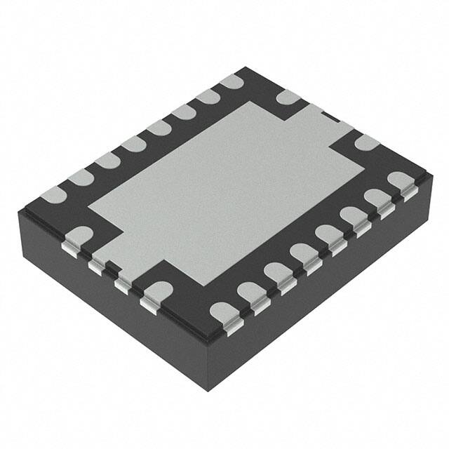
TCAN4550
BODY SIZE (NOM)
VQFN (20)
4.50 mm x 3.50 mm
(1) For all available packages, see the orderable addendum at
the end of the data sheet.
Simplified Schematics, CLKIN from MCU
Simplified Schematics, Crystal
3k
3k
10 µF
10 µF
VBAT
10 nF
330 nF
100 nF
VBAT
10 µF
EN
VIN
VCCOUT
FLTR
VINT
VLVRX
VIO
LDO(s)
VOUT
CNTL
VIO
10 µF
POR
Under
Voltage
GPIO3
VCC
Reset
SCLK
MOSI
MISO
CLKOUT
OSC2
nCS
GPIO2
GPIO1
GPIO
VSUP
VINT
nWKRQ
TX/RX Data
Buffer
RST
SCLK
SDI
SDO
nCS
GPO2
nINT
GPIO1
SPI slave,
System
Controller
OSC1
VCC
GPIO3
2-wire
CAN
bus
MCU
OSC2
VINT
nWKRQ
Under
Voltage
Optional:
Filtering,
Transient and
ESD
Filter
TCAN4550
TXD_INT
TX/RX Data
Buffer
VIO
Optional:
Terminating
Node
GND
POR
VCCINT2
VLVRX for LP
RX
CAN-FD
Transceiver
VINT
VLVRX
VIO
100 nF
CANH
CANL
20 MHz
CNTL
VIO
TX/RX CAN-FD
Controller with
Filters
RXD_INT
WAKE
VCCOUT
LDO(s)
TCAN4550
VCCINT1
FLTR
INH
VOUT
10 µF
VIO
MCU
Filter
TXD_INT
33 k
10 µF
EN
Voltage
Regulator
(e.g.
TPSxxxx)
100 nF
VCCINT2
OSC1
WAKE
INH
330 nF
100 nF
VIN
VSUP
Voltage
Regulator
(e.g.
TPSxxxx)
10 nF
33 k
Reset
SCLK
MOSI
MISO
nCS
GPIO2
GPIO1
GPIO
RST
SCLK
SDI
SDO
nCS
GPO2
nINT
GPIO1
SPI slave,
System
Controller
VCCINT1
CANH
VLVRX for LP
RX
TX/RX CAN-FD
Controller with
Filters
RXD_INT
2-wire
CAN
bus
CAN-FD
Transceiver
CANL
Optional:
Terminating
Node
GND
OSC1
OSC2
40 MHz
Optional:
Filtering,
Transient and
ESD
1
An IMPORTANT NOTICE at the end of this data sheet addresses availability, warranty, changes, use in safety-critical applications,
intellectual property matters and other important disclaimers. PRODUCTION DATA.
�TCAN4550
SLLSF91A – DECEMBER 2018 – REVISED JANUARY 2020
www.ti.com
Table of Contents
1
2
3
4
5
6
Features ..................................................................
Applications ...........................................................
Description .............................................................
Revision History.....................................................
Pin Configuration and Functions .........................
Specifications.........................................................
1
1
1
2
3
4
6.1 Absolute Maximum Ratings ...................................... 4
6.2 ESD Ratings.............................................................. 4
6.3 ESD Ratings, IEC ESD and ISO Transient
Specification............................................................... 4
6.4 Recommended Operating Conditions....................... 5
6.5 Thermal Information .................................................. 5
6.6 Supply Characteristics .............................................. 5
6.7 Electrical Characteristics........................................... 6
6.8 Timing Requirements ................................................ 9
6.9 Switching Characteristics .......................................... 9
6.10 Typical Characteristics .......................................... 11
7
8
Parameter Measurement Information ................ 11
Detailed Description ............................................ 20
8.1 Overview ................................................................. 20
8.2 Functional Block Diagram ....................................... 21
8.3
8.4
8.5
8.6
9
Feature Description.................................................
Device Functional Modes........................................
Programming ..........................................................
Register Maps .........................................................
24
27
41
44
Application and Implementation ...................... 127
9.1 Application Design Consideration ......................... 127
9.2 Typical Application ............................................... 131
10 Power Supply Recommendations ................... 134
11 Layout................................................................. 135
11.1 Layout Guidelines ............................................... 135
11.2 Layout Example .................................................. 136
12 Device and Documentation Support ............... 137
12.1 Documentation Support .....................................
12.2 Receiving Notification of Documentation
Updates..................................................................
12.3 Support Resources .............................................
12.4 Trademarks .........................................................
12.5 Electrostatic Discharge Caution ..........................
12.6 Glossary ..............................................................
137
137
137
137
137
138
13 Mechanical, Packaging, and Orderable
Information ......................................................... 138
4 Revision History
NOTE: Page numbers for previous revisions may differ from page numbers in the current version.
Changes from Original (December 2018) to Revision A
Page
•
Changed description of the GPO1 pin From: Configurable input/output function... To: Configurable output function........... 3
•
Deleted VCCOUT Supply Current from the Absolute Maximum Ratings ................................................................................... 4
•
Changed footnote Gauranteed to Specied throughout the electric table. .............................................................................. 6
•
Changed VIO value IIL for SDI, SCK and nCS inputs in test conditions cell from 0 V to 5.25 V............................................. 8
•
Changed MIN value of VOH for nWKRQ from 3 V to 2.8 V..................................................................................................... 8
•
Added VIO values for tSOV...................................................................................................................................................... 11
•
Changed Power Up Timing diagram VSUP ramp voltage level for INH turn on and timing. .............................................. 16
•
Deleted CLKOUT from the GPIO1 circuit in Figure 20......................................................................................................... 23
•
Deleted CLKOUT information from the GPO1 Pin section................................................................................................... 26
•
Deleted CLKOUT from the GPIO1 pin in Figure 28 ............................................................................................................. 33
•
Deleted CLKOUT from the GPIO1 pin in Figure 29 ............................................................................................................. 33
•
Deleted CLKOUT: Off from Sleep Mode section in Figure 32.............................................................................................. 34
•
Deleted CLKOUT: Off From Sleep Mode section in Figure 33 ............................................................................................ 35
•
Deleted GPO1_CONFIG from bits 15 and 14 in Figure 41 .................................................................................................. 50
•
Deleted bits 15 and 14 from GPO1_CONFIG from in Table 15 ........................................................................................... 51
•
Changed CLKOUT_GPIO1_CONFIG To: GPIO1_CONFIG for GPO1_CONFIG in Table 15 ............................................. 51
•
Changed the name of offset 1048 From: TDCE To: TDCR ................................................................................................ 63
•
Added INH Brownout Behavior section in Application section. ......................................................................................... 130
2
Submit Documentation Feedback
Copyright © 2018–2020, Texas Instruments Incorporated
Product Folder Links: TCAN4550
�TCAN4550
www.ti.com
SLLSF91A – DECEMBER 2018 – REVISED JANUARY 2020
5 Pin Configuration and Functions
OSC1
OSC2
1
20
RGY Package
20 Pin (VQFN)
Top View
nWKRQ
2
19
RS T
GPIO1
3
18
FL TR
SCLK
4
17
VIO
Th ermal
SDI
5
16
VCCOUT
SDO
6
15
INH
nCS
7
14
VSUP
nINT
8
13
GND
GPO2
9
12
WAK E
11
CA NH
CA NL
10
Pad
No t to scale
Pin Functions
PIN
TYPE (1)
DESCRIPTION
NO.
NAME
1
OSC1
2
nWKRQ
DO
Wake request (active low)
3
GPO1
DO
Configurable output function pin through SPI
4
SCLK
DI
SPI clock input
5
SDI
DI
SPI slave data input from master output
6
SDO
DO
SPI slave data output to master input
7
nCS
DI
SPI chip select
8
nINT
DO
Interrupt pin to MCU (active low)
9
GPO2
DO
Configurable output function pin through SPI
10
CANL
HV Bus I/O
Low level CAN bus line
11
CANH
HV Bus I/O
High level CAN bus line
12
WAKE
HVI
Wake input, high voltage input
13
GND
GND
Ground connection
14
VSUP
HV Supply
In
Supply from battery
15
INH
16
VCCOUT
17
VIO
18
FLTR
—
Internal regulator filter, requires external capacitor to ground
19
RST
DI
Device reset
20
OSC2
O
External crystal oscillator output; when using single input clock to OSC1 this pin should be connected to ground
(1)
I
HVO
Supply Out
Supply In
External crystal oscillator or clock input
Inhibit to control system voltage regulators and supplies (open drain)
5 V regulated output
Digital I/O voltage supply
Note: DI = Digital Input; DO = Digital Output; HV = High Voltage; Thermal PAD and GND Pins must be soldered to GND
Submit Documentation Feedback
Copyright © 2018–2020, Texas Instruments Incorporated
Product Folder Links: TCAN4550
3
�TCAN4550
SLLSF91A – DECEMBER 2018 – REVISED JANUARY 2020
www.ti.com
6 Specifications
6.1 Absolute Maximum Ratings
over operating free-air temperature range for – 40 ℃ ≤ TA ≤ 125 ℃ (unless otherwise noted) (1)
MIN
MAX
VSUP
Supply voltage
–0.3
42
V
VIO
Supply voltage I/O level shifter
–0.3
6
V
VCCOUT
5 V output supply
–0.3
6
V
VBUS
CAN bus I/O voltage (CANH, CANL)
–42
42
V
VWAKE
WAKE pin input voltage
–0.3
42
V
VINH
Inhibit pin output voltage
–0.3
42
V
VLogic_Input
Logic input terminal voltage
–0.3
6
V
VSO
Digital output terminal voltage
–0.5
6
V
IO(SO)
Digital output current
8
mA
IO(INH)
Inhibit output current
4
mA
IO(WAKE)
Wake current if due to ground shift V(WAKE) ≤ V(GND) – 0.3 V
3
mA
TJ
Junction temperature
–40
150
°C
Tstg
Storage temperature
–65
150
°C
(1)
UNIT
Stresses beyond those listed under Absolute Maximum Rating may cause permanent damage to the device. These are stress ratings
only, which do not imply functional operation of the device at these or any other conditions beyond those indicated under Recommended
Operating Condition. Exposure to absolute-maximum-rated conditions for extended periods may affect device reliability.
6.2 ESD Ratings
VALUE
UNIT
V(ESD)
Electrostatic discharge
Human body model (HBM) classification level 3A per AEC Q100-002 All
terminal except for CANH and CANL. WAKE terminals which are with
respect to ground only (1)
±4000
V
V(ESD)
Electrostatic discharge
Human body model (HBM) classification level H2 for CANH and
CANL (1)
±12000
V
V(ESD)
Electrostatic discharge
Charged device model (CDM)
classification level C5, per AEC
Q100-011
±750
V
(1)
All terminals
Terminals stressed with respect to GND
6.3 ESD Ratings, IEC ESD and ISO Transient Specification
V(ESD)
V(ESD)
Electrostatic discharge according to IBEE CAN
EMC (1)
Contact discharge
Electrostatic discharge according to SAEJ29622 (2)
Contact discharge
ISO7637 Transients according to IBEE CAN EMC test spec
CAN bus terminals (CANH and CANL), VSUP and WAKE (3)
(1)
(2)
(3)
4
Air discharge
Air discharge
VALUE
UNIT
±8000
V
±15 000
V
±8000
±15 000
Pulse 1
-100
Pulse 2
75
Pulse 3a
-150
Pulse 3b
100
V
IEC 61000-4-2 is a system-level ESD test. Results given here are specific to the IBEE LIN EMC Test specification conditions per IEC TS
62228. Different system-level configurations may lead to different results
SAEJ2962-2 Testing performed at 3rd party US3 approved EMC test facility, test report available upon request.
ISO7637 is a system-level transient test. Results given here are specific to the IBEE CAN EMC Test specification conditions. Different
system-level configurations may lead to different results.
Submit Documentation Feedback
Copyright © 2018–2020, Texas Instruments Incorporated
Product Folder Links: TCAN4550
�TCAN4550
www.ti.com
SLLSF91A – DECEMBER 2018 – REVISED JANUARY 2020
6.4 Recommended Operating Conditions
over operating free-air temperature range for – 40 ℃ ≤ TA ≤ 125 ℃ (unless otherwise noted)
MIN
VSUP
Supply voltage
VIO
Logic pin supply voltage
IOH(DO)
Digital terminal high-level output current
IOL(DO)
Digital terminal low-level output current
IO (INH)
INH output current
C(FLTR)
Filter pin capacitance See Power Supply Recommendations
C(VCCOUT)
VCCOUT supply capacitance See Power Supply Recommendations
CWAKE
External WAKE pin capacitance
TSDR
Thermal shutdown rising
TSDF
Thermal shutdown falling
TSD(HYS)
Thermal shutdown hysteresis
TYP
MAX
6
24
3.135
5.25
UNIT
V
V
–2
mA
2
mA
1
mA
300
nF
10
µF
10
nF
℃
160
℃
150
℃
10
6.5 Thermal Information
TCAN4550
THERMAL METRIC
(1)
PKG DES (RGY)
UNIT
20 PINS
RθJA
Junction-to-ambient thermal resistance
35.2
°C/W
RθJC(top)
Junction-to-case (top) thermal resistance
28.1
°C/W
RθJB
Junction-to-board thermal resistance
12.8
°C/W
ΨJT
Junction-to-top characterization parameter
0.3
°C/W
ΨJB
Junction-to-board characterization parameter
12.7
°C/W
RθJC(bot)
Junction-to-case (bottom) thermal resistance
1.1
°C/W
(1)
For more information about traditional and new thermal metrics, see the Semiconductor and IC Package Thermal Metrics application
report.
6.6 Supply Characteristics
over operating free-air temperature range for – 40 ℃ ≤ TA ≤ 125 ℃ (unless otherwise noted)
PARAMETER
TEST CONDITIONS
MAX
UNIT
mA
See Figure 5 RL = 50 Ω, CL =
open, high bus load. VCCOUT =
no load
90
mA
Dominant with bus fault
See Figure 5 CANH = - 25 V,
RL = open, CL = open VCCOUT
= no load
180
mA
Recessive
See Figure 5 RL = 60 Ω, CL =
open, RCM = open, VCCOUT =
no load
15
mA
See Figure 5 RL = 60 Ω, CL =
open, -40°C < TA < 85°C,
VCCOUT = no load, CANH/L
terminated to 2.5 V
3.5
mA
See Figure 5 RL = 60 Ω, CL =
open, -40°C < TA < 85°C,
VCCOUT = no load CANH/L
terminated to GND ± 100 mV
3.4
mA
42
µA
Supply current, normal mode
Supply current, standby mode
ISUP
TYP
80
Dominant
ISUP
MIN
See Figure 5 RL = 60 Ω, CL =
open. typical bus load. VCCOUT
= no load
Supply current, sleep mode
SPI bus, OSC/CLKIN disabled:
-40°C < TA < 85°C, VIO = 0
25
Submit Documentation Feedback
Copyright © 2018–2020, Texas Instruments Incorporated
Product Folder Links: TCAN4550
5
�TCAN4550
SLLSF91A – DECEMBER 2018 – REVISED JANUARY 2020
www.ti.com
Supply Characteristics (continued)
over operating free-air temperature range for – 40 ℃ ≤ TA ≤ 125 ℃ (unless otherwise noted)
PARAMETER
TEST CONDITIONS
IVIO
I/O supply current normal
mode dominant
I/O supply current
IVIO
I/O supply current, sleep mode
I/O supply current
IVCCOUT
VCCOUT supply current
UVSUP
UVIO
tUV/TSD
(1)
(2)
MIN
TYP
800
µA
Crystal = 40 MHz, VIO = 5 V
3
mA
Sleep Mode VIO = 5 V; OSC1 =
CLKIN = 0 V and OSC2 = GND
9
µA
70
mA
5.9
V
(1)
Under voltage detection on VSUP rising ramp for protected
mode
Under voltage detection on VSUP falling ramp for protected
mode
Under voltage detection on VIO rising ramp for protected
mode
Under voltage detection on VIO falling ramp for protected
mode
(2)
UNIT
CLKIN = 40 MHz, VIO = 5 V
Normal Mode: VCCOUT = 5 V;
-40°C < TA < 85°C See
Section VCCOUT Pin
Under voltage filter time and thermal shutdown timer
MAX
5.5
See Section Under Voltage
Lockout (UVLO) and
Unpowered Device
4.5
4.7
2.45
See Section Under Voltage
Lockout (UVLO) and
Unpowered Device
2.1
Upon a UVIO event this timer
starts and provides time for VIO
input to return. See section
Thermal Shutdown for
description of thermal shut
down.
V
2.6
2.25
200
V
V
500
ms
When a crystal is used this current will be higher until the crystal's capacitors bleed off their energy. How much current and length of
time to bleed of the energy is system dependent and will not be specified.
Specified by design
6.7 Electrical Characteristics
over operating free-air temperature range for – 40 ℃ ≤ TA ≤ 125 ℃ (unless otherwise noted)
PARAMETER
TEST CONDITIONS
(1)
MIN
TYP
MAX
UNIT
CAN DRIVER ELECTRICAL CHARACTERISTICS
Bus output voltage (dominant) CANH
VO(D)
Bus output voltage (dominant) CANL
See Figure 5 and Figure 6, TXD_INT = 0
V, EN = 0 V, 50 Ω ≤ RL ≤ 65 Ω, CL =
open, RCM = open
2.75
4.5
V
0.5
2.25
V
3
V
–5.0
10
V
–0.1
0.1
V
–0.1
0.1
V
–0.2
0.2
V
See Figure 3 and Figure 6, TXD_INT = 0
V, 50 Ω ≤ RL ≤ 65 Ω, CL = open, RCM =
open
1.5
3
V
See Figure 3 and Figure 6, TXD_INT = 0
V, 45 Ω ≤ RL ≤ 70 Ω, CL = open, RCM =
open
1.4
3
V
See Figure 3 and Figure 6, TXD_INT = 0
V, RL = 2.24 kΩ, CL = open, RCM = open
1.5
5
V
VO(R)
Bus output voltage (recessive)
See Figure 3 and Figure 6, TXD_INT =
VIO, RL = open (no load), RCM = open
V(DIFF)
Maximum differential voltage rating
See Figure 3 and Figure 6
Bus output voltage (Standby Mode)
CANH
VO(STB)
Bus output voltage (Standby Mode)
CANL
See Figure 3 and Figure 6, TXD_INT =
VIO, RL = open (no load), RCM = open
Bus output voltage (Standby Mode)
CANH - CANL
VOD(D)
(1)
6
Differential output voltage (dominant)
2
2.5
All TXD_INT, RXD_INT and EN_INT references are for internal nodes that represent the same functions for a physical layer transceiver.
Submit Documentation Feedback
Copyright © 2018–2020, Texas Instruments Incorporated
Product Folder Links: TCAN4550
�TCAN4550
www.ti.com
SLLSF91A – DECEMBER 2018 – REVISED JANUARY 2020
Electrical Characteristics (continued)
over operating free-air temperature range for – 40 ℃ ≤ TA ≤ 125 ℃ (unless otherwise noted)
PARAMETER
VOD(R)
TEST CONDITIONS
Differential output voltage (recessive)
(1)
MIN
TYP
MAX
UNIT
See Figure 3 and Figure 6, TXD_INT =
VIO, RL = 60 Ω, CL = open, RCM = open
–120
12
mV
See Figure 3 and Figure 6, TXD_INT =
VIO, RL = open (no load), CL = open,
RCM = open
–50
50
mV
VSYM
Output symmetry (dominant or
recessive)
( VO(CANH) + VO(CANL)) / VCC
See Figure 3 and Figure 6, RL = 60 Ω,
CL = open, RCM = open, C1 = 4.7 nF,
TXD_INT - 250 kHZ, 1 MHz
0.9
1.1
V/V
VSYM_DC
Output symmetry (dominant or
recessive) (VCC – VO(CANH) –
VO(CANL)) with a frequency that
corresponds to the highest bit rate for
which the HS-PMA implementation is
intended, however, at most 1 MHz (2
Mbit/s)
See Figure 3 and Figure 6, RL = 60 Ω,
CL = open, RCM = open, C1 = 4.7 nF
–300
300
mV
See Figure 3 and Figure 10, -3.0 V ≤
VCANH ≤ 18.0 V, CANL = open, TXD_INT
=0V
–100
IOS_DOM
IOS_REC
Short-circuit steady-state output current,
dominant
Short-circuit steady-state output current,
recessive
mA
See Figure 3 and Figure 10, -3.0 V ≤
VCANL ≤+18.0 V, CANH = open,
TXD_INT = 0 V
See Figure 3 and Figure 10, – 27 V ≤
VBUS ≤ 32 V, VBUS = CANH = CANL
100
mA
–5
5
mA
0.9
8
V
–3.0
0.5
V
CAN RECEIVER ELECTRICAL CHARACTERISTICS
VITrec
Receiver dominant state differential input
-12.0 V ≤ VCANL ≤ +12.0 V
voltage range, bus biasing active
-12.0 V ≤ VCANH ≤ +12.0 V See
Receiver recessive state differential input Figure 7, Table 3
voltage range bus biasing active
VHYS
Hysteresis voltage for input-threshold,
normal modes
VIT(ENdom)
Receiver dominant state differential input -12.0 V ≤ VCANL ≤ +12.0 V
voltage range, bus biasing inactive
-12.0 V ≤ VCANH ≤ +12.0 V See
(VDiff)
Figure 7, Table 3
1.15
8
V
VIT(ENrec)
Receiver recessive state differential input -12.0 V ≤ VCANL ≤ +12.0 V
voltage range, bus biasing inactive
-12.0 V ≤ VCANH ≤ +12.0 V See
(VDiff)
Figure 7, Table 3
–3
0.4
V
VCM
Common mode range: normal
See Figure 7, Table 3
–12
12
V
VCM(EN)
Common mode range: standby mode
See Figure 7, Table 3
–12
12
V
IIOFF(LKG)
Power-off (unpowered) bus input
leakage current
VCANH = VCANL = 5 V, Vsup to GND via 0
Ω and 47 kΩ resistor
5
µA
CI
Input capacitance to ground (CANH or
CANL)
25
pF
CID
Differential input capacitance
14
pF
VITdom
See Figure 7, Table 3
120
mV
RID
Differential input resistance
TXD_INT = VCCINT, normal mode: -2.0 V
≤ VCANH ≤+7.0 V; -2.0 V ≤VCANL ≤ + 7.0
V
RIN
Single ended Input resistance (CANH or
CANL)
-2.0 V ≤ VCANH ≤+7.0 V; -2.0 V ≤VCANL ≤
+ 7.0 V
30
50
kΩ
RIN(M)
Input resistance matching: [1 –
(RIN(CANH) / (RIN(CANL))] × 100%
VCANH = VCANL = 5.0 V
–1
1
%
VCCOUT
5 V output supply
ICCOUT = -70 mA to 0 mA; VSUP = 6 V to
18 V; -40°C < TA < 85°C
5
5.25
V
VDROP
Drop out voltage
VCCOUT = 5 V, VSUP = 12 V, ICCOUT = 70
mA
300
500
mV
ΔVCC(ΔVSUP)
Line regulation
VSUP = 6 V to 24 V, ΔVCCOUT, ICCOUT =
10 mA
50
mV
60
100
kΩ
4.75
Submit Documentation Feedback
Copyright © 2018–2020, Texas Instruments Incorporated
Product Folder Links: TCAN4550
7
�TCAN4550
SLLSF91A – DECEMBER 2018 – REVISED JANUARY 2020
www.ti.com
Electrical Characteristics (continued)
over operating free-air temperature range for – 40 ℃ ≤ TA ≤ 125 ℃ (unless otherwise noted)
PARAMETER
ΔVCC(ΔVSUPL)
Load regulation
UVCCOUT
Under voltage threshold on VCCOUT
TEST CONDITIONS
(1)
MIN
TYP
VSUP = 14 V, ICCOUT = 1 mA to 70
mA, ΔVCCOUT, –40℃ ≤ TA ≤ 125℃
MAX
60
4.2
4.55
UNIT
mV
V
FLTR TERMINAL
VMEASURE
Voltage measured at FLTR pin
C(FLTR)
Filter pin capacitor
External filter capacitor
300
1.5
V
330
nF
INH OUTPUT TERMINAL (HIGH VOLTAGE OUTPUT)
ΔVH
High-level voltage drop INH with respect
to VSUP
IINH = - 0.5 mA
ILKG(INH)
Leakage current
INH = 0 V, Sleep Mode
0.5
–0.5
1
V
0.7
µA
WAKE INPUT TERMINAL (HIGH VOLTAGE INPUT)
VIH
High-level input voltage
Standby mode, WAKE pin enabled
VIL
Low-level input voltage
Standby mode, WAKE pin enabled
IIH
High-level input current
WAKE = VSUP–1 V
IIL
Low-level input current
WAKE = 1 V
WAKE filter time
Wake up filter time from a wake edge on
WAKE; standby, sleep mode
tWAKE
VSUP–2
V
VSUP–3
–25
–15
15
V
µA
25
50
µA
µs
SDI, SCK, GPIO1 INPUT TERMINALS
VIH
High-level input voltage
VIL
Low-level input voltage
0.7
IIH
High-level input leakage current
Inputs = VIO = 5.25 V
IIL
Low-level input leakage current
Inputs = 0 V, VIO = 5.25 V
CIN
Input capacitance
18 MHz
ILKG(OFF)
Unpowered leakage current (SDI and
SCK only)
Inputs = 5.25 V, VIO = VSUP = 0 V
VIO
–1
–100
10
–1
0.3
VIO
1
µA
–5
µA
12
pF
1
µA
nCS INPUT TERMINAL
VIH
High-level input voltage
0.7
VIO
VIL
Low-level input voltage
0.3
VIO
IIH
High-level input leakage current
nCS = VIO = 5.25 V
–1
1
µA
IIL
Low-level input leakage current
nCS = VIO = 5.25 V
–50
–5
µA
ILKG(OFF)
Unpowered leakage current
nCS = 5.25 V, VIO = VSUP = 0 V
–1
1
µA
RST INPUT TERMINAL
VIH
High-level input voltage
VIL
Low-level input voltage
0.7
IIH
High-level input leakage current
RST = VIO = 5.25 V
IIL
Low-level input leakage current
RST = 0 V
ILKG(OFF)
Unpowered leakage current
RST = VIO, VSUP = 0 V
tPULSE_WIDTH
Width of the input pulse
VIO
0.3
VIO
1
10
µA
–1
1
µA
–7.5
7.5
µA
30
µs
SDO, GPIO1, GPO2 OUTPUT TERMINAL; nINT (OPEN DRAIIN) and nWKRQ (WHEN PROGRAMMED TO WORK OFF OF VIO AND IS
OPEN DRAIN)
VOH
High-level output voltage
VOL
Low-level output voltage
0.8
VIO
0.2
VIO
3.6
V
0.7
V
nWKRQ OUTPUT TERMINAL (DEFAULT INTERNAL VOLTAGE RAIL)
VOH
High-level output voltage
Default value when based upon internal
voltage rail
VOL
Low-level output voltage
Default value when based upon internal
voltage rail
2.8
OSC1 TERMINAL AND CRYSTAL SPECIFICATION
8
Submit Documentation Feedback
Copyright © 2018–2020, Texas Instruments Incorporated
Product Folder Links: TCAN4550
�TCAN4550
www.ti.com
SLLSF91A – DECEMBER 2018 – REVISED JANUARY 2020
Electrical Characteristics (continued)
over operating free-air temperature range for – 40 ℃ ≤ TA ≤ 125 ℃ (unless otherwise noted)
PARAMETER
TEST CONDITIONS
(1)
MIN
TYP
UNIT
1.10
VIO
0.3
VIO
VIH
High-level input voltage
VIL
Low-level input voltage
FOSC1
Clock-In frequency tolerance , see
section Crystal and Clock Input
Requirements
20 MHz
–0.5
0.5
%
FOSC1
Clock-In frequency tolerance, see
section Crystal and Clock Input
Requirements
40 MHz
–0.5
0.5
%
tDC
Input duty cycle
45
55
%
ESR
Crystal ESR for load capacitance
60
Ω
(2)
0.85
MAX
(2)
Specified by design
6.8 Timing Requirements
over operating free-air temperature range for – 40 ℃ ≤ TA ≤ 125 ℃ (unless otherwise noted)
MIN
TYP
MAX
UNIT
MODE CHANGE TIMES (FULL DEVICE)
tMODE_STBY_NOM
Standby to normal mode change time based upon SPI
write
70
µs
tMODE_NOM_SLP
SPI write to go to Sleep from Normal: INH and nWKRQ
turned off, See Figure 17
200
µs
tMODE_SLP_STBY
WUP or LWU event until INH and nWKRQ asserted, See
Figure 16
200
µs
tMODE_SLP_STBY_VCCOUT_ON
WUP or LWU event until VCCOUT on, See Figure 16
1.5
ms
tMODE_NOM_STBY
SPI write to go to standby from normal mode,
See Figure 18
200
µs
6.9 Switching Characteristics
over operating free-air temperature range for – 40 ℃ ≤ TA ≤ 125 ℃ (unless otherwise noted)
PARAMETER
TEST CONDITIONS
MIN
TYP
MAX
UNIT
50
85
110
ns
35
75
100
ns
SWITCHING CHARACTERISTICS (CAN TRANSCEIVER ONLY)
tpHR
Propagation delay time, high TXD_INT to
Driver Recessive (1)
tpLD
Propagation delay time, low TXD_INT to
driver dominant (1)
tsk(p)
Pulse skew (|tpHR – tpLD|)
tR/F
Differential output signal rise time:
tpRH
Propagation delay time, bus recessive
input to high RXD_INT output
tpDL
Propagation delay time, bus dominant
input to RXD_INT low output
See Figure 6, RST = 0 V. Typical
conditions: RL = 60 Ω, CL = 100 pF, RCM
= open
See Figure 7, typical conditions: CANL =
1.5 V, CANH = 3.5 V.
30
40
ns
8
55
75
ns
35
55
90
ns
35
55
90
ns
235
ns
1.8
µs
DEVICE SWITCHING CHARACTERISTICS
tLOOP
Loop delay (2)(CAN transceiver only)
See Figure 8, RST = 0 V. typical
conditions: RL = 60 Ω, CL = 100 pF,
CRXD = 15 pF
tWK_FILTER
Bus time to meet filtered bus
requirements for wake up request
See Figure 24, standby mode.
(1)
(2)
0.5
All TXD_INT, RXD_INT, EN_INT and CAN transceiver only references are for internal nodes that represent the same functions for a
stand-alone transceiver.
Time span from signal edge on TXD_INT input to next signal edge with same polarity on RXD output, the maximum of delay of both
signal edges is to be considered.
Submit Documentation Feedback
Copyright © 2018–2020, Texas Instruments Incorporated
Product Folder Links: TCAN4550
9
�TCAN4550
SLLSF91A – DECEMBER 2018 – REVISED JANUARY 2020
www.ti.com
Switching Characteristics (continued)
over operating free-air temperature range for – 40 ℃ ≤ TA ≤ 125 ℃ (unless otherwise noted)
PARAMETER
TEST CONDITIONS
tWK_TIMEOUT
Bus wake-up timeout: time that a WUP
must take place within to be considered
valid
tSILENCE
Timeout for bus inactivity
tINACTIVE
Time required for the processor to clear
wake flag or put the device into normal
mode upon power up, power on reset or
after wake event otherwise the device
will enter sleep mode (3)
tBias
Time from the start of a dominantrecessive-dominant sequence
(3)
(3)
tPower_Up
Power up time on VSUP
tTXD_INT_DTO
Dominant time out (4) (CAN transceiver
only) (1)
MIN
TYP
MAX
UNIT
See Figure 24
0.8
2.9
ms
Timer is reset and restarted when bus
changes from dominant to recessive or
vice versa.
0.6
1.2
s
2
6
min
Each phase 6 µs until Vsym ≥ 0.1.
See Figure 12
250
µs
See Figure 15
250
µs
1
5
ms
435
530
ns
155
210
ns
80
135
ns
400
550
ns
120
220
ns
80
135
ns
See Figure 25, RL = 60 Ω, CL = open
4
TRANSMITTER AND RECEIVER SWITCHING CHARACTERISTICS
tBit(Bus)2M
Transmitted recessive bit width @ 2
Mbps
tBit(Bus)5M
Transmitted recessive bit width @ 5
Mbps
tBit(Bus)8M (5)
Transmitted recessive bit width @ 8
Mbps
tBit(RXD)2M
Received recessive bit width @ 2 Mbps
tBit(RXD)5M
Received recessive bit width @ 5 Mbps
tBit(RXD)8M (5)
Received recessive bit width @ 8 Mbps
ΔtRec (6)
See Figure 7, RST = 0 V typical
conditions: RL = 60 Ω, CL = 100 pF,
CRXD = 15 pF
See Figure 7, RST = 0 V typical
conditions: RL = 60 Ω, CL = 100 pF,
CRXD = 15 pF
Receiver Timing symmetry @ 2 Mbps
Receiver Timing symmetry @ 5 Mbps
See Figure 7, RST = 0 V typical
conditions: RL = 60 Ω, CL = 100 pF,
CRXD = 15 pF,
See Figure 7, RST = 0 V typical
conditions: RL = 60 Ω, CL = 100 pF,
CRXD = 15 pF
See Figure 7, RST = 0 V typical
conditions: RL = 60 Ω, CL = 100 pF,
CRXD = 15 pF
–65
30
40
ns
–45
5
15
ns
18
MHz
SPI SWITCHING CHARACTERISTICS
fSCK
SCK, SPI clock frequency
tSCK
SCK, SPI clock period
tRSCK
SCK rise time
(3)
(3)
SCK fall time
tSCKH
SCK, SPI clock high
tSCKL
SCK, SPI clock low
(3)
(3)
Chip select setup time
tCSH
Chip select hold time
tCSD
Chip select disable time
tSISU
Data in setup time
tSIH
Data in hold time
10
56
See Figure 13
(3)
tCSS
(5)
(6)
See Figure 14
See Figure 13
tFSCK
(3)
(4)
(3)
(3)
(3)
(3)
(3)
(3)
ns
10
ns
10
ns
See Figure 14
18
ns
See Figure 14
18
ns
See Figure 13
28
ns
See Figure 13
28
ns
See Figure 13
125
ns
See Figure 13
5
ns
See Figure 13
10
ns
Specified by design
The TXD_INT dominant time out (tTXD_INT_DTO) disables the driver of the transceiver once the TXD_INT has been dominant longer than
tTXD_INT_DTO, which releases the bus lines to recessive, preventing a local failure from locking the bus dominant. The driver may only
transmit dominant again after TXD_INT has been returned HIGH (recessive). While this protects the bus from local faults, locking the
bus dominant, it limits the minimum data rate possible. The CAN protocol allows a maximum of eleven successive dominant bits (on
TXD_INT) for the worst case, where five successive dominant bits are followed immediately by an error frame. This, along with the
tTXD_INT_DTO minimum, limits the minimum bit rate. The minimum bit rate may be calculated by: Minimum Bit Rate = 11/ tTXD_INT_DTO =
11 bits / 1.2 ms = 9.2 kbps.
Characterized but not 100% tested
ΔtRec = tBit(RXD) – tBit(Bus)
Submit Documentation Feedback
Copyright © 2018–2020, Texas Instruments Incorporated
Product Folder Links: TCAN4550
�TCAN4550
www.ti.com
SLLSF91A – DECEMBER 2018 – REVISED JANUARY 2020
Switching Characteristics (continued)
over operating free-air temperature range for – 40 ℃ ≤ TA ≤ 125 ℃ (unless otherwise noted)
PARAMETER
tSOV
Data out valid
tRSO
SO rise time
tFSO
SO fall time
TEST CONDITIONS
(3)
(3)
(3)
MIN
TYP
MAX
UNIT
VIO = 3.135 V to 5.25 V, See Figure 14
20
ns
See Figure 14
10
ns
See Figure 14
10
ns
6.10 Typical Characteristics
38
105
-40 °C
25 °C
55 °C
85 °C
100 °C
125 °C
100
36
95
90
34
85
80
ISUP (mA)
ISUP (PA)
32
30
28
75
70
65
60
26
55
-40 °C
25 °C
55 °C
85 °C
100 °C
125 °C
24
22
50
45
40
20
35
6
8
10
12
14
16
18
20
22
VSUP (V)
VCCOUT = 0 V
24
6
8
10
12
14
CAN Bus Load = 60 Ω
16
18
20
22
VSUP (V)
D001
ICCOUT = 0 mA
VCCOUT = 5 V
Figure 1. ISUP vs VSUP Sleep Mode
24
D003
ICCOUT = 70 mA
CAN Transceiver Off
Figure 2. ISUP Current Across Temperature and VSUP LDO
Output Only.
7 Parameter Measurement Information
NOTE
All TXD_INT, RXD_INT and EN_INT references are for internal nodes that represent the
same functions for a physical layer transceiver. In test mode these can be brought out to
pins to test the transceiver or CAN FD controller.
Standby Mode (Low
Power)
Typical Bus Voltage
Normal Mode
CANH
Vdiff
Vdiff
CANL
Recessive
Dominant
Recessive
Time, t
Figure 3. Bus States (Physical Bit Representation)
Submit Documentation Feedback
Copyright © 2018–2020, Texas Instruments Incorporated
Product Folder Links: TCAN4550
11
�TCAN4550
SLLSF91A – DECEMBER 2018 – REVISED JANUARY 2020
www.ti.com
Parameter Measurement Information (continued)
CANH
VCC/2
A
Bias
Unit
RXD_INT
B
CANL
Figure 4. Simplified Recessive Common Mode Bias Unit and Receiver
NOTE
A: Classic CAN and CAN FD modes
B: Standby and Sleep Modes (Low Power)
CANH
TXD_INT
CL
RL
CANL
Figure 5. Supply Test Circuit
RCM
CANH
VCC
50%
TXD_INT
50%
TXD_INT
RL
CL
0V
VCM
VOD
VO(CANH)
CANL
90%
RCM
VO(CANL)
tpHR
tpLD
0.9 V
VOD
0.5 V
10%
tR
tF
Figure 6. Driver Test Circuit and Measurement
12
Submit Documentation Feedback
Copyright © 2018–2020, Texas Instruments Incorporated
Product Folder Links: TCAN4550
�TCAN4550
www.ti.com
SLLSF91A – DECEMBER 2018 – REVISED JANUARY 2020
Parameter Measurement Information (continued)
CANH
1.5 V
RXD_INT
0.9 V
VID
IO
0.5 V
0V
VID
tpDL
tpRH
VOH
VO
CL_RXD_INT
CANL
90%
70%
VO(RXD_INT)
30%
10%
VOL
tF
tR
Figure 7. Receiver Test Circuit and Measurement
RCM
CANH
VI
TXD_INT
VI
VCM
CL
RL
tLOOP
Falling
edge
70%
TXD_INT
CANL
EN_INT
30%
30%
RCM
0V
0V
5 x tBIT(TXD_INT)
tBIT(TXD_INT)
RXD_INT
tBIT(Bus)
VO
CL_RXD_INT
900 mV
VDiff
500 mV
VOH
70%
RXD_INT
30%
tLOOP
rising
edge
VOL
tBIT(RXD_INT)
Figure 8. Transmitter and Receiver Timing Behavior Test Circuit and Measurement
CANH
VIH
TXD_INT
TXD_INT
RL
CL
30%
VOD
0V
VOD(D)
CANL
0.9 V
VOD
0.5 V
0V
tTXD_INT_DTO
Figure 9. TXD_INT Dominant Timeout Test Circuit and Measurement
Submit Documentation Feedback
Copyright © 2018–2020, Texas Instruments Incorporated
Product Folder Links: TCAN4550
13
�TCAN4550
SLLSF91A – DECEMBER 2018 – REVISED JANUARY 2020
www.ti.com
Parameter Measurement Information (continued)
200 s
IOS
CANH
TXD_INT
VBUS
IOS
VBUS
CANL
VBUS
0V
or
0V
VBUS
VBUS
Figure 10. Driver Short-Circuit Current Test and Measurement
VSUP
VSUP
VWAKE
INH
VSUP
VSUP - 2
VWAKE
VSUP - 3
0V
CVSUP
tWAKE
TCAN4550
OR
tWAKE
VWAKE
INH = H
INH = H
INH
INH
VSUP -1 V
VSUP -1 V
Figure 11. tWAKE While Monitoring INH Output
VDIFF
2.0 V
1.15 V
0.4 V
t > tWAKE_FILTER(MAX)
t > tWAKE_FILTER(MAX)
t > tWAKE_FILTER(MAX)
VSYM
0.1
tBias
Figure 12. Test Signal Definition for Bias Reaction Time Measurement
14
Submit Documentation Feedback
Copyright © 2018–2020, Texas Instruments Incorporated
Product Folder Links: TCAN4550
�TCAN4550
www.ti.com
SLLSF91A – DECEMBER 2018 – REVISED JANUARY 2020
Parameter Measurement Information (continued)
tCSD
nCS
tRSCK
tCSS
tCSH
tFSCK
SCLK
tSISU
SDI
tSIH
MSB In
LSB
In
SDO
Figure 13. SPI AC Characteristic Write
nCS
tSCK
tSCKL
tSCKH
SCLK
tSOV
tRSO
tFSO
SDO
LSB
Out
MSB Out
SDI
Figure 14. SPI AC Characteristic Read
Submit Documentation Feedback
Copyright © 2018–2020, Texas Instruments Incorporated
Product Folder Links: TCAN4550
15
�TCAN4550
SLLSF91A – DECEMBER 2018 – REVISED JANUARY 2020
www.ti.com
Parameter Measurement Information (continued)
14 V
VSUP
1.67 V to
4.14 V
~ 5.5 V
UVSUP
14 V
VSUP ± 1V
INH
tPower_Up
nWKRQ
VIO
VIO on and ramp time are system dependent and not specified
FLTR
VCCOUT
tMODE_SLP_STBY_VCCOUT_ON
UVCCOUT Cleared
Crystal/CLKIN
CLKIN is dependent on external source
and timing will not be specified
tCRYSTAL
VIO required for Crystal/CLKIN to work.
This is the stable internal clock.
STANDBY MODE
Transceiver Ready
nINT
Figure 15. Power Up Timing
16
Submit Documentation Feedback
Copyright © 2018–2020, Texas Instruments Incorporated
Product Folder Links: TCAN4550
�TCAN4550
www.ti.com
SLLSF91A – DECEMBER 2018 – REVISED JANUARY 2020
Parameter Measurement Information (continued)
14V
VSUP
Wake Event
WUP or LWU
14V
VSUP ± 1V
INH
tMODE_SLP_STBY
nWKRQ
VIO
VIO on and ramp time are system dependent and not specified
FLTR
VCCOUT
tMODE_SLP_STBY_VCCOUT_ON
UVCCOUT Cleared
Crystal/CLKIN
CLKIN is dependent on external source
and timing will not be specified
tCRYSTAL
VIO required for Crystal/CLKIN to work.
This is the stable internal clock.
STANDBY MODE
Transceiver Ready
nINT
Figure 16. Sleep to Standby Timing
Submit Documentation Feedback
Copyright © 2018–2020, Texas Instruments Incorporated
Product Folder Links: TCAN4550
17
�TCAN4550
SLLSF91A – DECEMBER 2018 – REVISED JANUARY 2020
www.ti.com
Parameter Measurement Information (continued)
14V
VSUP
SPI Mode
Change
Normal to
Sleep CMD
14V
VSUP ± 1V
INH
tMODE_NOM_SLP
nWKRQ
VIO
VIO off and ramp time are system dependent and not specified
FLTR
EN_VCCOUT_S
tSILENCE Expires
VCCOUT off ramp time is system dependent and not specified
VCCOUT
Crystal/CLKIN
Mode
120:6/3
VIO required for Crystal/CLKIN to work.
Normal Mode
Sleep Mode
Figure 17. Normal to Sleep Timing
18
Submit Documentation Feedback
Copyright © 2018–2020, Texas Instruments Incorporated
Product Folder Links: TCAN4550
�TCAN4550
www.ti.com
SLLSF91A – DECEMBER 2018 – REVISED JANUARY 2020
Parameter Measurement Information (continued)
14 V
VSUP
SPI Mode
Change
Normal to
Standby CMD
14 V
INH
nWKRQ
Low
High
VIO
FLTR
5V
VCCOUT
Crystal/CLKIN
Mode
120:6/3
Transceiver
Standby Mode
Normal Mode
tMODE_NOM_STBY
Figure 18. Normal to Standby Timing
Submit Documentation Feedback
Copyright © 2018–2020, Texas Instruments Incorporated
Product Folder Links: TCAN4550
19
�TCAN4550
SLLSF91A – DECEMBER 2018 – REVISED JANUARY 2020
www.ti.com
8 Detailed Description
8.1 Overview
The TCAN4550 is a CAN FD controller with an integrated CAN FD transceiver supporting data rates up to 5
Mbps. The CAN FD controller meets the specifications of the ISO 11898-1:2015 high speed Controller Area
Network (CAN) data link layer and meets the physical layer requirements of the ISO 11898-2:2016 High Speed
Controller Area Network (CAN) specification providing an interface between the CAN bus and the CAN protocol
controller supporting both classical CAN and CAN FD up to 5 megabits per second (Mbps). The TCAN4550
provides CAN FD transceiver functionality: differential transmit capability to the bus and differential receive
capability from the bus. The device includes many protection features providing device and CAN bus robustness.
The device can also wake up via remote wake up using CAN bus implementing the ISO 11898-2:2016 Wake Up
Pattern (WUP). Input/Output support for 3.3 V and 5 V microprocessors using VIO pin for seamless interface. The
TCAN4550 has a Serial Peripheral Interface (SPI) that connects to a local microprocessor for the device's
configuration; transmission and reception of CAN frames. The SPI interface supports clock rates up to 18 MHz.
The CAN bus has two logical states during operation: recessive and dominant. See Figure 3 and Figure 4.
In the recessive bus state, the bus is biased to a common mode of 2.5 V via the high resistance internal input
resistors of the receiver of each node. Recessive is equivalent to logic high. The recessive state is also the idle
state.
In the dominant bus state, the bus is driven differentially by one or more drivers. Current flows through the
termination resistors and generates a differential voltage on the bus. Dominant is equivalent to logic low. A
dominant state overwrites the recessive state.
During arbitration, multiple CAN nodes may transmit a dominant bit at the same time. In this case, the differential
voltage of the bus is greater than the differential voltage of a single driver.
Transceivers with low power Standby Mode have a third bus state where the bus terminals are weakly biased to
ground via the high resistance internal resistors of the receiver. See Figure 3 and Figure 4. The TCAN4550
supports auto biasing, see CAN Bus Biasing
The TCAN4550 has the ability to provide a single-ended clock output (GPIO1) based upon the crystal or singleended clock input on OSC1. Many of the pins can be configured for multiple purposes and are described in more
detail in Feature Description section. Much of the parametric data is based on internal links like the
TXD/RXD_INT which represent the TXD and RXD of a standalone CAN transceiver. The TCAN4550 has a test
mode that maps these signals to an external pin in order to perform compliance testing on the transceiver
(TXD/RXD_INT_PHY) and CAN core (TXD/RXD_INT_CAN) independently.
20
Submit Documentation Feedback
Copyright © 2018–2020, Texas Instruments Incorporated
Product Folder Links: TCAN4550
�TCAN4550
www.ti.com
SLLSF91A – DECEMBER 2018 – REVISED JANUARY 2020
8.2 Functional Block Diagram
VSUP
VCCOUT
FLTR
WAKE
INH
VINT
VLVRX
VIO
LDO(s)
CNTL
POR
VIO
Under
Voltage
Filter
TCAN4550
TXD_INT
VCCINT2
VINT
nWKRQ
TX/RX Data
Buffer
VIO
RST
SCLK
SDI
SDO
nCS
GPO2
nINT
GPIO1
SPI slave,
System
Controller
VCCINT1
CANH
VLVRX for LP
RX
TX/RX CAN-FD
Controller with
Filters
RXD_INT
CAN-FD
Transceiver
CANL
GND
OSC2
OSC1
40 MHz
•
•
•
•
NOTE
OSC1 pin is either a crystal or external clock input
When OSC1 is used as an external clock input pin OSC2 must be connected directly
to ground
When using an external clock input on OSC1 the input voltage should be the same as
the VIO voltage rail
The recommended crystal or clock rate to meet CAN FD 5 Mbps rates is 40 MHz
Submit Documentation Feedback
Copyright © 2018–2020, Texas Instruments Incorporated
Product Folder Links: TCAN4550
21
�TCAN4550
SLLSF91A – DECEMBER 2018 – REVISED JANUARY 2020
www.ti.com
Functional Block Diagram (continued)
VCCINT1
Transceiver Block Diagram
VSUP
TXD_INT
DOMINANT
TIME OUT
BIAS UNIT
TXD_INT_PHY
DRIVER
TXD_INT
CANH
CANL
Communication Bus
OVER
TEMP
EN_INT
MODE AND CONTROL LOGIC
VSUP
WAKE
WAKE
WAKE
INH_CNTL
UNDER
VOLTAGE
VSUP
INH
WAKE UP LOGIC /
MONITOR
RXD_INT_PHY
RXD_INT
RXD_INT
VLVRX
M
U
X
LOGIC
OUTPUT
Low Power Standby Bus
Receiver & Monitor
Figure 19. CAN Transceiver Block Diagram
22
Submit Documentation Feedback
Copyright © 2018–2020, Texas Instruments Incorporated
Product Folder Links: TCAN4550
�TCAN4550
www.ti.com
SLLSF91A – DECEMBER 2018 – REVISED JANUARY 2020
Functional Block Diagram (continued)
VIO
VIO
Chip
Reset
RST
VIO
SCLK
SCLK
VIO
SDI
SDI
VIO
SDO
SDO
VIO
nCS
GPI
VIO
RXD_INT_CAN
Test Mode
TXD_INT_PHY
GPI01
GPO
SPI & I/O
Controller
VIO
Test Mode
TXD_INT_CAN
GPO2
RXD_INT_PHY
GPO2 ± for all non test mode
VIO
Test Mode
nINT
EN_INT
3P6_SLEEP
WKRQ_3P6_SLEEP
nWKRQ
WKRQ_VIO
Figure 20. SPI and Digital IO Block Diagram
Submit Documentation Feedback
Copyright © 2018–2020, Texas Instruments Incorporated
Product Folder Links: TCAN4550
23
�TCAN4550
SLLSF91A – DECEMBER 2018 – REVISED JANUARY 2020
www.ti.com
8.3 Feature Description
8.3.1 VSUP Pin
This pin connects to the battery supply. It provides the supply to the internal regulators that support the digital
core, CAN transceiver and VCCOUT. This Pin requires a 100 nF capacitor at the pin. See Power Supply
Recommendations for more information. Upon power up; VSUP needs to rise above UVSUP rising threshold.
8.3.2 VIO Pin
The VIO pin provides the digital IO voltage to match the microprocessor IO voltage thus avoiding the
requirements for a level shifter. VIO supports IO pins SPI IO, GPO1 and GPO2. It also provides power to the
oscillator block supporting the crystal or CLKIN pins. It supports a range of 3.3 V to 5 V ± 5% nominal value
providing the widest range of controller support. This pin requires a 100 nF capacitor at the pin. See Power
Supply Recommendations for more information.
8.3.3 VCCOUT Pin
An internal LDO provides power for the integrated CAN transceiver and the VCCOUT pin for a total available
current of 125 mA. The amount of current that can be sourced is dependent upon the CAN transceiver
requirements during normal operation. When a bus fault takes place that requires all the current from the LDO,
the device is not able to source current to external components. During sleep mode this regulator is disabled and
no current is provided. Once in the other active modes the regulator is enabled for normal operation. This pin
requires a 10 µF external capacitor as close to the pin as possible. See Power Supply Recommendations for
more information.
8.3.4 GND
This pin is a ground pin as is the thermal pad. Both need to connect to a ground plane to support heat
dissipation.
8.3.5 INH Pin
The INH pin is a high voltage output pin that provides voltage from the VSUP minus a diode drop to enable an
external high voltage regulator. These regulators are usually used to support the microprocessor and VIO pin.
The INH function is on in all modes but sleep mode. In sleep mode the INH pin is turned off, going into a high Z
state. This allows the node to be placed into the lowest power state while in sleep mode. If this function is not
required it can be disabled by setting register 16'h0800[9] = 1 using the SPI interface. If not required in the end
application to initiate a system wake-up, INH can be left floating.
NOTE
This terminal should be considered a "high voltage logic" terminal. It is not a power output
thus should be used to drive the EN terminal of the system’s power management device.
It should be not used as a switch for power management supply itself. This terminal is not
reverse battery protected and thus should not be connected outside of the system module.
8.3.6 WAKE Pin
The WAKE pin is used for a high voltage device local wake up (LWU). This function is explained further in Local
Wake Up (LWU) via WAKE Input Terminal section. The pin is defaulted to bi-directional edge trigger, meaning it
recognizes a LWU on either a rising or falling edge of WAKE pin transition. This default value can be changed
via a SPI command that disables the function, make it a rising edge only or a falling edge only. This is done by
using register 16'h0800[31:30]. Pin requires a 10 nF capacitor to ground for improved transient immunity in
applications that route WAKE externally. If local wake-up functionality is not needed in the end application,
WAKE can be tied directly to VSUP or GND.
8.3.7 FLTR Pin
This pin is used to provide filtering for the internal digital core regulator. Pin requires 300 nF of capacitance to
ground. See Power Supply Recommendations for more information.
24
Submit Documentation Feedback
Copyright © 2018–2020, Texas Instruments Incorporated
Product Folder Links: TCAN4550
�TCAN4550
www.ti.com
SLLSF91A – DECEMBER 2018 – REVISED JANUARY 2020
Feature Description (continued)
8.3.8 RST Pin
The RST pin is a device reset pin. It has a weak internal pull down resistor for normal operation. If
communication has stopped with the TCAN4550, the RST pin can be pulsed high and then back low for greater
than tPULSE_WIDTH to perform a power on reset to the device. This resets the device to the default settings and
puts the device into standby mode. If the device was in normal or standby mode the INH and nWKRQ pins
remain active (on) and do not toggle; see Figure 21. If the device is in sleep mode and reset is toggled the
device enters standby mode and at that time INH and nWKRQ turns on; see Figure 22.
After a RST has taken place, a wait time of ≥ 700 µs should be used before reading or writing to the TCAN4550.
14V
VSUP
tPULSE_WIDTH
RST
14V
INH
nWKRQ
Low
High
VIO
Device SPI
Access
• 700 µs
Device ready to be
Standby Mode
read and written to
Normal
or
Standby
Mode
Figure 21. Timing for RST Pin in Normal and Standby Modes
14V
VSUP
tPULSE_WIDTH
RST
14V
INH
Low
• 250 µs
Float
nWKRQ
VIO
Low
High
• 700 µs
Device ready to be
Standby Mode
read and written to
Device SPI
Access
Sleep Mode
Figure 22. Timing for RST Pin in Sleep Mode
Submit Documentation Feedback
Copyright © 2018–2020, Texas Instruments Incorporated
Product Folder Links: TCAN4550
25
�TCAN4550
SLLSF91A – DECEMBER 2018 – REVISED JANUARY 2020
www.ti.com
Feature Description (continued)
8.3.9 OSC1 and OSC2 Pins
These pins are used for a crystal oscillator. The OSC1 pin can also be used as a single-ended clock input from
the microprocessor or some other clock source. See Application Design Consideration section for further
information on the functions of these pins. It is recommended to provide a 40 MHz crystal or CLKIN to support
CAN FD data rates.
8.3.10 nWKRQ Pin
This pin is a dedicated wake up request pin from a bus wake (WUP) request, local wake (LWU) request and
power on (PWRON). The nWKRQ pin is defaulted to a wake enable based upon a wake event. In this
configuration the output is pulled low and latched to serve as an enable for a regulator that does not use the INH
pin to control voltage level. The nWKRQ pin can be configured by setting 16'h0800[8] = 1 as an interrupt pin that
pulls the output low, but once the wake interrupt flag is cleared it releases the output back to a high. This pin
defaults to an internal 3.6 V rail that is active during sleep mode. In this configuration, if a wake event takes
place, the nWKRQ pin switches from high to low. This output can be configured to be powered from the VIO rail
through SPI programming, 16'h0800[19]. When powered off of the VIO pin, the device does not insert an interrupt
until the VIO rail is stable. When configured for VIO, this pin is an open drain output and requires an external pull
up resistor to VIO rail. This configuration bit is saved for all modes of operation and does not reset in sleep mode.
As some external regulators or power management chips may need a digital logic pin for a wake up request, this
pin can be used.
•
•
NOTE
This pin is active low and is logical OR of CANINT, LWU and WKERR register
16'h0820 that are not masked
If a pull-up resistor is placed on this pin it must be configured for power from the VIO
rail
8.3.11 nINT Interrupt Pin
The nINT is a dedicated open drain global interrupt output pin. This pin needs an external pull-up resistor to VIO
to function properly. All interrupt requests are reflected by this pin when pulled low.
In test mode, this pin is used as an EN pin input for testing the CAN transceiver and is shown as EN_INT
throughout the document. When this pin is high, the device is in normal mode and when low it is in standby
mode. This is accomplished by writing 0 to register 16'h0800[0].
NOTE
This pin is an active low and is the logical OR of all faults in registers 16'h0820 and
16'h0824 that are not masked.
8.3.12 GPO1 Pin
This pin defaults out as the M_CAN_INT 1 (active low) interrupt. The functionality of the pin can be changed to a
configurable output function pin by setting register 16'h0800[15:14] = 00. The GPO function is further configured
by using register 16'h0800[11:10]. To configure the pin to support a watchdog input timer reset pin use SPI
register 16'h0800[15:14] = 10.
When in test mode the GPIO1 pin is used to provide the input signal for the transceiver (TXD_INT_PHY) or the
input to the M_CAN core (RXD_INT_CAN). This is accomplished by first putting the device into test mode using
register 16'h0800[21] = 1 and then selecting which part of the device is to be tested by setting register
16'h0800[0]
26
Submit Documentation Feedback
Copyright © 2018–2020, Texas Instruments Incorporated
Product Folder Links: TCAN4550
�TCAN4550
www.ti.com
SLLSF91A – DECEMBER 2018 – REVISED JANUARY 2020
Feature Description (continued)
8.3.13 GPO2 Pin
The GPO2 pin is an open drain configurable output function pin that provides selected interrupts. This pin needs
an external pull-up resistor to VIO to function properly. The output function can be changed by using register
16'h0800[23:22] and can be configured as a watchdog output reset pin.
In test mode, this pin becomes the RXD_INT_PHY transceiver output or TXD_INT_CAN CAN Controller output
pin.
8.3.14 CANH and CANL Bus Pins
These are the CAN high and CAN low differential bus pins. These pins are connected to the CAN transceiver
and the low voltage WUP CAN receiver. The functionality of these is explained throughout the document. See
section CAN Bus Biasing for can bus biasing.
8.4 Device Functional Modes
The TCAN4550 has several operating modes: normal, standby, and sleep modes and two protected modes. The
first three mode selections are made by the SPI register. The two protected modes are modified standby modes
used to protect the device or bus. The TCAN4550 automatically goes from sleep to standby mode when
receiving a WUP or LWU event. See Table 1 for the various modes and what parts of the device are active
during the each mode.
The TCAN4550 state diagram figure, see Figure 23, shows the biasing of the CAN bus in each of the modes of
operation.
Table 1. Mode Overview
Mode
RST Pin
nINT
nWKRQ
INH
GPO2
Low
Power
CAN RX
WAKE
Pin
WD
SPI
GPIO1
OSC
CAN TX/
RX
VCCOUT
Memory &
Configuratio
n
Normal
L
On
On
On
On
Off
Off
On
On
On
On
On
On
Saved
Standby
L
On
On
On
On
On
On
On
On
On
On
Off
On/
Saved
TSD
Protected
L
On
On
On
On
On
On
On
On
On
On
Off
Off
Saved
On
Saved
Off
Partial Saved
UVIO
Protected
L
Off
On
Off
Off
On
On
Off
Off
Off
Off
Mode
Dependen
t
Sleep
L
Off
On
Off
Off
On
On
Off
Off
Off
Off
Off
•
NOTE
In test mode the watchdog (WD) function can be used for Mode 01 CAN FD. The pin
function for WD is used by other pins in this mode but WD_ACTION
reg16'h0800[17:16] = 00 and 01 are available and WD_BIT reg16'h0800[18] is how the
timer would be reset.
Submit Documentation Feedback
Copyright © 2018–2020, Texas Instruments Incorporated
Product Folder Links: TCAN4550
27
�TCAN4550
SLLSF91A – DECEMBER 2018 – REVISED JANUARY 2020
www.ti.com
UVLO VSUP
RST Pin: Set high to
reset device. Once
finished set back low
Continued decrease below UVSUP
low the device will reset and clear
everything and come back on as if
a power up sequence has taken
place entering standby mode
Resets Sleep
Core
Power On
Start Up
Power Off
Normal Mode
TSD = 1
TSD Protected
Standby Mode
Normal Mode
SPI Write
MO = 01
SPI Write
MO = 00
RST: L
Wake Sources: CAN, WAKE
INH: H
Wake Pin: Active
All GPIO: Active
SPI: Active
SWE timer
times out
OSC: Active
VCCOUT: Enabled
SPI Write
MO = 10
RST: L
INH: H
Wake Pin: Active
All GPIO: Active
SPI: Active
Sleep Mode
OSC: Active
VCCOUT: Enabled
RST: L
Wake Sources: CAN, WAKE
INH: floating
Wake Pin: Active
nINT Pin: Off
nWKRQ Pin: Active
Other GPIO: Off
SPI: Off
SPI Write
MO = 00
OSC: Off
VCCOUT: Off
RST: L
Wake Sources: WAKE
INH: H
Wake Pin: Active
All GPIO: Active
SPI: Active
TSD = 1
OSC: Active
VCCOUT: Off
Timer Start
TSD = 1 &
Timer Expires
TSD = 0 &
Timer Expires
Wake-up Event:
CAN bus
or
WAKE Pin
TSD State
TSD Timer
UVIO = 1
NOTE: Upon a wake event the device will
transition into Standby mode and must be
reconfigured using SPI
UVIO Protected
UVIO = 0
UVIO = 1 &
Timer Expires
RST: L
Wake Sources: CAN, WAKE
INH: H
Wake Pin: Active
All GPIO: Off
SPI: Off
UVIO State
UVIO Timer
Note:
x
UVIO Protected status will lose the CLKIN/Crystal. During this time the digital core will reset and the M_CAN will have to be
reprogrammed. If timer times out and UVIO = 1 the device goes to sleep at which time all are cleared.
x
If a Thermal Shutdown and UVIO event take place at the same time the device will enter sleep mode until the faults are rectified
UVIO = 1
Normal Mode
OSC: Off
VCCOUT: On
Timer Start
Figure 23. Device State Diagram
8.4.1 Normal Mode
This is the normal operating mode of the device. The CAN driver and receiver are fully operational and CAN
communication is bi-directional. The driver translate a digital input on the internal TXD_INT signal from the CAN
FD controller to a differential output on CANH and CANL. The receiver translates the differential signal from
CANH and CANL to a digital output on the internal RXD_INT signal to the CAN FD controller. Normal mode is
enabled or disabled via the SPI interface.
NOTE
If an under voltage event has taken place and cleared, the interrupt flags have to be
cleared before the device can enter normal mode.
8.4.2 Standby Mode
In standby mode, the bus transmitter does not send data nor will the normal mode receiver accept data. There
are several blocks that are active in this mode. The low power CAN receiver is active, monitoring the bus for the
wake up pattern (WUP). The wake pin monitor is active. The SPI interface is active so that the microprocessor
can read and write registers in the memory for status and configuration. The INH pin is active in order to supply
an enable to the VIO controller if this function is used. The nWKRQ pin is low in this mode in the default
configuration and can also be used as a digital enable pin to an external regulator or power management
integrated circuit (PMIC). All other blocks are put into the lowest power state possible. This is the only mode that
28
Submit Documentation Feedback
Copyright © 2018–2020, Texas Instruments Incorporated
Product Folder Links: TCAN4550
�TCAN4550
www.ti.com
SLLSF91A – DECEMBER 2018 – REVISED JANUARY 2020
the TCAN4550 automatically switches to without a SPI transaction. The device goes from sleep mode to standby
mode automatically upon a bus WUP event or a local wake up from the wake pin. Upon entry to Standby Mode,
only one wake interrupt is given (either LWU, CANINT). New wake interrupts is not given in standby mode unless
the device changes to normal or sleep mode and then back to standby. This prevents CAN traffic from spamming
the processor with interrupts while in standby, and it gives the processor the first wake interrupt that was issued.
Upon power up, a power on reset or wake event from sleep mode the TCAN4550 enters standby mode. This
starts a four minute timer, tINACTIVE, that requires the processor to either reset the interrupt flags or configure the
device to normal mode. This feature makes sure the node is in the lowest power mode if the processor does not
come up properly. This automatic mode change also takes place when the device has been put into sleep mode
and receives a wake event, WUP or LWU. To disable this feature for sleep events register 16'h0800[1]
(SWE_DIS) must be set to one. This will not disable the feature when powering up or when a power on reset
takes place.
8.4.3 Sleep Mode
Sleep mode is similar to the standby mode except the SPI interface and INH is disabled. As the low power CAN
receiver is powered off of VSUP the implementer can turn off VIO. The nWKRQ pin is powered off the VSUP supply
internal logic level regulator. This allows the TCAN4550 to provide an interrupt to the MCU when a wake event
takes place with out requiring VIO to be up. When the device goes into sleep mode the power to the registers and
memory is removed to conserve power. This requires the device to be re-configured prior to being put into
normal mode. As the SPI interface is turned off the only ways to exit sleep mode is by a wake up event, RST pin
toggle or power cycle. A sleep mode status flag is provided to determine if the device entered sleep mode
through normal operation or if a fault caused the mode change. Register 16'h0820[23] provides the status. If a
fault causes the device to enter sleep mode, this flag is set to a one.
NOTE
Difference between sleep and standby mode
• Sleep mode reduces whole node power by shutting off INH/nWKRQ to MCU VREG
and shuts off SPI.
• Standby mode reduces TCAN4550 power as INH and nWKRQ is enabled turning on
node MCU VREG and SPI interface is active.
NOTE
When entering sleep mode it is possible for the TCAN4550 to assert an interrupt due to
UVCCOUT event as the LDO is powering down. This interrupt should be ignored or can be
masked out by using 16'h830[22] before initiating the go to sleep command.
8.4.3.1 Bus Wake via RXD_INT Request (BWRR) in Sleep Mode
As the TCAN4550 supports low power sleep mode and uses a wake up from the CAN bus mechanism called bus
wake via RXD_INT Request (BWRR). Once this pattern is received, the TCAN4550 automatically switches to
standby mode and inserts an interrupt onto the nINT and nWKRQ pins to indicate to a host microprocessor that
the bus is active, and it should wake up and service the TCAN4550. The low power receiver and bus monitor are
enabled in sleep mode to allow for RXD_INT Wake Requests via the CAN bus. A wake up request is output to
the internal RXD_INT (driven low) as shown in Figure 25. The wake logic monitors RXD_INT for transitions (high
to low) and reactivate the device to standby mode based on the RXD_INT Wake Request. The CAN bus
terminals are weakly pulled to GND during this mode, see Figure 4.
These devices use the wake up pattern (WUP) from ISO 11898-2:2016 to qualify bus traffic into a request to
wake the host microprocessor. The bus wake request is signaled to the integrated CAN FD controller by a falling
edge and low corresponding to a “filtered” bus dominant on the RXD_INT terminal (BWRR).
The wake up pattern (WUP) consists of
• A filtered dominant bus of at least tWK_FILTER followed by
• A filtered recessive bus time of at least tWK_FILTER followed by
• A second filtered dominant bus time of at least tWK_FILTER
Submit Documentation Feedback
Copyright © 2018–2020, Texas Instruments Incorporated
Product Folder Links: TCAN4550
29
�TCAN4550
SLLSF91A – DECEMBER 2018 – REVISED JANUARY 2020
www.ti.com
Once the WUP is detected, the device starts issuing wake up requests (BWRR) on the RXD_INT signal every
time a filtered dominant time is received from the bus. The first filtered dominant initiates the WUP and the bus
monitor is now waiting on a filtered recessive, other bus traffic does not reset the bus monitor. Once a filtered
recessive is received, the bus monitor is now waiting on a filtered dominant and again, other bus traffic does not
reset the bus monitor. Immediately upon receiving of the second filtered dominant the bus monitor recognizes the
WUP and transition to BWRR output. Immediately upon verification receiving a WUP the device transitions the
bus monitor into BWRR mode, and indicates all filtered dominant bus times on the RXD_INT internal signal by
driving it low for the dominant bus time that is in excess of tWK_FILTER, thus the RXD_INT output during BWRR
matches the classical 8 pin CAN devices that used the single filtered dominant on the bus as the wake up
request mechanism from ISO 11898-2:2016.
For a dominant or recessive to be considered “filtered”, the bus must be in that state for more than tWK_FILTER
time. Due to variability in the tWK_FILTER the following scenarios are applicable.
• Bus state times less than tWK_FILTER(MIN) are never detected as part of a WUP, and thus no BWRR is
generated.
• Bus state times between tWK_FILTER(MIN) and tWK_FILTER(MAX) may be detected as part of a WUP and a BWRR
may be generated.
• Bus state times more than tWK_FILTER(MAX) is always detected as part of a WUP, and thus, a BWRR is always
be generated.
See Figure 24 for the timing diagram of the WUP.
The pattern and tWK_FILTER time used for the WUP and BWRR prevents noise and bus stuck dominant faults from
causing false wake requests while allowing any CAN or CAN FD message to initiate a BWRR. If the device is
switched to normal mode or an under voltage event occurs on VCC the BWRR is lost. The WUP pattern must
take place within the tWK_TIMEOUT time otherwise the device is in a state waiting for the next recessive and then a
valid WUP pattern.
Bus Wake via RXD
Request
Wake Up Pattern (WUP) ZKHUH W ” WWK_TIMEOUT
Filtered
Dominant
Waiting for
Filtered
Recessive
Filtered
Recessive
Waiting for
Filtered
Dominant
Filtered
Dominant
Bus
Bus VDiff
• WWK_FILTER
• WWK_FILTER
• WWK_FILTER
• WWK_FILTER
Filtered Dominant RXD Output
RXD_INT
Bus Wake Via RXD Requests
tMODE_SLP_STBY
INH
nWKRQ
Figure 24. Wake Up Pattern (WUP) and Bus Wake via RXD_INT Request (BWRR)
30
Submit Documentation Feedback
Copyright © 2018–2020, Texas Instruments Incorporated
Product Folder Links: TCAN4550
�TCAN4550
www.ti.com
SLLSF91A – DECEMBER 2018 – REVISED JANUARY 2020
Fault is repaired & transmission capability
restored
TXD fault stuck dominant: example PCB failure or bad software
tTXD_DTO
TXD_INT (driver)
Normal CAN communication
CAN Bus
Signal
Driver disabled freeing bus for other nodes
%XV ZRXOG EH ³VWXFN GRPLQDQW´ EORFNLQJ FRPPXQLFDWLRQ IRU WKH ZKROH QHWZRUN EXW 7;' '72
prevents this and frees the bus for communication after the time tTXD_DTO.
tTXD_DTO
Communication from other
bus node(s)
Communication from repaired
node
RXD_INT
(receiver)
Communication from other
bus node(s)
Communication from local
node
Communication from repaired
local node
Figure 25. Example timing diagram with TXD_INT DTO
8.4.3.2 Local Wake Up (LWU) via WAKE Input Terminal
The WAKE terminal is a high voltage input terminal which can be used for local wake up (LWU) request via a
voltage transition. The terminal triggers a LWU event on either a low to high or high to low transition as it has bidirectional input thresholds. This terminal may be used with a switch to VSUP or ground. If the terminal is not used
it should be pulled to ground or VSUP to avoid unwanted wake up events.
The LWU circuitry is active in sleep mode and standby mode. If a valid LWU event occurs, the device transitions
to standby mode. The LWU circuitry is not active in normal mode. To minimize system level current consumption,
the internal bias voltages of the terminal follows the state on the terminal. The wake filter time for a valid wake to
avoid glitches on wake pin is provided by filter value of tWAKE(MIN). A constant high level on WAKE has an internal
pull up to VSUP and a constant low level on WAKE has an internal pull down to GND. On power up, this may look
like a LWU event and could be flagged as such.
Submit Documentation Feedback
Copyright © 2018–2020, Texas Instruments Incorporated
Product Folder Links: TCAN4550
31
�TCAN4550
SLLSF91A – DECEMBER 2018 – REVISED JANUARY 2020
W ” WWAKE
No Wake
UP
www.ti.com
Wake
Threshold
Not Crossed
W • WWAKE
Wake UP
Wake
Local Wake Request
INH
RXD_INT
*
Mode
Sleep Mode
Standby Mode
Figure 26. Local Wake Up – Rising Edge
W ” WWAKE
No Wake
UP
Wake
Threshold
Not Crossed
W • WWAKE
Wake UP
Wake
Local Wake Request
INH
*
RXD_INT
Mode
Sleep Mode
Standby Mode
Figure 27. Local Wake Up – Falling Edge
NOTE
RXD_INT is an internal signal and can be seen in Transceiver test mode when VIO is
present.
32
Submit Documentation Feedback
Copyright © 2018–2020, Texas Instruments Incorporated
Product Folder Links: TCAN4550
�TCAN4550
www.ti.com
SLLSF91A – DECEMBER 2018 – REVISED JANUARY 2020
8.4.4 Test Mode
The TCAN4550 includes a test mode that has four configurations. Two are enabled by the SPI interface using
the configuration register by setting register bit 16'h0800[21] = 1. In this mode the transceiver TXD_INT_PHY or
CAN core RXD_INT_CAN can be mapped to the GPIO1 pin and RXD_INT_PHY or TXD_INT_CAN can be
mapped to the GPO2 pin. EN_INT pin is mapped to the nINT pin, see Figure 28 and Figure 29. This is
accomplished by setting register 16'h0800[0] to 0 for transceiver testing or 1 for M_CAN core testing. This
mapping is only valid when in test mode. There are two M_CAN core specific test modes entered using SPI but
written to the M_CAN core registers directly, see Figure 30 and Figure 31.
EN_INT
TXD_INT_PHY
nINT
GPIO1
VCCINT2
SCLK
SDI
SDO
nCS
CANH
TX
SPI slave,
System
Controller
CANL
MCAN
Core
RX
RXD_INT_PHY
GPO2
Figure 28. Transceiver Test Mode
GPIO1
RXD_INT_CAN
VCCINT2
SCLK
SDI
SDO
nCS
CANH
TX
SPI slave,
System
Controller
CANL
MCAN
Core
RX
TXD_INT_CAN
GPO2
Figure 29. SPI and M_CAN Core Test Mode
VCCINT2
SCLK
SDI
SDO
nCS
CANH
=1
SPI slave,
System
Controller
TX
CANL
MCAN
Core
RX
Figure 30. M_CAN Internal Loop Back Test Mode
VCCINT2
SCLK
SDI
SDO
nCS
CANH
TX
SPI slave,
System
Controller
CANL
MCAN
Core
RX
Figure 31. M_CAN External Loop Back Test Mode
Submit Documentation Feedback
Copyright © 2018–2020, Texas Instruments Incorporated
Product Folder Links: TCAN4550
33
�TCAN4550
SLLSF91A – DECEMBER 2018 – REVISED JANUARY 2020
www.ti.com
8.4.5 Failsafe Feature
The TCAN4550 has three methods the failsafe feature is used in order to reduce node power consumption for a
node system issue. Failsafe is the method the device uses to enter sleep mode from various other modes when
specific issues arise. This feature uses the Sleep Wake Error (SWE) timer to determine if the node processor
can communicate to the TCAN4550. The SWE timer is default enabled through the SWE_DIS; 16'h0800[1] = 0
but can be disabled by writing a one to this bit. Even when the timer is disabled, a power on reset re-enables the
timer and thus be active. Failsafe Feature is default disabled but can be enabled by writing a one to
16'h0800[13], FAILSAFE_EN.
Upon power up the SWE timer starts, tINACTIVE, the processor has typically four minutes to configure the
TCAN4550, clear the PWRON flag or configure the device for normal mode; see Figure 32. This feature cannot
be disabled. If the device has not had the PWRON flag cleared or been placed into normal mode, it enters sleep
mode. The device wakes up if the CAN bus provides a WUP or a local wake event takes place, thus entering
standby mode. Once in standby mode tSILENCE and tINACTIVE timers starts. If tINACTIVE expires, the device re-enters
sleep mode.
The second failure mechanism that causes the device to use the failsafe feature, if enabled, is when the device
receives a CANINT, CAN bus wake (WUP) or WAKE pin (LWU), while in sleep mode such that the device leaves
sleep mode and enters standby mode. The processor has four minutes to clear the flags and place the device
into normal mode. If this does not happen the device enters sleep mode.
The third failure mechanism that causes the device to use the failsafe feature is when in standby or normal mode
and the CANSLNT flag persists for tINACTIVE, the device enters sleep mode. Examples of events that could create
this are CLKIN or Crystal stops working, processor is no longer working and not able to exercise the SPI bus, a
go-to-sleep command comes in and the processor is not able to receive it or is not able to respond. See state
diagram Figure 33.
Standby Mode
Power On
Start Up
SWE Timer
tINACTIVE
Does timer
Expire and PWRON
flag cleared?
No &
Cleared
Stays in STBY mode
or switches to Normal
mode if programmed
Timed out
Sleep Mode
RST: L
Wake Sources: CAN, WAKE
INH: floating
Wake Pin: Active
nINT Pin: Off
nWKRQ Pin: Active
Other GPIO: Off
SPI: Off
OSC: Off
VCCOUT: Off
Figure 32. Power On Failsafe Feature
34
Submit Documentation Feedback
Copyright © 2018–2020, Texas Instruments Incorporated
Product Folder Links: TCAN4550
�TCAN4550
www.ti.com
SLLSF91A – DECEMBER 2018 – REVISED JANUARY 2020
Normal Mode
0800[13] = 1
Fail Safe Mode En
Bus Inactivity
Standby Mode
0800[13] = 1
Fail Safe Mode En
Bus Inactivity
tSILENCE timer
expires
setting CANSLNT
flag
SWE Timer
SWE Timer
tINACTIVE
tINACTIVE
Monitoring
CAN
Does timer
Does timer
Expire and required
expire?
flags cleared?
No &
Cleared
Activity detected
leaving device in
current mode or
placing in selected
mode
Timed out
Sleep Mode
RST: L
RST: L
Wake Sources: CAN, WAKE
Wake Sources: CAN, WAKE
INH: floating
INH: floating
Wake Pin: Active
Wake Pin: Active
nINT Pin: Off
nINT Pin: Off
nWKRQ Pin: Active
nWKRQ Pin: Active
Other GPIO: Off
Other GPIO: Off
SPI: Off
SPI: Off
OSC: Off
OSC: Off
CLKOUT: Off
VCCOUT: Off
VCCOUT: Off
Figure 33. Normal and Standby Failsafe Feature
8.4.6 Protection Features
The TCAN4550 has several protection features that are described as follows.
Submit Documentation Feedback
Copyright © 2018–2020, Texas Instruments Incorporated
Product Folder Links: TCAN4550
35
�TCAN4550
SLLSF91A – DECEMBER 2018 – REVISED JANUARY 2020
www.ti.com
8.4.6.1 Watchdog Function
The TCAN4550 contains a watchdog (WD) timeout function. When using the WD timeout function the WD runs
continuously. The WD is default enabled and can be configured with four different timer values. WD is active in
normal and standby modes and off in sleep mode. Once the device enters standby or normal mode the timer
does not start until the first input trigger event. This event can be either writing a one to register 16'h0800[18] or if
selected, by changing the voltage level on the GPIO1 pin either high or low when configured for watchdog input.
If the first trigger is not set the watchdog is disabled. The first trigger can happen in standby mode or normal
mode. This is system implementation specific. While the timer is running, a SPI command writing a one to
16'h0800[18] resets the WD_TIMER timer or if configured for pin control the GPIO1 behaves as the watchdog
input bit.
The TCAN4550 has two ways of setting the trigger bit: via a SPI command and, if selected, through a GPI
(GPIO1 configured as GPI). When a GPI pin is used any rising or falling edge resets the timer. A watchdog event
can be conveyed back to the microprocessor in two methods: interrupt on nINT pin or, if selected, the GPO2 pin
can be programmed to toggle upon a WD timeout. A timeout can initiate one of three actions by the TCAN4550:
interrupt, INH toggle plus putting the device into standby mode or toggle watchdog output reset pin if enabled.
The input CLKIN or crystal values needs to be entered into reg 16'h0800[27] and is either 20 MHz or 40MHz.
See Table 2 for the register settings for the watchdog function.
•
•
•
36
NOTE
If the device enters UVIO protected mode, the watchdog timer is held in reset. When
the device returns to standby mode, the timer resumes counting.
Once the command to enter sleep mode takes place, the WD timer is turned off and
does not trigger a watchdog event.
If the any of the watchdog registers needs to be changed, the watchdog must be
disabled and the change made and then re-enabled.
Submit Documentation Feedback
Copyright © 2018–2020, Texas Instruments Incorporated
Product Folder Links: TCAN4550
�TCAN4550
www.ti.com
SLLSF91A – DECEMBER 2018 – REVISED JANUARY 2020
Table 2. Watchdog Registers and Descriptions
Address
BIT(S)
Field
Type
Reset
DESCRIPTION
WD_TIMER: Watchdog timer
00 = 60 ms
29:28
WD_TIMER
R/W
2'b00
01 = 600 ms
10 = 3 s
11 = 6 s
CLK_REF: CLKIN/Crystal frequency reference
27
CLK_REF
R/W
1'b1
0 = 20 MHz
1 = 40 MHz
GPO2_CONFIG: GPO2 configuration
00 = No action
23:22
GPO2_CONFI
G
R/W
2'b00
01 = M_CAN_INT 0 interrupt (active low)
10 = Watchdog output
11 = Mirrors nINT pin
18
WD_BIT_SET
W1C
1'b0
16'h0800
WD_BIT_SET: write a 1 to reset timer: if times out; this bit is set and then
the selected action from register 16'h0800[17:16] takes place.
Note: This is a self-clearing bit. Writing a 1 resets the timer and then the bit
clears.
WD_ACTION: Selected action when WD_TIMER times out
00 = Set interrupt flag and if a pin is configure to reflect WD output as an
interrupt the pin shows a low.
17:16
WD_ACTION
R/W
2'b00
01 = Pulse INH pin and place device into standby mode – high - low - high
≈300ms
10 = Pulse watchdog output pin if enabled – high - low - high ≈300ms
11 = Reserved
Note: Interrupt flag is always set for a WD timeout event.
GPIO1_CONFIG: GPIO1 Pin Function Select
00 = GPO
15:14
GPIO1_CONFI
G
RW
2'b01
01 = Reserved
10 = GPI – Automatically becomes a WD input trigger pin.
11 = Reserved
WD_EN - Watchdog Enable
3
WD_EN
RXU
1'b1
0 = Disable
1 = Enabled
8.4.6.2 Driver and Receiver Function
The TXD_INT and RXD_INT are internal signal paths that behave like the TXD and RXD pins for a physical layer
transceiver. During normal operation they are not accessible to external pins. The TCAN4550 provides a test
mode that maps these signals to external pins see Test Mode. The digital logic input and output levels for these
devices are CMOS levels with respect to VIO for compatibility with protocol controllers having 3.3 V to 5 V logic or
I/O. Table 3 and provides the states of the CAN driver and CAN receiver in each mode.
Table 3. Driver Function Table
DEVICE MODE
TXD_INT INPUT
BUS OUTPUTS
CANH
CANL
DRIVEN BUS STATE
L
H
L
Dominant
H or Open
Z
Z
Biased Recessive
Standby
X
Z
Z
Weak Pull to GND
Sleep
X
Z
Z
Weak Pull to GND
Normal
Submit Documentation Feedback
Copyright © 2018–2020, Texas Instruments Incorporated
Product Folder Links: TCAN4550
37
�TCAN4550
SLLSF91A – DECEMBER 2018 – REVISED JANUARY 2020
www.ti.com
Table 4. Receiver Function Table Normal and Standby Modes
CAN DIFFERENTIAL INPUTS
VID = VCANH – VCANL
DEVICE MODE
BUS STATE
VID ≥ 0.9 V
Normal
Standby/Sleep
Any
RXD_INT TERMINAL
Dominant
L
0.5 V < VID < 0.9 V
Undefined
Undefined
VID ≤ 0.5 V
Recessive
H
VID ≥ 1.15 V
Dominant
0.4 V < VID < 1.15 V
Undefined
VID ≤ 0.4 V
Recessive
Open (VID ≈ 0 V)
Open
See Figure 24
H
8.4.6.3 Floating Terminals
There are internal pull ups and pull downs on critical terminals to place the device into known states if the
terminal floats. See Table 5 for details on terminal bias conditions.
Table 5. Terminal Bias
TERMINAL
PULL UP or PULL DOWN
SCLK
Pull up
Weakly biases input
COMMENT
SDI
Pull up
Weakly biases input
nCS
Pull up
Weakly biases input so the device is not selected
nWKRQ
Pull up
Weakly biases output when using internal voltage rail. When using
open drain configuration an external pull up is be needed.
RST
Pull down
Weakly biases RST terminal towards normal operation mode
NOTE
The internal bias should not be relied upon as only termination, especially in noisy
environments but should be considered a failsafe protection. Special care needs to be
taken when the device is used with MCUs utilizing open drain outputs.
8.4.6.4 TXD_INT Dominant Timeout (DTO)
The TCAN4550 supports dominant state timeout. This is an internal function based upon the TXD_INT path. The
transceiver can be tested for this by placing the device into test mode and putting a dominant on the GPO1 pin
and monitor the GPO2 for RXD_INT_PHY. The TXD_INT DTO circuit prevents the local node from blocking
network communication in the event of a hardware or software failure where TXD_INT is held dominant (low)
longer than the timeout period tTXD_INT_DTO. The TXD_INT DTO circuit is triggered by a falling edge on TXD_INT.
If no rising edge is seen before the timeout constant of the circuit, tTXD_INT_DTO, the CAN driver is disabled. This
frees the bus for communication between other nodes on the network. The CAN driver is re-activated when a
recessive signal (high) is seen on TXD_INT terminal, thus clearing the dominant timeout. The receiver remains
active and the RXD_INT terminal reflects the activity on the CAN bus and the bus terminals is biased to
recessive level during a TXD_INT DTO fault.
NOTE
The minimum dominant TXD_INT time allowed by the TXD_INT DTO circuit limits the
minimum possible transmitted data rate of the device. The CAN protocol allows a
maximum of eleven successive dominant bits (on TXD_INT) for the worst case, where five
successive dominant bits are followed immediately by an error frame.
38
Submit Documentation Feedback
Copyright © 2018–2020, Texas Instruments Incorporated
Product Folder Links: TCAN4550
�TCAN4550
www.ti.com
SLLSF91A – DECEMBER 2018 – REVISED JANUARY 2020
8.4.6.5 CAN Bus Short Circuit Current Limiting
This device has several protection features that limit the short circuit current when a CAN bus line is shorted.
These include CAN driver current limiting. The device has TXD_INT dominant timeout which prevents
permanently having the higher short circuit current of dominant state in case of a system fault. During CAN
communication the bus switches between dominant and recessive states, thus the short circuit current may be
viewed either as the current during each bus state or as a DC average current. For system current and power
considerations in the termination resistors and common mode choke ratings the average short circuit current
should be used. The percentage dominant is limited by the TXD_INT dominant timeout and CAN protocol which
has forced state changes and recessive bits such as bit stuffing, control fields, and inter frame space. These
ensure there is a minimum recessive amount of time on the bus even if the data field contains a high percentage
of dominant bits.
NOTE
The short circuit current of the bus depends on the ratio of recessive to dominant bits and
their respective short circuit currents. The average short circuit current may be calculated
using Equation 1.
IOS(AVG) = %Transmit x [(%REC_Bits x IOS(SS)_REC) + (%DOM_Bits x IOS(SS)_DOM)] + [%Receive x
IOS(SS)_REC]
(1)
Where
• IOS(AVG) is the average short circuit current.
• %Transmit is the percentage the node is transmitting CAN messages.
• %Receive is the percentage the node is receiving CAN messages.
• %REC_Bits is the percentage of recessive bits in the transmitted CAN messages.
• %DOM_Bits is the percentage of dominant bits in the transmitted CAN messages.
• IOS(SS)_REC is the recessive steady state short circuit current and IOS(SS)_DOM is the dominant steady
state short circuit current.
NOTE
The short circuit current and possible fault cases of the network should be taken into
consideration when sizing the power ratings of the termination resistance, other network
components, and the power supply used to generate VSUP.
8.4.6.6 Thermal Shutdown
This is a device preservation event. If the junction temperature of the device exceeds the thermal shut down
threshold, the device turns off the internal 5 V LDO for the CAN transceiver thus blocking the signal to bus
transmission path as well as turning of the ability to source current and voltage to the VCCOUT pin. A thermal shut
down interrupt flag is set and an interrupt is inserted so that the microprocessor is informed. If this event
happens, other interrupt flags may be set as an example a bus fault where the CAN bus is shorted to Vbat. When
this happens the digital core and SPI interface are still active. After a time of ≈ 300 ms the device checks the
temperature of the junction. The thermal shutdown (TSD) timer starts when TSD fault event starts and exits to
standby mode when a TSD fault is not present when the TSD timer is expired. While in thermal shut down
protected mode a SPI write to change the device to either Normal or Standby mode is ignored while writes to
change to sleep mode is accepted.
NOTE
If a thermal shut down event happens while the device is experiencing a VIO under voltage
event the device enters sleep mode.
Submit Documentation Feedback
Copyright © 2018–2020, Texas Instruments Incorporated
Product Folder Links: TCAN4550
39
�TCAN4550
SLLSF91A – DECEMBER 2018 – REVISED JANUARY 2020
www.ti.com
8.4.6.7 Under Voltage Lockout (UVLO) and Unpowered Device
The TCAN4550 monitors the VSUP, VIO and VCCOUT pin for undervoltage events. These voltage rails have under
voltage detection circuitry which places the device into a protected state if an under voltage fault occurs for
UVSUP and UVIO. This protects the bus during an under voltage event on these terminals. If VSUP is in under
voltage, the device loses the source needed to keep the internal regulators active. This causes the device to go
into a state where communication between the microprocessor and the TCAN4550 is disabled. The TCAN4550
is not able to receive information from the bus, and thus does not pass any signals from the bus, including any
Bus Wake via BWRR signals to the microprocessor. See Table 6.
8.4.6.7.1 UVSUP and UVCCOUT
When VSUP drops to UVSUP level, the VCC CAN transceiver regulator loses the ability to maintain 5 V output. At
this point, the UVCCOUT interrupt flag is set and the TCAN4550 turns off the regulator and place the CAN
transceiver into a standby state. If VSUP returns to minimum levels the device enters standby mode. If VSUP
continues to decrease to the power on reset level, the TCAN4550 shuts everything down. When VSUP returns to
acceptable levels the device will come up the same as initial power on. All registers are cleared and the device
has to be reconfigured.
8.4.6.7.2 UVIO
If VIO drops below UVIO under the voltage detection threshold, several functions are disabled. The transceiver
switchs off until VIO has recovered. The input clock or crystal circuits are disabled and the IO between the
TCAN4550 and microprocessor is not active. When UVIO triggers the tUV timer starts. If the timer times out and
the UVIO is still there, the device enters sleep mode, see Figure 23. Once in sleep mode a wake event is required
to place the TCAN4550 into standby mode and enables the INH pin. As registers are cleared in sleep mode the
UVIO interrupt flag is lost. If the UVIO event is still in place, the cycle repeats. If during a thermal shut down event
a UVIO event happens, the device automatically enters sleep mode.
The device is designed to be an "ideal passive" or “no load” to the CAN bus if the device is unpowered. The bus
terminals (CANH, CANL) have extremely low leakage currents when the device is unpowered so it does not load
the bus. This is critical if some nodes of the network are unpowered while the rest of the of network remains
operational. Logic terminals also have extremely low leakage currents when the device is unpowered, so they do
not load other circuits which may remain powered.
The UVLO circuit monitors both rising and falling edge of a power rail when ramping and declining.
Table 6. Under Voltage Lockout I and O Level Shifting Devices
VSUP
VIO
VCCOUT
DEVICE STATE
BUS
RXD_INT
> UVSUP
> UVVIO
> UVCCOUT
Normal
Per TXD_INT
Mirrors Bus
> UVSUP
> UVVIO
< UVCCOUT
Protected
High Impedance
High (Recessive)
< UVSUP
> UVVIO
NA
Protected
High Impedance
High (Recessive)
> UVSUP
< UVVIO
> UVCCOUT
Protected
Recessive
High Impedance
< UVSUP
< UVVIO
NA
Protected
High Impedance
High Impedance
NOTE
Once an under voltage condition and interrupt flags are cleared and the VSUP supply has
returned to valid level, the device typicallys need tMODE_CHANGE to transition to normal
operation. The host processor should not attempt to send or receive messages until this
transition time has expired. If EN is low and VSUP has an under voltage event, the device
goes into a protected mode which disables the wake up receiver and places the RXD_INT
output into a high impedance state.
8.4.6.7.3 Fault and M_CAN Core Behavior:
During a UVCCOUT or TSD fault the TCAN4550 automatically does the following to keep the M_CAN core in a
known state. A write of 1 to CCCR.INIT will be issued anytime there is a transition from Normal → Standby. Any
currently pending TX or RX processing is halted. Once the device re-enters Normal mode, a write of 0 to
CCCR.INIT is issued, and any pending messages (TXBRP active bits) is automatically transmitted.
40
Submit Documentation Feedback
Copyright © 2018–2020, Texas Instruments Incorporated
Product Folder Links: TCAN4550
�TCAN4550
www.ti.com
SLLSF91A – DECEMBER 2018 – REVISED JANUARY 2020
8.4.7 CAN FD
The TCAN4550 performs CAN communication according to ISO 11898-1:2015 and Bosch CAN protocol
specification 3.2.1.1.
8.5 Programming
The TCAN4550 uses 32 bit accesses. The TCAN4550 provides 2K bytes of MRAM that is fully configurable for
TX/RX buffer/FIFO as needed based upon the system needs. To avoid ECC errors right after initialization, the
MRAM should be zeroed out during the initialization, power up, power on reset and wake events, a process thus
ensuring ECC is properly calculated.
NOTE
At power up, MRAM values are unknown and thus ECC values is not valid. It is important
that at least 2 words (8 bytes) of payload data be written into any TX buffer element, even
if the DLC is less than 8. Failure to do this results in a M_CAN BEU error, which puts the
TCAN4550 device into initialization mode, and require user intervention before CAN
communication can continue. One way to avoid this, the MRAM should be zeroed out after
power up, a power on reset or coming out of sleep mode.
8.5.1 SPI Communication
The SPI communication uses a standard SPI interface. Physically the digital interface pins are nCS (Chip Select
Not), SDI (Slave Data In), SDO (Slave Data Out) and SCLK (SPI Clock). Each SPI transaction is a 32 bit word
containing a command byte followed by two address bytes and length bytes. The data shifted out on the SDO pin
for the transaction always starts with the Global Status Register (byte). This register provides the high level
status information about the device status. The two data bytes which are the ‘response’ to the command byte are
shifted out next. Data bytes shifted out during a write command is content of the registers prior to the new data
being written and updating the registers. Data bytes shifted out during a read command are the current content
of the registers and the registers will not be updated.
The SPI input data on SDI is sampled on the low to high edge of the SCLK. The SPI output data on SDO is
changed on the high to low edge of the SCLK.
8.5.1.1 Chip Select Not (nCS):
This input pin is used to select the device for a SPI transaction. The pin is active low, so while nCS is high the
SDO pin of the device is high impedance allowing a SPI bus to be designed. When nCS is low the SDO driver is
activated and communication may be started. The nCS pin is held low for a SPI transaction. A special feature on
this device allows the SDO pin to immediately show the Global Fault Flag on a falling edge of nCS.
8.5.1.2 SPI Clock Input (SCLK):
This input pin is used to input the clock for the SPI to synchronize the input and output serial data bit streams.
The SPI Data Input is sampled on the rising edge of SCLK and the SPI Data Output is changed on the falling
edge of the SCLK.
Submit Documentation Feedback
Copyright © 2018–2020, Texas Instruments Incorporated
Product Folder Links: TCAN4550
41
�TCAN4550
SLLSF91A – DECEMBER 2018 – REVISED JANUARY 2020
www.ti.com
Programming (continued)
SPI CLOCKING
MODE 0 (CPOL = 0, CPHA = 0)
ACTIONs: C = data capture, S = data shift,
L = load data out, P = process captured data
SCLK
7
SDI. SDO
ACTION
L
C
6
S
C
5
S
C
4
S
C
3
S
C
2
S
C
1
S
C
0
S
C
7
L
P
C
6
S
C
5
S
C
4
S
C
3
S
C
2
S
C
1
S
C
0
S
C
P
INTERNAL
CLK
INTERNAL_CLK = !CS xor CLK
Figure 34. SPI Clocking
8.5.1.3 SPI Data Input (SDI):
This input pin is used to shift data into the device. Once the SPI is enabled by a low on nCS the SDI samples the
input shifted data on each rising edge of the SCLK. The data is shifted into a 32 bit shift register. If the command
code was a write, the new data is written into the addressed register only after exactly 32 bits have been shifted
in by SCLK and the nCS has a rising edge to deselect the device. If there are not exactly a multiple of 32 bits
shifted in to the device, the during one SPI transaction (nCS low) the last word of the transfer is ignored, the
SPIERR flag is set.
NOTE
Due to needing multiples of 32 bits on each SPI transaction, the device should be wired
for parallel operation of the SPI as a bus with control to the device via nCS and not as a
daisy chain of shift registers.
8.5.1.4 SPI Data Output (SDO):
This pin is high impedance until the SPI output is enabled via nCS. Once the SPI is enabled by a low on nCS,
the SDO is immediately driven high or low showing the Global Fault Flag status which is also the first bit (bit 32)
to be shifted out if the SPI is clocked. Once SCLK begins, on the first low to high edge of the clock the SDO
retains the Global Fault Flag which is bit 31 of the shift. On the first falling edge of SCLK, the shifting out of the
data continues with each falling edge on SCLK until all 32 bits have been shifted out the shift register.
8.5.2 Register Descriptions
The Addresses for each area of the device are as follows:
• Register 16'h0000 through 16'h000C are Device ID and SPI Registers
• Register 16'h0800 through 16'h083C are device configuration registers and Interrupt Flags
• Register 16'h1000 through 16'h10FC are for M_CAN
• Register 16'h8000 through 16'h87FF is for MRAM.
The start address must be word aligned (32-bit). Any time the registers are accessed, bits [1:0] of the address
are ignored as the addresses are always word (32-bit/4-byte) aligned. As an example for accessing the M_CAN
registers, for the register 0x1004, give the SPI address 1004, 1005, 1006 or 1007, and access register 1004. The
registers are 32 bit and only 1004 is valid in this example.
When entering the MRAM start address, the 0x8000 prefix is not necessary. For example, if the desired start
address is 0x8634, then bits SA[15:0] is 0x0634.
Table 7 provides programming op Codes.
42
Submit Documentation Feedback
Copyright © 2018–2020, Texas Instruments Incorporated
Product Folder Links: TCAN4550
�TCAN4550
www.ti.com
SLLSF91A – DECEMBER 2018 – REVISED JANUARY 2020
Programming (continued)
Table 7. Access Commands
NAME
OP CODE
DESCRIPTION
USAGE
WRITE_B_FL (burst: one
SPI transfer Length: fixed)
8'h61
Write one or more
addresses
< WRITE_B_FL >
READ_B_FL (burst: one
SPI transfer Length: fixed)
8'h41
Read one or more internal
SPI addresses
< READ_B_FL >
Notes:
• The two low order address bits is ignored
• A length of 8’h00 indicates 256 words to be transferred
WRITE_B_FL
nCS
SCLK
SDI
CMD: WRITE_B_FL = 8'h61
SDO
ADDRESS [15:8]
ADDRESS [7:0]
LENGTH[7:0]
=8'H02
Reg0820[7:0]
nCS
SCLK
SDI
DATA_0[31:24]
DATA_0[23:16]
DATA_0[15:8]
DATA_0[7:0]
SDO
nCS
SCLK
SDI
DATA_1[31:24]
DATA_1[23:16]
DATA_1[15:8]
DATA_1[7:0]
SDO
Figure 35. Write
Submit Documentation Feedback
Copyright © 2018–2020, Texas Instruments Incorporated
Product Folder Links: TCAN4550
43
�TCAN4550
SLLSF91A – DECEMBER 2018 – REVISED JANUARY 2020
www.ti.com
READ_B_FL
nCS
SCLK
SDI
CMD: READ_B_FL
= 8'h41
SDO
ADDRESS [15:8]
LENGTH[7:0]
=8'H02
ADDRESS [7:0]
Reg0820[7:0]
nCS
SCLK
SDI
SDO
DATA_0[31:24]
DATA_0[23:16]
DATA_0[15:8]
DATA_0[7:0]
nCS
SCLK
SDI
SDO
DATA_1[31:24]
DATA_1[23:16]
DATA_1[15:8]
DATA_1[7:0]
Figure 36. Read (Command OpCode 8h41)
8.6 Register Maps
The TCAN4550 has a comprehensive register set with 32 bit addressing. The register is broken down into
several sections:
• Device ID and Interrupt/Diagnostic Flag Registers: 16'h0000 to 16'h002F.
• Device Configuration Registers: 16'h0800 to 16'h08FF .
• Interrupt/Diagnostic Flag and Enable Flag Registers: 16'h0820/0824 and 16'h0830.
• CAN FD Register Set: 16'h1000 to 16'h10FF.
NOTE
All addresses are the lower order 16 address bit within the defined 32 bit address space.
Upper 16 address bits are ignored.
44
Submit Documentation Feedback
Copyright © 2018–2020, Texas Instruments Incorporated
Product Folder Links: TCAN4550
�TCAN4550
www.ti.com
SLLSF91A – DECEMBER 2018 – REVISED JANUARY 2020
Register Maps (continued)
8.6.1 Device ID and Interrupt/Diagnostic Flag Registers: 16'h0000 to 16'h002F
This register block provided the device name and revision level. It provides all the interrupt flags as well.
Table 8. Device ID and Interrupt/Diagnostic Flag Registers
TCAN4550
VALUE
ACCESS
DEVICE_ID[7:0] "T"
54
R
DEVICE_ID[15:8] "C"
43
R
DEVICE_ID[23:16] "A"
41
R
DEVICE_ID[31:24] "N"
4E
R
DEVICE_ID[39:32] "4"
34
R
DEVICE_ID[47:40] "5"
35
R
DEVICE_ID[55:48] "5"
35
R
DEVICE_ID[63:56] "0"
30
R
‘h0008
SPI_2_revision, 8’h00 (Reserved), REV_ID Major, REV_ID Minor REV_ID
Major
00
R
‘h000C
Status
00
R
ADDRESS
REGISTER
‘h0000
‘h0004
Table 9. Device Configuration Access Type Codes
Access Type
Code
Description
R
Read
W
W
Write
WC
W
Write
Read Type
R
Write Type
Reset or Default Value
-n
U
Value after reset or the default value
U
Undefined
Submit Documentation Feedback
Copyright © 2018–2020, Texas Instruments Incorporated
Product Folder Links: TCAN4550
45
�TCAN4550
SLLSF91A – DECEMBER 2018 – REVISED JANUARY 2020
www.ti.com
8.6.1.1 DEVICE_ID1[31:0] (address = h0000) [reset = h4E414354]
Figure 37. Device ID1
31
30
29
28
27
DEVICE_ID1[31:24]
RO
26
25
24
23
22
21
20
19
DEVICE_ID1[23:16]
RO
18
17
16
15
14
13
12
11
DEVICE_ID1[15:8]
RO
10
9
8
7
6
5
4
3
DEVICE_ID1[7:0]
RO
2
1
0
Table 10. Device ID Field Descriptions
Bit
31:0
46
Field
Type
Reset
Description
DEVICE_ID1[31:0]
RO
h4E41435
4
DEVICE_ID1[31:0]
Submit Documentation Feedback
Copyright © 2018–2020, Texas Instruments Incorporated
Product Folder Links: TCAN4550
�TCAN4550
www.ti.com
SLLSF91A – DECEMBER 2018 – REVISED JANUARY 2020
8.6.1.2 DEVICE_ID2[31:0] (address = h0004) [reset = h30353534]
Figure 38. Device ID2
31
30
29
28
27
DEVICE_ID2[31:24]
RO
26
25
24
23
22
21
20
19
DEVICE_ID2[23:16]
RO
18
17
16
15
14
13
12
11
DEVICE_ID2[15:8]
RO
10
9
8
7
6
5
4
3
DEVICE_ID2[7:0]
RO
2
1
0
Table 11. Device ID Field Descriptions
Bit
31:0
Field
Type
Reset
Description
DEVICE_ID2[31:0]
RO
h3035353
4
DEVICE_ID2[63:32]
Submit Documentation Feedback
Copyright © 2018–2020, Texas Instruments Incorporated
Product Folder Links: TCAN4550
47
�TCAN4550
SLLSF91A – DECEMBER 2018 – REVISED JANUARY 2020
www.ti.com
8.6.1.3 Revision (address = h0008) [reset = h00110201]
Figure 39. Revision
31
30
29
28
27
SPI_2_REVISION
RO
26
25
24
23
22
21
20
19
18
17
16
RSVD
RO
15
14
13
12
11
REV_ID MAJOR
RO
10
9
8
7
6
5
4
2
1
0
3
REV_ID MINOR
RO
Table 12. Revision Field Descriptions
Bit
48
Field
Type
Reset
Description
31:24
SPI_2_REVISION
RO
h00
Revision version of the SPI module
23:16
RSVD
RO
h11
Reserved
15:8
REV_ID MAJOR
RO
h02
Device REV_ID Major
7:0
REV_ID MINOR
RO
h01
Device REV_ID Minor
Submit Documentation Feedback
Copyright © 2018–2020, Texas Instruments Incorporated
Product Folder Links: TCAN4550
�TCAN4550
www.ti.com
SLLSF91A – DECEMBER 2018 – REVISED JANUARY 2020
8.6.1.4 Status (address = h000C) [reset = h0000000U]
Figure 40. Status
31
30
29
28
27
26
25
24
Internal_read_e Internal_write_e Internal_error_l Read_fifo_unde Read_fifo_empt Write_fifo_overf
rror
rror
og_write
rflow
y
low
W1C
W1C
W1C
W1C
W1C
W1C
22
21
SPI_end_error
RSVD
RO
23
RSVD
RO
15
14
19
Write_overflow
18
write_underflow
17
Read_overflow
16
read_underflow
W1C
20
Invalid_comma
nd
W1C
W1C
W1C
W1C
W1C
13
12
11
10
9
8
RSVD
RO
7
6
RSVD
RO
5
Write_fifo_avail
able
RO
4
3
2
1
Read_fifo_avail Internal_access Internal_error_i SPI_error_interr
able
_active
nterrupt
upt
RO
RO
RO
RO
0
Interrupt
RO
Table 13. Status Field Descriptions
Bit
Field
Type
Reset
Description
31:30
RSVD
RO
1’b0
Reserved
29
Internal_read_error
W1C
1’b0
Internal read received an error response
28
Internal_write_error
W1C
1’b0
Internal write received an error response
27
Internal_error_log_write
W1C
1’b0
Entry written to the Internal error log
26
Read_fifo_underflow
W1C
1’b0
Read FIFO underflow after 1 or more read data words returned
25
Read_fifo_empty
W1C
1’b0
Read FIFO empty for first read data word to return
24
Write_fifo_overflow
W1C
1’b0
Write/command FIFO overflow
23:22
RSVD
RO
1’b0
Reserved
21
SPI_end_error
W1C
1’b0
SPI transfer did not end on a byte boundary
20
Invalid_command
W1C
1’b0
Invalid SPI command received
19
Write_overflow
W1C
1’b0
SPI write sequence had continue requests after the data transfer
was completed
18
write_underflow
W1C
1’b0
SPI write sequence ended with less data transferred then
requested
17
Read_overflow
W1C
1’b0
SPI read sequence had continue requests after the data transfer
was completed
16
read_underflow
W1C
1’b0
SPI read sequence ended with less data transferred then
requested
15:8
RSVD
RO
8’h00
Reserved
7:6
RSVD
RO
1’b0
Reserved
5
Write_fifo_available
RO
1’b0
write fifo empty entries is greater than or equal to the
write_fifo_threshold
4
Read_fifo_available
RO
1’b0
Read fifo entries is greater than or equal to the
read_fifo_threshold
3
Internal_access_active
RO
U
Internal Multiple transfer mode access in progress
2
Internal_error_interrupt
RO
1’b0
Unmasked Internal error set
1
SPI_error_interrupt
RO
1’b0
Unmasked SPI error set
0
Interrupt
RO
U
Value of interrupt input level (active high)
Submit Documentation Feedback
Copyright © 2018–2020, Texas Instruments Incorporated
Product Folder Links: TCAN4550
49
�TCAN4550
SLLSF91A – DECEMBER 2018 – REVISED JANUARY 2020
www.ti.com
8.6.2 Device Configuration Registers: 16'h0800 to 16'h08FF
Registers not listed are reserved and return h’00.
Table 14. Device Configuration Registers
ADDRESS
REGISTER
VALUE
ACCESS
0800
Modes of Operation and Pin Configurations
h'C8000468
R/W/U
0804
Timestamp Prescalar
h’00000002
R/W
0808
Read and Write Test Registers
h’00000000
R/W
080C – 0810
ECC and TDR Registers
h'00000000
R/W/U
0814 -081C
Reserved
h'00000000
R
0820
Interrupt Flags
h'00000000
R
R
0824
MCAN Interrupt Flags
h’00000000
0829 – 082F
Reserved
h'00000000
R
0830
Interrupt Enable
h’FFFFFFFF
R/W
0834 – 083F
Reserved
h'00000000
R
NOTE
The following bits are being saved when entering sleep mode and will show up bold in
register maps.
• 16'h0800 bits 0, 1, 8, 9, 10, 11, 13, 14, 15, 19, 21, 22, 23, 30 and 31.
• 16'h0820 bits 18, 19 and 21
• 16'h0830 bits 14 and 15
8.6.2.1 Modes of Operation and Pin Configuration Registers (address = h0800) [reset = hC8000468]
Figure 41. Modes of Operation and Pin Configuration Registers
31
30
WAKE_CONFIG
R/W
29
28
27
CLK_REF
R/W
26
RSVD
R
25
RSVD
R
24
RSVD
R
23
22
GPO2_CONFIG
21
TEST_MODE_
EN
R/W
20
RSVD
19
nWKRQ_VOLT
AGE
R/W
18
WD_BIT_SET
17
16
14
13
FAIL_SAFE_E
N
R/W
12
RSVD
6
MODE_SEL
5
RSVD
4
RSVD
3
WD_EN
R/W/U
R
R
R/W/U
R/W
15
R
7
WD_TIMER
R/W
R
WD_ACTION
R/W
R/W
11
10
GPO1_GPO_CONFIG
9
INH_DIS
R/W
R/W
R
2
DEVICE_RESE
T
R/W/U
1
SWE_DIS
R/W
8
nWKRQ_CON
FIG
R/W
0
TEST_MODE_
CONFIG
R/W
Table 15. Modes of Operation and Pin Configuration Registers Field Descriptions
Bit
Field
31:30
50
WAKE_CONFIG
Type
R/W
Reset
Description
2’b11
WAKE_CONFIG: Wake pin configuration
00 = Disabled
01 = Rising edge
10 = Falling edge
11 = Bi-Directional – either edge
Submit Documentation Feedback
Copyright © 2018–2020, Texas Instruments Incorporated
Product Folder Links: TCAN4550
�TCAN4550
www.ti.com
SLLSF91A – DECEMBER 2018 – REVISED JANUARY 2020
Table 15. Modes of Operation and Pin Configuration Registers Field Descriptions (continued)
Bit
29:28
27
26:24
23:22
Field
Type
Reset
Description
WD_TIMER
R/W
2’b00
WD_TIMER: Watchdog timer
00 = 60 ms
01 = 600 ms
10 = 3 s
11 = 6 s
CLK_REF
R/W
1'b1
CLK_REF: CLKIN/Crystal Frequency Reference
0 = 20 MHz
1 = 40 MHz
RSVD
R
3'b000
Reserved
2’b00
GPO2_CONFIG: GPO2 Pin GPO Configuration
00 = No Action
01 = MCAN_INT 0 interrupt (Active low)
10 = Watchdog output
11 = Mirrors nINT pin (Active low)
See NOTE section
GPO2_CONFIG
R/W
21
TEST_MODE_EN
R/W
1'b0
TEST_MODE_EN: Test mode enable. When set device is in test
mode
0 = Disabled
1 = Enabled
20
RSVD
R
1'b0
Reserved
19
nWKRQ_VOLTAGE
R/W
1’b0
nWKRQ_VOLTAGE: nWKRQ Pin GPO buffer voltage rail
configuration: See
0 = Internal voltage rail
1 = VIO voltage rail
18
WD_BIT_SET
R/W
1’b0
WD_BIT_SET: Write a 1 to reset timer: if times out this bit will
set and then the selected action from 0800[17:16] will take
place. (TCAN4x50 Only otherwise reserved) This is a selfclearing bit. Writing a 1 resets the timer and then the bit clears
2’b00
WD_ACTION: Selected action when WD_TIMER times out
00 = Set interrupt flag and if a pin is configure to reflect WD
output as an interrupt the pin will show a low.
01 = Pulse INH pin and placedevice into standby mode – high to
low to high ≈300ms
10 = Pulse watchdog output pin if enabled – high to low to high
≈300ms
11 = Reserved
NOTE: Interrupt flag is always set for a WD timeout event.
17:16
WD_ACTION
R/W
GPIO1_CONFIG: GPIO1 Pin Function Select
00 = GPO
01 = Reserved
10 = GPI – Automatically becomes a WD input trigger pin.
11 = Reserved
GPIO1_CONFIG
R/W
2’b00
13
FAIL_SAFE_EN
R/W
1'b0
FAIL_SAFE_EN: Fail safe mode enable:
0 = Disabled
1 = Enabled
NOTE: Excludes power up fail safe.
12
RSVD
R
1'b0
Reserved
GPIO1_GPO_CONFIG
R/W
2’b01
GPIO1_GPO_CONFIG: GPIO1 pin GPO1 function select
00 = SPI fault Interrupt (Active low)
01 = MCAN_INT 1 (Active low)
10 = Under voltage or thermal event interrupt (Active low)
11 = Reserved
9
INH_DIS
R/W
1'b0
INH_DIS: INH Pin Disable
0 = Pin enabled
1 = Pin disabled
8
nWKRQ_CONFIG
R/W
1'b0
nWKRQ_CONFIG: nWKRQ Pin Function
0 = Mirrors INH function
1 = Wake request interrupt
11:10
Submit Documentation Feedback
Copyright © 2018–2020, Texas Instruments Incorporated
Product Folder Links: TCAN4550
51
�TCAN4550
SLLSF91A – DECEMBER 2018 – REVISED JANUARY 2020
www.ti.com
Table 15. Modes of Operation and Pin Configuration Registers Field Descriptions (continued)
Bit
Field
Reset
Description
MODE_SEL
R/W
2'b01
MODE_SEL: Mode of operation select
00 = Sleep
01 = Standby
10 = Normal
11 = Reserved
See NOTE section
5
RSVD
R
1'b1
If this bit is written to it must be a 1
4
RSVD
R
1'b0
Reserved
3
WD_EN
R/X/U
1’b1
WD_EN: Watchdog Enable
0 = Disabled
1 = Enabled
1'b0
DEVICE_RESET: Device Reset
0 = Current configuration
1 = Device resets to default
NOTE: Same function as RST pin
1'b0
SWE_DIS: Sleep Wake Error Disable:
0 = Enabled
1 = Disabled
NOTE: This disables the device from starting the four minute
timer when coming out of sleep mode on a wake event. If this is
enabled a SPI read or write must take place within this four
minute window or the device will go back to sleep. This does not
disable the function for initial power on or in case of a power on
reset.
1'b0
Test Mode Configuration
0 = Phy Test with TXD/RXD_INT_PHY and EN_INT are mapped
to external pins
1 = CAN Controller test with TXD/RXD_INT_CAN mapped to
external pins
7:6
2
1
0
DEVICE_RESET
SWE_DIS
TEST_MODE_CONFIG
•
•
•
•
•
52
Type
R/WC
R/W
R/W
NOTE
The Mode of Operation changes the mode but will read back the mode the device is
currently in.
When the device is changing the device to normal mode a write of 0 to CCCR.INIT is
automatically issued and when changing from normal mode to standby or sleep modes
a write of 1 to CCCR.INIT is automatically issued.
When GPO1 is configured as a GPO for interrupts the interrupts list represent the
following and are active low:
– 00: SPI Fault Interrupt. Matches SPIERR if not masked
– 01: MCAN_INT:1 m_can_int1.
– 10: Under Voltage or Thermal Event Interrupt: Logical OR of UVCCOUT, UVSUP,
UVVIO, TSD faults that are not masked.
nWKRQ pin defaults to a push-pull active low configuration based off an internal
voltage rail. When configuring this to work off of VIO the pin becomes and open drain
output and a external pull up resistor to the VIO rail is required.
Submit Documentation Feedback
Copyright © 2018–2020, Texas Instruments Incorporated
Product Folder Links: TCAN4550
�TCAN4550
www.ti.com
SLLSF91A – DECEMBER 2018 – REVISED JANUARY 2020
8.6.2.2 Timestamp Prescalar (address = h0804) [reset = h00000002]
Figure 42. Timestamp Prescalar
31
30
29
28
27
26
25
24
19
18
17
16
11
10
9
8
4
3
Timestamp Prescalar
R/W
2
1
0
RSVD
R
23
22
21
20
RSVD
R
15
14
13
12
RSVD
R
7
6
5
Table 16. EMC Enhancement and Timestamp Prescalar Field Descriptions
Bit
Field
Type
Reset
Description
31:24
RSVD
R
8’h00
Reserved
23:16
RSVD
R
8’h00
Reserved
15:8
RSVD
R
8’h00
Reserved
7:0
Timestamp Prescalar
R/W
8'h02
Writing to this register resets the internal timestamp counter to 0
and will set the internal CAN clock divider used for MCAN
Timestamp generation to (Timestamp Prescalar x 8)
Submit Documentation Feedback
Copyright © 2018–2020, Texas Instruments Incorporated
Product Folder Links: TCAN4550
53
�TCAN4550
SLLSF91A – DECEMBER 2018 – REVISED JANUARY 2020
www.ti.com
8.6.2.3 Test Register and Scratch Pad (address = h0808) [reset = h00000000]
Saved in sleep mode
Figure 43. Test and Scratch Pad Register
31
30
29
28
27
Test Read and Write
R/W
26
25
24
23
22
21
20
19
Test Read and Write
R/W
18
17
16
15
14
13
12
11
10
9
8
3
2
1
0
Scratch Pad 1
R/W
7
6
5
4
Scratch Pad 2
R/W
Table 17. Test and Scratch Pad Register Field Descriptions
Bit
54
Field
Type
Reset
Description
31:24
Test Read and Write
RW
8’h00
Test Read and Write Register
23:16
Test Read and Write
R/W
8’h00
Test Read and Write Register
15:8
Scratch Pad 1
R/W
8’h00
Bits 15:8 are saved when device is configured for sleep mode
7:0
Scratch Pad 2
R/W
8’h00
Bits 7:0 are saved when device is configured for sleep mode
Submit Documentation Feedback
Copyright © 2018–2020, Texas Instruments Incorporated
Product Folder Links: TCAN4550
�TCAN4550
www.ti.com
SLLSF91A – DECEMBER 2018 – REVISED JANUARY 2020
8.6.2.4 Test Register (address = h080C) [reset = h00000000]
Figure 44. Test Register
31
30
29
28
27
26
25
24
17
16
RSVD
R
23
RSVD
R
22
RSVD
R
21
20
14
RSVD
13
RSVD
9
RSVD
8
RSVD
R
11
ECC_ERR_CH
ECK
R/W
10
RSVD
R
12
ECC_ERR_FO
RCE
R/W
R
R
R
5
4
3
2
1
0
15
7
6
19
18
ECC_ERR_FORCE_BIT_SEL
R/W
RSVD
R
Table 18. Test Register Field Descriptions
Bit
Field
Type
Reset
Description
31:24
RSVD
R
8’h00
Reserved
23:22
RSVD
R
2'b00
Reserved
21:16
ECC_ERR_FORCE_BIT_SEL
R/W
6’b0000 ECC_ERR_FORCE_BIT_SEL
00
000000 = Bit 0
000001 = Bit 1
....
100110 = Bit 38
All other bit combinations are Reserved
15:13
RSVD
R
3’b000
Reserved
12
ECC_ERR_FORCE
R/W
1’b0
ECC_ERR_FORCE
0 = No Force
1 = Force a single bit ECC error
11
ECC_ERR_CHECK
R/W
1’b0
ECC_ERR_CHECK
0 = No Single Bit ECC error detected
1 = Single Bit ECC error detected
10
RSVD
R
1b'0
Reserved
R
10'b000 Reserved
000000
0
9:0
RSVD
Submit Documentation Feedback
Copyright © 2018–2020, Texas Instruments Incorporated
Product Folder Links: TCAN4550
55
�TCAN4550
SLLSF91A – DECEMBER 2018 – REVISED JANUARY 2020
www.ti.com
8.6.3 Interrupt/Diagnostic Flag and Enable Flag Registers: 16'h0820/0824 and 16'h0830
This register block provides all the interrupt flags for the device. As the M-CAN interrupt flags 16'h0824 are
described in 16'h1050 MCAN register description section and will be shown here but need to go to 16'h1050 for
description. 16h’0830 is Interrupt enable to trigger an interrupt for 16'h0820.
8.6.3.1 Interrupts (address = h0820) [reset = h00100000]
Figure 45. Interrupts
31
CANBUSNOM
RU
30
RSVD
R
29
RSVD
R
28
RSVD
R
27
RSVD
R
26
RSVD
R
25
RSVD
R
24
RSVD
R
23
RSVD
R
22
UVSUP
R/WC
21
UVIO
R/WC
20
PWRON
R/WC/U
19
TSD
R/WC
18
WDTO
RU/WC
17
RSVD
R
16
ECCERR
R/WC
15
CANINT
14
LWU
13
WKERR
12
RSVD
11
RSVD
10
CANSLNT
9
RSVD
8
CANDOM
R/WC
R/WC
R/WC
R
R
R/WC
R
R/WC
7
GLOBALERR
R
6
nWKRQ
R
5
CANERR
R
4
RSVD
R
3
SPIERR
R
2
RSVD
R
1
M_CAN_INT
R
0
VTWD
R
Table 19. Interrupts Field Descriptions
Bit
Field
Type
Reset
Description
31
CANBUSNOM
RU
1'b0
CAN Bus normal (Flag and Not Interrupt)
Will change to 1 when in normal mode after first Dom to Rec
transition
RSVD
R
7b'0000 Reserved
000
23
SMS
R/WC
1'b0
Sleep Mode Status (Flag & Not an interrupt) Only sets when
sleep mode is entered by a WKERR, UVIO timeout, or
UVIO+TSD fault
22
UVSUP
R/WC
1'b0
Under Voltage VSUP and UVCCOUT
21
UVIO
R/WC
1'b0
Under Voltage VIO
20
PWRON
R/WC/U 1'b1
Power ON
19
TSD
R/WC
1'b0
Thermal Shutdown
18
WDTO
RU/WC
1'b0
Watchdog Time Out
17
RSVD
R
1'b0
Reserved
16
ECCERR
R/WC
1'b0
Uncorrectable ECC error detected
15
CANINT
R/WC
1'b0
Can Bus Wake Up Interrupt
14
LWU
R/WC
1'b0
Local Wake Up
13
WKERR
R/WC
1'b0
Wake Error
12
RSVD
R
1'b0
Reserved
11
RSVD
R
1'b0
Reserved
10
CANSLNT
R/WC
1'b0
CAN Silent
9
RSVD
R
1'b0
Reserved
8
CANDOM
R/WC
1'b0
CAN Stuck Dominant
7
GLOBALERR
R
1'b0
Global Error (Any Fault)
6
WKRQ
R
1'b0
Wake Request
5
CANERR
R
1'b0
CAN Error
4
RSVD
R
1'b0
RSVD
3
SPIERR
R
1'b0
SPI Error
2
RSVD
R
1'b0
Reserved
30:24
56
Submit Documentation Feedback
Copyright © 2018–2020, Texas Instruments Incorporated
Product Folder Links: TCAN4550
�TCAN4550
www.ti.com
SLLSF91A – DECEMBER 2018 – REVISED JANUARY 2020
Table 19. Interrupts Field Descriptions (continued)
Bit
Field
Type
Reset
Description
1
M_CAN_INT
R
1'b0
M_CAN global INT
0
VTWD
R
1'b0
Global Voltage, Temp or WDTO
GLOBALERR: Logical OR of all faults in registers 0x0820-0824.
WKRQ: Logical OR of CANINT, LWU and WKERR.
CANBUSNOM is not an interrupt but a flag. In normal mode after the first dominant-recessive transition it will set.
It will reset to 0 when entering Standby or Sleep modes or when a bus fault condition takes place in normal
mode.
CANERR: Logical OR of CANSLNT and CANDOM faults.
SPIERR: Will be set if any of the SPI status register 16'h000C[30:16] is set.
• In the event of a SPI underflow, the error is not detected/alerted until the start of the next SPI transaction.
• 16'h0010[30:16] are the mask for these errors
VTWD: Logical or of UVCCOUT, UVSUP, UVVIO, TSD, WDTO (Watchdog time out) and ECCERR.
CANINT: Indicates a WUP has occurred; Once a CANINT flag is set, LWU events will be ignored. Flag can be
cleared by changing to Normal or Sleep modes.
LWU: Indicates a local wake event, from toggling the WAKE pin, has occurred. Once a LWU flag is set, CANINT
events will be ignored. Flag can be cleared by changing to Normal or Sleep modes.
WKERR: If the device receives a wake up request WUP and does not transition to Normal mode or clear the
PWRON or Wake flag before tINACTIVE, the device will transition to Sleep Mode. After the wake event, a Wake
Error (WKERR) will be reported and the SMS flag will be set to 1.
NOTE
PWRON Flag is cleared by either writing a 1 or by going to sleep mode or normal mode
from standby mode.
Submit Documentation Feedback
Copyright © 2018–2020, Texas Instruments Incorporated
Product Folder Links: TCAN4550
57
�TCAN4550
SLLSF91A – DECEMBER 2018 – REVISED JANUARY 2020
www.ti.com
8.6.3.2 MCAN Interrupts (address = h0824) [reset = h00000000]
Figure 46. MCAN Interrupts
31
30
29
ARA
R
28
PED
R
27
PEA
R
26
WDI
R
25
BO
R
24
EW
R
23
EP
R
22
ELO
R
21
BEU
R
20
BEC
R
19
DRX
R
18
TOO
R
17
MRAF
R
16
TSW
R
15
TEFL
R
14
TEFF
R
13
TEFW
R
12
TEFN
R
11
TFE
R
10
TCF
R
9
TC
R
8
HPM
R
7
RF1L
R
6
RF1F
R
5
RF1W
R
4
RF1N
R
3
RF0L
R
2
RF0F
R
1
RF0W
R
0
RF0N
R
RSVD
R
Table 20. MCAN Interrupts Field Descriptions
58
Bit
Field
Type
Reset
Description
31:30
RSVD
R
1'b0
Reserved
29
ARA
R
1'b0
ARA: Access to Reserved Address
28
PED
R
1'b0
PED: Protocol Error in Data Phase (Data Bit Time is used)
27
PEA
R
1’b0
PEA: Protocol Error in Arbitration Phase (Nominal Bit Time is
used)
26
WDI
R
1'b0
WDI: Watchdog Interrupt
25
BO
R
1'b0
BO: Bus_Off Status
24
EW
R
1'b0
EW: Warning Status
23
EP
R
1'b0
EP: Error Passive
22
ELO
R
1'b0
ELO: Error Logging Overflow
21
BEU
R
1'b0
BEU: Bit Error Uncorrected
20
BEC
R
1'b0
BEC: Bit Error Corrected
19
DRX
R
1’b0
DRX: Message stored to Dedicated Rx Buffer
18
TOO
R
1'b0
TOO: Timeout Occurred
17
MRAF
R
1'b0
MRAF: Message RAM Access Failure
16
TSW
R
1'b0
TSW: Timestamp Wraparound
15
TEFL
R
1'b0
TEFL: Tx Event FIFO Element Lost
14
TEFF
R
1'b0
TEFF: Tx Event FIFO Full
13
TEFW
R
1'b0
TEFW: Tx Event FIFO Watermark Reached
12
TEFN
R
1'b0
TEFN: Tx Event FIFO New Entry
11
TFE
R
1’b0
TFE: Tx FIFO Empty
10
TCF
R
1'b0
TCF: Transmission Cancellation Finished
9
TC
R
1'b0
TC: Transmission Completed
8
HPM
R
1'b0
HPM: High Priority Message
7
RF1L
R
1'b0
RF1L: Rx FIFO 1 Message Lost
6
RF1F
R
1'b0
RF1F: Rx FIFO 1 Full
5
RF1W
R
1'b0
RF1W: Rx FIFO 1 Watermark Reached
4
RF1N
R
1'b0
RF1N: Rx FIFO 1 New Message
3
RF0L
R
1’b0
RF0L: Rx FIFO 0 Message Lost
2
RF0F
R
1'b0
RF0F: Rx FIFO 0 Full
1
RF0W
R
1'b0
RF0W: Rx FIFO 0 Watermark Reached
0
RF0N
R
1'b0
RF0N: Rx FIFO 0 New Message
Submit Documentation Feedback
Copyright © 2018–2020, Texas Instruments Incorporated
Product Folder Links: TCAN4550
�TCAN4550
www.ti.com
SLLSF91A – DECEMBER 2018 – REVISED JANUARY 2020
8.6.3.3 Interrupt Enables (address = h0830 ) [reset = hFFFFFFFF]
Figure 47. 32-bit, 4 Rows
31
RSVD
R
30
RSVD
R
29
RSVD
R
28
RSVD
R
27
RSVD
R
26
RSVD
R
25
RSVD
R
24
RSVD
R
23
RSVD
R
22
UVSUP
R/W
21
UVIO
R/W
20
RSVD
R
19
TSD
R/W
18
RSVD
R
17
RSVD
R
16
ECCERR
R/W
15
CANINT
R/W
14
LWU
R/W
13
RSVD
R
12
RSVD
R
11
RSVD
R
10
CANSLNT
R/W
9
RSVD
R
8
CANDOM
R
7
6
5
4
3
2
1
0
RSVD
R
Table 21. Interrupt Enables Field Descriptions
Bit
Field
Type
Reset
Description
31:24
RSVD
R
8'hFF
Reserved
23
RSVD
R
1'b1
Reserved
22
UVSUP
R/W
1'b1
Under Voltage VSUP and UVCC
R/W
1'b1
Under Voltage VIO
21
20
RSVD
R
1'b1
Reserved
19
TSD
R/W
1'b1
Thermal Shutdown
18
RSVD
R
1'b1
Reserved
17
RSVD
R
1'b1
Reserved
16
ECCERR
R/W
1'b1
Uncorrectable ECC error detected
15
CANINT
R/W
1'b1
Can Bus Wake Up Interrupt
14
LWU
R/W
1'b1
Local Wake Up
13
RSVD
R
1'b1
Reserved
12
RSVD
R
1'b1
Reserved
11
RSVD
R
1'b1
Reserved
10
CANSLNT
R/W
1'b1
CAN Silent
9
RSVD
R
1'b1
Reserved
8
CANDOM
R/W
1'b1
CAN Stuck Dominant
RSVD
R
8’hFF
Reserved
7:0
Submit Documentation Feedback
Copyright © 2018–2020, Texas Instruments Incorporated
Product Folder Links: TCAN4550
59
�TCAN4550
SLLSF91A – DECEMBER 2018 – REVISED JANUARY 2020
www.ti.com
8.6.4 CAN FD Register Set: 16'h1000 to 16'h10FF
The following tables provide the CAN FD programming register sets starting at 16'h1000.
The MRAM and start address for the following registers has special consideration:
• SIDFC (0x1084)
• XIDFC (0x1088)
• RXF0C (0x10A0)
• RXF1C (0x10B0)
• TXBC (0x10C0)
• TXEFC (0x10F0)
The start address must be word aligned (32-bit) in the MRAM. The 2 least significant bits are ignored on a write
to ensure this behavior.
When entering the MRAM start address, the 0x8000 prefix is NOT necessary. For example, if the desired start
address is 0x8634, then bits SA[15:0] will be 0x0634.
Table 22. Legend
Code
Description
R
Read
C
Clear on Write
d
date
n
Value after Reset
p
Protected Set
P
Protected Write
r
Release
S
Set on Read
t
Test Value
U
Undefined
W
Write
X
Reset on Read
Table 23. CAN FD Register Set
ADDRESS
60
SYMBOL
NAME
RESET
ACC
1000
CREL
Core Release Register
rrrd dddd
R
1004
ENDN
Endian Register
8765 4321
R
1008
CUST
Customer Register
0000 0000
R
100C
DBTP
Data Bit Timing & Prescaler Register
0000 0A33
RP
1010
TEST
Test Register
0000 0000
RP
1014
RWD
RAM Watchdog
0000 0000
RP
1018
CCCR
CC Control Register
0000 0019
RWPp
101C
NBTP
Nominal Bit Timing & Prescaler Register
0600 0A03
RP
1020
TSCC
Timestamp Counter Configuration
0000 0000
RP
1024
TSCV
Timestamp Counter Value
0000 0000
RC
1028
TOCC
Timeout Counter Configuration
FFFF 0000
RP
102C
TOCV
Timeout Counter Value
0000 FFFF
RC
1030
RSVD
Reserved
0000 0000
R
1034
RSVD
Reserved
0000 0000
R
1038
RSVD
Reserved
0000 0000
R
103C
RSVD
Reserved
0000 0000
R
1040
ECR
Error Counter Register
0000 0000
RX
1044
PSR
Protocol Status Register
0000 0707
RXS
Submit Documentation Feedback
Copyright © 2018–2020, Texas Instruments Incorporated
Product Folder Links: TCAN4550
�TCAN4550
www.ti.com
SLLSF91A – DECEMBER 2018 – REVISED JANUARY 2020
Table 23. CAN FD Register Set (continued)
ADDRESS
SYMBOL
RESET
ACC
1048
TDCR
Transmitter Delay Compensation Register
NAME
0000 0000
RP
104C
RSVD
Reserved
0000 0000
R
1050
IR
Interrupt Register
0000 0000
RW
1054
IE
Interrupt Enable
0000 0000
RW
1058
ILS
Interrupt Line Select
0000 0000
RW
105C
ILE
Interrupt Line Enable
0000 0000
RW
1060
RSVD
Reserved
0000 0000
R
1064
RSVD
Reserved
0000 0000
R
1068
RSVD
Reserved
0000 0000
R
106C
RSVD
Reserved
0000 0000
R
1070
RSVD
Reserved
0000 0000
R
1074
RSVD
Reserved
0000 0000
R
1078
RSVD
Reserved
0000 0000
R
107C
RSVD
Reserved
0000 0000
R
1080
GFC
Global Filter Configuration
0000 0000
RP
1084
SIDFC
Standard ID Filter Configuration
0000 0000
RP
1088
XIDFC
Extended ID Filter Configuration
0000 0000
RP
108C
RSVD
Reserved
0000 0000
R
1090
XIDAM
Extended ID and MASK
1FFF FFFF
RP
1094
HPMS
High Priority Message Status
0000 0000
R
1098
NDAT1
New Data 1
0000 0000
RW
109C
NDAT2
New Data 2
0000 0000
RW
10A0
RXF0C
Rx FIFO 0 Configuration
0000 0000
RP
10A4
RXF0S
Rx FIFO 0 Status
0000 0000
R
10A8
RXF0A
Rx FIFO 0 Acknowledge
0000 0000
RW
10AC
RXBC
Rx Buffer Configuration
0000 0000
RP
10B0
RXF1C
Rx FIFO 1 Configuration
0000 0000
RP
10B4
RXF1S
Rx FIFO 1 Status
0000 0000
R
10B8
RXF1A
Rx FIFO 1 Acknowledge
0000 0000
RW
10BC
RXESC
Rx Buffer/FIFO Element Size Configuration
0000 0000
RP
10C0
TXBC
Tx Buffer Configuration
0000 0000
RP
10C4
TXFQS
Tx FIFO/Queue Status
0000 0000
R
10C8
TXESC
Tx Buffer Element Size Configuration
0000 0000
RP
10CC
TXBRP
Tx Buffer Request Pending
0000 0000
R
10D0
TXBAR
Tx Buffer Add Request
0000 0000
RW
10D4
TXBCR
Tx Buffer Cancellation Request
0000 0000
RW
10D8
TXBTO
Tx Buffer Transmission Occurred
0000 0000
R
10DC
TXBCF
Tx Buffer Cancellation Finished
0000 0000
R
10E0
TXBTIE
Tx Buffer Transmission Interrupt Enable
0000 0000
RW
10E4
TXBCIE
Tx Buffer Cancellation Finished Interrupt Enable
0000 0000
RW
10E8
RSVD
Reserved
0000 0000
R
10EC
RSVD
Reserved
0000 0000
R
10F0
TXEFC
Tx Event FIFO Configuration
0000 0000
RP
10F4
TXEFS
Tx Event FIFO Status
0000 0000
R
10F8
TXEFA
Tx Event FIFO Acknowledge
0000 0000
RW
10FC
RSVD
Reserved
0000 0000
R
Submit Documentation Feedback
Copyright © 2018–2020, Texas Instruments Incorporated
Product Folder Links: TCAN4550
61
�TCAN4550
SLLSF91A – DECEMBER 2018 – REVISED JANUARY 2020
www.ti.com
Table 24. CAN FD Register Set Description
Offset
Name
1000
Bit Pos.
MSB
LSB
Access
7:0
Day[7:0] (two digit, BCD-Coded)
R
15:8
Month[15:8] (two digit, BCD-Coded)
R
CREL
1004
23:16
SUBSTEP[7:4] (One digit, BCD-Coded)
Year[3:0] (one digit, BCD-Coded)
R
31:24
REL[7:4] (One digit, BCD-Coded)
STEP[3:0] (one digit, BCD-Coded)
R
7:0
ETV[7:0] (Endianness Test Value)
R
15:8
ETV[15:8] (Endianness Test Value)
R
23:16
ETV[23:16] (Endianness Test Value)
R
31:24
ETV[31:24] (Endianness Test Value)
R
ENDN
7:0
15:8
1008
CUST
23:16
31:24
7:0
DTSEG2(Data Time Seg before Sample Point)
15:8
100C
DSJW (Data (Re)Synchronization Jump Width)
Reserved
RP
DTSEG1(Data Time Seg before Sample Point)
RP
DBRP (Data Bit Rate Prescaler)
RP
DBTP
23:16
TDC
Reserved
31:24
7:0
1010
Reserved
RX
TX
R
LBCK
Reserved
RP-U
15:8
Reserved
R
23:16
Reserved
R
31:24
Reserved
R
7:0
WDC (Watchdog Configuration)
RP
TEST
1014
15:8
WDV (Watchdog Counter Value)
R
23:16
Reserved
R
31:24
Reserved
RWD
1018
7:0
TEST
DAR
MON
CSR
15:8
NISO
TXP
EFBI
PXHD
R
CSA
ASM
Reserved
CCE
INIT
RWp
BRSE
FDOE
RP
CCCR
23:16
Reserved
31:24
Reserved
7:0
101C
Reserved
R
R
NTSEG2 (Nominal time Segment After Sample Point)
15:8
NTSEG1 (Nominal Time Segment Before Sample Point)
23:16
NBRP[7:0] (Nominal Bit Rate Prescaler)
31:24
NSJW[6;0] (Nominal (RE)Synchronization Jump Width)
RP
RP
NBTP
7:0
Reserved
15:8
1020
RP
NBRP[8]
TSS[1:0] Timestamp Select
Reserved
RP
RP
R
TSCC
23:16
Reserved
31:24
TCP (Timestamp Counter Prescaler)
RP
Reserved
R
7:0
RC
TSC[15:0] (Timestamp Counter)
15:8
1024
RC
TSCV
23:16
Reserved
31:24
Reserved
7:0
15:8
1028
R
R
Reserved
TOS (Timeout SEL)
Reserved
ETOC
RP
R
TOCC
23:16
RP
TOP[15:0] (Timeout Period)
31:24
RP
7:0
RC
TOC[15:0] (Timeout Counter)
15:8
102C
1030 – 103C
1040
62
RC
TOCV
RSVD
23:16
Reserved
R
31:24
Reserved
R
31:0
Reserved
R
7:0
TEC (Transmit Error Counter)
R
15:8
REC (Receive Error Counter)
R
23:16
CEL (CAN Error Logging)
X
31:24
Reserved
R
ECR
Submit Documentation Feedback
Copyright © 2018–2020, Texas Instruments Incorporated
Product Folder Links: TCAN4550
�TCAN4550
www.ti.com
SLLSF91A – DECEMBER 2018 – REVISED JANUARY 2020
Table 24. CAN FD Register Set Description (continued)
Offset
1044
Name
Bit Pos.
MSB
7:0
BO
EW
EP
LSB
15:8
Reserved
PXE
RFDF
23:16
Reserved
ACT (Activity)
RBRS
104C
1050
TDCV[6:0] (Transmitter Delay Compensation Value)
TDCF (Transmitter Delay Compensation Filter Window Length)
RP
15:8
Reserved
TDCO (Transmitter Delay Compensation Offset)
RP
TDCR
RSVD
23:16
Reserved
R
31:24
Reserved
R
31:0
Reserved
RF1L
RF1F
RF1W
RF1N
15:8
TEFL
TEFF
TEFW
TEFN
TFE
23:16
EP
ELO
BEU
BEC
DRX
ARA
PED
PEA
Reserved
109C
TC
HPM
R/W
MRAF
TSW
R/W
WDI
BO
EW
R/W
RF0LE
RF0FE
RF0WE
RF0NE
R/W
15:8
TEFLE
TEFFE
TEFWE
TEFNE
TFEE
TCFE
TCE
HPME
R/W
23:16
EPE
ELOE
BEUE
BECE
DRXE
TOOE
MRAFE
TSWE
R/W
ARAE
PEDE
PEAE
WDIE
BOE
EWE
R/W
IE
Reserved
7:0
RF1LL
RF1FL
RF1WL
RF1NL
RF0LL
RF0FL
RF0WL
RF0NL
R/W
15:8
TEFLL
TEFFL
TEFWL
TEFNL
TFEL
TCFL
TCL
HPML
R/W
23:16
EPL
ELOL
BEUL
BECL
DRXL
TOOL
MRAFL
TSWL
R/W
ARAL
PEDL
PEAL
WDIL
BOL
EWL
R/W
EINT1
EINT0
R/W
ILS
Reserved
Reserved
15:8
Reserved
R
23:16
Reserved
R
31:24
Reserved
R
31:0
Reserved
ILE
RSVD
Reserved
R
ANFS
ANFE
RRFS
RRFE
RP
15:8
Reserved
R
23:16
Reserved
R
31:24
Reserved
GFC
R
FLSS[7:2] (Filter List Standard Start Address)
Reserved
RP
15:8
FLSS[15:8] (Filter List Standard Start Address)
RP
23:16
LSS (List Size Standard)
RP
31:24
Reserved
SIDFC
R
FLESA[7:2] (Filter List Extended Start Address)
Reserved
RP
FLESA[15:8] (Filter List Extended Start Address)
RP
XIDFC
RSVD
Reserved
LSE (List Size Extended)
RP
31:24
Reserved
31:0
Reserved
R
7:0
EIDM[7:0] (Extended ID AND MASK)
RP
R
15:8
EIDM[15:8] (Extended ID AND MASK)
RP
23:16
EIDM[23:16] (Extended ID AND MASK)
RP
XIDAM
7:0
1098
TCF
TOO
RF1NE
31:24
1094
R/W
RF1WE
15:8
1090
RF0N
RF1FE
23:16
108C
RF0W
RF1LE
7:0
1088
RF0F
7:0
7:0
1084
RF0L
IR
7:0
1080
R
7:0
7:0
1060 – 107C
R
Reserved
31:24
105C
R
7:0
31:24
1058
RSX
Reserved
31:24
1054
RS
DLEC ( Data Phase Last Error Code)
PSR
31:24
1048
RESI
Access
LEC (Last Error Code)
HPMS
15:8
Reserved
EIDM[28:24] (Extended ID AND MASK)
MSI (Message Storage
Index)
RP
BIDX (Buffer Index)
FLST
R
FIDX (Filter Index)
23:16
Reserved
31:24
Reserved
R
R
R
7:0
ND7
ND6
ND5
ND4
ND3
ND2
ND1
ND0
R/W
15:8
ND15
ND14
ND13
ND12
ND11
ND10
ND9
ND8
R/W
23:16
ND23
ND22
ND21
ND20
ND19
ND18
ND17
ND16
R/W
31:24
ND31
ND30
ND29
ND28
ND27
ND26
ND25
ND24
R/W
7:0
ND39
ND38
ND37
ND36
ND35
ND34
ND33
ND32
R/W
15:8
ND47
ND46
ND45
ND44
ND43
ND42
ND41
ND40
R/W
23:16
ND55
ND54
ND53
ND52
ND51
ND50
ND49
ND48
R/W
31:24
ND63
ND62
ND61
ND60
ND59
ND58
ND57
ND56
R/W
NDAT1
NDAT2
Submit Documentation Feedback
Copyright © 2018–2020, Texas Instruments Incorporated
Product Folder Links: TCAN4550
63
�TCAN4550
SLLSF91A – DECEMBER 2018 – REVISED JANUARY 2020
www.ti.com
Table 24. CAN FD Register Set Description (continued)
Offset
Name
Bit Pos.
MSB
LSB
7:0
F0SA[7:2] (RX FIFO 0 Start Address)
15:8
10A0
10A4
F0S (RX FIFO 0 Size)
RP
31:24
F0OM
F0WM (RX FIFO 0 Watermark)
RP
7:0
Reserved
R
15:8
Reserved
23:16
Reserved
R
RXF0S
R
Reserved
F0A (RX FIFO 0 Acknowledge Index)
15:8
Reserved
R
23:16
Reserved
R
31:24
Reserved
RBSA[15:8] (RX Buffer Configuration)
RP
Reserved
R
31:24
Reserved
F1SA[15:8] (RX FIFO 1 Start Address)
RP
Reserved
F1S (RX FIFO 1 Size)
RP
31:24
F1OM
F1WM (RX FIFO 1 Watermark)
RP
7:0
Reserved
F1FL (RX FIFO 1 Fill Level)
R
15:8
Reserved
F1GI (RX FIFO 1 Get Index)
23:16
Reserved
F1PI (RX FIFO 1 Put Index)
31:24
DMS (Data Message Status)
7:0
Reserved
Reserved
R
RF1L
F1F
F1AI (RX FIFO 1 Acknowledge Index)
R
R/W
15:8
Reserved
R
23:16
Reserved
R
31:24
Reserved
RXF1A
Reserved
F1DS (RX FIFO 1 Data Field Size)
R
Reserved
Reserved
F0DS (RX FIFO 0 Data Field Size)
RBDS (RX Buffer Data Field Size)
RP
RP
RXESC
23:16
Reserved
31:24
Reserved
R
R
TBSA[7:2] (TX Buffer Start Address)
Reserved
RP
TBSA[15:8] (TX Buffer Start Address)
RP
TXBC
Reserved
Reserved
NDTB (Number of Dedicated Transmit Buffers)
TFQM
RP
TFQS (Transmit FIFO/Queue Size)
Reserved
15:8
RP
TFFL (TX FIFO Free Level)
Reserved
R
TFGI (TX FIFO Get Index)
R
TFQP (TX FIFO/Queue Put Index)
R
TXQFS
23:16
Reserved
TFQF
31:24
Reserved
7:0
64
R
RXF1S
7:0
10D4
RP
23:16
31:24
10D0
Reserved
RXF1C
15:8
10CC
R
F1SA[7:2] (RX FIFO 1 Start Address)
23:16
10C8
RP
15:8
7:0
10C4
Reserved
23:16
15:8
10C0
R
RBSA[7:2] (RX Buffer Configuration)
RXBC
7:0
10BC
R/W
RXF0A
15:8
10B8
R
Reserved
7:0
10B4
RP
Reserved
7:0
10B0
RP
F0SA[15:8] (RX FIFO 0 Start Address)
23:16
7:0
10AC
Access
RXF0C
31:24
10A8
Reserved
R
Reserved
TBDS (TX Buffer Data Field Size)
RP
15:8
Reserved
R
23:16
Reserved
R
31:24
Reserved
TXESC
R
7:0
TRP7
TRP6
TRP5
TRP4
TRP3
TRP2
TRP1
TRP0
R
15:8
TRP15
TRP14
TRP13
TRP12
TRP11
TRP10
TRP9
TRP8
R
23:16
TRP23
TRP22
TRP21
TRP20
TRP19
TRP18
TRP17
TRP16
R
31:24
TRP31
TRP30
TRP29
TRP28
TRP27
TRP26
TRP25
TRP24
R
7:0
AR7
AR6
AR5
AR4
AR3
AR2
AR1
AR0
R/W
TXBRP
15:8
AR15
AR14
AR13
AR12
AR11
AR10
AR9
AR8
R/W
23:16
AR23
AR22
AR21
AR20
AR19
AR18
AR17
AR16
R/W
31:24
AR31
AR30
AR29
AR28
AR27
AR26
AR25
AR24
R/W
7:0
CR7
CR6
CR5
CR4
CR3
CR2
CR1
CR0
RW
15:8
CR15
CR14
CR13
CR12
CR11
CR10
CR9
CR8
RW
23:16
CR23
CR22
CR21
CR20
CR19
CR18
CR17
CR16
RW
31:24
CR31
CR30
CR29
CR28
CR27
CR26
CR25
CR24
RW
TXBAR
TXBCR
Submit Documentation Feedback
Copyright © 2018–2020, Texas Instruments Incorporated
Product Folder Links: TCAN4550
�TCAN4550
www.ti.com
SLLSF91A – DECEMBER 2018 – REVISED JANUARY 2020
Table 24. CAN FD Register Set Description (continued)
Offset
10D8
10DC
10E0
10E4
10E8 - 10EC
Name
Bit Pos.
MSB
LSB
Access
7:0
TO7
TO6
TO5
TO4
TO3
TO2
TO1
TO0
R
15:8
TO15
TO14
TO13
TO12
TO11
TO10
TO9
TO8
R
23:16
TO23
TO22
TO21
TO20
TO19
TO18
TO17
TO16
R
31:24
TO31
TO30
TO29
TO28
TO27
TO26
TO25
TO24
R
7:0
CF7
CF6
CF5
CF4
CF3
CF2
CF1
CF0
R
15:8
CF15
CF14
CF13
CF12
CF11
CF10
CF9
CF8
R
23:16
CF23
CF22
CF21
CF20
CF19
CF18
CF17
CF16
R
31:24
CF31
CF30
CF29
CF28
CF27
CF26
CF25
CF24
R
7:0
TIE7
TIE6
TIE5
TIE4
TIE3
TIE2
TIE1
TIE0
RW
TXBTO
TXBCF
15:8
TIE15
TIE14
TIE13
TIE12
TIE11
TIE10
TIE9
TIE8
RW
23:16
TIE23
TIE22
TIE21
TIE20
TIE19
TIE18
TIE17
TIE16
RW
31:24
TIE31
TIE30
TIE29
TIE28
TIE27
TIE26
TIE25
TIE24
RW
7:0
CFIE7
CFIE6
CFIE5
CFIE4
CFIE3
CFIE2
CFIE1
CFIE0
RW
15:8
CFIE15
CFIE14
CFIE13
CFIE12
CFIE11
CFIE10
CFIE9
CFIE8
RW
23:16
CFIE23
CFIE22
CFIE21
CFIE20
CFIE19
CFIE18
CFIE17
CFIE16
RW
31:24
CFIE31
CFIE30
CFIE29
CFIE28
CFIE27
CFIE26
CFIE25
CFIE24
RW
TXBTIE
TXBCIE
RSVD
31:0
Reserved
7:0
15:8
10F0
10F4
RP
EFSA[15:8] (Event FIFO Start Address)
RP
23:16
Reserved
EFS (Event FIFO Size)
RP
31:24
Reserved
EFWM (Event FIFO Watermark)
RP
7:0
Reserved
EFFL (Event FIFO Fill Level)
15:8
Reserved
23:16
Reserved
EFGI (Event FIFO Get Index)
TXEFS
7:0
10FC
Reserved
TXEFC
31:24
10F8
R
EFSA[7:2] (Event FIFO Start Address)
EFPI (Event FIFO Put Index)
Reserved
Reserved
TEFL
EFF
EFA (Event FIFO Acknowledge Index)
R
RW
15:8
Reserved
R
23:16
Reserved
R
31:24
Reserved
R
31:0
Reserved
R
TXEFA
RSVD
Submit Documentation Feedback
Copyright © 2018–2020, Texas Instruments Incorporated
Product Folder Links: TCAN4550
65
�TCAN4550
SLLSF91A – DECEMBER 2018 – REVISED JANUARY 2020
www.ti.com
8.6.4.1 Core Release Register (address = h1000) [reset = hrrrddddd]
Figure 48. Core Release Register
31
30
29
28
27
26
REL[3:0]
R
23
22
21
20
19
18
SUBSTEP[3:0]
R
15
14
25
24
17
16
STEP[3:0]
R
YEAR[3:0]
R
13
12
11
10
9
8
3
2
1
0
MONTH[7:0]
R
7
6
5
4
DAY[7:0]
R
Table 25. Core Release Register Field Descriptions
Bit
66
Field
Type
Reset
Description
31:28
REL[3:0]
R
r
one digit, BCD-coded
27:24
STEP[3:0]
R
r
one digit, BCD-coded
23:20
SUBSTEP[3:0]
R
r
one digit, BCD-coded
19:16
YEAR[3:0]
R
d
one digit, BCD-coded
15:8
MONTH[7:0]
R
d
two digit, BCD-coded
7:0
DAY[7:0]
R
d
two digit, BCD-coded
Submit Documentation Feedback
Copyright © 2018–2020, Texas Instruments Incorporated
Product Folder Links: TCAN4550
�TCAN4550
www.ti.com
SLLSF91A – DECEMBER 2018 – REVISED JANUARY 2020
8.6.4.2 Endian Register (address = h1004) [reset = h87654321]
Figure 49. Endian Register
31
30
29
28
27
26
25
24
19
18
17
16
11
10
9
8
3
2
1
0
ETV[31:24]
R
23
22
21
20
ETV[23:16]
R
15
14
13
12
ETV[15:8]
R
7
6
5
4
ETV[7:0]
R
Table 26. Endian Register Field Descriptions
Field
Type
Reset
Description
31:24
Bit
ETV[31:24]
R
0x87
Endianness Test Value
23:16
ETV[23:16]
R
0x65
Endianness Test Value
15:8
ETV[15:8]
R
0x43
Endianness Test Value
7:0
ETV[7:0]
R
0x21
Endianness Test Value
Submit Documentation Feedback
Copyright © 2018–2020, Texas Instruments Incorporated
Product Folder Links: TCAN4550
67
�TCAN4550
SLLSF91A – DECEMBER 2018 – REVISED JANUARY 2020
www.ti.com
8.6.4.3 Customer Register (address = h1008) [reset = h00000000]
Figure 50. Customer Register
31
30
29
28
27
26
25
24
19
18
17
16
11
10
9
8
3
2
1
0
RSVD
R
23
22
21
20
RSVD
R
15
14
13
12
RSVD
R
7
6
5
4
RSVD
R
Table 27. Customer Register Field Descriptions
68
Bit
Field
Type
Reset
Description
31:0
RSVD
R
h0000000
0
Reserved
Submit Documentation Feedback
Copyright © 2018–2020, Texas Instruments Incorporated
Product Folder Links: TCAN4550
�TCAN4550
www.ti.com
SLLSF91A – DECEMBER 2018 – REVISED JANUARY 2020
8.6.4.4 Data Bit Timing & Prescaler (address = h100C) [reset = h0000A33]
Figure 51. Data Bit Timing & Prescaler
31
30
29
28
27
26
25
24
RSVD
R
23
TDC
n
22
21
20
19
18
DBRP[4:0]
RP
17
16
15
14
RSVD
R
13
12
11
10
DTSEG1[4:0]
RP
9
8
7
6
5
4
3
2
1
0
RSVD
R
DTSEG2[3:0]
RP
DSJW[3:0]
RP
Table 28. Data Bit Timing & Prescaler Field Descriptions
Bit
Field
Type
Reset
Description
31:24
RSVD
R
0x0
Reserved
TDC
RP
0x0
Transmitter Delay Compensation
0 – TDC Disabled
1 – TDC Enabled
22:21
RSVD
R
0x0
Reserved
20:16
DBRP[4:0]
RP
0x0
Data Bit Rate Prescaler
15:13
RSVD
R
0x0
Reserved
12:8
DTSEG1[4:0]
RP
0xA
Data time Segment before sample point
7:4
DTSEG2[3:0]
RP
0x3
Data time Segment before sample point
2:0
DSJW[3:0]
RP
0x3
Data (Re)Synchronization Jump Width
23
Submit Documentation Feedback
Copyright © 2018–2020, Texas Instruments Incorporated
Product Folder Links: TCAN4550
69
�TCAN4550
SLLSF91A – DECEMBER 2018 – REVISED JANUARY 2020
www.ti.com
8.6.4.5 Test Register (address = h1010 ) [reset = h00000000]
Figure 52. Test Register
31
30
29
28
RSVD
R
27
26
25
24
23
22
21
20
RSVD
R
19
18
17
16
15
14
13
12
RSVD
R
11
10
9
8
7
RX
R
6
5
4
LBCK
RP
3
2
1
0
TX[1:0]
RP
RSVD
R
Table 29. Test Register Field Descriptions
Bit
Field
Type
Reset
Description
31:24
RSVD
R
0x0
Reserved
23:16
RSVD
R
0x0
Reserved
15:8
RSVD
R
0x0
Reserved
RX
R
U
Receive Pin (m_can_rx)
0 – CAN Bus is Dominant
1 – CAN Bus is Recessive
7
TX[1:0]
RP
0x0
Control of Transmit Pin (m_can_tx)
00 – Reset Value, updated at the end of the CAN bit time
01 – Sample Point can be monitored at PIN m_can_tx
10 – Dominant (‘0’) level at pin
11 – Recessive (‘1’) level at pin
4
LBCK
RP
0
LBCK: Loop Back Mode
0 – Reset Value, Loop Back Mode is Disabled
1 – Loop Back Mode is Enabled
3:0
RSVD
R
0x0
Reserved
6:5
70
Submit Documentation Feedback
Copyright © 2018–2020, Texas Instruments Incorporated
Product Folder Links: TCAN4550
�TCAN4550
www.ti.com
SLLSF91A – DECEMBER 2018 – REVISED JANUARY 2020
8.6.4.6 RAM Watchdog (address = h1014) [reset = h00000000]
Figure 53. RAM Watchdog
31
30
29
28
27
26
25
24
19
18
17
16
11
10
9
8
3
2
1
0
RSVD
R
23
22
21
20
RSVD
R
15
14
13
12
WDV[7:0]
R
7
6
5
4
WDC[7:0]
RP
Table 30. RAM Watchdog Field Descriptions
Bit
Field
Type
Reset
Description
31:24
RSVD
R
0x0
Reserved
23:16
RSVD
R
0x0
Reserved
15:8
WDV[7:0]
R
0x0
Watchdog Counter Value
7:0
WDC[7:0]
RP
0x0
Watchdog Configuration
Submit Documentation Feedback
Copyright © 2018–2020, Texas Instruments Incorporated
Product Folder Links: TCAN4550
71
�TCAN4550
SLLSF91A – DECEMBER 2018 – REVISED JANUARY 2020
www.ti.com
8.6.4.7 Control Register (address = h1018) [reset = 0000 0019]
Figure 54. Control Register
31
30
29
28
27
26
25
24
19
18
17
16
10
9
BRSE
RP
8
FDOE
RP
2
ASM
Rp
1
CCE
RP
0
INIT
R/W
RSVD
R
23
22
21
20
RSVD
R
15
NISO
RP
14
TXP
RP
13
EFBI
RP
12
PXHD
RP
11
7
TEST
Rp
6
DAR
RP
5
MON
Rp
4
CSR
R/W
3
CSA
R
RSVD
R
Table 31. Control Register Field Descriptions
Bit
Field
Type
Reset
Description
31:24
RSVD
R
0x0
Reserved
23:16
RSVD
R
0x0
Reserved
15
NISO
RP
0
Non ISO Operation
0 – CAN FD Frame format according to ISO 11898-1:2015
1 – CAN FD Frame format according to Bosch CAN FD
Specification V1.0
14
TXP
RP
0
Transmitter Pause
0 – Transmitter Pause Disabled
1 – Transmitter Pause Enabled
13
EFBI
RP
0
Edge Filtering during Bus Integration
0 – Edge Filtering Disabled
1 – Two Consecutive Dominant tq required to detect an edge for
hard synchronization
12
PXHD
RP
0
Protocol Exception Handling Disable
0 – Protocol Exception Handling Enabled
1 – Protocol Exception Handling Disabled
11:10
RSVD
R
0x0
Reserved
9
BRSE
RP
0
Bit Rate Switch Enable
0 – Bit Rate Switching for Transmission Disabled
1 – Bit Rate Switching for Transmission Enabled
8
FDOE
RP
0
FD Operation Enable
0 – FD Operation Disabled
1 – FD Operation Enabled
7
TEST
Rp
0
Test Mode Enable
0 – Normal Mode of Operation, Register TEST Holds Reset
Value
1 – Test Mode, Write Access to Register TEST Enabled
6
DAR
RP
0
Disable Automatic Retransmission
0 – Automatic Retransmission of Messages not Transmitted
Successfully Enabled
1 – Automatic Retransmission Disabled
5
MON
Rp
0
Bus Monitoring Mode is Disabled
0 – Bus Monitoring Mode is Disabled
1 – Bus Monitoring Mode is Enabled
1
Clock Stop Request
0 – No clock Stop is requested
1 – Clock Stop Requested. When requested first INIT and then
CSA will be set after all pending transfer request have
completed and the CAN bus reached idle
See NOTE section
4
72
CSR
R/W
Submit Documentation Feedback
Copyright © 2018–2020, Texas Instruments Incorporated
Product Folder Links: TCAN4550
�TCAN4550
www.ti.com
SLLSF91A – DECEMBER 2018 – REVISED JANUARY 2020
Table 31. Control Register Field Descriptions (continued)
Bit
Field
Type
Reset
Description
3
CSA
R
1
Clock Stop Acknowledge
0 – No Clock Stop Requested
1 – m_can may be set in power down by stopping m_can-hclk
and m_can_cclk
2
ASM
Rp
0
Restricted Operation Mode
0 – Normal CAN Operation
1 – Restricted Operation Mode Active
1
CCE
RP
0
Configuration Change Enable
0 – CPU has no write access to the protected configuration
registers
1 – CPU has write access to the protected configuration
registers (While CCCR.INIT =1)
0
INIT
R/W
1
Initialization
0 – Normal Operation
1 – Initialization has started
NOTE
The TCAN4550 handles stop request through hardware. The means that a 1 should not
be written to CCCR.CSR (Clock Stop Request) as this will interfere with normal operation.
If a Read-Modify-Write operation is performed in Standby mode a CSR = 1 will be read
back but a 0 should be written to it.
Submit Documentation Feedback
Copyright © 2018–2020, Texas Instruments Incorporated
Product Folder Links: TCAN4550
73
�TCAN4550
SLLSF91A – DECEMBER 2018 – REVISED JANUARY 2020
www.ti.com
8.6.4.8 Nominal Bit Timing & Prescaler Register (address = h101C) [reset = h06000A03]
Figure 55. Nominal Bit Timing & Prescaler Register
31
30
29
28
NSJW[6:0]
RP
27
26
25
24
NBRP[8]
RP
23
22
21
20
19
18
17
16
11
10
9
8
3
NTSEG2[6:0]
RP
2
1
0
NBRP[7:0]
RP
15
14
13
12
NTSEG1[7:0]
RP
7
RSVD
R
6
5
4
Table 32. Nominal Bit Timing & Prescaler Register Field Descriptions
Bit
Field
31:25
RP
Reset
Description
0x3
Nominal (RE)Synchronization Jump Width
0x00 - 0x7F – Valid values are 0 to 127 - The actual
interpretation by the hardware of this value is such that one
more than the value programmed here is used.
24:16
NBRP[8:0]
RP
0x0
Nominal Bit Rate Prescaler
0x000 - 0x1FF – Value by which the oscillator frequency is
divided for generating the bit time quanta. Valid values are 0 to
511. - The actual interpretation by the hardware of this value is
such that one more than the value programmed here is used.
15:8
NTSEG1[7:0]
RP
0xA
Nominal Time Segment Before Sample Point)
0x01-0xFF – Valid values are 1 to 255 - The actual interpretation
by the hardware of this value is such that one more than the
value programmed here is used.
RSVD
R
0
Reserved
NTSEG2[6:0]
RP
0x3
Nominal Time Segment After Sample Point
0x01-0x7F – Valid values are 1 to 127 - The actual interpretation
by the hardware of this value is such that one more than the
value programmed here is used.
7
6:0
74
NSJW[6:0]
Type
Submit Documentation Feedback
Copyright © 2018–2020, Texas Instruments Incorporated
Product Folder Links: TCAN4550
�TCAN4550
www.ti.com
SLLSF91A – DECEMBER 2018 – REVISED JANUARY 2020
8.6.4.9 Timestamp Counter Configuration (address = h1020) [reset = h00000000]
Figure 56. Timestamp Counter Configuration
31
30
29
28
27
26
19
18
25
24
17
16
8
RSVD
R
23
22
21
20
RSVD
R
15
14
TCP[3:0]
RP
13
12
11
10
9
3
2
1
RSVD
R
7
6
5
4
RSVD
R
0
TSS[1:0]
RP
Table 33. Timestamp Counter Configuration Descriptions
Bit
Field
Type
Reset
Description
31:24
RSVD
R
0x0
Reserved
23:20
RSVD
R
0x0
Reserved
19:16
TCP[3:0]
RP
0x0
Timestamp Counter Prescaler
0x0 - 0xF – Configures timestamp and timeout counters time
unit in multiples of CAN bit times [1…16]
15:8
RSVD
R
0x0
Reserved
7:2
RSVD
R
0x0
Reserved
0x0
Timestamp Select
00 – Timestamp counter value always 0x0000
01 – Timestamp counter value incremented according to TCP
10 – External timestamp counter value used
11 – Same as "00"
1:0
TSS[1:0]
RP
Submit Documentation Feedback
Copyright © 2018–2020, Texas Instruments Incorporated
Product Folder Links: TCAN4550
75
�TCAN4550
SLLSF91A – DECEMBER 2018 – REVISED JANUARY 2020
www.ti.com
8.6.4.10 Timestamp Counter Value (address = h1024) [reset = h00000000]
Figure 57. Timestamp Counter Value
31
30
29
28
27
26
25
24
19
18
17
16
11
10
9
8
3
2
1
0
RSVD
R
23
22
21
20
RSVD
R
15
14
13
12
TSC[15:8]
RC
7
6
5
4
TSC[7:0]
RC
Table 34. Timestamp Counter Value Field Descriptions
Bit
Field
Type
Reset
Description
31:24
RSVD
R
0x0
Reserved
23:20
RSVD
R
0x0
Reserved
0x0
Timestamp Counter
The internal/external Timestamp Counter value is captured on
start of frame (both Rx and Tx). When TSCC.TSS = “01”, the
Timestamp Counter is incremented in multiples of CAN bit times
[1…16] depending on the configuration of TSCC.TCP. A wrap
around sets interrupt flag IR.TSW. Write access resets the
counter to zero. When TSCC.TSS = “10”, TSC reflects the
external
Timestamp Counter value. A write access has no impact.
15:8
TSC[7:0]
RC
7:0
TSC[7:0]
76
RC
Submit Documentation Feedback
Copyright © 2018–2020, Texas Instruments Incorporated
Product Folder Links: TCAN4550
�TCAN4550
www.ti.com
SLLSF91A – DECEMBER 2018 – REVISED JANUARY 2020
8.6.4.11 Timeout Counter Configuration (address = h1028) [reset = hFFFF0000]
Figure 58. Timeout Counter Configuration
31
30
29
28
27
26
25
24
19
18
17
16
11
10
9
8
3
2
1
0
ETOC
RP
TOP[15:8]
R
23
22
21
20
TOP[7:0]
R
15
14
13
12
RSVD
R
7
6
5
RSVD
R
4
TOS[1:0]
RP
Table 35. Timeout Counter Configuration Field Descriptions
Bit
Field
Type
Reset
Description
31:24
TOP[15:8]
RP
0xFF
Timeout Period
Start value of the timeout counter (down-counter). Configures
the timeout period
23:16
TOP[7:0]
RP
0xFF
Timeout Period
Start value of the timeout counter (down-counter). Configures
the timeout period
15:8
RSVD
R
0x0
Reserved
7:3
RSVD
R
0x0
Reserved
2:1
0
TOS[1:0]
RP
0x0
Timeout Select
When operating in Continuous mode, a write to TOCV presets
the counter to the value configured by TOCC.TOP and
continues down-counting. When the Timeout Counter is
controlled by one of the FIFOs, an empty FIFO presets the
counter to the value configured by TOCC.TOP. Down-counting
is started when the first FIFO element is stored
00 – Continuous Operation
01 – Timeout controlled by TX Event FIFO
10 – Timeout controlled by Rx FIFO 0
11 – Timeout controlled by Rx FIFO 1
ETOC
RP
0
Enable Timeout Counter
0 – Timeout counter disabled
1 – Timeout counter enabled
Submit Documentation Feedback
Copyright © 2018–2020, Texas Instruments Incorporated
Product Folder Links: TCAN4550
77
�TCAN4550
SLLSF91A – DECEMBER 2018 – REVISED JANUARY 2020
www.ti.com
8.6.4.12 Timeout Counter Value (address = h102C) [reset = h0000FFFF]
Figure 59. Timeout Counter Value
31
30
29
28
27
26
25
24
19
18
17
16
11
10
9
8
3
2
1
0
RSVD
R
23
22
21
20
RSVD
R
15
14
13
12
TOC[15:8]
RC
7
6
5
4
TOC[7:0]
RC
Table 36. Timeout Counter Value Field Descriptions
Bit
Field
Type
Reset
Description
31:24
RSVD
R
0x0
Reserved
23:16
RSVD
R
0x0
Reserved
0xFF
Timeout Counter
The Timeout Counter is decremented in multiples of CAN bit
times [1…16] depending on the configuration of TSCC.TCP.
When decremented to zero, interrupt flag IR.TOO is set and the
Timeout Counter is stopped. Start and reset/restart conditions
are configured via TOCC.TOS
0xFF
Timeout Counter
The Timeout Counter is decremented in multiples of CAN bit
times [1…16] depending on the configuration of TSCC.TCP.
When decremented to zero, interrupt flag IR.TOO is set and the
Timeout Counter is stopped. Start and reset/restart conditions
are configured via TOCC.TOS
15:8
7:0
78
TOC[15:8]
TOC[7:0]
RC
RC
Submit Documentation Feedback
Copyright © 2018–2020, Texas Instruments Incorporated
Product Folder Links: TCAN4550
�TCAN4550
www.ti.com
SLLSF91A – DECEMBER 2018 – REVISED JANUARY 2020
8.6.4.13 Reserved (address = h1030 - h103C) [reset = h00000000]
Figure 60. Reserved
31
30
29
28
27
26
25
24
19
18
17
16
11
10
9
8
3
2
1
0
RSVD
R
23
22
21
20
RSVD
R
15
14
13
12
RSVD
R
7
6
5
4
RSVD
R
Table 37. Reserved Field Descriptions
Bit
Field
Type
Reset
Description
31:0
RSVD
R
0
Reserved
Submit Documentation Feedback
Copyright © 2018–2020, Texas Instruments Incorporated
Product Folder Links: TCAN4550
79
�TCAN4550
SLLSF91A – DECEMBER 2018 – REVISED JANUARY 2020
www.ti.com
8.6.4.14 Error Counter Register (address = h1040) [reset = h00000000]
Figure 61. Error Counter Register
31
30
29
28
27
26
25
24
19
18
17
16
11
REC[6:0]
R
10
9
8
3
2
1
0
RSVD
R
23
22
21
20
CEL[7:0]
X
15
RP
R
14
13
12
7
6
5
4
TEC[7:0]
R
Table 38. Error Counter Register Field Descriptions
Bit
Field
Type
Reset
Description
31:24
RSVD
R
0x0
Reserved
CEL[7:0]
X
0x0
CAN Error Logging
The counter is incremented each time when a CAN protocol
error causes the Transmit Error Counter or the Receive Error
Counter to be incremented. It is reset by read access to CEL.
The counter stops at 0xFF; the next increment of TEC or REC
sets interrupt flag IR.ELO
RP
R
0
0 – The Receive Error Counter is below the error passive level
of 128
1 – The Receive Error Counter has reached the error passive
level of 128
14:8
REC[6:0]
R
0x0
Actual state of the Receive Error Counter, values between 0 and
127
7:0
TEC[7:0]
R
0x0
Actual state of the Transmit Error Counter, values between 0
and 255
23:16
15
NOTE
When CCCR.ASM is set, the CAN protocol controller does not increment TEC and REC
when a CAN protocol error is detected, but CEL is still incremented.
80
Submit Documentation Feedback
Copyright © 2018–2020, Texas Instruments Incorporated
Product Folder Links: TCAN4550
�TCAN4550
www.ti.com
SLLSF91A – DECEMBER 2018 – REVISED JANUARY 2020
8.6.4.15 Protocol Status Register (address = h1044) [reset = h00000707]
Figure 62. Protocol Status Register
31
30
29
28
27
26
25
24
RSVD
R
23
RSVD
R
22
21
20
19
TDCV[6:0]
R
18
17
16
15
RSVD
R
14
PXE
X
13
RFDF
X
12
RBRS
X
11
RESI
X
10
9
DLEC[2:0]
S
8
7
BO
R
6
EW
R
5
EP
R
4
3
2
1
LEC[2:0]
S
0
ACT[1:0]
R
Table 39. Protocol Status Register Field Descriptions
Bit
Field
Type
Reset
Description
31:24
RSVD
R
0x0
Reserved
23
RSVD
R
0x0
Reserved
TDCV[6:0]
R
0x0
Transmitter Delay Compensation Value
0x00-0x7F – Position of the secondary sample point, defined by
the sum of the measured delay from m_can_tx to m_can_rx and
TDCR.TDCO. The SSP position is, in the data phase, the
number of mtq between the start of the transmitted bit and the
secondary sample point. Valid values are 0 to 127 mtq.
15
RSVD
R
0
Reserved
14
PXE
X
0
Protocol Exception Event
0 – No protocol exception event occurred since last read access
1 – Protocol exception event occurred
0
Received a CAN FD Message
This bit is set independent of acceptance filtering
0 – Since this bit was reset by the CPU, no CAN FD message
has been received
1 – Message in CAN FD format with FDF flag set has been
received
0
BRS flag of last received CAN FD Message
This bit is set together with RFDF, independent of acceptance
filtering.
0 – Last received CAN FD message did not have its BRS flag
set
1 – Last received CAN FD message had its BRS flag set
0
ESI flag of last received CAN FD Message
This bit is set together with RFDF, independent of acceptance
filtering.
0 – Last received CAN FD message did not have its ESI flag set
1 – Last received CAN FD message had its ESI flag set
22:16
13
12
11
10:8
7
6
RFDF
RBRS
RESI
X
X
X
DLEC[2:0]
X
0x7
Data Phase Last Error Code
Type of last error that occurred in the data phase of a CAN FD
format frame with its BRS flag set. Coding is the same as for
LEC. This field will be cleared to zero when a CAN FD format
frame with its BRS flag set has been transferred (reception or
transmission) without error.
BO
R
0
Bus_Off Status
0 – The M_CAN is not Bus_Off
1 – The M_CAN is in Bus_Off state
0
Warning Status
0 – Both error counters are below the Error_Warning limit of 96
1 – At least one of error counter has reached the Error_Warning
limit of 96
EW
R
Submit Documentation Feedback
Copyright © 2018–2020, Texas Instruments Incorporated
Product Folder Links: TCAN4550
81
�TCAN4550
SLLSF91A – DECEMBER 2018 – REVISED JANUARY 2020
www.ti.com
Table 39. Protocol Status Register Field Descriptions (continued)
Bit
5
4:3
2:0
Field
EP
ACT[1:0]
LEC[2:0]
Type
R
R
S
Reset
Description
0
Error Passive
0 – The M_CAN is in the Error_Active state. It normally takes
part in bus communication and sends an active error flag when
an error has been detected
1 – The M_CAN is in the Error_Passive state
0x0
Activity
Monitors the module’s CAN communication state.
00 – Synchronizing - node is synchronizing on CAN
communication
01 – Idle - node is neither receiver nor transmitter
10 – Receiver - node is operating as receiver
11 – Transmitter - node is operating as transmitter
0x7
Last Error Code
The LEC indicates the type of the last error to occur on the CAN
bus. This field will be cleared to ‘0’ when a message has been
transferred (reception or transmission) without error.
0 – No Error: No error occurred since LEC has been reset by
successful reception or transmission
1 – Stuff Error: More than 5 equal bits in a sequence have
occurred in a part of a received message where this is not
allowed.
2 – Form Error: A fixed format part of a received frame has the
wrong format.
3 – AckError: The message transmitted by the M_CAN was not
acknowledged by another node.
4 – Bit1Error: During the transmission of a message (with the
exception of the arbitration field), the device wanted to send a
recessive level (bit of logical value ‘1’), but the monitored bus
value was dominant.
5 – Bit0Error: During the transmission of a message (or
acknowledge bit, or active error flag, or overload flag), the
device wanted to send a dominant level (data or identifier bit
logical value ‘0’), but the monitored bus value was recessive.
During Bus_Off recovery this status is set each time a sequence
of 11 recessive bits has been monitored. This enables the CPU
to monitor the proceeding of the Bus_Off recovery sequence
(indicating the bus is not stuck at dominant or continuously
disturbed).
6 – CRCError: The CRC check sum of a received message was
incorrect. The CRC of an incoming message does not match
with the CRC calculated from the received data.
7 – NoChange: Any read access to the Protocol Status Register
re-initializes the LEC to ‘7’. When the LEC shows the value ‘7’,
no CAN bus event was detected since the last CPU read access
to the Protocol Status Register.
NOTE
When a frame in CAN FD format has reached the data phase with BRS flag set, the next
CAN event (error or valid frame) will be shown in DLEC instead of LEC. An error in a fixed
stuff bit of a CAN FD CRC sequence will be shown as a Form Error, not Stuff Error
82
Submit Documentation Feedback
Copyright © 2018–2020, Texas Instruments Incorporated
Product Folder Links: TCAN4550
�TCAN4550
www.ti.com
SLLSF91A – DECEMBER 2018 – REVISED JANUARY 2020
NOTE
The Bus_Off recovery sequence (see ISO 11898-1:2015) cannot be shortened by setting
or resetting CCCR.INIT. If the device goes Bus_Off, it will set CCCR.INIT of its own
accord, stopping all bus activities. Once CCCR.INIT has been cleared by the CPU, the
device will then wait for 129 occurrences of Bus Idle (129 * 11 consecutive recessive bits)
before resuming normal operation. At the end of the Bus_Off recovery sequence, the Error
Management Counters will be reset. During the waiting time after the resetting of
CCCR.INIT, each time a sequence of 11 recessive bits has been monitored, a Bit0Error
code is written to PSR.LEC, enabling the CPU to readily checkup whether the CAN bus is
stuck at dominant or continuously disturbed and to monitor the Bus_Off recovery
sequence. ECR.REC is used to count these sequences.
Submit Documentation Feedback
Copyright © 2018–2020, Texas Instruments Incorporated
Product Folder Links: TCAN4550
83
�TCAN4550
SLLSF91A – DECEMBER 2018 – REVISED JANUARY 2020
www.ti.com
8.6.4.16 Transmitter Delay Compensation Register (address = h1048) [reset = h00000000]
Figure 63. Transmitter Delay Compensation Register
31
30
29
28
27
26
25
24
19
18
17
16
RSVD
R
23
22
21
20
RSVD
R
15
RSVD
R
14
13
12
11
TDCO[6:0]
RP
10
9
8
7
RSVD
R
6
5
4
3
TDCF[6:0]
RP
2
1
0
Table 40. Transmitter Delay Compensation Register Field Descriptions
Bit
Field
Type
Reset
Description
31:24
RSVD
R
0x0
Reserved
23:16
RSVD
R
0x0
Reserved
15
RSVD
R
0
Reserved
14:8
7
6:0
84
TDCO[6:0]
RP
0x0
Transmitter Delay Compensation Offset
0x00-0x7F - Offset value defining the distance between the
measured delay from m_can_tx to m_can_rx and the secondary
sample point. Valid values are 0 to 127 mtq.
RSVD
R
0
Reserved
0x0
Transmitter Delay Compensation Filter Window Length
0x00-0x7F - Defines the minimum value of the SSP position,
dominant edges on m_can_rx that would result in an earlier SSP
position are ignored for transmitter delay measurement. The
feature is enabled when TDCF is configured to a value greater
than TDCO. Valid values are 0 to 127 mtq.
TDCF[6:0]
RP
Submit Documentation Feedback
Copyright © 2018–2020, Texas Instruments Incorporated
Product Folder Links: TCAN4550
�TCAN4550
www.ti.com
SLLSF91A – DECEMBER 2018 – REVISED JANUARY 2020
8.6.4.17 Reserved (address = h104C) [reset = h00000000]
Figure 64. Reserved
31
30
29
28
27
26
25
24
19
18
17
16
11
10
9
8
3
2
1
0
RSVD
R
23
22
21
20
RSVD
R
15
14
13
12
RSVD
R
7
6
5
4
RSVD
R
Table 41. Reserved Field Descriptions
Bit
Field
Type
Reset
Description
31:0
RSVD
R
0
Reserved
Submit Documentation Feedback
Copyright © 2018–2020, Texas Instruments Incorporated
Product Folder Links: TCAN4550
85
�TCAN4550
SLLSF91A – DECEMBER 2018 – REVISED JANUARY 2020
www.ti.com
8.6.4.18 Interrupt Register (address = h1050) [reset = h00000000]
Figure 65. Interrupt Register
31
30
29
ARA
R/W
28
PED
R/W
27
PEA
R/W
26
WDI
R/W
25
BO
R/W
24
EW
R/W
23
EP
R/W
22
ELO
R/W
21
BEU
R/W
20
BEC
R/W
19
DRX
R/W
18
TOO
R/W
17
MRF
R/W
16
TSW
R/W
15
TEFL
R/W
14
TEFF
R/W
13
TEFW
R/W
12
TEFN
R/W
11
TFE
R/W
10
TCF
R/W
9
TC
R/W
8
HPM
R/W
7
RF1L
R/W
6
RF1F
R/W
5
RF1W
R/W
4
RF1N
R/W
3
RF0L
R/W
2
RF0F
R/W
1
RF0W
R/W
0
RF0N
R/W
RSVD
R
Table 42. Interrupt Register Field Descriptions
Bit
Field
Type
Reset
Description
31:30
RSVD
R
0x0
Reserved
29
ARA
R/W
0
Access to Reserved Address
0 – No access to reserved address occurred
1 – Access to reserved address occurred
28
PED
R/W
0
Protocol Error in Data Phase (Data Bit Time is used)
0 – No protocol error in data phase
1 – Protocol error in data phase detected (PSR.DLEC ≠ 0,7)
27
PEA
R/W
0
Protocol Error in Arbitration Phase (Nominal Bit Time is used)
0 – No protocol error in arbitration phase
1 – Protocol error in arbitration phase detected (PSR.LEC ≠ 0,7)
26
WDI
R/W
0
Watchdog Interrupt
0 – No Message RAM Watchdog event occurred
1 – Message RAM Watchdog event due to missing READY
25
BO
R/W
0
Bus_Off Status
0 – Bus_Off status unchanged
1 – Bus_Off status changed
24
EW
R/W
0
Warning Status
0 – Error_Warning status unchanged
1 – Error_Warning status changed
23
EP
R/W
0
Error Passive
0 – Error_Passive status unchanged
1 – Error_Passive status changed
22
ELO
R/W
0
ELO: Error Logging Overflow
0 – CAN Error Logging Counter did not overflow
1 – Overflow of CAN Error Logging Counter occurred
0
Bit Error Uncorrected
Message RAM bit error detected, uncorrected. Controlled by
input signal m_can_aeim_berr[1] generated by an optional
external parity / ECC logic attached to the Message RAM. An
uncorrected Message RAM bit error sets CCCR.INIT to ‘1’. This
is done to avoid transmission of corrupted data.
0 – No bit error detected when reading from Message RAM
1 – Bit error detected, uncorrected (e.g. parity logic)
0
Bit Error Corrected
Message RAM bit error detected and corrected. Controlled by
input signal m_can_aeim_berr[0] generated by an optional
external parity / ECC logic attached to the Message RAM.
0 – No bit error detected when reading from Message RAM
1 – Bit error detected and corrected (e.g. ECC)
21
20
86
BEU
BEC
R/W
R/W
Submit Documentation Feedback
Copyright © 2018–2020, Texas Instruments Incorporated
Product Folder Links: TCAN4550
�TCAN4550
www.ti.com
SLLSF91A – DECEMBER 2018 – REVISED JANUARY 2020
Table 42. Interrupt Register Field Descriptions (continued)
Bit
Field
Type
Reset
Description
19
DRX
R/W
0
Message stored to Dedicated Rx Buffer
The flag is set whenever a received message has been stored
into a dedicated Rx Buffer.
0 – No Rx Buffer updated
1 – At least one received message stored into an Rx Buffer
18
TOO
R/W
0
Timeout Occurred
0 – No timeout
1 – Timeout reached
17
MRF
R/W
0
Message RAM Access Failure
The flag is set, when the Rx Handler
•
has not completed acceptance filtering or storage of an
accepted message until the arbitration field of the following
message has been received. In this case acceptance
filtering or message storage is aborted and the Rx Handler
start processing of the following message
•
was not able to write a message to the Message RAM. In
this case message storage is aborted.
In both cases the FIFO put index is not updated resp. the New
Data flag for a dedicated Rx Buffer is not set, a partly stored
message is overwritten when the next message is stored to this
location. The flag is also set when the Tx Handler was not able
to read a message from the Message RAM in time. In this case
message transmission is aborted. In case of a Tx Handler
access failure the M_CAN is switched into Restricted Operation
Mode. To leave restricted Operation Mode, the Host CPU has to
reset CCCR.ASM.
0 – No Message RAM access failure occurred
1 – Message RAM access failure occurred
16
TSW
R/W
0
Timestamp Wraparound
0 – No timestamp counter wrap-around
1 – Timestamp counter wrapped aroundo
15
TEFL
R/W
0
Tx Event FIFO Element Lost
0 – No Tx Event FIFO element lost
1 – Tx Event FIFO element lost, also set after write attempt to
Tx Event FIFO of size zero
14
TEFF
R/W
0
Tx Event FIFO Full
0 – Tx Event FIFO not full
1 – Tx Event FIFO full
13
TEFW
R/W
0
Tx Event FIFO Watermark Reached
0 – Tx Event FIFO fill level below watermark
1 – Tx Event FIFO fill level reached watermark
12
TEFN
R/W
0
Tx Event FIFO New Entry
0 – Tx Event FIFO unchanged
1 – Tx Handler wrote Tx Event FIFO element
11
TFE
R/W
0
Tx FIFO Empty
0 – Tx FIFO non-empty
1 – Tx FIFO empty
10
TCF
R/W
0
Transmission Cancellation Finished
0 – No transmission cancellation finished
1 – Transmis
9
TC
R/W
0
Transmission Completed
0 – No transmission completed
1 – Transmission completed
8
HPM
R/W
0
High Priority Message
0 – No high priority message received
1 – High priority message received
7
RF1L
R/W
0
Rx FIFO 1 Message Lost
0 – No Rx FIFO 1 message lost
1 – Rx FIFO 1 message lost, also set after write attempt to Rx
FIFO 1 of size zero
6
RF1F
R/W
0
Rx FIFO 1 Full
0 – Rx FIFO 1 not full
1 – Rx FIFO 1 full
Submit Documentation Feedback
Copyright © 2018–2020, Texas Instruments Incorporated
Product Folder Links: TCAN4550
87
�TCAN4550
SLLSF91A – DECEMBER 2018 – REVISED JANUARY 2020
www.ti.com
Table 42. Interrupt Register Field Descriptions (continued)
88
Bit
Field
Type
Reset
Description
5
RF1W
R/W
0
Rx FIFO 1 Watermark Reached
0 – Rx FIFO 1 fill level below watermark
1 – Rx FIFO 1 fill level reached watermark
4
RF1N
R/W
0
Rx FIFO 1 New Message
0 – No new message written to Rx FIFO
1 – New message written to Rx FIFO 1
3
RF0L
R/W
0
Rx FIFO 0 Message Lost
0 – No Rx FIFO 0 message lost
1 – Rx FIFO 0 message lost, also set after write attempt to Rx
FIFO 0 of size zero
2
RF0F
R/W
0
Rx FIFO 0 Full
0 – Rx FIFO 0 not full
1 – Rx FIFO 0 full
1
RF0W
R/W
0
Rx FIFO 0 Watermark Reached
0 – Rx FIFO 0 fill level below watermark
1 – Rx FIFO 0 fill level reached watermark
0
RF0N
R/W
0
Rx FIFO 0 New Message
0 – No new message written to Rx FIFO 0
1 – New message written to Rx FIFO 0
Submit Documentation Feedback
Copyright © 2018–2020, Texas Instruments Incorporated
Product Folder Links: TCAN4550
�TCAN4550
www.ti.com
SLLSF91A – DECEMBER 2018 – REVISED JANUARY 2020
8.6.4.19 Interrupt Enable (address = h1054) [reset = h00000000]
The settings in the Interrupt Enable register determine which status changes in the Interrupt Register will be
signaled on an interrupt line.
• 0 – Interrupt disabled
• 1 – Interrupt enabled
Figure 66. Interrupt Enable Register
31
30
29
ARAE
R/W
28
PEDE
R/W
27
PEAE
R/W
26
WDIE
R/W
25
BOE
R/W
24
EWE
R/W
23
EPE
R/W
22
ELOE
R/W
21
BEUE
R/W
20
BECE
R/W
19
DRXE
R/W
18
TOOE
R/W
17
MRAFE
R/W
16
TSWE
R/W
15
TEFLE
R/W
14
TEFFE
R/W
13
TEFW
R/W
12
TEFNE
R/W
11
TFEE
R/W
10
TCFE
R/W
9
TCE
R/W
8
HPME
R/W
7
RF1LE
R/W
6
RF1FE
R/W
5
RF1WE
R/W
4
RF1NE
R/W
3
RF0LE
R/W
2
RF0FE
R/W
1
RF0WE
R/W
0
RF0NE
R/W
RSVD
R
Table 43. Interrupt Enable Field Descriptions
Bit
Field
Type
Reset
Description
31:30
RSVD
R
0x0
Reserved
29
ARAE
R/W
0
Access to Reserved Address Enable
28
PEDE
R/W
0
Protocol Error in Data Phase Enable
27
PEAE
R/W
0
Protocol Error in Arbitration Phase Enable
26
WDIE
R/W
0
Watchdog Interrupt Enable
25
BOE
R/W
0
Bus_Off Status Interrupt Enable
24
EWE
R/W
0
Warning Status Interrupt Enable
23
EPE
R/W
0
Error Passive Interrupt Enable
22
ELOE
R/W
0
Error Logging Overflow Interrupt Enable
21
BEUE
R/W
0
Bit Error Uncorrected Interrupt Enable
20
BECE
R/W
0
Bit Error Corrected Interrupt Enable
19
DRXE
R/W
0
Message stored to Dedicated Rx Buffer Interrupt Enable
18
TOOE
R/W
0
Timeout Occurred Interrupt Enable
17
MRAFE
R/W
0
Message RAM Access Failure Interrupt Enable
16
TSWE
R/W
0
Timestamp Wraparound Interrupt Enable
15
TEFLE
R/W
0
Tx Event FIFO Event Lost Interrupt Enable
14
TEFFE
R/W
0
Tx Event FIFO Full Interrupt Enable
13
TEFW
R/W
0
Tx Event FIFO Watermark Reached Interrupt Enable
12
TEFNE
R/W
0
Tx Event FIFO New Entry Interrupt Enable
11
TFEE
R/W
0
Tx FIFO Empty Interrupt Enable
10
TCFE
R/W
0
Transmission Cancellation Finished Interrupt Enable
9
TCE
R/W
0
Transmission Completed Interrupt Enable
8
HPME
R/W
0
High Priority Message Interrupt Enable
7
RF1LE
R/W
0
Rx FIFO 1 Message Lost Interrupt Enable
6
RF1FE
R/W
0
Rx FIFO 1 Full Interrupt Enable
5
RF1WE
R/W
0
Rx FIFO 1 Watermark Reached Interrupt Enable
4
RF1NE
R/W
0
Rx FIFO 1 New Message Interrupt Enable
3
RF0LE
R/W
0
Rx FIFO 0 Message Lost Interrupt Enable
Submit Documentation Feedback
Copyright © 2018–2020, Texas Instruments Incorporated
Product Folder Links: TCAN4550
89
�TCAN4550
SLLSF91A – DECEMBER 2018 – REVISED JANUARY 2020
www.ti.com
Table 43. Interrupt Enable Field Descriptions (continued)
Bit
90
Field
Type
Reset
Description
2
RF0FE
R/W
0
Rx FIFO 0 Full Interrupt Enable
1
RF0WE
R/W
0
Rx FIFO 0 Watermark Reached Interrupt Enable
0
RF0NE
R/W
0
Rx FIFO 0 New Message Interrupt Enable
Submit Documentation Feedback
Copyright © 2018–2020, Texas Instruments Incorporated
Product Folder Links: TCAN4550
�TCAN4550
www.ti.com
SLLSF91A – DECEMBER 2018 – REVISED JANUARY 2020
8.6.4.20 Interrupt Line Select (address = h1058) [reset = h00000000]
The Interrupt Line Select register assigns an interrupt generated by a specific interrupt flag from the Interrupt
Register to one of the two module interrupt lines. For interrupt generation the respective interrupt line has to be
enabled via ILE.EINT0 and ILE.EINT1.
• 0 – Interrupt assigned to interrupt line m_can_int0
• 1 – Interrupt assigned to interrupt line m_can_int1
Figure 67. Interrupt Line Select Register
31
30
29
ARAL
R/W
28
PEDL
R/W
27
PEAL
R/W
26
WDIL
R/W
25
BOL
R/W
24
EWL
R/W
23
EPL
R/W
22
ELOL
R/W
21
BEUL
R/W
20
BECL
R/W
19
DRXL
R/W
18
TOOL
R/W
17
MRAFL
R/W
16
TSWL
R/W
15
TEFLL
R/W
14
TEFFL
R/W
13
TEFWL
R/W
12
TEFNL
R/W
11
TFEL
R/W
10
TCFL
R/W
9
TCL
R/W
8
HPML
R/W
7
RF1LL
R/W
6
RF1FL
R/W
5
RF1WL
R/W
4
RF1NL
R/W
3
RF0LL
R/W
2
RF0FL
R/W
1
RF0WL
R/W
0
RF0NL
R/W
RSVD
R
Table 44. Interrupt Line Select Field Descriptions
Bit
Field
Type
Reset
Description
31:30
RSVD
R
0x0
Reserved
29
ARAL
R/W
0
Access to Reserved Address Line
28
PEDL
R/W
0
Protocol Error in Data Phase Line
27
PEAL
R/W
0
Protocol Error in Arbitration Phase Line
26
WDIL
R/W
0
Watchdog Interrupt Line
25
BOL
R/W
0
Bus_Off Status Interrupt Line
24
EWL
R/W
0
Warning Status Interrupt Line
23
EPL
R/W
0
Error Passive Interrupt Line
22
ELOL
R/W
0
Error Logging Overflow Interrupt Line
21
BEUL
R/W
0
Bit Error Uncorrected Interrupt Line
20
BECL
R/W
0
Bit Error Corrected Interrupt Line
19
DRXL
R/W
0
Message stored to Dedicated Rx Buffer Interrupt Line
18
TOOL
R/W
0
Timeout Occurred Interrupt Line
17
MRAFL
R/W
0
Message RAM Access Failure Interrupt Line
16
TSWL
R/W
0
Timestamp Wraparound Interrupt Line
15
TEFLL
R/W
0
Tx Event FIFO Event Lost Interrupt Line
14
TEFFL
R/W
0
Tx Event FIFO Full Interrupt Line
13
TEFWL
R/W
0
Tx Event FIFO Watermark Reached Interrupt Line
12
TEFNL
R/W
0
Tx Event FIFO New Entry Interrupt Line
11
TFEL
R/W
0
Tx FIFO Empty Interrupt Line
10
TCFL
R/W
0
Transmission Cancellation Finished Interrupt Line
9
TCL
R/W
0
Transmission Completed Interrupt Line
8
HPML
R/W
0
High Priority Message Interrupt Line
7
RF1LL
R/W
0
Rx FIFO 1 Message Lost Interrupt Line
6
RF1FL
R/W
0
Rx FIFO 1 Full Interrupt Line
5
RF1WL
R/W
0
Rx FIFO 1 Watermark Reached Interrupt Line
4
RF1NL
R/W
0
Rx FIFO 1 New Message Interrupt Line
3
RF0LL
R/W
0
Rx FIFO 0 Message Lost Interrupt Line
Submit Documentation Feedback
Copyright © 2018–2020, Texas Instruments Incorporated
Product Folder Links: TCAN4550
91
�TCAN4550
SLLSF91A – DECEMBER 2018 – REVISED JANUARY 2020
www.ti.com
Table 44. Interrupt Line Select Field Descriptions (continued)
Bit
92
Field
Type
Reset
Description
2
RF0FL
R/W
0
Rx FIFO 0 Full Interrupt Line
1
RF0WL
R/W
0
Rx FIFO 0 Watermark Reached Interrupt Line
0
RF0NL
R/W
0
Rx FIFO 0 New Message Interrupt Line
Submit Documentation Feedback
Copyright © 2018–2020, Texas Instruments Incorporated
Product Folder Links: TCAN4550
�TCAN4550
www.ti.com
SLLSF91A – DECEMBER 2018 – REVISED JANUARY 2020
8.6.4.21 Interrupt Line Enable (address = h105C) [reset = h00000000]
Figure 68. Interrupt Line Enable Register
31
30
29
28
27
26
25
24
19
18
17
16
11
10
9
8
3
2
1
EINT1
R/W
0
EINT0
R/W
RSVD
R
23
22
21
20
RSVD
R
15
14
13
12
RSVD
R
7
6
5
4
RSVD
R
Table 45. Interrupt Line Enable Field Descriptions
Bit
Field
Type
Reset
Description
31:24
RSVD
R
0x0
Reserved
23:16
RSVD
R
0x0
Reserved
15:8
RSVD
R
0x0
Reserved
7:2
RSVD
R
0x0
Reserved
1
EINT1
R/W
0
Enable Interrupt Line 1
0 - Interrupt line m_can_int1 disabled
1 - Interrupt line m_can_int1 enabled
0
EINT0
R/w
0
Enable Interrupt Line 0
0 - Interrupt line m_can_int0 disabled
1 - Interrupt line m_can_int0 enabled
Submit Documentation Feedback
Copyright © 2018–2020, Texas Instruments Incorporated
Product Folder Links: TCAN4550
93
�TCAN4550
SLLSF91A – DECEMBER 2018 – REVISED JANUARY 2020
www.ti.com
8.6.4.22 Reserved (address = h1060 - h107C) [reset = h00000000]
Figure 69. Reserved
31
30
29
28
27
26
25
24
19
18
17
16
11
10
9
8
3
2
1
0
RSVD
R
23
22
21
20
RSVD
R
15
14
13
12
RSVD
R
7
6
5
4
RSVD
R
Table 46. Reserved Field Descriptions
94
Bit
Field
Type
Reset
Description
31:0
RSVD
R
0
Reserved
Submit Documentation Feedback
Copyright © 2018–2020, Texas Instruments Incorporated
Product Folder Links: TCAN4550
�TCAN4550
www.ti.com
SLLSF91A – DECEMBER 2018 – REVISED JANUARY 2020
8.6.4.23 Global Filter Configuration (address = h1080) [reset = h00000000]
Figure 70. Global Filter Configuration Register
31
30
29
28
27
26
25
24
19
18
17
16
11
10
9
8
2
1
RRFS
RP
0
RRFE
RP
RSVD
R
23
22
21
20
RSVD
R
15
14
13
12
RSVD
R
7
6
RSVD
R
5
4
3
ANFS[1:0]
RP
ANFE[1:0]
RP
Table 47. Global Filter Configuration Field Descriptions
Bit
Field
Type
Reset
Description
31:24
RSVD
R
0x0
Reserved
23:16
RSVD
R
0x0
Reserved
15:8
RSVD
R
0x0
Reserved
7:6
RSVD
R
0x0
Reserved
0x0
Accept Non-matching Frames Standard
Defines how received messages with 11-bit IDs that do not
match any element of the filter list are treated.
00 - Accept in Rx FIFO 0
01 - Accept in Rx FIFO 1
10 - Reject
11 - Reject
5:4
ANFS[1:0]
RP
ANFE[1:0]
RP
0x0
Accept Non-matching Frames Extended
Defines how received messages with 29-bit IDs that do not
match any element of the filter list are treated.
00 - Accept in Rx FIFO 0
01 - Accept in Rx FIFO 1
10 - Reject
11 - Reject
1
RRFS
RP
0
Reject Remote Frames Standard
0 - Filter remote frames with 11-bit standard IDs
1 - Reject all remote frames with 11-bit standard IDs
0
RRFE
RP
0
Reject Remote Frames Extended
0 - Filter remote frames with 29-bit extended IDs
1 - Reject all remote frames with 29-bit extended IDs
3:2
Submit Documentation Feedback
Copyright © 2018–2020, Texas Instruments Incorporated
Product Folder Links: TCAN4550
95
�TCAN4550
SLLSF91A – DECEMBER 2018 – REVISED JANUARY 2020
www.ti.com
8.6.4.24 Standard ID Filter Configuration (address = h1084) [reset = h00000000]
The MRAM and start address for this register, FLSSA, has special consideration.
• The start address must be word aligned (32-bit) in the MRAM. The 2 least significant bits are ignored on a
write to ensure this behavior.
• When entering the MRAM start address, the 0x8000 prefix is NOT necessary. For example, if the desired
start address is 0x8634, then bits SA[15:0] will be 0x0634.
Figure 71. Standard ID Filter Configuration Register
31
30
29
28
27
26
25
24
19
18
17
16
11
10
9
8
3
2
1
0
RSVD
R
23
22
21
20
LSS[7:0]
RP
15
14
13
12
FLSSA[15:8]
RP
7
6
5
4
FLSSA[7:0]
RP
Table 48. Standard ID Filter Configuration Field Descriptions
96
Bit
Field
Type
Reset
Description
31:24
RSVD
R
0x0
Reserved
23:16
LSS[7:0]
RP
0x0
List Size Standard
0 - No standard Message ID filter
1-128 - Number of standard Message ID filter elements
>128 - Values greater than 128 are interpreted as 128
15:0
FLSSA[15:0]
RP
0x0
Filter List Standard Start Address
Start address of standard Message ID filter list
Submit Documentation Feedback
Copyright © 2018–2020, Texas Instruments Incorporated
Product Folder Links: TCAN4550
�TCAN4550
www.ti.com
SLLSF91A – DECEMBER 2018 – REVISED JANUARY 2020
8.6.4.25 Extended ID Filter Configuration (address = h1088) [reset = h00000000]
The MRAM and start address for this register, FLSEA, has special consideration.
• The start address must be word aligned (32-bit) in the MRAM. The 2 least significant bits are ignored on a
write to ensure this behavior.
• When entering the MRAM start address, the 0x8000 prefix is NOT necessary. For example, if the desired
start address is 0x8634, then bits SA[15:0] will be 0x0634.
Figure 72. Extended ID Filter Configuration Register
31
30
29
28
27
26
25
24
19
LSE[6:0]
RP
18
17
16
11
10
9
8
3
2
1
0
RSVD
R
23
RSVD
R
22
21
20
15
14
13
12
FLSEA[15:8]
RP
7
6
5
4
FLSEA[7:0]
RP
Table 49. Extended ID Filter Configuration Field Descriptions
Bit
Field
Type
Reset
Description
31:24
RSVD
R
0x0
Reserved
23
RSVD
R
0
Reserved
22:16
LSE[6:0]
RP
0x0
List Size Extended
0 - No extended Message ID filter
1-64 - Number of extended Message ID filter elements
>64 - Values greater than 64 are interpreted as 64
15:0
FLSEA[15:0]
RP
0x0
Filter List Extended Start Address
Start address of extended Message ID filter list
Submit Documentation Feedback
Copyright © 2018–2020, Texas Instruments Incorporated
Product Folder Links: TCAN4550
97
�TCAN4550
SLLSF91A – DECEMBER 2018 – REVISED JANUARY 2020
www.ti.com
8.6.4.26 Reserved (address = h108C) [reset = h00000000]
Figure 73. Reserved
31
30
29
28
27
26
25
24
19
18
17
16
11
10
9
8
3
2
1
0
RSVD
R
23
22
21
20
RSVD
R
15
14
13
12
RSVD
R
7
6
5
4
RSVD
R
Table 50. Reserved Field Descriptions
98
Bit
Field
Type
Reset
Description
31:0
RSVD
R
0
Reserved
Submit Documentation Feedback
Copyright © 2018–2020, Texas Instruments Incorporated
Product Folder Links: TCAN4550
�TCAN4550
www.ti.com
SLLSF91A – DECEMBER 2018 – REVISED JANUARY 2020
8.6.4.27 Extended ID AND Mask (address = h1090) [reset = h1FFFFFFF]
Figure 74. Extended ID AND Mask Register
31
30
29
28
27
26
25
24
19
18
17
16
11
10
9
8
3
2
1
0
RSVD
R
23
EIDM[28:24]
RP
22
21
20
EIDM[23:16]
RP
15
14
13
12
EIDM[15:8]
RP
7
6
5
4
RP-0xFF
RP
Table 51. Extended ID AND Mask Field Descriptions
Bit
Field
Type
Reset
Description
31:30
RSVD
R
2'b00
Reserved
RP
6'b011111
Extended ID Mask
For acceptance filtering of extended frames the Extended ID
AND Mask is ANDed with the Message ID of a received frame.
Intended for masking of 29-bit IDs in SAE J1939. With the reset
value of all bits set to one the mask is not active.
RP
Extended ID Mask
For acceptance filtering of extended frames the Extended ID
0xFFFFFF AND Mask is ANDed with the Message ID of a received frame.
Intended for masking of 29-bit IDs in SAE J1939. With the reset
value of all bits set to one the mask is not active.
29:24
23:0
EIDM[28:24]
EIDM[23:16] to EIDM[7:0]
Submit Documentation Feedback
Copyright © 2018–2020, Texas Instruments Incorporated
Product Folder Links: TCAN4550
99
�TCAN4550
SLLSF91A – DECEMBER 2018 – REVISED JANUARY 2020
www.ti.com
8.6.4.28 High Priority Message Status (address = h1094) [reset = h00000000]
Figure 75. High Priority Message Status Register
31
30
29
28
27
26
25
24
19
18
17
16
RSVD
R
23
22
21
20
RSVD
R
15
FLST
R
7
14
13
12
11
FIDX[6:0]
R
10
9
8
6
5
4
3
2
1
0
MSI[1:0]
R
BIDX[5:0]
R
Table 52. High Priority Message Status Field Descriptions
Bit
Field
Type
Reset
Description
31:24
RSVD
R
0x0
Reserved
23:16
RSVD
R
0x0
Reserved
15
FLST
R
0x0
Filter List
Indicates the filter list of the matching filter element.
0 - Standard Filter List
1 - Extended Filter List
FIDX[6:0]
R
0x0
Filter Index
Index of matching filter element.
Range is 0 to SIDFC.LSS - 1 resp. XIDFC.LSE - 1.
14:8
100
7:6
MSI[1:0]
R
0x0
Message Storage Indicator
00 - No FIFO selected
01 - FIFO message lost
10 - Message stored in FIFO 0
11 - Message stored in FIFO 1
5:0
BIDX[5:0]
R
0x0
Buffer Index
Index of Rx FIFO element to which the message was stored.
Only valid when MSI[1] = ‘1’
Submit Documentation Feedback
Copyright © 2018–2020, Texas Instruments Incorporated
Product Folder Links: TCAN4550
�TCAN4550
www.ti.com
SLLSF91A – DECEMBER 2018 – REVISED JANUARY 2020
8.6.4.29 New Data 1 (address = h1098) [reset = h00000000]
Figure 76. New Data 1 Register
31
ND31
R/W
30
ND30
R/W
29
ND29
R/W
28
ND28
R/W
27
ND27
R/W
26
ND26
R/W
25
ND25
R/W
24
ND24
R/W
23
ND23
R/W
22
ND22
R/W
21
ND21
R/W
20
ND20
R/W
19
ND19
R/W
18
ND18
R/W
17
ND17
R/W
16
ND16
R/W
15
ND15
R/W
14
ND14
R/W
13
ND13
R/W
12
ND12
R/W
11
ND11
R/W
10
ND10
R/W
9
ND9
R/W
8
ND8
R/W
7
ND7
R/W
6
ND6
R/W
5
ND5
R/W
4
ND4
R/W
3
ND3
R/W
2
ND2
R/W
1
ND1
R/W
0
ND1
R/W
Table 53. New Data 1 Field Descriptions
Bit
31:0
Field
ND31 to ND0
Type
R/W
Reset
Description
0
The register holds the New Data flags of Rx Buffers 0 to 31. The
flags are set when the respective Rx Buffer has been updated
from a received frame. The flags remain set until the Host clears
them. A flag is cleared by writing a ’1’ to the corresponding bit
position. Writing a ’0’ has no effect. A hard reset will clear the
register.
0 - Rx Buffer not updated
1 - Rx Buffer updated from new message
Submit Documentation Feedback
Copyright © 2018–2020, Texas Instruments Incorporated
Product Folder Links: TCAN4550
101
�TCAN4550
SLLSF91A – DECEMBER 2018 – REVISED JANUARY 2020
www.ti.com
8.6.4.30 New Data 2 (address = h109C) [reset = h00000000]
Figure 77. New Data 2 Register
31
ND63
R/W
30
ND62
R/W
29
ND61
R/W
28
ND60
R/W
27
ND59
R/W
26
ND58
R/W
25
ND57
R/W
24
ND56
R/W
23
ND55
R/W
22
ND54
R/W
21
ND53
R/W
20
ND52
R/W
19
ND51
R/W
18
ND50
R/W
17
ND49
R/W
16
ND48
R/W
15
ND47
R/W
14
ND46
R/W
13
ND45
R/W
12
ND44
R/W
11
ND43
R/W
10
ND42
R/W
9
ND41
R/W
8
ND40
R/W
7
ND39
R/W
6
ND38
R/W
5
ND37
R/W
4
ND36
R/W
3
ND35
R/W
2
ND34
R/W
1
ND33
R/W
0
ND32
R/W
Table 54. New Data 2 Field Descriptions
Bit
Field
31:0
102
ND63 to ND32
Type
R/W
Reset
Description
0
The register holds the New Data flags of Rx Buffers 32 to 63.
The flags are set when the respective Rx Buffer has been
updated from a received frame. The flags remain set until the
Host clears them. A flag is cleared by writing a ’1’ to the
corresponding bit position. Writing a ’0’ has no effect. A hard
reset will clear the register
0 - Rx Buffer not updated
1 - Rx Buffer updated from new message
Submit Documentation Feedback
Copyright © 2018–2020, Texas Instruments Incorporated
Product Folder Links: TCAN4550
�TCAN4550
www.ti.com
SLLSF91A – DECEMBER 2018 – REVISED JANUARY 2020
8.6.4.31 Rx FIFO 0 Configuration (address = h10A0) [reset = h00000000]
The MRAM and start address for this register, F0SA, has special consideration.
• The start address must be word aligned (32-bit) in the MRAM. The 2 least significant bits are ignored on a
write to ensure this behavior.
• When entering the MRAM start address, the 0x8000 prefix is NOT necessary. For example, if the desired
start address is 0x8634, then bits SA[15:0] will be 0x0634.
Figure 78. Rx FIFO 0 Configuration Register
31
F0OM
RP
30
29
28
27
F0WM[6:0]
RP
26
25
24
23
RSVD
R
22
21
20
19
F0S[6:0]
RP
18
17
16
15
14
13
12
11
10
9
8
3
2
1
0
F0SA[15:8]
RP
7
6
5
4
F0SA[7:0]
RP
Table 55. Rx FIFO 0 Configuration Field Descriptions
Bit
31
32:24
23
Field
F0OM
Type
RP
Reset
Description
0
FIFO 0 Operation Mode
FIFO 0 can be operated in blocking or in overwrite mode
0 - FIFO 0 blocking mode
1 - FIFO 0 overwrite mode
F0WM[6:0]
RP
0x0
Rx FIFO 0 Watermark
0 - Watermark interrupt disabled
1-64 - Level for Rx FIFO 0 watermark interrupt (IR.RF0W)
>64 - Watermark interrupt disabled
RSVD
R
0
Reserved
22:16
F0S[6:0]
RP
0x0
Rx FIFO 0 Size
0 - No Rx FIFO 0
1-64 - Number of Rx FIFO 0 elements
>64 - Values greater than 64 are interpreted as 64
The Rx FIFO 0 elements are indexed from 0 to F0S-1
15:0
F0SA[15:0]
RP
0x00
Rx FIFO 0 Start Address
Start address of Rx FIFO 0 in Message RAM
Submit Documentation Feedback
Copyright © 2018–2020, Texas Instruments Incorporated
Product Folder Links: TCAN4550
103
�TCAN4550
SLLSF91A – DECEMBER 2018 – REVISED JANUARY 2020
www.ti.com
8.6.4.32 Rx FIFO 0 Status (address = h10A4) [reset = h00000000]
Figure 79. Rx FIFO 0 Status Register
31
30
29
28
27
20
19
26
25
RF0L
R
24
F0F
R
18
17
16
10
9
8
2
1
0
RSVD
R
23
22
21
RSVD
R
15
F0PI[5:0]
R
14
13
12
RSVD
R
7
RSVD
R
11
F0GI[5:0]
R
6
5
4
3
F0FL[6:0]
R
Table 56. Rx FIFO 0 Status Field Descriptions
Bit
Field
Type
Reset
Description
31:26
RSVD
R
0x0
Reserved
25
RF0L
R
0
Rx FIFO 0 Message Lost
This bit is a copy of interrupt flag IR.RF0L. When IR.RF0L is
reset, this bit is also reset.
0 - No Rx FIFO 0 message lost
1 - Rx FIFO 0 message lost; also set after write attempt to Rx
FIFO 0 of size zero
Note: Overwriting the oldest message when RXF0C.F0OM = ‘1’
will not set this flag
24
F0F
R
0
Rx FIFO 0 Full
0 - Rx FIFO 0 not full
1 - Rx FIFO 0 full
23:22
RSVD
R
0x0
Reserved
21:16
F0PI[5:0]
R
0x0
Rx FIFO 0 Put Index
Rx FIFO 0 write index pointer, range 0 to 63
15:14
RSVD
R
0x0
Reserved
13:8
F0GI[5:0]
R
0x0
Rx FIFO 0 Get Index
Rx FIFO 0 read index pointer, range 0 to 63
RSVD
R
0
Reserved
F0FL[6:0]
R
0x0
Rx FIFO 0 Fill Level
Number of elements stored in Rx FIFO 0, range 0 to 64.
7
6:0
104
Submit Documentation Feedback
Copyright © 2018–2020, Texas Instruments Incorporated
Product Folder Links: TCAN4550
�TCAN4550
www.ti.com
SLLSF91A – DECEMBER 2018 – REVISED JANUARY 2020
8.6.4.33 Rx FIFO 0 Acknowledge (address = h10A8) [reset = h00000000]
Figure 80. Rx FIFO 0 Acknowledge Register
31
30
29
28
27
26
25
24
19
18
17
16
11
10
9
8
2
1
0
RSVD
R
23
22
21
20
RSVD
R
15
14
13
12
RSVD
R
7
6
5
4
3
RSVD
R
F0AI[5:0]
R/W
Table 57. Rx FIFO 0 Acknowledge Field Descriptions
Bit
Field
Type
Reset
Description
31:24
RSVD
R
0x0
Reserved
23:16
RSVD
R
0x0
Reserved
15:8
RSVD
R
0x0
Reserved
7:6
RSVD
R
0x0
Reserved
0x0
Rx FIFO 0 Acknowledge Index
After the Host has read a message or a sequence of messages
from Rx FIFO 0 it has to write the buffer index of the last
element read from Rx FIFO 0 to F0AI. This will set the Rx FIFO
0 Get Index RXF0S.F0GI to F0AI + 1 and update the FIFO 0 Fill
Level RXF0S.F0FL.
5:0
F0AI[5:0]
R/W
Submit Documentation Feedback
Copyright © 2018–2020, Texas Instruments Incorporated
Product Folder Links: TCAN4550
105
�TCAN4550
SLLSF91A – DECEMBER 2018 – REVISED JANUARY 2020
www.ti.com
8.6.4.34 Rx Buffer Configuration (address = h10AC) [reset = h00000000]
Figure 81. Rx Buffer Configuration Register
31
30
29
28
27
26
25
24
19
18
17
16
11
10
9
8
3
2
1
0
RSVD
23
22
21
20
RSVD
R
15
14
13
12
RBSA[15:8]
RP
7
6
5
4
RBSA[7:0]
RP
Table 58. Rx Buffer Configuration Field Descriptions
Bit
Field
Type
Reset
Description
31:24
RSVD
R
0x0
Reserved
23:16
RSVD
R
0x0
Reserved
15:0
RBSA[15:0]
RP
0x0
Rx Buffer Start Address
Configures the start address of the Rx Buffers section in the
Message RAM . Also used to reference debug messages A,B,C
106
Submit Documentation Feedback
Copyright © 2018–2020, Texas Instruments Incorporated
Product Folder Links: TCAN4550
�TCAN4550
www.ti.com
SLLSF91A – DECEMBER 2018 – REVISED JANUARY 2020
8.6.4.35 Rx FIFO 1 Configuration (address = h10B0) [reset = h00000000]
The MRAM and start address for this register, F1SA, has special consideration.
• The start address must be word aligned (32-bit) in the MRAM. The 2 least significant bits are ignored on a
write to ensure this behavior.
• When entering the MRAM start address, the 0x8000 prefix is NOT necessary. For example, if the desired
start address is 0x8634, then bits SA[15:0] will be 0x0634.
Figure 82. Rx FIFO 1 Configuration Register
31
F10M
RP
30
29
28
27
F1WM[6:0]
RP
26
25
24
23
RSVD
R
22
21
20
19
F1S[6:0]
RP
18
17
16
15
14
13
12
11
10
9
8
3
2
1
0
F1SA[15:8]
RP
7
6
5
4
F1SA[7:0]
RP
Table 59. Rx FIFO 1 Configuration Field Descriptions
Bit
31
30:24
23
Field
F10M
Type
RP
Reset
Description
0
FIFO 1 Operation Mode
FIFO 1 can be operated in blocking or in overwrite mode
0 - FIFO 1 blocking mode
1- FIFO 1 overwrite mode
F1WM[6:0]
RP
0x0
Rx FIFO 1 Watermark
0 - Watermark interrupt disabled
1-64 - Level for Rx FIFO 1 watermark interrupt (IR.RF1W)
>64 - Watermark interrupt disabled
RSVD
R
0
Reserved
20:16
F1S[6:0]
RP
0x0
Rx FIFO 1 Size
0 - No Rx FIFO 1
1-64 - Number of Rx FIFO 1 elements
>64 - Values greater than 64 are interpreted as 64
The Rx FIFO 1 elements are indexed from 0 to F1S - 1
15:0
F1SA[15:0]
RP
0x0
Rx FIFO 1 Start Address
Start address of Rx FIFO 1 in Message RAM
Submit Documentation Feedback
Copyright © 2018–2020, Texas Instruments Incorporated
Product Folder Links: TCAN4550
107
�TCAN4550
SLLSF91A – DECEMBER 2018 – REVISED JANUARY 2020
www.ti.com
8.6.4.36 Rx FIFO 1 Status (address = h10B4) [reset = h00000000]
Figure 83. Rx FIFO 1 Status Register
31
30
29
28
DMS[1:0]
R
23
27
22
21
20
19
RSVD
R
15
25
RF1L
R
24
F1F
R
18
17
16
10
9
8
2
1
0
F1PI[5:0]
R
14
13
12
RSVD
R
7
RSVD
R
26
RSVD
R
11
F1GI[5:0]
R
6
5
4
3
F1FL[6:0]
R
Table 60. Rx FIFO 1 Status Field Descriptions
Bit
Field
Type
Reset
Description
31:30
DMS[1:0]
R
0x0
Debug Message Status
00 - Idle state, wait for reception of debug messages, DMA
request is cleared
01 - Debug message A received
10 - Debug messages A, B received
11 - Debug messages A, B, C received, DMA request is set
29:26
RSVD
R
0x0
Reserved
25
RF1L
R
0
Rx FIFO 1 Message Lost
This bit is a copy of interrupt flag IR.RF1L. When IR.RF1L is
reset, this bit is also reset
0 - No Rx FIFO 1 message lost
1 - Rx FIFO 1 message lost, also set after write attempt to Rx
FIFO 1 of size zero
Note: Overwriting the oldest message when RXF1C.F1OM = ‘1’
will not set this flag.
24
F1F
R
0
Rx FIFO 1 Full
0 - Rx FIFO 1 not full
1 - Rx FIFO 1 full
23:22
RSVD
R
0x0
Reserved
21:16
F1PI[5:0]
R
0x0
Rx FIFO 1 Put Index
Rx FIFO 1 write index pointer, range 0 to 63
15:14
RSVD
R
0x0
Reserved
13:8
F1GI[5:0]
R
0x0
Rx FIFO 1 Get Index
Rx FIFO 1 read index pointer, range 0 to 63.
RSVD
R
0
Reserved
F1FL[6:0]
R
0x0
Rx FIFO 1 Fill Level
Number of elements stored in Rx FIFO 1, range 0 to 64.
7
6:0
108
Submit Documentation Feedback
Copyright © 2018–2020, Texas Instruments Incorporated
Product Folder Links: TCAN4550
�TCAN4550
www.ti.com
SLLSF91A – DECEMBER 2018 – REVISED JANUARY 2020
8.6.4.37 Rx FIFO 1 Acknowledge (address = h10B8) [reset = h00000000]
Figure 84. Rx FIFO 1 Acknowledge Register
31
30
29
28
27
26
25
24
19
18
17
16
11
10
9
8
2
1
0
RSVD
R
23
22
21
20
RSVD
R
15
14
13
12
RSVD
R
7
6
5
4
3
RSVD
R
F1AI[5:0]
R/W
Table 61. Rx FIFO 1 Acknowledge Field Descriptions
Bit
Field
Type
Reset
Description
31:24
RSVD
R
0x0
Reserved
23:16
RSVD
R
0x0
Reserved
15:8
RSVD
R
0x0
Reserved
7:6
RSVD
R
0x0
Reserved
0x0
Rx FIFO 1 Acknowledge Index
After the Host has read a message or a sequence of messages
from Rx FIFO 1 it has to write the buffer index of the last
element read from Rx FIFO 1 to F1AI. This will set the Rx FIFO
1 Get Index RXF1S.F1GI to F1AI + 1 and update the FIFO 1 Fill
Level RXF1S.F1FL.
5:0
F1AI[5:0]
R/W
Submit Documentation Feedback
Copyright © 2018–2020, Texas Instruments Incorporated
Product Folder Links: TCAN4550
109
�TCAN4550
SLLSF91A – DECEMBER 2018 – REVISED JANUARY 2020
www.ti.com
8.6.4.38 Rx Buffer/FIFO Element Size Configuration (address = h10BC) [reset = h00000000]
Figure 85. Rx Buffer/FIFO Element Size Configuration Register
31
30
29
28
27
26
25
24
19
18
17
16
RSVD
R
23
22
21
20
RSVD
R
15
14
13
RSVD
R
12
11
10
9
RBDS[2:0]
RP
8
7
RSVD
R
6
5
F1DS[2:0]
RP
4
3
RSVD
R
2
1
F0DS[2:0]
RP
0
Table 62. Rx Buffer/FIFO Element Size Configuration Field Descriptions
Bit
Field
Type
Reset
Description
31:24
RSVD
R
0x0
Reserved
31:24
RSVD
R
0x0
Reserved
31:24
RSVD
R
0x0
Reserved
10:8
7
6:4
3
2:0
110
RBDS[2:0]
RP
0x0
Rx Buffer Data Field Size
000 - 8 byte data field
001 - 12 byte data field
010 - 16 byte data field
011 - 20 byte data field
100 - 24 byte data field
101 - 32 byte data field
110 - 48 byte data field
111 - 64 byte data field
RSVD
R
0
Reserved
F1DS[2:0]
RP
0x0
Rx FIFO 1 Data Field Size
000 - 8 byte data field
001 - 12 byte data field
010 - 16 byte data field
011 - 20 byte data field
100 - 24 byte data field
101 - 32 byte data field
110 - 48 byte data field
111 - 64 byte data field
RSVD
R
0
Reserved
0x0
Rx FIFO 0 Data Field Size
000 - 8 byte data field
001 - 12 byte data field
010 - 16 byte data field
011 - 20 byte data field
100 - 24 byte data field
101 - 32 byte data field
110 - 48 byte data field
111 - 64 byte data field
F0DS[2:0]
RP
Submit Documentation Feedback
Copyright © 2018–2020, Texas Instruments Incorporated
Product Folder Links: TCAN4550
�TCAN4550
www.ti.com
SLLSF91A – DECEMBER 2018 – REVISED JANUARY 2020
8.6.4.39 Tx Buffer Configuration (address = h10C0) [reset = h00000000]
The MRAM and start address for this register, TBSA, has special consideration.
• The start address must be word aligned (32-bit) in the MRAM. The 2 least significant bits are ignored on a
write to ensure this behavior.
• When entering the MRAM start address, the 0x8000 prefix is NOT necessary. For example, if the desired
start address is 0x8634, then bits SA[15:0] will be 0x0634.
Figure 86. Tx Buffer Configuration Register
31
RSVD
R
30
TFQM
RP
29
22
21
23
28
27
26
25
24
18
17
16
11
10
9
8
3
2
1
0
TFQS[5:0]
RP
20
19
RSVD
R
15
NDTB[5:0]
RP
14
13
12
TBSA[15:8]
RP
7
6
5
4
TBSA[7:0]
RP
Table 63. Tx Buffer Configuration Field Descriptions
Bit
Field
Type
Reset
Description
31
RSVD
R
0
Reserved
30
TFQM
RP
0
Tx FIFO/Queue Mode
0 - Tx FIFO operation
1 - Tx Queue operation
29:24
TFQS[5:0]
RP
0x0
Transmit FIFO/Queue Size
0 - No Tx FIFO/Queue
1-32 - Number of Tx Buffers used for Tx FIFO/Queue
>32 - Values greater than 32 are interpreted as 32
23:22
RSVD
R
0x0
Reserved
21:16
NDTB[5:0]
RP
0x0
Number of Dedicated Transmit Buffers
0 - No Dedicated Tx Buffers
1-32 - Number of Dedicated Tx Buffers
>32 - Values greater than 32 are interpreted as 32
0x0
Tx Buffers Start Address
Start address of Tx Buffers section in Message RAM
Note: Be aware that the sum of TFQS and NDTB may be not
greater than 32. There is no check for erroneous configurations.
The Tx Buffers section in the Message RAM starts with the
dedicated Tx Buffers.
15:0
TBSA[15:0]
RP
Submit Documentation Feedback
Copyright © 2018–2020, Texas Instruments Incorporated
Product Folder Links: TCAN4550
111
�TCAN4550
SLLSF91A – DECEMBER 2018 – REVISED JANUARY 2020
www.ti.com
8.6.4.40 Tx FIFO/Queue Status (address = h10C4) [reset = h00000000]
Figure 87. Tx FIFO/Queue Status Register
31
30
29
28
27
26
25
24
RSVD
R
23
22
21
TFQF
R
20
19
18
TFQPI[4:0]
R
17
16
14
RSVD
R
13
12
11
10
TFGI[4:0]
R
9
8
6
5
4
3
2
1
0
RSVD
R
15
7
RSVD
R
TFFL[5:0]
R
Table 64. Tx FIFO/Queue Status Field Descriptions
Bit
Field
Type
Reset
Description
31:24
RSVD
R
0x0
Reserved
23:22
RSVD
R
0x0
Reserved
21
TFQF
R
0
Tx FIFO/Queue Full
0 - Tx FIFO/Queue not full
1 - Tx FIFO/Queue full
20:16
TFQPI[4:0]
R
0x0
Tx FIFO/Queue Put Index
Tx FIFO/Queue write index pointer, range 0 to 31.
15:13
RSVD
R
0x0
Reserved
12:8
TFGI[4:0]
R
0x0
Tx FIFO Get Index
Tx FIFO read index pointer, range 0 to 31. Read as zero when
Tx Queue operation is configured (TXBC.TFQM = ‘1’).
7:6
RSVD
R
0x0
Reserved
0x0
Tx FIFO Free Level
Number of consecutive free Tx FIFO elements starting from
TFGI, range 0 to 32. Read as zero when Tx Queue operation is
configured (TXBC.TFQM = ‘1’)
Note: In case of mixed configurations where dedicated Tx
Buffers are combined with a Tx FIFO or a Tx Queue, the Put
and Get Indices indicate the number of the Tx Buffer starting
with the first dedicated Tx Buffers
Example: For a configuration of 12 dedicated Tx Buffers and a
Tx FIFO of 20 Buffers a Put Index of 15 points to the fourth
buffer of the Tx FIFO
5:0
112
TFFL[5:0]
R
Submit Documentation Feedback
Copyright © 2018–2020, Texas Instruments Incorporated
Product Folder Links: TCAN4550
�TCAN4550
www.ti.com
SLLSF91A – DECEMBER 2018 – REVISED JANUARY 2020
8.6.4.41 Tx Buffer Element Size Configuration (address = h10C8) [reset = h00000000]
Figure 88. Tx Buffer Element Size Configuration Register
31
30
29
28
27
26
25
24
19
18
17
16
11
10
9
8
3
2
1
TBDS[2:0]
RP
0
RSVD
R
23
22
21
20
RSVD
R
15
14
13
12
RSVD
R
7
6
5
RSVD
R
4
Table 65. Tx Buffer Element Size Configuration Field Descriptions
Bit
Field
Type
Reset
Description
31:24
RSVD
R
0x0
Reserved
23:16
RSVD
R
0x0
Reserved
15:8
RSVD
R
0x0
Reserved
7:3
RSVD
R
0x0
Reserved
0x0
Tx Buffer Data Field Size
000 - 8 byte data field
001 - 12 byte data field
010 - 16 byte data field
011 - 20 byte data field
100 - 24 byte data field
101 - 32 byte data field
110 - 48 byte data field
111 - 64 byte data field
Note: In case the data length code DLC of a Tx Buffer element
is configured to a value higher than the Tx Buffer data field size
TXESC.TBDS, the bytes not defined by the Tx Buffer are
transmitted as “0xCC” (padding bytes).
2:0
TBDS[2:0]
RP
Submit Documentation Feedback
Copyright © 2018–2020, Texas Instruments Incorporated
Product Folder Links: TCAN4550
113
�TCAN4550
SLLSF91A – DECEMBER 2018 – REVISED JANUARY 2020
www.ti.com
8.6.4.42 Tx Buffer Request Pending (address = h10CC) [reset = h00000000]
Figure 89. Tx Buffer Request Pending Register
31
TRP31
R
30
TRP30
R
29
TRP29
R
28
TRP28
R
27
TRP27
R
26
TRP26
R
25
TRP22
R
24
TRP24
R
23
TRP23
R
22
TRP22
R
21
TRP21
R
20
TRP20
R
19
TRP19
R
18
TRP18
R
17
TRP17
R
16
TRP16
R
15
TRP15
R
14
TRP14
R
13
TRP13
R
12
TRP12
R
11
TRP11
R
10
TRP10
R
9
TRP9
R
8
TRP8
R
7
TRP7
R
6
TRP6
R
5
TRP5
R
4
TRP4
R
3
TRP3
R
2
TRP2
R
1
TRP1
R
0
TRP0
R
Table 66. Tx Buffer Request Pending Field Descriptions
Bit
Field
31:0
114
TRP31 to TRP0
Type
R
Reset
Description
0
Transmission Request Pending
Each Tx Buffer has its own Transmission Request Pending bit.
The bits are set via register TXBAR.
The bits are reset after a requested transmission has completed
or has been cancelled via register TXBCR. TXBRP bits are set
only for those Tx Buffers configured via TXBC. After a TXBRP
bit has been set, a Tx scan is started to check for the pending
Tx request with the highest priority (Tx Buffer with lowest
Message ID).
A cancellation request resets the corresponding transmission
request pending bit of register TXBRP. In case a transmission
has already been started when a cancellation is requested, this
is done at the end of the transmission, regardless whether the
transmission was successful or not. The cancellation request
bits are reset directly after the corresponding TXBRP bit has
been reset.
After a cancellation has been requested, a finished cancellation
is signaled via TXBCF
•
after
successful
transmission
together
with
the
corresponding TXBTO bit
•
when the transmission has not yet been started at the point
of cancellation
•
when the transmission has been aborted due to lost
arbitration
•
when an error occurred during frame transmission
In DAR mode all transmissions are automatically cancelled if
they are not successful. The corresponding TXBCF bit is set for
all unsuccessful transmissions.
0 - No transmission request pending
1- Transmission request pending
Note: TXBRP bits which are set while a Tx scan is in progress
are not considered during this particular Tx scan. In case a
cancellation is requested for such a Tx Buffer, this Add Request
is cancelled immediately, the corresponding TXBRP bit is reset.
Submit Documentation Feedback
Copyright © 2018–2020, Texas Instruments Incorporated
Product Folder Links: TCAN4550
�TCAN4550
www.ti.com
SLLSF91A – DECEMBER 2018 – REVISED JANUARY 2020
8.6.4.43 Tx Buffer Add Request (address = h10D0) [reset = h00000000]
Figure 90. Tx Buffer Add Request Register
31
AR31
R/W
30
AR30
R/W
29
AR29
R/W
28
AR28
R/W
27
AR27
R/W
26
AR26
R/W
25
AR25
R/W
24
AR24
R/W
23
AR23
R/W
22
AR22
R/W
21
AR21
R/W
20
AR20
R/W
19
AR19
R/W
18
AR18
R/W
17
AR17
R/W
16
AR16
R/W
15
AR14
R/W
14
AR14
R/W
13
AR13
R/W
12
AR12
R/W
11
AR11
R/W
10
AR10
R/W
9
AR9
R/W
8
AR8
R/W
7
AR7
R/W
6
AR6
R/W
5
AR5
R/W
4
AR4
R/W
3
AR3
R/W
2
AR2
R/W
1
AR1
R/W
0
AR0
R/W
Table 67. Tx Buffer Add Request Field Descriptions
Bit
31:0
Field
AR31 to AR0
Type
R/W
Reset
Description
0
Add Request
Each Tx Buffer has its own Add Request bit. Writing a ‘1’ will set
the corresponding Add Request bit; writing a ‘0’ has no impact.
This enables the Host to set transmission requests for multiple
Tx Buffers with one write to TXBAR. TXBAR bits are set only for
those Tx Buffers configured via TXBC. When no Tx scan is
running, the bits are reset immediately, else the bits remain set
until the Tx scan process has completed.
0 - No transmission request added
1 - Transmission requested added
Note: If an add request is applied for a Tx Buffer with pending
transmission request (corresponding TXBRP bit already set),
this add request is ignored.
Submit Documentation Feedback
Copyright © 2018–2020, Texas Instruments Incorporated
Product Folder Links: TCAN4550
115
�TCAN4550
SLLSF91A – DECEMBER 2018 – REVISED JANUARY 2020
www.ti.com
8.6.4.43.1 Tx Buffer Cancellation Request (address = h10D4 [reset = h00000000]
Figure 91. Tx Buffer Cancellation Request Register
31
CR31
R/W
30
CR30
R/W
29
CR29
R/W
28
CR28
R/W
27
CR27
R/W
26
CR26
R/W
25
CR25
R/W
24
CR24
R/W
23
CR23
R/W
22
CR22
R/W
21
CR21
R/W
20
CR20
R/W
19
CR19
R/W
18
CR18
R/W
17
CR17
R/W
16
CR16
R/W
15
CR15
R/W
14
CR14
R/W
13
CR13
R/W
12
CR12
R/W
11
CR11
R/W
10
CR10
R/W
9
CR9
R/W
8
CR8
R/W
7
CR7
R/W
6
CR6
R/W
5
CR5
R/W
4
CR4
R/W
3
CR3
R/W
2
CR2
R/W
1
CR1
R/W
0
CR0
R/W
Table 68. Tx Buffer Cancellation Request Field Descriptions
Bit
Field
31:0
116
CR31 to CR0
Type
R/W
Reset
Description
0
Cancellation Request
Each Tx Buffer has its own Cancellation Request bit. Writing a
‘1’ will set the corresponding Cancellation Request bit; writing a
‘0’ has no impact. This enables the Host to set cancellation
requests for multiple Tx Buffers with one write to TXBCR.
TXBCR bits are set only for those Tx Buffers configured via
TXBC. The bits remain set until the corresponding bit of TXBRP
is reset.
0 - No cancellation pending
1 - Cancellation pending
Submit Documentation Feedback
Copyright © 2018–2020, Texas Instruments Incorporated
Product Folder Links: TCAN4550
�TCAN4550
www.ti.com
SLLSF91A – DECEMBER 2018 – REVISED JANUARY 2020
8.6.4.43.2 Tx Buffer Add Request Transmission Occurred (address = h10D8) [reset = h00000000]
Figure 92. Tx Buffer Add Request Transmission Occurred Register
31
TO31
R
30
TO30
R
29
TO29
R
28
TO28
R
27
TO27
R
26
TO26
R
25
TO25
R
24
TO24
R
23
TO23
R
22
TO22
R
21
TO21
R
20
TO20
R
19
TO19
R
18
TO18
R
17
TO17
R
16
TO16
R
15
TO15
R
14
TO14
R
13
TO13
R
12
TO12
R
11
TO11
R
10
TO10
R
9
TO9
R
8
TO8
R
7
TO7
R
6
TO6
R
5
TO5
R
4
TO4
R
3
TO3
R
2
TO2
R
1
TO1
R
0
TO0
R
Table 69. Tx Buffer Add Request Transmission Occurred Field Descriptions
Bit
31:0
Field
TO31 to TO0
Type
R
Reset
Description
0
Transmission Occurred
Each Tx Buffer has its own Transmission Occurred bit. The bits
are set when the corresponding TXBRP bit is cleared after a
successful transmission. The bits are reset when a new
transmission is requested by writing a ‘1’ to the corresponding
bit of register TXBAR.
0 - No transmission occurred
1 - Transmission occurred
Submit Documentation Feedback
Copyright © 2018–2020, Texas Instruments Incorporated
Product Folder Links: TCAN4550
117
�TCAN4550
SLLSF91A – DECEMBER 2018 – REVISED JANUARY 2020
www.ti.com
8.6.4.43.3 Tx Buffer Cancellation Finished (address = h10DC) [reset = h00000000]
Figure 93. Tx Buffer Cancellation Finished Register
31
CF31
R
30
CF30
R
29
CF29
R
28
CF28
R
27
CF27
R
26
CF26
R
25
CF25
R
24
CF24
R
23
CF23
R
22
CF22
R
21
CF21
R
20
CF20
R
19
CF19
R
18
CF18
R
17
CF17
R
16
CF16
R
15
CF15
R
14
CF14
R
13
CF13
R
12
CF12
R
11
CF11
R
10
CF10
R
9
CF9
R
8
CF8
R
7
CF7
R
6
CF6
R
5
CF5
R
4
CF4
R
3
CF3
R
2
CF2
R
1
CF1
R
0
CF0
R
Table 70. Tx Buffer Cancellation Finished Field Descriptions
Bit
Field
31:0
118
CF31 to CF0
Type
R
Reset
Description
0
Cancellation Finished
Each Tx Buffer has its own Cancellation Finished bit. The bits
are set when the corresponding TXBRP bit is cleared after a
cancellation was requested via TXBCR. In case the
corresponding TXBRP bit was not set at the point of
cancellation, CF is set immediately. The bits are reset when a
new transmission is requested by writing a ‘1’ to the
corresponding bit of register TXBAR.
0 - No transmit buffer cancellation
1 - Transmit buffer cancellation finished
Submit Documentation Feedback
Copyright © 2018–2020, Texas Instruments Incorporated
Product Folder Links: TCAN4550
�TCAN4550
www.ti.com
SLLSF91A – DECEMBER 2018 – REVISED JANUARY 2020
8.6.4.43.4 Tx Buffer Transmission Interrupt Enable (address = h10E0) [reset = h00000000]
Figure 94. Tx Buffer Transmission Interrupt Enable Register
31
TIE31
R/W
30
TIE30
R/W
29
TIE29
R/W
28
TIE28
R/W
27
TIE27
R/W
26
TIE26
R/W
25
TIE25
R/W
24
TIE24
R/W
23
TIE23
R/W
22
TIE22
R/W
21
TIE21
R/W
20
TIE20
R/W
19
TIE19
R/W
18
TIE18
R/W
17
TIE17
R/W
16
TIE16
R/W
15
TIE15
R/W
14
TIE14
R/W
13
TIE13
R/W
12
TIE12
R/W
11
TIE11
R/W
10
TIE10
R/W
9
TIE9
R/W
8
TIE8
R/W
7
TIE7
R/W
6
TIE6
R/W
5
TIE5
R/W
4
TIE4
R/W
3
TIE3
R/W
2
TIE2
R/W
1
TIE1
R/W
0
TIE0
R/W
Table 71. Tx Buffer Transmission Interrupt Enable Field Descriptions
Bit
Field
Type
Reset
Description
TIE31 to TIE0
R/W
0
Transmission Interrupt Enable
Each Tx Buffer has its own Transmission Interrupt Enable bit.
0 - Transmission interrupt disabled
1 - Transmission interrupt enable
Submit Documentation Feedback
Copyright © 2018–2020, Texas Instruments Incorporated
Product Folder Links: TCAN4550
119
�TCAN4550
SLLSF91A – DECEMBER 2018 – REVISED JANUARY 2020
www.ti.com
8.6.4.43.5 Tx Buffer Cancellation Finished Interrupt Enable (address = h10E4) [reset = h00000000]
Figure 95. Tx Buffer Cancellation Finished Interrupt Enable Register
31
CFIE31
R/W
30
CFIE30
R/W
29
CFIE29
R/W
28
CFIE28
R/W
27
CFIE27
R/W
26
CFIE26
R/W
25
CFIE25
R/W
24
CFIE24
R/W
23
CFIE23
R/W
22
CFIE22
R/W
21
CFIE21
R/W
20
CFIE20
R/W
19
CFIE19
R/W
18
CFIE18
R/W
17
CFIE17
R/W
16
CFIE16
R/W
15
CFIE15
R/W
14
CFIE14
R/W
13
CFIE13
R/W
12
CFIE12
R/W
11
CFIE11
R/W
10
CFIE10
R/W
9
CFIE9
R/W
8
CFIE8
R/W
7
CFIE7
R/W
6
CFIE6
R/W
5
CFIE5
R/W
4
CFIE4
R/W
3
CFIE3
R/W
2
CFIE2
R/W
1
CFIE1
R/W
0
CFIE0
R/W
Table 72. Tx Buffer Cancellation Finished Interrupt Enable Field Descriptions
Bit
Field
31:0
120
CFIE31 to CFIE0
Type
RW
Reset
Description
0
Bit 31:0 CFIE[31:0]: Cancellation Finished Interrupt Enable
Each Tx Buffer has its own Cancellation Finished Interrupt
Enable bit.
0 - Cancellation finished interrupt disabled
1 - Cancellation finished interrupt enabled
Submit Documentation Feedback
Copyright © 2018–2020, Texas Instruments Incorporated
Product Folder Links: TCAN4550
�TCAN4550
www.ti.com
SLLSF91A – DECEMBER 2018 – REVISED JANUARY 2020
8.6.4.43.6 Reserved (address = h10E8) [reset = h00000000]
Figure 96. Reserved
31
30
29
28
27
26
25
24
19
18
17
16
11
10
9
8
3
2
1
0
RSVD
R
23
22
21
20
RSVD
R
15
14
13
12
RSVD
R
7
6
5
4
RSVD
R
Table 73. Reserved Field Descriptions
Bit
Field
Type
Reset
Description
31:0
RSVD
R
0
Reserved
Submit Documentation Feedback
Copyright © 2018–2020, Texas Instruments Incorporated
Product Folder Links: TCAN4550
121
�TCAN4550
SLLSF91A – DECEMBER 2018 – REVISED JANUARY 2020
www.ti.com
8.6.4.43.7 Reserved (address = h10EC) [reset = h00000000]
Figure 97. Reserved
31
30
29
28
27
26
25
24
19
18
17
16
11
10
9
8
3
2
1
0
RSVD
R
23
22
21
20
RSVD
R
15
14
13
12
RSVD
R
7
6
5
4
RSVD
R
Table 74. Reserved Field Descriptions
122
Bit
Field
Type
Reset
Description
31:0
RSVD
R
0
Reserved
Submit Documentation Feedback
Copyright © 2018–2020, Texas Instruments Incorporated
Product Folder Links: TCAN4550
�TCAN4550
www.ti.com
SLLSF91A – DECEMBER 2018 – REVISED JANUARY 2020
8.6.4.43.8 Tx Event FIFO Configuration (address = h10F0) [reset = h00000000]
The MRAM and start address for this register, EFSA, has special consideration.
• The start address must be word aligned (32-bit) in the MRAM. The 2 least significant bits are ignored on a
write to ensure this behavior.
• When entering the MRAM start address, the 0x8000 prefix is NOT necessary. For example, if the desired
start address is 0x8634, then bits SA[15:0] will be 0x0634.
Figure 98. Tx Event FIFO Configuration Register
31
30
29
28
27
26
25
24
18
17
16
11
10
9
8
3
2
1
0
RSVD
R
23
EFWM[5:0]
RP
22
21
20
19
RSVD
R
15
EFS[5:0]
RP
14
13
12
EFSA[15:8]
RP
7
6
5
4
EFSA[7:0]
RP
Table 75. Tx Event FIFO Configuration Field Descriptions
Bit
Field
Type
Reset
Description
31:30
RSVD
R
0x0
Reserved
29:24
EFWM[5:0]
RP
0x0
Event FIFO Watermark
0 - Watermark interrupt disabled
1-32 - Level for Tx Event FIFO watermark interrupt (IR.TEFW)
>32 - Watermark interrupt disabled
23:22
RSVD
R
0x0
Reserved
21:16
EFS[5:0]
RP
0x0
Event FIFO Size
0 - Tx Event FIFO disabled
1-32 - Number of Tx Event FIFO elements
>32 - Values greater than 32 are interpreted as 32
The Tx Event FIFO elements are indexed from 0 to EFS - 1
15:0
EFSA[15:0]
RP
0x0
Event FIFO Start Address
Start address of Tx Event FIFO in Message RAM
Submit Documentation Feedback
Copyright © 2018–2020, Texas Instruments Incorporated
Product Folder Links: TCAN4550
123
�TCAN4550
SLLSF91A – DECEMBER 2018 – REVISED JANUARY 2020
www.ti.com
8.6.4.43.9 Tx Event FIFO Status (address = h10F4) [reset = h00000000]
Figure 99. Tx Event FIFO Status Register
31
30
29
28
27
26
25
TEFL
R
24
EFF
R
RSVD
R
23
22
RSVD
R
21
20
19
18
EFPI[4:0]
R
17
16
15
14
RSVD
R
13
12
11
10
REFGI[4:0]
R
9
8
6
5
4
3
2
1
0
7
RSVD
R
EFFL[5:0]
R
Table 76. Tx Event FIFO Status Field Descriptions
Bit
Field
Type
Reset
Description
31:26
RSVD
R
0x0
Reserved
25
TEFL
R
0
Tx Event FIFO Element Lost
This bit is a copy of interrupt flag IR.TEFL. When IR.TEFL is
reset, this bit is also reset.
0 - No Tx Event FIFO element lost
1 - Tx Event FIFO element lost, also set after write attempt to Tx
Event FIFO of size zero.
24
EFF
R
0
Event FIFO Full
0 - Tx Event FIFO not full
1 - Tx Event FIFO full
23:21
RSVD
R
0x0
Reserved
20:16
EFPI[4:0]
R
0x0
Event FIFO Put Index
Tx Event FIFO write index pointer, range 0 to 31.
15:13
RSVD
R
0x0
Reserved
12:8
REFGI[4:0]
R
0x0
Event FIFO Get Index
Tx Event FIFO read index pointer, range 0 to 31.
7:6
RSVD
R
0x0
Reserved
5:0
EFFL[5:0]
R
0x0
Event FIFO Fill Level
Number of elements stored in Tx Event FIFO, range 0 to 32
124
Submit Documentation Feedback
Copyright © 2018–2020, Texas Instruments Incorporated
Product Folder Links: TCAN4550
�TCAN4550
www.ti.com
SLLSF91A – DECEMBER 2018 – REVISED JANUARY 2020
8.6.4.43.10 Tx Event FIFO Acknowledge (address = h10F8) [reset = h00000000]
Figure 100. Tx Event FIFO Acknowledge Register
31
30
29
28
27
26
25
24
19
18
17
16
11
10
9
8
3
2
EFAI[4:0]
R/W
1
0
RSVD
R
23
22
21
20
RSVD
R
15
14
13
12
RSVD
R
7
6
RSVD
R
5
4
Table 77. Tx Event FIFO Acknowledge Field Descriptions
Bit
Field
Type
Reset
Description
31:24
RSVD
R
0x0
Reserved
23:16
RSVD
R
0x0
Reserved
15:18
RSVD
R
0x0
Reserved
7:5
RSVD
R
0x0
Reserved
0x0
Event FIFO Acknowledge Index
After the Host has read an element or a sequence of elements
from the Tx Event FIFO it has to write the index of the last
element read from Tx Event FIFO to EFAI. This will set the Tx
Event FIFO Get Index TXEFS.EFGI to EFAI + 1 and update the
Event FIFO Fill Level TXEFS.EFFL.
4:0
EFAI[4:0]
E/W
Submit Documentation Feedback
Copyright © 2018–2020, Texas Instruments Incorporated
Product Folder Links: TCAN4550
125
�TCAN4550
SLLSF91A – DECEMBER 2018 – REVISED JANUARY 2020
www.ti.com
8.6.4.43.11 Reserved (address = h10FC) [reset = h00000000]
Figure 101. Reserved
31
30
29
28
27
26
25
24
19
18
17
16
11
10
9
8
3
2
1
0
RSVD
R
23
22
21
20
RSVD
R
15
14
13
12
RSVD
R
7
6
5
4
RSVD
R
Table 78. Reserved Field Descriptions
126
Bit
Field
Type
Reset
Description
31:0
RSVD
R
0
Reserved
Submit Documentation Feedback
Copyright © 2018–2020, Texas Instruments Incorporated
Product Folder Links: TCAN4550
�TCAN4550
www.ti.com
SLLSF91A – DECEMBER 2018 – REVISED JANUARY 2020
9 Application and Implementation
NOTE
Information in the following applications sections is not part of the TI component
specification, and TI does not warrant its accuracy or completeness. TI’s customers are
responsible for determining suitability of components for their purposes. Customers should
validate and test their design implementation to confirm system functionality.
9.1 Application Design Consideration
9.1.1 Crystal and Clock Input Requirements
Selecting the crystal or clock input depends upon system implementation. To support 2 and 5 Mbps CAN FD the
clock in or crystal needs to have 0.5% frequency accuracy. The minimum value of 20 MHz is needed to support
CAN FD with a rate of 2 Mbps. The recommended value for CLKIN or crystal is 40 MHz to meet CAN FD rates
up to 5 Mbps data rates in order to support higher data throughout. If a crystal is used see the manufacturer’s
documentation on proper biasing.
NOTE
The TCAN4550 was evaluated with the NX2016SA 20MHz and 40MHz crystals
9.1.2 Bus Loading, Length and Number of Nodes
A typical CAN application can have a maximum bus length of 40 m and maximum stub length of 0.3 m. However,
with careful design, users can have longer cables, longer stub lengths, and many more nodes to a bus. A high
number of nodes require a transceiver with high input impedance such as this transceiver family.
Many CAN organizations and standards have scaled the use of CAN for applications outside the original ISO
11898-2:2016 standard. They made system level trade off decisions for data rate, cable length, and parasitic
loading of the bus. Examples of these CAN systems level specifications are ARINC825, CANopen, DeviceNet,
SAE J2284, SAE J1939, and NMEA200.
A CAN system design is a series of tradeoffs. In ISO 11898-2:2016 the driver differential output is specified with
a bus load that can range from 50 Ω to 65 Ω where the differential output must be greater than 1.5 V. The
TCAN4550 is specified to meet the 1.5 V requirement with a across this load range and is specified to meet 1.4
V differential output at 45 Ω bus load. The differential input resistance of this family of transceiver is a minimum
of 30kΩ. If 167 of these transceivers are in parallel on a bus, this is equivalent to an 180 Ω differential load in
parallel with the 60 Ω from termination gives a total bus load of 45 Ω. Therefore, this family theoretically supports
over 167 transceivers on a single bus segment with margin to the 1.2 V minimum differential input voltage
requirement at each receiving node. However for CAN network design margin must be given for signal loss
across the system and cabling, parasitic loadings, timing, network imbalances, ground offsets and signal integrity
thus a practical maximum number of nodes is much lower. Bus length may also be extended beyond the original
ISO 11898-2:2016 standard of 40 m by careful system design and data rate tradeoffs. For example CANopen
network design guidelines allow the network to be up to 1km with changes in the termination resistance, cabling,
less than 64 nodes and significantly lowered data rate.
This flexibility in CAN network design is one of its key strengths allowing for these system level network
extensions and additional standards to build on the original ISO 11898-2 CAN standard. However, when using
this flexibility the CAN network system designer must take the responsibility of good network design to ensure
robust network operation.
9.1.3 CAN Termination
The standard CAN bus interconnection to be a single twisted pair cable (shielded or unshielded) with 120 Ω
characteristic impedance (ZO).
Submit Documentation Feedback
Copyright © 2018–2020, Texas Instruments Incorporated
Product Folder Links: TCAN4550
127
�TCAN4550
SLLSF91A – DECEMBER 2018 – REVISED JANUARY 2020
www.ti.com
Application Design Consideration (continued)
9.1.3.1 Termination
Resistors equal to the characteristic impedance of the line should be used to terminate both ends of the cable to
prevent signal reflections. Unterminated drop-lines (stubs) connecting nodes to the bus should be kept as short
as possible to minimize signal reflections. The termination may be in a node but is generally not recommended,
especially if the node may be removed from the bus. Termination must be carefully placed so that it is not
removed from the bus. System level CAN implementations such as CANopen allow for different termination and
cabling concepts for example to add cable length.
Node 2
Node 3
Node 1
MCU or DSP
MCU or DSP
MCU or DSP
CAN
Controller
CAN
Controller
TCAN4550
TCAN1051/G
TCAN1042/G
Node n
(with termination)
MCU or DSP
TCAN4550
RTERM
RTERM
Figure 102. Typical CAN Bus
Termination may be a single 120 Ω resistor at each end of the bus, either on the cable or in a terminating node.
If filtering and stabilization of the common mode voltage of the bus is desired then “split termination” may be
used, see Figure 103. Split termination improves the electromagnetic emissions behavior of the network by
eliminating fluctuations in the bus common mode voltage levels at the start and end of message transmissions.
Split Termination
Standard Termination
CANH
CANH
RTERM/2
CAN
Transceiver
RTERM
CAN
Transceiver
CSPLIT
RTERM/2
CANL
CANL
Figure 103. CAN Bus Termination Concepts
9.1.3.2 CAN Bus Biasing
Bus biasing can be normal biasing, active in normal mode and inactive in low-power mode. Automatic voltage
biasing is where the bus is active in normal mode but is controlled by the voltage between CANH and CANL in
lower power modes. See Figure Figure 104 for the state diagram on how the TCAN4550 performs automatic
biasing. Figure Figure 105 provides the bus biasing based upon the mode of operation.
128
Submit Documentation Feedback
Copyright © 2018–2020, Texas Instruments Incorporated
Product Folder Links: TCAN4550
�TCAN4550
www.ti.com
SLLSF91A – DECEMBER 2018 – REVISED JANUARY 2020
Application Design Consideration (continued)
Recessive state > tWK-FILTER
Bus Biasing Inactive
Power On
Wait
Bus Biasing Inactive
Dominant state > tWK-FILTER
1
Bus Biasing Inactive
tWK_TIMEOUT
Recessive state > tWK-FILTER
2
Bus Biasing Inactive
tWK_TIMEOUT
Dominant state > tWK-FILTER
From all other nodes
On implementation
enters Normal Mode
3
Bus Biasing Active
tSILENCE expired and implementation
In low power mode
Low Power Mode:
Recessive state > tWK-FILTER
Normal Mode: Recessive state
Low Power Mode:
Dominant state > tWK-FILTER
Normal Mode: Dominant state
4
Bus Biasing
Active
tSILENCE expired and implementation
In low power mode
Figure 104. Automatic bus biasing state diagram
Submit Documentation Feedback
Copyright © 2018–2020, Texas Instruments Incorporated
Product Folder Links: TCAN4550
129
�TCAN4550
SLLSF91A – DECEMBER 2018 – REVISED JANUARY 2020
www.ti.com
Application Design Consideration (continued)
Power Up &
Reset
Prog to
Sleep
Fail-Safe
Sleep Mode
Bus Bias: GND
Standby Mode
Bus Bias: GND
Prog to
Normal
Normal Mode
Bus Bias: 2.5 V
WAKE Pin
Prog to
Sleep
Prog to
Standby or
Fault
Yes
tSILENCE
Expired
tSILENCE
Expired
No
No
tSILENCE
Expired
WUP
Standby Mode
Bus Bias: 2.5 V
WUP
Yes
WAKE
Pin
Sleep Mode
Bus Bias: 2.5 V
tSILENCE
Expired
Figure 105. Bus Biasing Based on Modes of Operation
9.1.4 INH Brownout Behavior
A brownout condition takes place when VSUP ramps down below the minimum recommended operation
conditions and then ramps back above the recommended operating conditions. Figure 106 provides the behavior
of the INH pin based upon process, voltage and temperature during this condition. Once VSUP drops below the
digital core going into reset, the device will have to be reprogrammed as all registers will be set back to default.
~ 5.5 V
VSUP
UVSUP fall
~ 4.7 V
Digital core into reset
1.42 V < INH off < 3.14 V
UVSUP rise
Digital core out
of reset
~ 4.25 V
~ 3.6 V
1.67 V > INH on > 4.15 V
INH
Figure 106. INH Brownout Behavior
130
Submit Documentation Feedback
Copyright © 2018–2020, Texas Instruments Incorporated
Product Folder Links: TCAN4550
�TCAN4550
www.ti.com
SLLSF91A – DECEMBER 2018 – REVISED JANUARY 2020
9.2 Typical Application
The TCAN4550 is typically used in applications with a host microprocessor or FPGA that does not include the
link layer portion of the CAN protocol. Below is a typical application configuration for 3.3 V microprocessor
applications.
3k
10 µF
VBAT
10 nF
330 nF
100 nF
33 k
10 µF
EN
VIN
VSUP
Voltage
Regulator
(e.g.
TPSxxxx)
FLTR
WAKE
VCCOUT
INH
VINT
VLVRX
VIO
LDO(s)
VOUT
CNTL
POR
VIO
10 µF
Under
Voltage
TXD_INT
VCCINT2
GPIO3
VINT
nWKRQ
TX/RX Data
Buffer
VIO
Reset
SCLK
MOSI
MISO
CLKOUT
TCAN4550
100 nF
VCC
MCU
Filter
nCS
GPIO2
GPIO1
GPIO
RST
SCLK
SDI
SDO
nCS
GPO2
nINT
GPIO1
SPI slave,
System
Controller
CANH
VCCINT1
VLVRX for LP
RX
TX/RX CAN-FD
Controller with
Filters
RXD_INT
2-wire
CAN
bus
CAN-FD
Transceiver
CANL
Optional:
Terminating
Node
GND
OSC1
OSC2
40 MHz
Optional:
Filtering,
Transient and
ESD
Figure 107. Typical CAN Applications for TCAN4550 for 3.3 V µC and Crystal
Note: Add decoupling capacitors as needed.
Submit Documentation Feedback
Copyright © 2018–2020, Texas Instruments Incorporated
Product Folder Links: TCAN4550
131
�TCAN4550
SLLSF91A – DECEMBER 2018 – REVISED JANUARY 2020
www.ti.com
Typical Application (continued)
3k
10 µF
VBAT
10 nF
330 nF
100 nF
33 k
10 µF
EN
VIN
VSUP
Voltage
Regulator
(e.g.
TPSxxxx)
FLTR
VINT
VLVRX
VIO
LDO(s)
VOUT
CNTL
VIO
10 µF
POR
Under
Voltage
GPIO3
VCC
Reset
SCLK
MOSI
MISO
CLKOUT
OSC2
TCAN4550
TXD_INT
VINT
nWKRQ
TX/RX Data
Buffer
VIO
MCU
Filter
100 nF
VCCINT2
OSC1
WAKE
VCCOUT
INH
nCS
GPIO2
GPIO1
GPIO
RST
SCLK
SDI
SDO
nCS
GPO2
nINT
GPIO1
SPI slave,
System
Controller
VCCINT1
CANH
VLVRX for LP
RX
TX/RX CAN-FD
Controller with
Filters
RXD_INT
2-wire
CAN
bus
CAN-FD
Transceiver
CANL
Optional:
Terminating
Node
GND
20 MHz
OSC1
OSC2
Optional:
Filtering,
Transient and
ESD
Figure 108. Typical CAN Applications for TCAN4550 for 3.3 V µC; Clock from MCU
9.2.1 Detailed Requirements
The TCAN4550 works with 3.3 V and 5 V microprocessors when using the VIO pin from the microprocessor
voltage regulator. The bus termination is shown for illustrative purposes.
9.2.2 Detailed Design Procedures
The TCAN4550 is designed to work in application using the ISO 11898 standard supporting bus loads from 50 Ω
to 65 Ω. As the TCAN4550 supports CAN FD data rates up to 8 Mbps it is recommended to use a 40 MHz
crystal and keep trace lengths matched and short as feasible between the processor and device. As the CAN
stub length are defined in the standard it is recommended to design the system according to these. As the
TCAN4550 CAN transceiver is self-powered but also allows for up to 70 mA at 5 V to be sourced on VCCOUT, the
system design needs to account for the CAN transceiver requirements when determining the load the LDO is to
support. With this and the high temperature and input voltage range it is recommended to use a high-k board
using proper thermal dissipation methods to ensure the highest performance.
132
Submit Documentation Feedback
Copyright © 2018–2020, Texas Instruments Incorporated
Product Folder Links: TCAN4550
�TCAN4550
www.ti.com
SLLSF91A – DECEMBER 2018 – REVISED JANUARY 2020
Typical Application (continued)
9.2.3 Application Curves
125
54
-40 °C
25 °C
55 °C
85 °C
100 °C
125 °C
53.7
53.4
53.1
-40 °C
25 °C
55 °C
85 °C
100 °C
125 °C
120
115
110
105
100
95
ISUP (mA)
ISUP (mA)
52.8
52.5
52.2
90
85
80
75
51.9
70
51.6
65
60
51.3
55
51
50
50.7
45
6
8
10
12
14
16
18
20
22
24
VSUP (V)
VCCOUT = Off
6
8
10
12
14
CAN Bus State =
Dominant
16
18
20
22
24
VSUP (V)
D002
CAN Bus Load =
60 Ω
ICCOUT = 70 mA
Figure 109. ISUP Across VSUP and Temperature
D004
CAN Bus State =
Dominant
CAN Bus Load =
60 Ω
Figure 110. ISUP Across VSUP, Temperature and VCCOUT
with Maximum Load Current
9.2.4 Application Curves
Figure 111 and Figure 112 shows the behavior of the 5 V LDO in relationship to ISUP, VSUP, LDO load of 70 mA,
CAN bus dominant and ambient temperature. The ISUP current is based upon a 70 mA load on VCCOUT and the
CAN bus held dominant for about a total of 120 mA. As can be seen, an ambient temperature of 125°C can
cause a thermal shut down event when VSUP reaches 20 V and VCCOUT is providing 70 mA to a load. The load on
the CAN bus is 60 Ω. When the CAN bus load is 50 Ω a VSUP of 19 V and ambient temperature of 125 can
trigger a thermal shut down event. The reason the curve shows ISUP leveling out to approximately 74.5 mA is due
to thermal shut down where the device shuts off the LDO and CAN transceiver. The device cools below TSD
leaving thermal shutdown quickly. When the TSD event goes away the device then enters standby mode, turning
on the LDO. The 74.5 mA is the 70 mA LDO load and a dominant on the CAN bus in standby mode. This is
happening quickly enough that LDO shut off is not seen. If the TSD event is prolonged the current would drop to
micro-amps and VCCOUT would be 0 V once the decoupling capacitor discharges.
5.5
140
5
120
4.5
4
100
VCCOUT (V)
ISUP (mA)
3.5
80
60
3
2.5
2
40
1.5
-40°C
25°C
55°C
85°C
105°C
125°C
20
-40°C
25°C
55°C
85°C
105°C
125°C
1
0.5
0
0
0
3
6
9
12
15
18
21
VSUP (V)
VCCOUT = 5 V at 70
mA
CAN Bus =
Dominant
24
27
30
0
3
6
D003
CAN Load = 60 Ω
VCCOUT = 5 V at 70
mA
Figure 111. ISUP vs VSUP CAN Dominant with 70 mA Load
on VCCOUT
9
12
15
VSUP (V)
18
CAN Bus =
Dominant
21
24
27
D005
Figure 112. VCCOUT vs VSUP
Submit Documentation Feedback
Copyright © 2018–2020, Texas Instruments Incorporated
Product Folder Links: TCAN4550
30
CAN Load = 60 Ω
133
�TCAN4550
SLLSF91A – DECEMBER 2018 – REVISED JANUARY 2020
www.ti.com
10 Power Supply Recommendations
The TCAN4550 is designed to operate off of the battery Vbat. It has internal regulators to reduce the voltage to
acceptable low power levels supporting the CAN FD controller, CAN transceiver and low voltage CAN receiver.
In order to support a wide range of microprocessors the SPI and GPIO are powered off of the VIO pin which
supports levels from V to 5.5 V. Bulk capacitance, should be placed on the VSUP and the VIO voltage rails where
system requirements are met. It is recommended that a capacitance of a 100 nF is placed near the TCAN4550
VSUP and the VIO supply terminals. The FLTR terminal requires a minimum of 300 nF capacitance to ground to
regulate the internal digital power rail. VCCOUT needs a minimum capacitance to ground of 10 µF at the terminal.
•
•
134
NOTE
The capacitance values selected should take into consideration the degradation over
time such that the values do not fall below the minimum values shown
Above is a minimum amount of capacitance but due to system considerations more
may be needed
Submit Documentation Feedback
Copyright © 2018–2020, Texas Instruments Incorporated
Product Folder Links: TCAN4550
�TCAN4550
www.ti.com
SLLSF91A – DECEMBER 2018 – REVISED JANUARY 2020
11 Layout
Robust and reliable bus node design often requires the use of external transient protection device in order to
protect against EFT and surge transients that may occur in industrial environments. Because ESD and transients
have a wide frequency bandwidth from approximately 3 MHz to 3 GHz, high-frequency layout techniques must
be applied during PCB design. The family comes with high on-chip IEC ESD protection, but if higher levels of
system level immunity are desired external TVS diodes can be used. TVS diodes and bus filtering capacitors
should be placed as close to the on-board connectors as possible to prevent noisy transient events from
propagating further into the PCB and system.
11.1 Layout Guidelines
Place the protection and filtering circuitry as close to the bus connector, J1, to prevent transients, ESD and noise
from propagating onto the board. The layout example provides information on components around the device
itself. Transient voltage suppression (TVS) device can be added for extra protection, shown as D1. The
production solution can be either a bi-directional TVS diode or a varistor with ratings matching the application
requirements. This example also shows optional bus filter capacitors C10 and C11. A series common mode
choke (CMC) is placed on the CANH and CANL lines between TCAN4550 and connector J1.
Design the bus protection components in the direction of the signal path. Do not force the transient current to
divert from the signal path to reach the protection device. Use supply and ground planes to provide low
inductance.
NOTE
High-frequency currents follows the path of least impedance and not the path of least
resistance.
Use at least two vias for supply and ground connections of bypass capacitors and protection devices to minimize
trace and via inductance.
• Bypass and bulk capacitors should be placed as close as possible to the supply terminals of transceiver,
examples are C3, C4 and C5 on the FLTR, VIO, VCCOUT, pins and C6 and C7 on the VSUP supply.
• Bus termination: this layout example shows split termination. This is where the termination is split into two
resistors, R5 and R6, with the center or split tap of the termination connected to ground via capacitor C9. Split
termination provides common mode filtering for the bus. When bus termination is placed on the board instead
of directly on the bus, additional care must be taken to ensure the terminating node is not removed from the
bus thus also removing the termination.
• As terminal 8 (nINT) and 9 (GPO2) are open drain an external resistor to VIO is required. These can have a
value between 2 kΩ and 10 kΩ.
• Terminal 12 (WAKE) is a bi-directional triggered wake up input that is usually connected to an external switch.
It should be configured as shown with a 10 nF (C8) to GND where R2 is 33 kΩ and R3 is 3 kΩ.
• Terminal 15 (INH) can be left floating if not used but a 100 kΩ pull-down resistor can be used to discharge the
INH to a sufficient level when the INH output is high-Z.
Submit Documentation Feedback
Copyright © 2018–2020, Texas Instruments Incorporated
Product Folder Links: TCAN4550
135
�TCAN4550
SLLSF91A – DECEMBER 2018 – REVISED JANUARY 2020
www.ti.com
11.2 Layout Example
GND
Traces for Pin 1 and 20
need to be Matched length
Crystal
40 MHz
50 Ÿ
C1
GND
C2
20
1
19
2
nWKRQ
RST
FLTR
GPIO1
GND
C3
VIO
SCLK
C4
GND
SDI
VCCOUT
C5
GND
INH
SDO
R1
GND
VSUP
nCS
VIO
C6
C7
R7
GND
nINT
VIO
C8
R2
R6
GPO2
9
12
VSUP
11
10
WAKE
R3
To Switch
Choke
R5
R4
C9
C11
C10
CANL
CANH
GND
D1
J1
Figure 113. Example Layout
136
Submit Documentation Feedback
Copyright © 2018–2020, Texas Instruments Incorporated
Product Folder Links: TCAN4550
�TCAN4550
www.ti.com
SLLSF91A – DECEMBER 2018 – REVISED JANUARY 2020
12 Device and Documentation Support
12.1 Documentation Support
12.1.1 Related Documentation
12.1.1.1 CAN Transceiver Physical Layer Standards:
• ISO 11898-2:2016: High speed medium access unit with low power mode
• ISO 8802-3: CSMA/CD – referenced for collision detection from ISO11898-2
• CAN FD 1.0 Spec and Papers
• Bosch “Configuration of CAN Bit Timing”, Paper from 6th International CAN Conference (ICC), 1999. This is
repeated a lot in the DCAN IP CAN Controller spec copied into this system spec.
• SAE J2284-2: High Speed CAN (HSC) for Vehicle Applications at 250 kbps
• SAE J2284-3: High Speed CAN (HSC) for Vehicle Applications at 500 kbps
• Bosch M_CAN Controller Area Network Revision 3.2.1.1 (3/24/2016)
12.1.1.2 EMC requirements:
• SAE J2962-2: US3 requirements for CAN Transceivers
• HW Requirements for CAN, LIN,FR V1.3:
12.1.1.3 Conformance Test requirements:
• HS_TRX_Test_Spec_V_1_0: GIFT / ICT CAN test requirements for High Speed Physical Layer
12.1.1.4 Support Documents
• “A Comprehensible Guide to Controller Area Network”, Wilfried Voss, Copperhill Media Corporation
• “CAN System Engineering: From Theory to Practical Applications”, 2nd Edition, 2013; Dr. Wolfhard Lawrenz,
Springer.
TI E2E™ support forums are an engineer's go-to source for fast, verified answers and design help — straight
from the experts. Search existing answers or ask your own question to get the quick design help you need.
Linked content is provided "AS IS" by the respective contributors. They do not constitute TI specifications and do
not necessarily reflect TI's views; see TI's Terms of Use.
12.2 Receiving Notification of Documentation Updates
To receive notification of documentation updates, navigate to the device product folder on ti.com. In the upper
right corner, click on Alert me to register and receive a weekly digest of any product information that has
changed. For change details, review the revision history included in any revised document.
12.3 Support Resources
TI E2E™ support forums are an engineer's go-to source for fast, verified answers and design help — straight
from the experts. Search existing answers or ask your own question to get the quick design help you need.
Linked content is provided "AS IS" by the respective contributors. They do not constitute TI specifications and do
not necessarily reflect TI's views; see TI's Terms of Use.
12.4 Trademarks
E2E is a trademark of Texas Instruments.
All other trademarks are the property of their respective owners.
12.5 Electrostatic Discharge Caution
This integrated circuit can be damaged by ESD. Texas Instruments recommends that all integrated circuits be handled with
appropriate precautions. Failure to observe proper handling and installation procedures can cause damage.
ESD damage can range from subtle performance degradation to complete device failure. Precision integrated circuits may be more
susceptible to damage because very small parametric changes could cause the device not to meet its published specifications.
Submit Documentation Feedback
Copyright © 2018–2020, Texas Instruments Incorporated
Product Folder Links: TCAN4550
137
�TCAN4550
SLLSF91A – DECEMBER 2018 – REVISED JANUARY 2020
www.ti.com
12.6 Glossary
SLYZ022 — TI Glossary.
This glossary lists and explains terms, acronyms, and definitions.
13 Mechanical, Packaging, and Orderable Information
The following pages include mechanical, packaging, and orderable information. This information is the most
current data available for the designated devices. This data is subject to change without notice and revision of
this document. For browser-based versions of this data sheet, refer to the left-hand navigation.
138
Submit Documentation Feedback
Copyright © 2018–2020, Texas Instruments Incorporated
Product Folder Links: TCAN4550
�PACKAGE OPTION ADDENDUM
www.ti.com
10-Dec-2020
PACKAGING INFORMATION
Orderable Device
Status
(1)
Package Type Package Pins Package
Drawing
Qty
Eco Plan
(2)
Lead finish/
Ball material
MSL Peak Temp
Op Temp (°C)
Device Marking
(3)
(4/5)
(6)
TCAN4550RGYR
ACTIVE
VQFN
RGY
20
3000
RoHS & Green
SN
Level-2-260C-1 YEAR
-40 to 125
TCAN
4550
TCAN4550RGYT
ACTIVE
VQFN
RGY
20
250
RoHS & Green
SN
Level-2-260C-1 YEAR
-40 to 125
TCAN
4550
(1)
The marketing status values are defined as follows:
ACTIVE: Product device recommended for new designs.
LIFEBUY: TI has announced that the device will be discontinued, and a lifetime-buy period is in effect.
NRND: Not recommended for new designs. Device is in production to support existing customers, but TI does not recommend using this part in a new design.
PREVIEW: Device has been announced but is not in production. Samples may or may not be available.
OBSOLETE: TI has discontinued the production of the device.
(2)
RoHS: TI defines "RoHS" to mean semiconductor products that are compliant with the current EU RoHS requirements for all 10 RoHS substances, including the requirement that RoHS substance
do not exceed 0.1% by weight in homogeneous materials. Where designed to be soldered at high temperatures, "RoHS" products are suitable for use in specified lead-free processes. TI may
reference these types of products as "Pb-Free".
RoHS Exempt: TI defines "RoHS Exempt" to mean products that contain lead but are compliant with EU RoHS pursuant to a specific EU RoHS exemption.
Green: TI defines "Green" to mean the content of Chlorine (Cl) and Bromine (Br) based flame retardants meet JS709B low halogen requirements of