�������
������
������
www.ti.com
SLAS248D − DECEMBER 1999 − REVISED SEPTEMBER 2005
������� �� �
��
�� ��
����
������ �����������������
���������� ���� �������� ��������� ���
��
FEATURES
D 14-Bit Resolution
D 1, 3, and 8 MSPS Speed Grades Available
D Differential Nonlinearity (DNL) ±0.6 LSB Typ
D Integral Nonlinearity (INL) ±1.5 LSB Typ
D Internal Reference
D Differential Inputs
D Programmable Gain Amplifier
D µP-Compatible Parallel Interface
D Timing Compatible With TMS320C6000 DSP
D 3.3-V Single Supply
D Power-Down Mode
D Monolithic CMOS Design
DESCRIPTION
The THS1401, THS1403, and THS1408 are 14-bit, 1/3/8
MSPS, single supply analog-to-digital converters (ADCs)
with an internal reference, differential inputs,
programmable
input
gain,
and
an
on-chip
sample-and-hold amplifier.
Implemented with a CMOS process, the device has
outstanding price/performance and power/speed ratios.
The THS1401, THS1403, and THS1408 are designed for
use with 3.3-V systems, and with a high-speed µPcompatible parallel interface, making them the first choice
for solutions based on high-performance DSPs such as
the TI TMS320C6000 series.
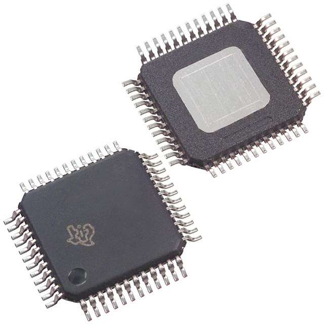
The THS1401, THS1403, and THS1408 are available in a
TQFP-48 package in standard commercial and industrial
temperature ranges. The THS1401, THS1403, and
THS1408 are also available in a PQFP-48 package in
automotive temperature range, and the THS1408 is
available in a PQFP-48 package in military temperature
range.
APPLICATIONS
D xDSL Front Ends
D Communication
D Industrial Control
D Instrumentation
D Automotive
VBG
REF+
REF
REF−
1.5 V
BG
IN+
PGA
0..7 dB
14-Bit
ADC
14
15
Buffer
D[13:0] + OV bit
IN−
6
CLK
CONTROL
LOGIC
A[1:0]
CS
WR
OE
Please be aware that an important notice concerning availability, standard warranty, and use in critical applications of Texas Instruments
semiconductor products and disclaimers thereto appears at the end of this data sheet.
All trademarks are the property of their respective owners.
Copyright 1999−2005, Texas Instruments Incorporated
��������� ���� ��!"#$%��"� �& '(##)�� %& "! *(+,�'%��"� -%�).
#"-('�&
'"�!"#$ �" &*)'�!�'%��"�& *)# �/) �)#$& "! �)0%& ��&�#($)��& &�%�-%#- 1%##%��2.
#"-('��"� *#"')&&��3 -")& �"� �)')&&%#�,2 ��',(-) �)&���3 "! %,, *%#%$)�)#&.
www.ti.com
�� *#"-('�& '"$*,�%�� �" ����
���
4 4� %,, *%#%$)�)#& %#) �)&�)- (�,)&&
"�/)#1�&) �"�)-. �� %,, "�/)# *#"-('�&� *#"-('��"� *#"')&&��3 -")& �"�
�)')&&%#�,2 ��',(-) �)&���3 "! %,, *%#%$)�)#&.
��������
������
������
www.ti.com
SLAS248D − DECEMBER 1999 − REVISED SEPTEMBER 2005
ABSOLUTE MAXIMUM RATINGS
Over operating free-air temperature range unless otherwise noted.(1)
Supply voltage, (AVDD to AGND) . . . . . . . . . . . . . . . . . . . . . . . . . . . . . . . . . . . . . . . . . . . . . . . . . . . . . . . . . . . . . 4V
Supply voltage, (DVDD to DGND) . . . . . . . . . . . . . . . . . . . . . . . . . . . . . . . . . . . . . . . . . . . . . . . . . . . . . . . . . . . . 4V
Reference input voltage range, VBG . . . . . . . . . . . . . . . . . . . . . . . . . . . . . . . . . . . . . . . − 0.3 V to AVDD + 0.3 V
Analog input voltage range . . . . . . . . . . . . . . . . . . . . . . . . . . . . . . . . . . . . . . . . . . . . . . . . . − 0.3 V to AVDD + 0.3 V
Digital input voltage range . . . . . . . . . . . . . . . . . . . . . . . . . . . . . . . . . . . . . . . . . . . . . . . . − 0.3 V to DVDD + 0.3 V
Operating free-air temperature range, TA: C-suffix . . . . . . . . . . . . . . . . . . . . . . . . . . . . . . . . . . . . . . 0°C to 70°C
I-suffix . . . . . . . . . . . . . . . . . . . . . . . . . . . . . . . . . . . . −40°C to 85°C
Q-suffix . . . . . . . . . . . . . . . . . . . . . . . . . . . . . . . . . −40°C to 125°C
M-suffix . . . . . . . . . . . . . . . . . . . . . . . . . . . . . . . . . −55°C to 125°C
Storage temperature range, Tstg . . . . . . . . . . . . . . . . . . . . . . . . . . . . . . . . . . . . . . . . . . . . . . . . . −65°C to 150°C
Lead temperature 1,6 mm (1/16 inch) from case for 10 seconds . . . . . . . . . . . . . . . . . . . . . . . . . . . . . . . 260°C
(1) Stresses beyond those listed under absolute maximum ratings may cause permanent damage to the device. These are stress ratings only, and
functional operation of the device at these or any other conditions beyond those indicated under recommended operating conditions is not implied.
Exposure to absolute-maximum-rated conditions for extended periods may affect device reliability.
Terminal Functions
TERMINAL
NAME
2
NO.
A[1:0]
40, 41
AGND
7,8, 44, 45, 46
AVDD
CLK
2, 43, 47
CML
4
32
CS
37
DGND
9, 15, 25, 33, 34
DVDD
D[13:0]
14, 20, 26, 30, 31, 42
11, 12, 13, 16, 17, 18,
19, 21, 22, 23, 24, 27,
28, 29
I/O
I
DESCRIPTION
Address input
Analog ground
Analog power supply
I
Clock input
Reference midpoint. This pin requires a 0.1-µF capacitor to AGND.
I
Chip select input. Active low.
Digital ground
Digital power supply
I/O
Data inputs/outputs
NC
38, 39
No connection; do not use. Reserved.
IN+
48
I
Positive differential analog input
IN−
1
I
Negative differential analog input
OE
35
I
Output enable. Active low.
OV
10
O
Out-of-range output
REF+
5
O
Positive reference output. This pin requires a 0.1-µF capacitor to AGND.
REF−
6
O
Negative reference output. This pin requires a 0.1-µF capacitor to AGND.
VBG
3
I
Reference input. This pin requires a 1-µF capacitor to AGND.
WR
36
I
Write signal. Active low.
��������
������
������
www.ti.com
SLAS248D − DECEMBER 1999 − REVISED SEPTEMBER 2005
NC
CS
NC
A1
A0
DV DD
AGND
AV DD
AGND
AGND
IN+
AV DD
PFB AND PHP PACKAGE
(TOP VIEW)
48 47 46 45 44 43 42 41 40 39 38 37
WR
IN−
1
36
AVDD
VBG
2
35
OE
3
34
DGND
DGND
CML
4
33
REF+
5
32
REF−
6
31
AGND
7
30
AGND
8
29
D0
D1
CLK
DVDD
DVDD
9
28
OV
10
27
D2
D13
11
26
D12
12
25
DVDD
DGND
DGND
D3
D4
D6
D5
D7
DV DD
D8
D10
D9
D11
DV DD
DGND
13 14 15 16 17 18 19 20 21 22 23 24
NC − No internal connection
AVAILABLE OPTIONS
PACKAGED DEVICE
TA
TQFP
(PFB)
PQFP (Power Pad)
(PHP)
0°C to 70°C
THS1401CPFB,
THS1403CPFB,
THS1408CPFB
—
−40°C to 85°C
THS1401IPFB,
THS1403IPFB,
THS1408IPFB
—
−40°C to 125°C
—
THS1401QPHP,
THS1403QPHP,
THS1408QPHP
−55°C to 125°C
—
THS1408MPHP
3
��������
������
������
www.ti.com
SLAS248D − DECEMBER 1999 − REVISED SEPTEMBER 2005
THERMAL CHARACTERISTICS(1)
TYP
Thermal resistance, junction-to-ambient, ΘJA
Thermal resistance, junction-to-case, ΘJC
PFB package
85.9
PHP package
28.8
PFB package
19.6
PHP package
0.79
UNIT
°C/W
°C/W
(1) Thermal resistance is modeled data, is not production tested, and is given for informational purposes only.
RECOMMENDED OPERATING CONDITIONS
MIN
NOM
MAX
Supply voltage, AVDD, DVDD
3
3.3
3.6
High level digital input, VIH
2
3.3
Low level digital input, VIL
0
Clock duty cycle
4
V
V
5
THS1401
0.1
1
1
MHz
THS1403
0.1
3
3
MHz
THS1408
0.1
8
8
MHz
C- and I-suffix
40
50
60
Q- and M-suffix
45
50
55
C-suffix
Operating free-air temperature
V
0.8
15
Load capacitance, CL
Clock frequency, fCLK
UNIT
0
25
70
I-suffix
−40
25
85
Q-suffix
−40
25
125
M-suffix
−55
25
125
pF
%
°C
��������
������
������
www.ti.com
SLAS248D − DECEMBER 1999 − REVISED SEPTEMBER 2005
ELECTRICAL CHARACTERISTICS
Over operating free-air temperature range, AVDD = DVDD = 3.3V, unless otherwise noted.
PARAMETER
TEST CONDITIONS
MIN
TYP
MAX
UNIT
81
90
mA
5
10
mA
270
360
mW
Power Supply
IDDA
IDDD
Analog supply current
Digital supply current
AVDD = 3.6 V
DVDD = 3.6 V
Power
AVDD = DVDD = 3.6 V
Power down current
µA
20
DC Characteristics
Resolution
DNL
INL
14
Integral nonlinearity
±1
THS1401
±1.5
±2.5
THS1403C/I
±1.5
±2.5
±2
±3
±3
±5
±3.5
±7.5
THS1403Q
Best fit
THS1408C/I
THS1408Q/M
Offset error
IN+ = IN−, PGA = 0 dB
C and I suffix
Gain error
Bits
±0.6
Differential nonlinearity
Q and M suffix
PGA = 0 dB
LSB
LSB
0.3
%FSR
1
%FSR
1.75
%FSR
AC Characteristics
ENOB
Effective number of bits
11.2
THS1401/3/8
THD
Total harmonic distortion
THS1403/8
THS1408
THS1401/3/8
SNR
Signal-to-noise ratio
THS1403/8
THS1408
THS1401/3/8
SINAD
Signal-to-noise ratio + distortion
THS1403/8
THS1408
THS1401/3/8
−81
fi = 4 MHz
fi = 100 kHz
−77
fi = 1 MHz
fi = 4 MHz
fi = 100 kHz
fi = 1 MHz
Spurious-free dynamic range
Analog input bandwidth
−78
THS1403Q, THS1408Q/M
fi = 1 MHz
THS1408
fi = 4 MHz
Bits
dB
72
70
72
dB
71
70
69
fi = 4 MHz
fi = 100 kHz
THS1403C/I, THS1408C/I
SFDR
11.5
fi = 100 kHz
fi = 1 MHz
70
dB
70
80
73
80
71
80
dB
80
140
MHz
5
��������
������
������
www.ti.com
SLAS248D − DECEMBER 1999 − REVISED SEPTEMBER 2005
ELECTRICAL CHARACTERISTICS (Cont.)
Over operating free-air temperature range, AVDD = DVDD = 3.3V, unless otherwise noted.
PARAMETER
TEST CONDITIONS
MIN
TYP
MAX
1.425
1.5
1.575
UNIT
Reference Voltage
Bandgap voltage, internal mode
V
Input impedance
40
kΩ
Positive reference voltage, REF+
2.5
V
Negative reference voltage, REF−
0.5
V
2
V
Reference difference, ∆REF, REF+ − REF−
Accuracy, internal reference
5%
Temperature coefficient
Voltage coefficient
40
ppm/°C
200
ppm/V
Analog Inputs
Positive analog input, IN+
0
Negative analog input, IN−
Analog input voltage difference
∆AIN = IN+ − IN−, VREF = REF+ − REF−
V
0
AVDD
AVDD
−VREF
VREF
V
Input impedance
25
PGA range
0
PGA step size
kΩ
7
1
dB
dB
±0.25
PGA gain error
V
dB
Digital Inputs
VIH
VIL
High-level digital input
2
V
Low-level digital input
0.8
Input capacitance
5
±1
Input current
V
pF
µA
Digital Outputs
VOH
VOL
High-level digital output
Low-level digital output
IOH = 50 µA
IOL = 50 µA
2.6
V
IOZ
Output current, high impedance
Clock Timing (CS low)
td
Clock frequency
1
1
MHz
THS1403
3
3
MHz
THS1408
0.1†
8
8
MHz
Output delay time
Latency
† This parameter is not production tested for Q- and M-suffix devices.
6
V
µA
0.1†
0.1†
THS1401
fCLK
0.4
±10
25
9.5
ns
Cycles
��������
������
������
www.ti.com
SLAS248D − DECEMBER 1999 − REVISED SEPTEMBER 2005
PARAMETER MEASUREMENT INFORMATION
sample timing
The THS1401/3/8 core is based on a pipeline architecture with a latency of 9.5 samples. The conversion results
appear on the digital output 9.5 clock cycles after the input signal was sampled.
S11
S9
S12
S10
Analog
Input
tw(CLK)
tw(CLK)
CLK
td
Data
Out
C1
C2
C3
Figure 1. Sample Timing
The parallel interface of the THS1401/3/8 ADC features 3-state buffers, making it possible to directly connect
it to a data bus. The output buffers are enabled by driving the OE input low.
Besides the sample results, it is also possible to read back the values of the control register, the PGA register,
and the offset register. Which register is read is determined by the address inputs A[1,0]. The ADC results are
available at address 0.
The timing of the control signals is described in the following sections.
7
��������
������
������
www.ti.com
SLAS248D − DECEMBER 1999 − REVISED SEPTEMBER 2005
PARAMETER MEASUREMENT INFORMATION
read timing (15-pF load)
PARAMETER
tsu(OE−ACS)
ten
Address and chip select setup time
tdis
th(A)
Output disable
MIN
TYP
MAX
4
ns
Output enable
15
10
Address hold time
th(CS)
Chip select hold time
NOTE: All timing parameters refer to a 50% level.
ns
ns
0
ns
th(CS)
OE
ten
tdis
DATA
D[13:0]
OV
th(A)
A[1:0]
X
ADDRESS
Figure 2. Read Timing
8
ns
1
CS
tsu(OE−ACS)
UNIT
X
��������
������
������
www.ti.com
SLAS248D − DECEMBER 1999 − REVISED SEPTEMBER 2005
PARAMETER MEASUREMENT INFORMATION
write timing (15-pF load)
PARAMETER
tsu(WE−CS)
tsu(DA)
Chip select setup time
th(DA)
th(CS)
MIN
TYP
MAX
UNIT
4
ns
Data and address setup time
29
ns
Data and address hold time
0
ns
Chip select hold time
0
ns
15
ns
twH(WE)
Write pulse duration high
NOTE: All timing parameters refer to a 50% level.
CS
th(CS)
WE
tsu(WE−CS)
D[13:0]
tsu(DA)
X
DATA
X
th(DA)
A
X
ADDRESS
X
Figure 3. Write Timing
9
��������
������
������
www.ti.com
SLAS248D − DECEMBER 1999 − REVISED SEPTEMBER 2005
TYPICAL CHARACTERISTICS
POWER
vs
FREQUENCY
SUPPLY CURRENT
vs
TIME
284
90
282
80
70
I CC − Supply Current − mA
Power − mW
280
278
276
274
272
270
60
50
40
30
20
10
0
268
0.1
1
f − Frequency − MHz
10
0
50
Figure 4
100
150
200
t − Time − ns
250
Figure 5
FAST FOURIER TRANSFORM
0
fs = 1 MSPS,
fI = 100 kHz,
−1 dB
Output − dB
−20
−40
−60
−80
−100
−120
−140
0
100
200
300
f − Frequency − kHz
Figure 6
10
400
500
300
��������
������
������
www.ti.com
SLAS248D − DECEMBER 1999 − REVISED SEPTEMBER 2005
TYPICAL CHARACTERISTICS
FAST FOURIER TRANSFORM
0
fs = 3 MSPS,
fI = 1 MHz,
−1 dB
Output − dB
−20
−40
−60
−80
−100
−120
−140
0.1
0.4
0.7
1.3
1
f − Frequency − MHz
Figure 7
FAST FOURIER TRANSFORM
0
fs = 8 MSPS,
fI = 1 MHz,
−1 dB
Output − dB
−20
−40
−60
−80
−100
−120
−140
0.1
0.4
0.7
1
1.3
1.6
1.9
2.2
2.5
2.8
3.1
3.4
3.7
4
f − Frequency − MHz
Figure 8
INL − Integral Nonlinearity − LSB
INTEGRAL NONLINEARITY
2
fs = 1 MSPS
1.5
1
0.5
0
−0.5
−1
−1.5
−2
0
2048
4096
6144
8192
10240
12288
14336
16384
Samples
Figure 9
11
��������
������
������
www.ti.com
SLAS248D − DECEMBER 1999 − REVISED SEPTEMBER 2005
TYPICAL CHARACTERISTICS
INL − Integral Nonlinearity − LSB
INTEGRAL NONLINEARITY
2
fs = 3 MSPS
1.5
1
0.5
0
−0.5
−1
−1.5
−2
0
2048
4096
6144
8192
10240
12288
14336
16384
Samples
Figure 10
INL − Integral Nonlinearity − LSB
INTEGRAL NONLINEARITY
4
fs = 8 MSPS
3
2
1
0
−1
−2
−3
−4
0
2048
4096
6144
8192
10240
12288
14336
16384
Samples
Figure 11
DNL − Differential Nonlinearity − LSB
DIFFERENTIAL NONLINEARITY
1
0.8
0.6
fs = 1 MSPS
0.4
0.2
0
−0.2
−0.4
−0.6
−0.8
−1
0
2048
4096
6144
8192
Samples
Figure 12
12
10240
12288
14336
16384
��������
������
������
www.ti.com
SLAS248D − DECEMBER 1999 − REVISED SEPTEMBER 2005
TYPICAL CHARACTERISTICS
DNL − Differential Nonlinearity − LSB
DIFFERENTIAL NONLINEARITY
1
0.8
fs = 3 MSPS
0.6
0.4
0.2
0
−0.2
−0.4
−0.6
−0.8
−1
0
2048
4096
6144
8192
10240
12288
14336
16384
Samples
Figure 13
DNL − Differential Nonlinearity − LSB
DIFFERENTIAL NONLINEARITY
1
0.8
0.6
fs = 8 MSPS
0.4
0.2
0
−0.2
−0.4
−0.6
−0.8
−1
0
2048
4096
6144
8192
10240
12288
14336
16384
Samples
Figure 14
13
��������
������
������
www.ti.com
SLAS248D − DECEMBER 1999 − REVISED SEPTEMBER 2005
TYPICAL CHARACTERISTICS
TOTAL HARMONIC DISTORTION
vs
FREQUENCY
TOTAL HARMONIC DISTORTION
vs
FREQUENCY
−70
−70
fs = 8 MSPS,
fI at −1 dB
−72
THD − Total Harmonic Distortion − dB
THD − Total Harmonic Distortion − dB
−72
fs = 3 MSPS,
fI at −1 dB
−74
−76
−78
−80
−82
−84
−86
−88
−74
−76
−78
−80
−82
−84
−86
−88
−90
10
−90
100
f − Frequency − Hz
1000 1500
10
100
Figure 16
SIGNAL-TO-NOISE RATIO
vs
FREQUENCY
SIGNAL-TO-NOISE RATIO
vs
FREQUENCY
80
78
SNR − Signal-to-Noise Ratio − dB
SNR − Signal-to-Noise Ratio − dB
80
fs = 3 MSPS,
fI at −1 dB
76
74
72
70
68
66
64
62
60
10
fs = 8 MSPS,
fI at −1 dB
76
74
72
70
68
66
64
62
100
f − Frequency − Hz
Figure 17
14
4000
f − Frequency − Hz
Figure 15
78
1000
1000 1500
60
10
100
f − Frequency − Hz
Figure 18
1000
4000
��������
������
������
www.ti.com
SLAS248D − DECEMBER 1999 − REVISED SEPTEMBER 2005
PRINCIPLES OF OPERATION
registers
The device contains several registers. The A register is selected by the values of bits A1 and A0:
A1
A0
Register
0
0
Conversion result
0
1
PGA
1
0
Offset
1
1
Control
Tables 1 and 2 describe how to read the conversion results and how to configure the data converter. The default
values (were applicable) show the state after a power-on reset.
Table 1. Conversion Result Register, Address 0, Read
BIT
D13
D12
D11
D10
D9
D8
D7
D6
D5
D4
D3
D2
D1
D0
Function
MSB
...
…
…
…
…
…
…
…
…
…
…
…
LSB
The output can be configured for 2s complement or straight binary format (see D11/control register).
The output code is given by:
2s complement:
−8192 at ∆IN = −∆REF
0
at ∆IN = 0
8191 ∆IN = +∆REF − 1 LSB
Straight binary:
0
at ∆IN = −∆REF
8192 at ∆IN = 0
16383 at ∆IN = + ∆REF − 1 LSB
1 LSB + 2DREF
16384
Table 2. PGA Gain Register, Address 1, Read/Write
BIT
D13
D12
D11
D10
D9
D8
D7
D6
D5
D4
D3
D2
D1
D0
Function
X
X
X
X
X
X
X
X
X
X
X
G2
G1
G0
Default
0
0
0
0
0
0
0
0
0
0
0
0
0
0
The PGA gain is determined by writing to G2−0.
Gain (dB) = 1dB × G2−0. max = 7dB. The range of G2−0 is 0 to 7.
Table 3. Offset Register, Address 2, Read/Write
BIT
D13
D12
D11
D10
D9
D8
D7
D6
D5
D4
D3
D2
D1
D0
Function
X
X
X
X
X
X
MSB
…
…
…
…
…
…
LSB
Default
0
0
0
0
0
0
0
0
0
0
0
0
0
0
The offset correction range is from –128 to 127 LSB. This value is added to the conversion results from the ADC.
15
��������
������
������
www.ti.com
SLAS248D − DECEMBER 1999 − REVISED SEPTEMBER 2005
PRINCIPLES OF OPERATION
Table 4. Control Register, Address 3, Read
BIT
D13
D12
D11
D10
D9
D8
D7
D6
D5
D4
D3
D2
D1
D0
Function
PWD
REF
FOR
TM2
TM1
TM0
OFF
RES
RES
RES
RES
RES
RES
RES
Table 5. Control Register, Address 3, Write
BIT
D13
D12
D11
D10
D9
D8
D7
D6
D5
D4
D3
D2
D1
D0
Function
PWD
REF
FOR
TM2
TM1
TM0
OFF
RES
RES
RES
RES
RES
RES
RES
Default
0
0
0
0
0
0
0
0
0
0
0
0
0
0
PWD:
Power down
0 = normal operation
1 = power down
REF:
Reference select
0 = internal reference
1 = external reference
FOR:
Output format
0 = straight binary
1 = 2s complement
TM2−0:
Test mode
000 = normal operation
001 = both inputs = REF−
010 = IN+ at VCM (Voltage at CML pin), IN− at REF−
011 = IN+ at REF+, IN− at REF−
100 = normal operation
101 = both inputs = REF+
110 = IN+ at REF−, IN− at VCM (Voltage at CML pin)
111 = IN+ at REF−, IN− at REF+
OF:
Offset correction
0 = enable
1 = disable
RES
Reserved
Must be set to 0.
APPLICATION INFORMATION
driving the analog input
The THS1401/3/8 ADCs have a fully differential input. A differential input is advantageous with respect to SNR,
SFDR, and THD performance because the signal peak-to-peak level is 50% of a comparable single-ended
input.
There are three basic input configurations:
D Fully differential
D Transformer coupled single-ended to differential
D Single-ended
fully differential configuration
In this configuration, the ADC converts the difference (∆IN) of the two input signals on IN+ and IN−.
22 Ω
100 pF
IN+
THS1401/3/8
22 Ω
IN−
100 pF
Figure 19. Differential Input
16
��������
������
������
www.ti.com
SLAS248D − DECEMBER 1999 − REVISED SEPTEMBER 2005
The resistors and capacitors on the inputs decouple the driving source output from the ADC input and also serve
as first order low pass filters to attenuate out of band noise.
The input range on both inputs is 0 V to AVDD. The full-scale value is determined by the voltage reference. The
positive full-scale output is reached, if ∆IN equals ∆REF, the negative full-scale output is reached, if ∆IN equals
−∆REF.
∆IN [V]
OUTPUT
−∆REF
− full scale
0
0
∆REF
+ full scale
APPLICATION INFORMATION
transformer coupled single-ended to differential configuration
If the application requires the best SNR, SFDR, and THD performance, the input should be transformer
coupled.
The signal amplitude on both inputs of the ADC is one half as high as in a single-ended configuration thus
increasing the ADC ac performance.
22 Ω
IN+
100 pF
R
THS1401/3/8
22 Ω
IN−
100 pF
+
CML
1 µF
0.1 µF
Figure 20. Transformer Coupled
The following table shows the input voltages for negative full-scale output, zero output, and positive full-scale
output:
IN [VPEAK]
−∆REF
OUTPUT [PEAK]
− full scale†
0
0
∆REF
+ full scale†
† n = 1 (winding ratio)
The resistor R of the transformer coupled input configuration must be set to match the signal source impedance
R = n2 Rs, where Rs is the source impedance and n is the transformer winding ratio.
APPLICATION INFORMATION
single-ended configuration
In this configuration, the input signal is level shifted by ∆REF/2.
17
��������
������
������
www.ti.com
SLAS248D − DECEMBER 1999 − REVISED SEPTEMBER 2005
10 kΩ + 10 kΩ
10 kΩ
10 kΩ
IN+
100 pF
REF+
THS1401/3/8
22 Ω
−
IN−
100 pF
+
10 kΩ
REF−
10 kΩ
Figure 21. Single-Ended With Level Shift
The following table shows the input voltages for negative full-scale output, zero output, and positive full-scale
output:
∆IN+ [V]
OUTPUT
−∆REF
− full scale
0
0
∆REF
+ full scale
Note that the resistors of the op-amp and the op-amp all introduce gain and offset errors. Those errors can be
trimmed by varying the values of the resistors.
Because of the added offset, the op-amp does not necessarily operate in the best region of its transfer curve
(best linearity around zero) and therefore may introduce unacceptable distortion. For ac signals, an alternative
is described in the following section.
APPLICATION INFORMATION
AC-coupled single-ended configuration
If the application does not require the signal bandwidth to include dc, the level shift shown in Figure 21 is not
necessary.
10 kΩ
10 kΩ
10 kΩ
10 kΩ
IN+
100 pF
REF+
THS1401/3/8
−
+
10 nF
IN−
22 Ω
100 pF
REF−
10 kΩ
10 kΩ
Figure 22. Single-Ended With Level Shift
Because the signal swing on the op-amp is centered around ground, it is more likely that the signal stays within
the linear region of the op-amp transfer function, thus increasing the overall ac performance.
IN [VPEAK]
OUTPUT [PEAK]
−∆REF
− full scale
0
0
∆REF
+ full scale
Compared to the transformer-coupled configuration, the swing on IN− is twice as big, which can decrease the
ac performance (SNR, SFD, and THD).
18
��������
������
������
www.ti.com
SLAS248D − DECEMBER 1999 − REVISED SEPTEMBER 2005
APPLICATION INFORMATION
internal/external reference operation
The THS1401/3/8 ADC can either be operated
using the built-in band gap reference or using an
external precision reference in case very high dc
accuracy is needed.
The REF+ and REF+ outputs are given by:
ǒ
Ǔ
REF )+ VBG 1 ) 2 and REF–
3
If the built-in reference is used, VBG equals 1.5 V
which results in REF+ = 2.5 V, REF− = 0.5 V and
∆REF = 2 V.
The internal reference can be disabled by writing
1 to D12 (REF) in the control register (address 3).
The band gap reference is then disconnected and
can be substituted by a voltage on the VBG pin.
programmable gain amplifier
The on-chip programmable gain amplifier (PGA)
has eight gain settings. The gain can be changed
by writing to the PGA gain register (address 1).
The range is 0 to 7dB in steps of one dB.
out of range indication
The OV output of the ADC indicates an out of
range condition. Every time the difference on the
analog inputs exceeds the differential reference,
this signal is asserted. This signal is updated the
same way as the digital data outputs and therefore
subject to the same pipeline delay.
conditioning circuitry. If the offset compensation is
enabled (D7 (OFF) in the control register), the
value in the offset register (address 2) is
automatically added to the output of the ADC.
In order to set the correct value of the offset
compensation register, the ADC result when the
input signal is 0 must be read by the host
processor and written to the offset register
(address 2).
test modes
The ADC core operation can be tested by
selecting one of the available test modes (see
control register description). The test modes
apply various voltages to the differential input
depending on the setting in the control register.
digital I/O
The digital inputs and outputs of the THS1401/3/8
ADC are 3-V CMOS compatible. In order to avoid
current feed back errors, the capacitive load on
the digital outputs should be as low as possible (50
pF max). Series resistors (100 Ω) on the digital
outputs can improve the performance by limiting
the current during output transitions.
The parallel interface of the THS1401/3/8 ADC
features 3-state buffers, making it possible to
directly connect it to a data bus. The output buffers
are enabled by driving the OE input low.
Refer to the read and write timing diagrams in the
parameter measurement information section for
information on read and write access.
offset compensation
With the offset register it is possible to
automatically compensate system offset errors,
including errors caused by additional signal
19
��������
������
������
www.ti.com
SLAS248D − DECEMBER 1999 − REVISED SEPTEMBER 2005
Revision History
DATE
9/05
REV
D
PAGE
SECTION
1
—
Updated page 1 format and layout.
1
—
Moved funtional block diagram from page 2.
2
—
Moved Terminal Function table from page 3.
2
—
Moved Absolute Maximum table from page 4.
3
—
Moved package pinout from page 1.
3
—
Moved Ordering Options table from page 2.
15
16
DESCRIPTION
Principles of Operation
Table 1. In section 2s complement: 8191 DIN = − DREF − 1 LSB changed to
8191 DIN = +DREF − 1 LSB. In section Straight Binary: 16383 at DIN = − DREF
− 1 LSB should be changed to 16383 DIN = +DREF − 1 LSB
Principles of Operation
Table 5. In section TM2−0: Test Mode: 010 = IN+ at VREF /2, IN− at REF−,
changed to, 010 = IN+ at VCM (Voltage at CML pin), IN− at REF−. Same section:
110 = IN+ at REF−, IN− at VREF /2, changed to, 110 = IN+ at REF−, IN− at VCM
(Voltage at CML pin)
NOTE: Page numbers for previous revisions may differ from page numbers in the current version.
20
�PACKAGE OPTION ADDENDUM
www.ti.com
10-Dec-2020
PACKAGING INFORMATION
Orderable Device
Status
(1)
Package Type Package Pins Package
Drawing
Qty
Eco Plan
(2)
Lead finish/
Ball material
MSL Peak Temp
Op Temp (°C)
Device Marking
(3)
(4/5)
(6)
5962-0051101NXD
ACTIVE
HTQFP
PHP
48
250
RoHS & Green
NIPDAU
Level-3-260C-168 HR
-55 to 125
0051101
NXD
THS1401IPFB
ACTIVE
TQFP
PFB
48
250
RoHS & Green
NIPDAU
Level-2-260C-1 YEAR
-40 to 85
TJ1401
THS1403IPFB
ACTIVE
TQFP
PFB
48
250
RoHS & Green
NIPDAU
Level-2-260C-1 YEAR
-40 to 85
TJ1403
THS1408IPFB
ACTIVE
TQFP
PFB
48
250
RoHS & Green
NIPDAU
Level-2-260C-1 YEAR
-40 to 85
TJ1408
(1)
The marketing status values are defined as follows:
ACTIVE: Product device recommended for new designs.
LIFEBUY: TI has announced that the device will be discontinued, and a lifetime-buy period is in effect.
NRND: Not recommended for new designs. Device is in production to support existing customers, but TI does not recommend using this part in a new design.
PREVIEW: Device has been announced but is not in production. Samples may or may not be available.
OBSOLETE: TI has discontinued the production of the device.
(2)
RoHS: TI defines "RoHS" to mean semiconductor products that are compliant with the current EU RoHS requirements for all 10 RoHS substances, including the requirement that RoHS substance
do not exceed 0.1% by weight in homogeneous materials. Where designed to be soldered at high temperatures, "RoHS" products are suitable for use in specified lead-free processes. TI may
reference these types of products as "Pb-Free".
RoHS Exempt: TI defines "RoHS Exempt" to mean products that contain lead but are compliant with EU RoHS pursuant to a specific EU RoHS exemption.
Green: TI defines "Green" to mean the content of Chlorine (Cl) and Bromine (Br) based flame retardants meet JS709B low halogen requirements of