Product
Folder
Order
Now
Support &
Community
Tools &
Software
Technical
Documents
Reference
Design
THS4531A
SLOS823D – DECEMBER 2012 – REVISED MARCH 2020
THS4531A Ultra Low-Power, Rail-to-Rail Output, Fully Differential Amplifier
1 Features
3 Description
•
The THS4531A device is a low-power, fully
differential amplifier with input common-mode range
below the negative rail and rail-to-rail output. The
device is designed for low-power data acquisition
systems and high-density applications where power
consumption and dissipation is critical.
•
•
•
•
•
•
•
•
•
•
•
Ultra Low-Power:
– Voltage: 2.5 V to 5.5 V
– Current: 250 µA
– Power-Down Mode: 0.5 µA (Typical)
Fully Differential Architecture
Bandwidth: 36 MHz (Av = 1 V/V)
Slew Rate: 200 V/µs
THD: –120 dBc at 1 kHz (1 VRMS, RL= 2 kΩ)
Input Voltage Noise: 10 nV/√Hz (f = 1 kHz)
High DC Accuracy:
– VOS: ±100 µV
– VOS Drift: ±3 µV/˚C (–40°C to +125°C)
– AOL: 114 dB
Rail-to-Rail Output (RRO)
Negative Rail Input (NRI)
Output Common-Mode Control
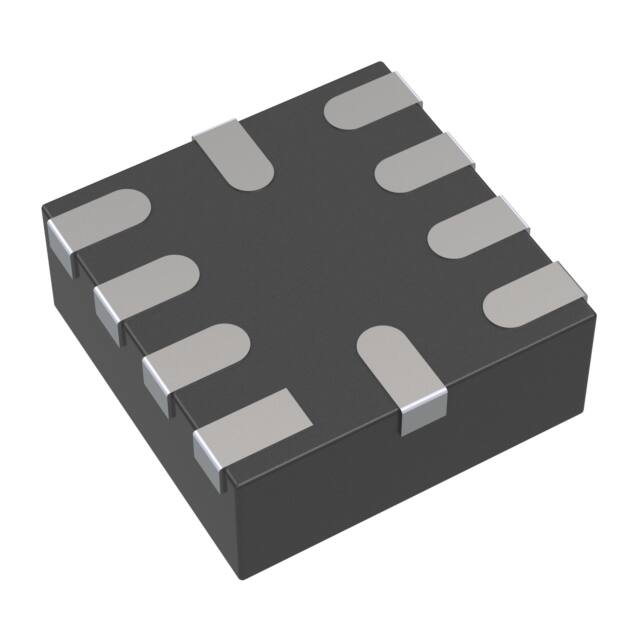
8-Pin SOIC (D) and VSSOP (DGK)
10-Pin WQFN (RUN)
2 Applications
•
•
•
•
•
Low-Power SAR, ΔΣ ADC Driver
Low-Power, High Performance:
– Differential-to-Differential Amplifier
– Single-Ended to Differential Amplifier
Low-Power, Wide-Bandwidth Differential Driver
Low-Power, Wide-Bandwidth Differential Signal
Conditioning
High-Channel Count and Power Dense Systems
The device features accurate output common-mode
control that allows for DC coupling when driving
analog-to-digital converters (ADCs). This control,
coupled with the input common-mode range below
the negative rail and rail-to-rail output, allows for easy
interface from single-ended ground-referenced signal
sources to successive-approximation registers
(SARs), and delta-sigma (ΔΣ) ADCs using only
single-supply 2.5-V to 5-V power. The THS4531A is
also a valuable tool for general-purpose, low-power
differential signal conditioning applications.
Device Information(1)
PART NUMBER
THS4531A
PACKAGE
BODY SIZE (NOM)
SOIC (8)
4.90 mm × 3.91 mm
VSSOP (8)
3.00 mm × 3.00 mm
WQFN (10)
2.00 mm × 2.00 mm
(1) For all available packages, see the orderable addendum at
the end of the data sheet.
1-kHz FFT Plot on Audio Analyzer
Magnitude (dBV)
1
0
−10
−20
−30
−40
−50
−60
−70
−80
−90
−100
−110
−120
−130
−140
VS = 5 V
G = 1 V/V
VOUT = 1 VRMS
RF = 2 kΩ
RL = 600 Ω
0
5k
10k
15k
Frequency (Hz)
20k
24k
G071
1
An IMPORTANT NOTICE at the end of this data sheet addresses availability, warranty, changes, use in safety-critical applications,
intellectual property matters and other important disclaimers. PRODUCTION DATA.
�THS4531A
SLOS823D – DECEMBER 2012 – REVISED MARCH 2020
www.ti.com
Table of Contents
1
2
3
4
5
6
7
Features ..................................................................
Applications ...........................................................
Description .............................................................
Revision History.....................................................
Related Products ...................................................
Pin Configuration and Functions .........................
Specifications.........................................................
7.1
7.2
7.3
7.4
7.5
7.6
7.7
8
1
1
1
2
3
4
5
Absolute Maximum Ratings ...................................... 5
ESD Ratings.............................................................. 5
Recommended Operating Conditions....................... 5
Thermal Information .................................................. 5
Electrical Characteristics: VS = 2.7 V........................ 6
Electrical Characteristics: VS = 5 V........................... 8
Typical Characteristics ............................................ 11
Detailed Description ............................................ 24
8.1 Overview ................................................................. 24
8.2 Functional Block Diagram ....................................... 24
8.3 Feature Description................................................. 24
8.4 Device Functional Modes........................................ 26
9
Application and Implementation ........................ 27
9.1 Application Information............................................ 27
9.2 Typical Applications ................................................ 35
10 Power Supply Recommendations ..................... 45
11 Layout................................................................... 45
11.1 Layout Guidelines ................................................. 45
11.2 Layout Example .................................................... 46
12 Device and Documentation Support ................. 47
12.1
12.2
12.3
12.4
12.5
12.6
Device Support......................................................
Documentation Support ........................................
Community Resources..........................................
Trademarks ...........................................................
Electrostatic Discharge Caution ............................
Glossary ................................................................
47
47
48
48
48
48
13 Mechanical, Packaging, and Orderable
Information ........................................................... 48
4 Revision History
NOTE: Page numbers for previous revisions may differ from page numbers in the current version.
Changes from Revision C (January 2016) to Revision D
•
Changed maximum range of the continuous input current, Ii From: 0.75 mA To: 10 mA ...................................................... 5
Changes from Revision B (June 2015) to Revision C
•
2
Page
Added Pin Configuration and Functions section, ESD Ratings table, Feature Description section, Device Functional
Modes, Application and Implementation section, Power Supply Recommendations section, Layout section, Device
and Documentation Support section, and Mechanical, Packaging, and Orderable Information section .............................. 1
Changes from Original (December 2012) to Revision A
•
Page
Changed Equation 5 for clarification ................................................................................................................................... 40
Changes from Revision A (January 2013) to Revision B
•
Page
Page
Changed graph title from "VOS OVER TEMPERATURE" to "SMALL-SIGNAL FREQUENCY RESPONSE" ...................... 18
Submit Documentation Feedback
Copyright © 2012–2020, Texas Instruments Incorporated
Product Folder Links: THS4531A
�THS4531A
www.ti.com
SLOS823D – DECEMBER 2012 – REVISED MARCH 2020
5 Related Products
Table 1. Related Amplifiers
DEVICE
BW (MHz)
IQ (mA)
THD (dBc) at
100 kHz
VN (nV/√Hz)
RAIL-TO-RAIL
DUAL PART
NUMBERS
THS4531A
36
0.25
–104
10
Negative In, Out
THS4532
THS4121
100
16
–79
5.4
Out
THS4521
145
1.14
–120
4.6
Negative In, Out
THS4131
150
16
–107
1.3
No
THS4520
620
14.2
–107
2
Out
THS4541
850
10.1
–137
2.2
Negative In, Out
THS4522
Table 2. Related Precision ADCs
DEVICE
BITS
MAX DATA RATE
(kSPS)
NOMINAL SUPPLY
(V)
NOMINAL ICC (mA)
MAX CLK RATE
TYPICAL POWER (mW)
MAX CLK RATE
ADS8881
18
1000
ADS8861
16
1000
5
1.1
5.5
3.3
1.67
ADS8321E
16
100
5
0.9
5.3
4.5
ADS7945
14
2000
5
2.32
5.8/ch (dual)
ADS7044
12
1000
3
0.3
0.9
Submit Documentation Feedback
Copyright © 2012–2020, Texas Instruments Incorporated
Product Folder Links: THS4531A
3
�THS4531A
SLOS823D – DECEMBER 2012 – REVISED MARCH 2020
www.ti.com
6 Pin Configuration and Functions
D and DGK Packages
8-Pin SOIC and VSSOP
Top View
RUN Package
10-Pin WQFN
Top View
VS+
VIN-
1
8
VIN+
VOCM
2
7
PD
VOUT-
1
9
VOUT+
VS+
3
6
VS-
NC
2
8
NC
VOUT+
4
5
VOUT-
PD
3
7
VOCM
VIN+
4
6
VIN-
10
5
VS-
Pin Functions
PIN
NAME
SOIC,
VSSOP
WQFN
2
I/O
NC
—
PD
7
3
I
Power-down, PD = logic low = low power mode, PD = logic high = normal operation (PIN
MUST BE DRIVEN)
VIN+
8
4
I
Non-inverted amplifier input
VIN–
1
6
I
Inverting amplifier input
VOCM
2
7
I
Common-mode voltage input
VOUT+
4
9
O
Non-inverted amplifier output
VOUT–
5
1
O
Inverted amplifier output
VS+
3
10
I
Amplifier positive power-supply input
VS–
6
5
I
Amplifier negative power-supply input. On multichannel devices, VS– is tied together.
4
8
—
DESCRIPTION
No internal connection
Submit Documentation Feedback
Copyright © 2012–2020, Texas Instruments Incorporated
Product Folder Links: THS4531A
�THS4531A
www.ti.com
SLOS823D – DECEMBER 2012 – REVISED MARCH 2020
7 Specifications
7.1 Absolute Maximum Ratings
MIN
MAX
Supply voltage, VS– to VS+
UNIT
5.5
Input/output voltage, VIN±, VOUT±, and VOCM pins
(VS+) + 0.7
V
Differential input voltage, VID
(VS–) – 0.7
1
V
Continuous output current, IO
50
mA
Continuous input current, Ii
10
mA
Continuous power dissipation
See Thermal Information
Maximum junction temperature, TJ
150
°C
Operating free-air temperature, TA
–40
125
°C
Storage temperature, Tstg
–65
150
°C
VALUE
UNIT
7.2 ESD Ratings
V(ESD)
(1)
(2)
Electrostatic discharge
Human-body model (HBM), per ANSI/ESDA/JEDEC JS-001 (1)
±3000
Charged-device model (CDM), per JEDEC specification JESD22C101 (2)
±500
V
JEDEC document JEP155 states that 500-V HBM allows safe manufacturing with a standard ESD control process.
JEDEC document JEP157 states that 250-V CDM allows safe manufacturing with a standard ESD control process.
7.3 Recommended Operating Conditions
Over operating free-air temperature range (unless otherwise noted).
MIN
NOM
MAX
VS+
Single-supply voltage
2.7
5
5.4
UNIT
V
TA
Ambient temperature
–40
25
125
°C
7.4 Thermal Information
THS4531A
THERMAL METRIC (1)
RθJA
DGK (VSSOP)
RUN (WQFN)
8 PINS
8 PINS
10 PINS
UNIT
133
198
163
°C/W
RθJC(top) Junction-to-case (top) thermal resistance
78
84
66
°C/W
RθJB
Junction-to-board thermal resistance
73
120
113
°C/W
ψJT
Junction-to-top characterization parameter
26
19
17
°C/W
ψJB
Junction-to-board characterization parameter
73
118
113
°C/W
RθJC(bot) Junction-to-case (bottom) thermal resistance
N/A
N/A
N/A
°C/W
(1)
Junction-to-ambient thermal resistance
D (SOIC)
For more information about traditional and new thermal metrics, see the Semiconductor and IC Package Thermal Metrics application
report, SPRA953.
Submit Documentation Feedback
Copyright © 2012–2020, Texas Instruments Incorporated
Product Folder Links: THS4531A
5
�THS4531A
SLOS823D – DECEMBER 2012 – REVISED MARCH 2020
www.ti.com
7.5 Electrical Characteristics: VS = 2.7 V
Test conditions at TA ≈ 25°C, VS+ = 2.7 V, VS– = 0 V, VOCM = open, VOUT = 2 VPP, RF = 2 kΩ, RL = 2 kΩ differential, G = 1 V/V,
single-ended input, differential output, and output referenced to mid-supply, unless otherwise noted.
PARAMETER
TEST CONDITIONS
MIN
TYP
MAX
UNIT
TEST
LEVEL
MHz
C
AC PERFORMANCE
Small-signal bandwidth
VOUT = 100 mVPP, G = 1
34
VOUT = 100 mVPP, G = 2
16
VOUT = 100 mVPP, G = 5
6
VOUT = 100 mVPP, G = 10
2.7
Gain-bandwidth product
VOUT = 100 mVPP, G = 10
27
MHz
C
Large-signal bandwidth
VOUT = 2 VPP, G = 1
34
MHz
C
Bandwidth for 0.1-dB flatness
VOUT = 2 VPP, G = 1
12
MHz
C
Slew rate, rise/fall, 25% to 75%
VOUT = 2-V step
190/320
V/µs
C
Rise/fall time, 10% to 90%
VOUT = 2-V step
6
ns
C
Settling time to 1%
VOUT = 2-V step
25
ns
C
Settling time to 0.1%
VOUT = 2-V step
60
ns
C
Settling time to 0.01%
VOUT = 2-V step
150
ns
C
Overshoot/undershoot
VOUT = 2-V step
2nd-order harmonic distortion
1%
f = 1 kHz, VOUT = 2 VPP
–122
f = 10 kHz
–127
f = 1 MHz
C
dBc
C
dBc
C
–59
f = 1 kHz, VOUT = 2 VPP
–136
f = 10 kHz
–135
f = 1 MHz
–70
2nd-order intermodulation distortion
f = 1 MHz, 200-kHz tone spacing,
VOUT = 1 Vpp each tone
–83
dBc
C
3rd-order intermodulation distortion
f = 1 MHz, 200-kHz tone spacing,
VOUT = 1 Vpp each tone
–81
dBc
C
Input voltage noise
f = 1 kHz
10
nV/√Hz
C
3rd-order harmonic distortion
Voltage noise 1/f corner frequency
Input current noise
45
f = 100 kHz
Current noise 1/f corner frequency
Hz
C
0.25
pA/√Hz
C
6.5
kHz
C
Overdrive recovery time
Overdrive = 0.5 V
65
ns
C
Output balance error
VOUT = 100 mV, f = 1 MHz
–65
dB
C
Closed-loop output impedance
f = 1 MHz (differential)
2.5
Ω
C
dB
A
DC PERFORMANCE
Open-loop voltage gain (AOL)
Input-referred offset voltage
Input offset voltage drift
(1)
6
(1)
100
113
TA = 25°C
–400
±100
TA = 0°C to +70°C
–715
715
TA = –40°C to +85°C
–855
855
TA = –40°C to +125°C
–1300
1300
400
TA = 0°C to 70°C
–7
±2
7
TA = –40°C to +85°C
–7
±2
7
TA = –40°C to +125°C
–9
±3
9
A
µV
µV/°C
B
B
Input offset voltage drift, input bias current drift, and input offset current drift are average values calculated by taking data at the end
points, computing the difference, and dividing by the temperature range.
Submit Documentation Feedback
Copyright © 2012–2020, Texas Instruments Incorporated
Product Folder Links: THS4531A
�THS4531A
www.ti.com
SLOS823D – DECEMBER 2012 – REVISED MARCH 2020
Electrical Characteristics: VS = 2.7 V (continued)
Test conditions at TA ≈ 25°C, VS+ = 2.7 V, VS– = 0 V, VOCM = open, VOUT = 2 VPP, RF = 2 kΩ, RL = 2 kΩ differential, G = 1 V/V,
single-ended input, differential output, and output referenced to mid-supply, unless otherwise noted.
PARAMETER
TEST CONDITIONS
MIN
TA = 25°C
Input bias current (2)
TYP
MAX
200
250
TA = 0°C to +70°C
275
TA = –40°C to +85°C
286
TA = –40°C to +125°C
Input bias current drift (1)
Input offset current drift (1)
TEST
LEVEL
A
nA
B
305
TA = 0°C to +70°C
0.45
0.55
TA = –40°C to +85°C
0.45
0.55
0.45
0.55
±5
50
TA = –40°C to +125°C
Input offset current
UNIT
TA = 25°C
–50
TA = 0°C to +70°C
–55
55
TA = –40°C to +85°C
–57
57
TA = –40°C to +125°C
–60
60
TA = 0°C to +70°C
–0.1
±0.03
0.1
TA = –40°C to +85°C
–0.1
±0.03
0.1
TA = –40°C to +125°C
–0.1
±0.03
0.1
VS– – 0.2
VS–
VS– – 0.2
VS–
nA/°C
B
A
nA
nA/°C
B
B
INPUT
Common-mode input low
Common-mode input high
TA = 25°C, CMRR > 87 dB
TA = –40°C to +125°C, CMRR > 87 dB
TA = 25°C, CMRR > 87 dB
VS+ – 1.2 VS+ – 1.1
TA = –40°C to +125°C, CMRR > 87 dB
VS+ – 1.2 VS+ – 1.1
Common-mode rejection ratio
90
Input impedance differential mode
V
V
116
200 || 1
A
B
A
B
dB
A
kΩ || pF
C
OUTPUT
TA = 25°C
Single-ended output voltage: low
TA = –40°C to +125°C
TA = 25°C
VS+ – 0.2
Single-ended output voltage: high
TA = –40°C to +125°C
VS+ – 0.2
Output saturation voltage: high/low
Linear output current drive
VS– +
0.06
VS– +
0.2
VS– +
0.06
VS– +
0.2
VS+ –
0.11
±15
TA = –40°C to +125°C
±15
B
A
V
VS+ –
0.11
B
110/60
TA = 25°C, RL = 6 Ω
A
V
mV
±22
mA
C
A
B
POWER SUPPLY
Specified operating voltage
Quiescent operating current/ch
2.7
5.5
TA = 25°C, PD = VS+
2.5
230
330
TA = –40°C to +125°C, PD = VS+
270
370
Power-supply rejection (PSRR)
87
108
V
µA
B
A
B
dB
A
2.1
V
A
POWER DOWN
Enable voltage threshold
Specified on above 2.1 V
Disable voltage threshold
Specified off below 0.7 V
V
A
Disable pin bias current
PD = VS– + 0.5 V
50
500
nA
A
Power-down quiescent current
PD = VS– + 0.5 V
0.5
2
µA
A
Turnon time delay
Time from PD = high to VOUT = 90% of final
value, RL= 200 Ω
650
ns
C
(2)
0.7
Positive current is out of the device inputs.
Submit Documentation Feedback
Copyright © 2012–2020, Texas Instruments Incorporated
Product Folder Links: THS4531A
7
�THS4531A
SLOS823D – DECEMBER 2012 – REVISED MARCH 2020
www.ti.com
Electrical Characteristics: VS = 2.7 V (continued)
Test conditions at TA ≈ 25°C, VS+ = 2.7 V, VS– = 0 V, VOCM = open, VOUT = 2 VPP, RF = 2 kΩ, RL = 2 kΩ differential, G = 1 V/V,
single-ended input, differential output, and output referenced to mid-supply, unless otherwise noted.
PARAMETER
Turnoff time delay
TEST CONDITIONS
MIN
Time from PD = low to VOUT = 10% of original
value, RL= 200 Ω
UNIT
TEST
LEVEL
20
ns
C
TYP
MAX
OUTPUT COMMON-MODE VOLTAGE CONTROL (VOCM)
Small-signal bandwidth
VOCM input = 100 mVPP
23
MHz
C
Slew rate
VOCM input = 1 VSTEP
14
V/µs
C
Gain
Common-mode offset voltage
Offset = output common-mode voltage – VOCM
input voltage
VOCM input bias current
VOCM = (VS+ + VS–)/2
VOCM input voltage range
0.99
0.996
1.01
V/V
A
–5
±1
5
mV
A
–100
±20
100
nA
A
0.8
0.75 to
1.9
1.75
V
A
kΩ || pF
C
mV
A
VOCM input impedance
Default voltage offset from
(VS+ + VS–)/2
100 || 1.6
Offset = output common-mode voltage – (VS+
+ VS–)/2 with VOCM input floating
–10
±3
10
7.6 Electrical Characteristics: VS = 5 V
Test conditions at TA ≈ 25°C, VS+ = 5 V, VS– = 0 V, VOCM = open, VOUT = 2 VPP, RF = 2 kΩ, RL = 2 kΩ differential, G = 1 V/V,
single-ended input, differential output, and output referenced to mid-supply, unless otherwise noted.
PARAMETER
CONDITIONS
MIN
TYP
MAX
UNIT
TEST
LEVEL
MHz
C
AC PERFORMANCE
Small-signal bandwidth
VOUT = 100 mVPP, G = 1
36
VOUT = 100 mVPP, G = 2
17
VOUT = 100 mVPP, G = 5
6
VOUT = 100 mVPP, G = 10
2.7
Gain-bandwidth product
VOUT = 100 mVPP, G = 10
27
MHz
C
Large-signal bandwidth
VOUT = 2 VPP, G = 1
36
MHz
C
Bandwidth for 0.1-dB flatness
VOUT = 2 VPP, G = 1
15
MHz
C
Slew rate, rise/fall, 25% to 75%
VOUT = 2 VStep
220/390
V/µs
C
Rise/fall time, 10% to 90%
VOUT = 2 VStep
5
ns
C
Settling time to 1%
VOUT = 2 VStep
25
ns
C
Settling time to 0.1%
VOUT = 2 VStep
60
ns
C
Settling time to 0.01%
VOUT = 2 VStep
150
ns
C
Overshoot/undershoot
VOUT = 2 VStep
2nd-order harmonic distortion
1%
f = 1 kHz, VOUT = 2 VPP
–129
f = 10 kHz
–128
f = 1 MHz
C
dBc
C
dBc
C
–60
f = 1 kHz, VOUT = 2 VPP
–138
f = 10 kHz
–137
f = 1 MHz
–71
2nd-order intermodulation distortion
f = 1 MHz, 200-kHz tone spacing,
VOUT = 1 Vpp each tone
–85
dBc
C
3rd-order intermodulation distortion
f = 1 MHz, 200-kHz tone spacing,
VOUT = 1 Vpp each tone
–83
dBc
C
Input voltage noise
f = 1 kHz
10
nV/√Hz
C
45
Hz
C
3rd-order harmonic distortion
Voltage noise 1/f corner frequency
8
Submit Documentation Feedback
Copyright © 2012–2020, Texas Instruments Incorporated
Product Folder Links: THS4531A
�THS4531A
www.ti.com
SLOS823D – DECEMBER 2012 – REVISED MARCH 2020
Electrical Characteristics: VS = 5 V (continued)
Test conditions at TA ≈ 25°C, VS+ = 5 V, VS– = 0 V, VOCM = open, VOUT = 2 VPP, RF = 2 kΩ, RL = 2 kΩ differential, G = 1 V/V,
single-ended input, differential output, and output referenced to mid-supply, unless otherwise noted.
PARAMETER
Input current noise
CONDITIONS
MIN
f = 100 kHz
Current noise 1/f corner frequency
UNIT
TEST
LEVEL
0.25
pA/√Hz
C
6.5
kHz
C
65
ns
C
TYP
MAX
Overdrive recovery time
Overdrive = 0.5 V
Output balance error
VOUT = 100 mV, f = 1 MHz
–67
dB
C
Closed-loop output impedance
f = 1 MHz (differential)
2.5
Ω
C
dB
A
DC PERFORMANCE
Open-loop voltage gain (AOL)
Input-referred offset voltage
Input offset voltage drift (1)
100
114
TA = 25°C
–400
±100
TA = 0°C to +70°C
–715
715
TA = –40°C to +85°C
–855
855
TA = –40°C to +125°C
–1300
1300
TA = 0°C to +70°C
–7
±2
7
TA = –40°C to +85°C
–7
±2
7
TA = –40°C to +125°C
–9
TA = 25°C
Input bias current (2)
Input bias current drift
(1)
Input offset current
Input offset current drift
(1)
400
±3
9
200
250
TA = 0°C to +70°C
279
TA = –40°C to +85°C
292
TA = –40°C to +125°C
315
TA = 0°C to +70°C
0.5
0.65
TA = –40°C to +85°C
0.5
0.65
TA = –40°C to +125°C
0.5
0.65
±5
50
TA = 25°C
–50
TA = 0°C to +70°C
–55
55
TA = –40°C to +85°C
–57
57
TA = –40°C to +125°C
–60
60
TA = 0°C to +70°C
–0.1
±0.03
0.1
TA = –40°C to +85°C
–0.1
±0.03
0.1
TA = –40°C to +125°C
–0.1
±0.03
0.1
TA = 25°C, CMRR > 87 dB
VS– – 0.2
VS–
TA = –40°C to +125°C, CMRR > 87 dB
VS– – 0.2
VS–
A
µV
µV/°C
B
B
A
nA
nA/°C
B
B
A
nA
nA/°C
B
B
INPUT
Common-mode input: low
Common-mode input: high
TA = 25°C, CMRR > 87 dB
VS+ – 1.2
VS+ –1.1
TA = –40°C to +125°C, CMRR > 87 dB
VS+ – 1.2
VS+ –1.1
Common-mode rejection ratio
90
Input impedance differential mode
116
200 || 1
V
V
A
B
A
B
dB
A
kΩ || pF
C
OUTPUT
Linear output voltage: low
TA = 25°C
VS– + 0.1 VS– + 0.2
TA = –40°C to +125°C
VS– + 0.1 VS– + 0.2
TA = 25°C
VS+ – 0.25
Linear output voltage: high
TA = –40°C to +125°C
VS+ – 0.25
Output saturation voltage: high/low
(1)
(2)
VS+ –
0.12
VS+ –
0.12
120/100
V
A
B
A
V
B
mV
C
Input offset voltage drift, input bias current drift, and input offset current drift are average values calculated by taking data at the end
points, computing the difference, and dividing by the temperature range.
Positive current is out of the device inputs.
Submit Documentation Feedback
Copyright © 2012–2020, Texas Instruments Incorporated
Product Folder Links: THS4531A
9
�THS4531A
SLOS823D – DECEMBER 2012 – REVISED MARCH 2020
www.ti.com
Electrical Characteristics: VS = 5 V (continued)
Test conditions at TA ≈ 25°C, VS+ = 5 V, VS– = 0 V, VOCM = open, VOUT = 2 VPP, RF = 2 kΩ, RL = 2 kΩ differential, G = 1 V/V,
single-ended input, differential output, and output referenced to mid-supply, unless otherwise noted.
PARAMETER
Linear output current drive
CONDITIONS
MIN
TYP
TA = 25°C, RL = 6Ω
±15
±25
TA = –40°C to +125°C
±15
MAX
UNIT
mA
TEST
LEVEL
A
B
POWER SUPPLY
Specified operating voltage
Quiescent operating current/ch
5
5.5
TA = 25°C, PD = VS+
2.5
250
350
TA = –40°C to 125°C, PD = VS+
290
390
Power-supply rejection (PSRR)
87
108
V
µA
B
A
B
dB
A
2.1
V
A
POWER DOWN
Enable voltage threshold
Specified on above 2.1 V
Disable voltage threshold
Specified off below 0.7 V
V
A
Disable pin bias current
PD = VS– + 0.5 V
50
500
nA
A
Power-down quiescent current
PD = VS– + 0.5 V
0.5
2
µA
A
Turnon time delay
Time from PD = high to VOUT = 90% of final
value, RL= 200 Ω
600
ns
C
Turnoff time delay
Time from PD = low to VOUT = 10% of
original value, RL= 200 Ω
15
ns
C
0.7
OUTPUT COMMON-MODE VOLTAGE CONTROL (VOCM)
Small-signal bandwidth
VOCM input = 100 mVPP
24
MHz
C
Slew rate
VOCM input = 1 VSTEP
15
V/µs
C
Gain
Common-mode offset voltage
Offset = output common-mode voltage –
VOCM input voltage
VOCM input bias current
VOCM = (VS+ + VS–)/2
VOCM input voltage range
0.99
0.996
1.01
V/V
A
–5
±1
5
mV
A
±20
±120
nA
A
0.75 to
4.15
4.0
V
A
kΩ || pF
C
mV
A
0.95
VOCM input impedance
Default voltage offset from
(VS+ + VS–)/2
10
65 || 0.86
Offset = output common-mode voltage –
(VS+ + VS–)/2 with VOCM input floating
Submit Documentation Feedback
–10
±3
10
Copyright © 2012–2020, Texas Instruments Incorporated
Product Folder Links: THS4531A
�THS4531A
www.ti.com
SLOS823D – DECEMBER 2012 – REVISED MARCH 2020
7.7 Typical Characteristics
Table 3. Table Of Graphs
Description
VS = 2.7 V
VS = 5 V
Small-signal frequency response
Figure 1
Figure 34
Large-signal frequency response
Figure 2
Figure 35
Large- and small- signal pulse response
Figure 3
Figure 36
Single-ended slew rate versus VOUT step
Figure 4
Figure 37
Differential slew rate versus VOUT step
Figure 5
Figure 38
Overdrive recovery
Figure 6
Figure 39
10-kHz FFT on audio analyzer
Figure 7
Figure 40
Harmonic distortion versus Frequency
Figure 8
Figure 41
Harmonic distortion versus Output voltage at 1 MHz
Figure 9
Figure 42
Harmonic distortion versus Gain at 1 MHz
Figure 10
Figure 43
Harmonic distortion versus Load at 1 MHz
Figure 11
Figure 44
Harmonic distortion versus VOCM at 1 MHz
Figure 12
Figure 45
Two-tone, 2nd and 3rd order intermodulation distortion versus Frequency
Figure 13
Figure 46
Single-ended output voltage swing versus Load resistance
Figure 14
Figure 47
Single-ended output saturation voltage versus Load current
Figure 15
Figure 48
Main amplifier differential output impedance versus Frequency
Figure 16
Figure 49
Frequncy response versus CLOAD
Figure 17
Figure 50
RO versus CLOAD
Figure 18
Figure 51
Rejection ratio versus Frequency
Figure 19
Figure 52
Turnon time
Figure 20
Figure 53
Turnoff time
Figure 21
Figure 54
Input-referred voltage noise and current noise spectral density
Figure 22
Figure 55
Main amplifier differential open-loop gain and phase versus Frequency
Figure 23
Figure 56
Output balance error versus Frequency
Figure 24
Figure 57
VOCM small signal frequency response
Figure 25
Figure 58
VOCM large and small signal pulse response
Figure 26
Figure 59
VOCM input impedance versus frequency
Figure 27
Figure 60
Count versus input offset current
Figure 28
Figure 61
Count versus input offset current temperature drift
Figure 29
Figure 62
Input offset current versus temperature
Figure 30
Figure 63
Count versus input offset voltage
Figure 31
Figure 64
Count versus input offset voltage temperature drift
Figure 32
Figure 65
Input offset voltage versus temperature
Figure 33
Figure 66
Submit Documentation Feedback
Copyright © 2012–2020, Texas Instruments Incorporated
Product Folder Links: THS4531A
11
�THS4531A
SLOS823D – DECEMBER 2012 – REVISED MARCH 2020
www.ti.com
7.7.1 Typical Characteristics: VS = 2.7 V
Test conditions unless otherwise noted: VS+ = 2.7 V, VS– = 0 V, CM = open, VOUT = 2 Vpp, RF = 2 kΩ, RL = 2 kΩ
Differential, G = 1 V/V, Single-Ended Input, Differential Output, Input and Output Referenced to mid-supply, TA ≈
25°C, unless otherwise noted.
G = 1 V/V
G = 2 V/V
G = 5 V/V
G = 10 V/V
10M
Normalized Gain (dB)
Gain (dB)
21
18
15
12
9
6
3
0
−3
−6
VS = 2.7 V
−9
G = 1 V/V
−12
RF = 2 kΩ
−15
RL = 2 kΩ
VOUT = 100 mVpp
−18
−21
100k
1M
100M
Frequency (Hz)
21
18
15
12
9
6
3
0
−3
−6
VS = 2.7 V
−9
G = 1 V/V
−12
RF = 2 kΩ
−15
RL = 2 kΩ
VOUT = 2 Vpp
−18
−21
100k
10M
100M
G002
Figure 2. Large-Signal Frequency Response
1.5
400
VS = 2.7 V
G = 1 V/V
RF = 2 kΩ
RL = 2 kΩ
1
0.5-V Step
2-V Step
VS = 2.7 V
G = 2 V/V
RF = 2 kΩ
RL = 200 Ω
350
300
Slew Rate (V/µs)
0.5
0
−0.5
250
200
150
100
−1
−1.5
0
20
40
60
Time (ns)
80
0
100
0
0.5
G003
Figure 3. Large- and Small-Signal Pulse Response
1
1.5
Differential VOUT (V)
2
G004
4
2
200
Differential Input Voltage (V)
VS = 2.7 V
G = 2 V/V
RF = 2 kΩ
RL = 200 Ω
150
100
50
1
2
Differential VOUT (V)
3
4
D001
3
1
2
0.5
1
0
0
−1
−0.5
VS = 2.7 V
G = 2 V/V
RF = 2 kΩ
RL = 2 kΩ
−1
−2
0
0
VIN
VOUT
1.5
−1.5
Rising
Falling
2.5
Figure 4. Single-Ended Slew Rate vs VOUT Step
250
Slew Rate (V/Ps)
Rising
Falling
50
0
−2
−3
−4
100 200 300 400 500 600 700 800 900 1000
Time (ns)
Figure 5. Differential Slew Rate vs VOUT Step
Submit Documentation Feedback
Differential Output Voltage (V)
Differential Output Voltage (V)
1M
Frequency (Hz)
G001
Figure 1. Small-Signal Frequency Response
12
G = 1 V/V
G = 2 V/V
G = 5 V/V
G = 10 V/V
G005
Figure 6. Overdrive Recovery
Copyright © 2012–2020, Texas Instruments Incorporated
Product Folder Links: THS4531A
�THS4531A
www.ti.com
SLOS823D – DECEMBER 2012 – REVISED MARCH 2020
10
0
−10
−20
−30
−40
−50
−60
−70
−80
−90
−100
−110
−120
−130
−140
−150
−20
−30
VS = 2.7 V
G = 1 V/V
RF = 2 kW
RL = 100 kΩ || 135 pF
VOUT = 4 Vpp
0
5k
10k
15k
Frequency (Hz)
20k
Harmonic Distortion (dBc)
Magnitude (dBV)
Typical Characteristics: VS = 2.7 V (continued)
VS = 2.7 V
G = 1 V/V
RF = 2 kΩ
RL = 2 kΩ
VOUT = 2 Vpp
−40
−50
−60
−70
−80
−90
−100
−110
−120
−130
−140
24k
Second Harmonic
Third Harmonic
1k
−10
Harmonic Distortion (dBc)
Harmonic Distortion (dBc)
10M
G007
VS = 2.7 V
G = 1 V/V
RF = 2 kΩ
RL = 2 kΩ
f = 1 MHz
−30
−40
−50
VS = 2.7 V
RF = 2 kΩ
RL = 2 kΩ
VOUT = 2 Vpp
f = 1 MHz
−45
−60
−70
−50
−55
−60
−65
−70
Second Harmonic
Third Harmonic
−75
1
2
3
−80
4
VOUT (Vpp)
0
2
4
6
8
10
Gain (V/V)
G008
Figure 9. Harmonic Distortion vs Output Voltage at 1 MHz
G009
Figure 10. Harmonic Distortion vs Gain at 1 MHz
0
0
−20
−30
Second Harmonic
Third Harmonic
−10
Harmonic Distortion (dBc)
VS = 2.7 V
G = 1 V/V
RF = 2 kΩ
VOUT = 2 Vpp
f = 1 MHz
−10
Harmonic Distortion (dBc)
1M
−40
Second Harmonic
Third Harmonic
−20
−40
−50
−60
−70
−80
100k
Frequency (Hz)
Figure 8. Harmonic Distortion vs Frequency
Figure 7. 10-kHz FFT On Audio Analyzer
−80
10k
G006
−20
−30
−40
VS = 2.7 V
G = 1 V/V
RF = 2 kΩ
RL = 2 kΩ
VOUT = 2 Vpp
f = 1 MHz
Second Harmonic
Third Harmonic
−50
−60
−70
−80
0
200 400 600 800 1k 1.2k 1.4k 1.6k 1.8k
Load (Ω)
2k
Figure 11. Harmonic Distortion vs Load at 1 MHz
−90
0.5
1
1.5
VOCM (V)
G010
2
G011
Figure 12. Harmonic Distortion vs VOCM at 1 MHz
Submit Documentation Feedback
Copyright © 2012–2020, Texas Instruments Incorporated
Product Folder Links: THS4531A
13
�THS4531A
SLOS823D – DECEMBER 2012 – REVISED MARCH 2020
www.ti.com
Typical Characteristics: VS = 2.7 V (continued)
VS = 2.7 V
G = 1 V/V
RF = 2 kΩ
RL = 2 kΩ
VOUT = 2 Vpp Envelope
−20
−30
−40
2.5
Single-Ended VOUT (V)
Intermodulation Distortion (dB)
−10
−50
−60
−70
−90
1
Differential Output Impedance (Ω)
Output Saturation Voltage (V)
0.8
0.6
VS = 2.7 V
G = 2 V/V
RF = 2 kΩ
0.2
1
10
Differential Load Current (mA)
100
10
10k
G013
1
0.1
0
100
RO (Ω)
VS = 2.7 V, G = 1 V/V
RF = 2 kΩ, RL = 2 kΩ
VOUT = 100 mVpp
−9
−18
−21
100k
CL = 0 pF, RO = 0 Ω
CL = 15 pF, RO = 200 Ω
CL = 39 pF, RO = 100 Ω
CL = 120 pF, RO = 50 Ω
CL = 470 pF, RO = 20 Ω
CL = 1200 pF, RO = 12 Ω
1M
1M
Frequency (Hz)
10M
40M
G015
Figure 16. Main Amplifier Differential Output Impedance vs
Frequency
200
−12
100k
G014
3
−15
10
VS = 2.7 V
G = 1 V/V
RF = 2 kΩ
RL = 2 kΩ
10M
100M
Frequency (Hz)
1
1
G016
Figure 17. Frequency Response vs CLOAD
14
1k
Load Resistance (Ω)
VS = 2.7 V
G = 1 V/V
RF = 2 kΩ
VOUT = 100 mVpp
0.01
10k
30
Figure 15. Single-Ended Output Saturation Voltage vs
Load Current
−6
50
100
VSAT High
VSAT Low
0
0.1
Gain (dB)
1
Figure 14. Single-Ended Output Voltage Swing vs Load
Resistance
1
−3
VS = 2.7 V
G = 2 V/V
RF = 2 kΩ
G012
Figure 13. Two-Tone, 2nd and 3rd Order Intermodulation
Distortion vs Frequency
0.4
1.5
0
10
Frequency (MHz)
2
0.5
Second Intermodulation
Third Intermodulation
−80
VOUT MAX
VOUT MIN
Submit Documentation Feedback
10
100
CLOAD (pF)
1k
2k
G017
Figure 18. RO vs CLOAD
Copyright © 2012–2020, Texas Instruments Incorporated
Product Folder Links: THS4531A
�THS4531A
www.ti.com
SLOS823D – DECEMBER 2012 – REVISED MARCH 2020
Typical Characteristics: VS = 2.7 V (continued)
1.5
2
Differential Output Voltage (V)
Power Down (V)
3
1
VS = 2.7 V
G = 1 V/V
RF = 2 kW
RL = 200 W
VIN = 1 V
1
0.5
Power Down
VOUT
0
0
200
0
10
20
30
Time (ns)
40
0.5
50
0
10
10
1
1
0
−45
−90
−135
100
1k
10k
100k
Frequency (Hz)
100
1M
1k
10k
Frequency (Hz)
0.1
1M
100k
G021
Figure 22. Input-Referred Voltage Noise and Current Noise
Spectral Density
Magnitude
Phase
10
10
G020
10M
−30
Open Loop Gain Phase (deg)
Open Loop Gain Magnitude (dB)
Voltage Noise
Current Noise
0.1
Figure 21. Turnoff Time
120
110
100
90
80
70
60
50
40
30
20
10
0
100
100
−180
100M
Output Balance Error (dB)
0
G019
Input Referred Current Noise (pA/ Hz)
1
Input Referred Voltage Noise (nV/ Hz)
Power Down (V)
1
VS = 2.7 V
G = 1 V/V
RF = 2 kΩ
RL = 200 Ω
Differential Output Voltage (V)
1.5
Power Down
VOUT
2
0
1000
800
Figure 20. Turnon Time
Figure 19. Rejection Ratio vs Frequency
3
400
600
Time (ns)
−40
VS = 2.7 V
G = 1 V/V
RF = 2 kΩ
RL = 2 kΩ
−50
−60
−70
−80
100k
G022
Figure 23. Main Amplifier Differential Open-Loop Gain and
Phase vs Frequency
1M
Frequency (Hz)
10M
30M
G023
Figure 24. Output Balance Error vs Frequency
Submit Documentation Feedback
Copyright © 2012–2020, Texas Instruments Incorporated
Product Folder Links: THS4531A
15
�THS4531A
SLOS823D – DECEMBER 2012 – REVISED MARCH 2020
www.ti.com
Typical Characteristics: VS = 2.7 V (continued)
2
Output Common-Mode Voltage (V)
3
0
Gain (dB)
−3
−6
−9
−12
VS = 2.7 V
G = 1 V/V
RF = 2 kΩ
VOUT = 100 mVpp
−15
−18
100k
1M
Frequency (Hz)
10M
1.8
1.6
1.4
1.2
1
0.6
50M
0
100 200 300 400 500 600 700 800 900 1000
Time (ns)
G025
G024
Figure 25. VOCM Small-Signal Frequency Response
Figure 26. VOCM Large- and Small Signal Pulse Response
200k
600
VS = 2.7 V
100k
THS4531AID
VS = 2.7 V
TA =25°C
500
400
10k
Count
VOCM Input Impedance (Ω)
0.2-V Step
1-V Step
0.8
300
200
1k
100
1M
Frequency (Hz)
10M
−50
−45
−40
−35
−30
−25
−20
−15
−10
−5
0
5
10
15
20
25
30
35
40
45
50
0
100
100k
50M
Input Offset Current (nA)
G026
G055
Figure 28. Input Offset Current Histogram
Figure 27. VOCM Input Impedance vs Frequency
50
12
THS4531AID
VS = 2.7 V
8
Count
THS4531AID
VS = 2.7 V
40
Input Offset Current (nA)
10
0°C to +70°C
−40°C to +85°C
−40°C to +125°C
6
4
2
30
20
10
0
−10
−20
−30
−40
−200
−180
−160
−140
−120
−100
−80
−60
−40
−20
0
20
40
60
80
100
120
140
160
180
200
0
−50
−50
Input Offset Current Temperature Drift (pA/°C)
G056
Figure 29. Input Offset Current Temp Drift Histogram
16
−25
0
25
50
Temperature (°C)
75
100
125
G057
Figure 30. Input Offset Current vs Temperature
Submit Documentation Feedback
Copyright © 2012–2020, Texas Instruments Incorporated
Product Folder Links: THS4531A
�THS4531A
www.ti.com
SLOS823D – DECEMBER 2012 – REVISED MARCH 2020
Typical Characteristics: VS = 2.7 V (continued)
600
500
10
THS4531AID
VS = 2.7 V
TA = 25°C
0°C to +70°C
−40°C to +85°C
−40C to +125C
8
THS4531AID
VS = 2.7 V
6
Count
Count
400
300
4
200
2
100
0
−10
−9
−8
−7
−6
−5
−4
−3
−2
−1
0
1
2
3
4
5
6
7
8
9
10
−1000
−900
−800
−700
−600
−500
−400
−300
−200
−100
0
100
200
300
400
500
600
700
800
900
1000
1100
0
Input Offset Voltage (µV)
Input Offset Voltage Temperature Drift (µV/°C)
G058
Figure 31. Input Offset Voltage Histogram
G059
Figure 32. Input Offset Voltage Temp Drift Histogram
1000
THS4531AID
VS = 2.7 V
Input Offset Voltage (µV)
800
600
400
200
0
−200
−400
−600
−800
−1000
−50
−25
0
25
50
Temperature (°C)
75
100
125
G060
Figure 33. Input Offset Voltage vs Temperature
Submit Documentation Feedback
Copyright © 2012–2020, Texas Instruments Incorporated
Product Folder Links: THS4531A
17
�THS4531A
SLOS823D – DECEMBER 2012 – REVISED MARCH 2020
www.ti.com
7.7.2 Typical Characteristics: VS = 5 V
Test conditions unless otherwise noted: VS+ = 5 V, VS– = 0 V, VOCM = open, VOUT = 2 Vpp, RF = 2 kΩ, RL = 2 kΩ
Differential, G = 1 V/V, Single-Ended Input, Differential Output, Input and Output Referenced to mid-supply, TA =
25°C, unless otherwise noted.
G = 1 V/V
G = 2 V/V
G = 5 V/V
G = 10 V/V
Gain (dB)
10M
100M
Frequency (Hz)
21
18
15
12
9
6
3
0
−3
−6
VS = 5 V
−9
G = 1 V/V
−12
RF = 2 kΩ
−15
RL = 2 kΩ
VOUT = 2 Vpp
−18
−21
100k
0.5-V Step
2-V Step
G028
VS = 5 V
G = 2 V/V
RF = 2 kΩ
RL = 200 Ω
500
Slew Rate (V/µs)
Differential Output Voltage (V)
100M
600
VS = 5 V
G = 1 V/V
RF = 2 kΩ
RL = 2 kΩ
1
0.5
0
−0.5
−1
400
300
200
100
0
20
40
60
Time (ns)
80
0
100
0
1
2
3
Differential VOUT (V)
4
G030
6
3
200
Differential Input Voltage (V)
VS = 5 V
G = 2 V/V
RF = 2 kΩ
RL = 200 Ω
150
100
50
Rising
Falling
0
1
2
3
4
5
Differential VOUT (V)
6
7
VIN
VOUT
2
4
1
2
0
0
−2
−1
VS = 5 V
G = 2 V/V
RF = 2 kΩ
RL = 200 Ω
−2
−3
8
5
Figure 37. Single-Ended Slew Rate vs VOUT Step
250
0
Rising
Falling
G029
Figure 36. Large- and Small-signal Pulse Response
Slew Rate (V/µs)
10M
Figure 35. Large-Signal Frequency Response
1.5
0
−4
−6
100 200 300 400 500 600 700 800 900 1000
Time (ns)
G054
Figure 38. Differential Slew Rate vs VOUT Step
18
1M
Frequency (Hz)
G027
Figure 34. Small-Signal Frequency Response
−1.5
G = 1 V/V
G = 2 V/V
G = 5 V/V
G = 10 V/V
Submit Documentation Feedback
Differential Output Voltage (V)
Gain (dB)
21
18
15
12
9
6
3
0
−3
−6
VS = 5 V
−9
G = 1 V/V
−12
RF = 2 kΩ
−15
RL = 2 kΩ
VOUT = 100 mVpp
−18
−21
100k
1M
G031
Figure 39. Overdrive Recovery
Copyright © 2012–2020, Texas Instruments Incorporated
Product Folder Links: THS4531A
�THS4531A
www.ti.com
SLOS823D – DECEMBER 2012 – REVISED MARCH 2020
10
0
−10
−20
−30
−40
−50
−60
−70
−80
−90
−100
−110
−120
−130
−140
−150
−20
−30
VS = 5 V
G = 1 V/V
RF = 2 kW
RL = 100 kΩ || 135 pF
VOUT = 8 Vpp
0
5k
10k
15k
Frequency (Hz)
20k
Harmonic Distortion (dBc)
Magnitude (dBV)
Typical Characteristics: VS = 5 V (continued)
−100
−110
−120
−130
−140
24k
Second Harmonic
Third Harmonic
1k
10k
100k
Frequency (Hz)
G032
−30
Second Harmonic
Third Harmonic
Harmonic Distortion (dBc)
−60
−70
−50
−55
−60
−65
−70
Second Harmonic
Third Harmonic
−75
1
2
3
4
5
VOUT (Vpp)
6
7
−80
8
0
2
4
6
8
10
Gain (V/V)
G034
Figure 42. Harmonic Distortion vs Output Voltage at 1 MHz
G035
Figure 43. Harmonic Distortion vs Gain at 1 MHz
0
0
−20
−30
Second Harmonic
Third Harmonic
VS = 5 V
G = 1 V/V
RF = 2 kΩ
RL = 2 kΩ
VOUT = 2 Vpp
f = 1 MHz
−10
Harmonic Distortion (dBc)
VS = 5 V
G = 1 V/V
RF = 2 kΩ
VOUT = 2 Vpp
f = 1 MHz
−10
Harmonic Distortion (dBc)
G033
VS = 5 V
RF = 2 kΩ
RL = 2 kΩ
VOUT = 2 Vpp
f = 1 MHz
−45
−50
−40
−50
−60
−70
−80
10M
−40
VS = 5 V
G = 1 V/V
RF = 2 kΩ
RL = 2 kΩ
f = 1 MHz
−40
−80
1M
Figure 41. Harmonic Distortion vs Frequency
Figure 40. 10-kHz FFT On Audio Analyzer
Harmonic Distortion (dBc)
VS = 5 V
G = 1 V/V
RF = 2 kΩ
RL = 2 kΩ
VOUT = 2 Vpp
−40
−50
−60
−70
−80
−90
−20
−30
−40
Second Harminc
Third Harmonic
−50
−60
−70
−80
0
200 400 600 800 1k 1.2k 1.4k 1.6k 1.8k
Load (Ω)
2k
Figure 44. Harmonic Distortion vs Load at 1 MHz
−90
0
G036
0.5
1
1.5
2
2.5
3
VOCM (V)
3.5
4
4.5
5
G037
Figure 45. Harmonic Distortion vs VOCM at 1 MHz
Submit Documentation Feedback
Copyright © 2012–2020, Texas Instruments Incorporated
Product Folder Links: THS4531A
19
�THS4531A
SLOS823D – DECEMBER 2012 – REVISED MARCH 2020
www.ti.com
Typical Characteristics: VS = 5 V (continued)
5
VS = 5 V
G = 1 V/V
RF = 2 kΩ
RL = 2 kΩ
VOUT = 2 Vpp Envelope
−20
−30
−40
4.5
Single-Ended VOUT (V)
Intermodulation Distortion (dB)
−10
−50
−60
−70
Second Intermodulation
Third Intermodulation
−80
−90
1
1
0.8
VS = 5 V
G = 2 V/V
RF = 2 kΩ
0.4
0.2
0
0.1
1
10
Differential Load Current (mA)
100
10
10k
G039
1
0.1
0
100
RO (Ω)
VS = 5 V, G = 1 V/V
RF = 2 kΩ, RL = 2 kΩ
VOUT = 100 mVpp
−9
−18
−21
100k
CL = 0 pF, RO = 0 Ω
CL = 15 pF, RO = 200 Ω
CL = 39 pF, RO = 100 Ω
CL = 120 pF, RO = 50 Ω
CL = 470 pF, RO = 20 Ω
CL = 1200 pF, RO = 12 Ω
1M
1M
Frequency (Hz)
10M
40M
G041
Figure 49. Main Amplifier Differential Output Impedance vs
Frequency
200
−12
100k
G040
3
−15
10
VS = 5 V
G = 1 V/V
RF = 2 kΩ
RL = 2 kΩ
10M
100M
Frequency (Hz)
1
1
G042
Figure 50. Frequency Response vs CLOAD
20
1k
Load Resistance (Ω)
VS = 5 V
G = 1 V/V
RF = 2 kΩ
VOUT = 100 mVpp
0.01
10k
30
Figure 48. Single-Ended Output Saturation Voltage vs
Load Current
−6
50
100
VSAT High
VSAT Low
1
−3
VS = 5 V
G = 2 V/V
RF = 2 kΩ
Figure 47. Single-Ended Output Voltage Swing vs Load
Resistance
Differential Output Impedance (Ω)
Output Saturation Voltage (V)
2
1.5
G038
1.2
Gain (dB)
3
2.5
0
Figure 46. Two-Tone, 2nd and 3rd Order Intermodulation
Distortion vs Frequency
0.6
VOUT MAX
VOUT MIN
0.5
10
Frequency (MHz)
4
3.5
Submit Documentation Feedback
10
100
CLOAD (pF)
1k
2k
G043
Figure 51. RO vs CLOAD
Copyright © 2012–2020, Texas Instruments Incorporated
Product Folder Links: THS4531A
�THS4531A
www.ti.com
SLOS823D – DECEMBER 2012 – REVISED MARCH 2020
Typical Characteristics: VS = 5 V (continued)
5
VS = 5 V
G = 1 V/V
RF = 2 kW
RL = 200 W
Power Down (V)
4
3
1
1
0.5
0
200
0.5
1
0
0
10
20
30
Time (ns)
40
50
0
10
1
1
0
−45
−90
−135
100
1k
10k
100k
Frequency (Hz)
10
100
1M
1k
10k
Frequency (Hz)
0.1
1M
100k
G047
Figure 55. Input-referred Voltage Noise and Current Noise
Spectral Density
10M
−30
Open Loop Gain Phase (deg)
Open Loop Gain Magnitude (dB)
10
G046
Magnitude
Phase
10
100
Voltage Noise
Current Noise
0.1
Figure 54. Turnoff Time
120
110
100
90
80
70
60
50
40
30
20
10
0
G045
Input Referred Current Noise (pA/ Hz)
1
2
0
1000
800
100
−180
100M
Output Balance Error (dB)
Power Down (V)
1.5
Input Referred Voltage Noise (nV/ Hz)
2
Differential Output Voltage (V)
2.5
3
400
600
Time (ns)
Figure 53. Turnon Time
Power Down
VOUT
VS = 5 V
G = 1 V/V
RF = 2 kΩ
RL = 200 Ω
1.5
VIN = 1 V
Figure 52. Rejection Ratio vs Frequency
4
2
2
0
5
Power Down
VOUT
Differential Output Voltage (V)
2.5
−40
VS = 5 V
G = 1 V/V
RF = 2 kΩ
RL = 2 kΩ
−50
−60
−70
−80
100k
G048
Figure 56. Main Amplifier Differential Open-Loop Gain and
Phase vs Frequency
1M
Frequency (Hz)
10M
30M
G049
Figure 57. Output Balance Error vs Frequency
Submit Documentation Feedback
Copyright © 2012–2020, Texas Instruments Incorporated
Product Folder Links: THS4531A
21
�THS4531A
SLOS823D – DECEMBER 2012 – REVISED MARCH 2020
www.ti.com
Typical Characteristics: VS = 5 V (continued)
3.2
Output Common-Mode Voltage (V)
3
0
Gain (dB)
−3
−6
−9
−12
VS = 5 V
G = 1 V/V
RF = 2 kΩ
VOUT = 100 mVpp
−15
−18
100k
1M
Frequency (Hz)
10M
3
2.8
2.6
2.4
0.2-V Step
1-V Step
2.2
2
1.8
50M
0
100 200 300 400 500 600 700 800 900 1000
Time (ns)
G051
G050
Figure 58. VOCM Small-Signal Frequency Response
Figure 59. VOCM Large- and Small Signal Pulse Response
100k
600
THS4531AID
VS = 5 V, 25°C
500
400
10k
Count
VOCM Input Impedance (Ω)
VS = 5 V
300
200
1k
100
1M
Frequency (Hz)
10M
−50
−45
−40
−35
−30
−25
−20
−15
−10
−5
0
5
10
15
20
25
30
35
40
45
50
0
100
100k
50M
Input Offset Current (nA)
G052
G061
Figure 61. Input Offset Current Histogram
Figure 60. VOCM Input Impedance vs Frequency
50
14
THS4531AID
VS = 5 V
10
Count
THS4531AID
VS = 5 V
40
Input Offset Current (nA)
12
0°C to +70°C
−40°C to +85°C
−40°C to +125°C
8
6
4
2
30
20
10
0
−10
−20
−30
−40
−200
−180
−160
−140
−120
−100
−80
−60
−40
−20
0
20
40
60
80
100
120
140
160
180
200
0
−50
−50
Input Offset Current Temperature Drift (pA/C)
G062
Figure 62. Input Offset Current Temp Drift Histogram
22
−25
0
25
50
Temperature (°C)
75
100
125
G063
Figure 63. Input Offset Current vs Temperature
Submit Documentation Feedback
Copyright © 2012–2020, Texas Instruments Incorporated
Product Folder Links: THS4531A
�THS4531A
www.ti.com
SLOS823D – DECEMBER 2012 – REVISED MARCH 2020
Typical Characteristics: VS = 5 V (continued)
600
500
10
THS4531AID
VS = 5 V
TA = 25°C
0°C to +70°C
−40°C to +85°C
−40°C to +125°C
8
THS4531AID
VS = 5 V
6
Count
Count
400
300
4
200
2
100
0
−10
−9
−8
−7
−6
−5
−4
−3
−2
−1
0
1
2
3
4
5
6
7
8
9
10
−1000
−900
−800
−700
−600
−500
−400
−300
−200
−100
0
100
200
300
400
500
600
700
800
900
1000
1100
0
Input Offset Voltage (µV)
Input Offset Voltage Temperature Drift (µV/°C)
G064
Figure 64. Input Offset Voltage Histogram
G065
Figure 65. Input Offset Voltage Temp Drift Histogram
1000
THS4531AID
VS = 5 V
Input Offset Voltage (µV)
800
600
400
200
0
−200
−400
−600
−800
−1000
−50
−25
0
25
50
Temperature (°C)
75
100
125
G066
Figure 66. Input Offset Voltage vs Temperature
Submit Documentation Feedback
Copyright © 2012–2020, Texas Instruments Incorporated
Product Folder Links: THS4531A
23
�THS4531A
SLOS823D – DECEMBER 2012 – REVISED MARCH 2020
www.ti.com
8 Detailed Description
8.1 Overview
As shown in the Functional Block Diagram, the THS4531A device is comprised of three functional blocks: a fullydifferential amplifier with high open-loop gain of 114 dB, a servo amplifier to set the common-mode voltage of the
output equal to the VOCM input, and a power-down circuit to greatly reduce the power consumption when the
device is idle.
The common-mode voltage servo has impressive performance specifications of ±1% maximum gain error, ±5-mV
maximum voltage offset, and 24-MHz bandwidth.
8.2 Functional Block Diagram
VS+
VOUT+
±
VIN±
6k
High-Aol +
Differential I/O
Amplifier ±
6k
+
VIN+
VOUT±
VS+
625 k
±
VCM
Error
Amplifier
+
PD
VOCM
CMOS
Buffer
625 k
VS±
8.3 Feature Description
8.3.1 Input Common-Mode Voltage Range
The input common-model voltage of a fully differential op amp is the voltage at the positive and negative (+
and –) input pins of the op amp.
Do not violate the input common-mode voltage range (VICR) of the op amp. Assuming the op amp is in linear
operation, the voltage across the input pins is only a few millivolts at most. Therefore finding the voltage at one
input pin determines the input common-mode voltage of the op amp.
Use Equation 1 to calculate the voltage with the negative input as a summing node.
æ
RG
ç VOUT+ ´
R
G + RF
è
ö æ
RF ö
÷ + ç VIN- ´
÷
R
G + RF ø
ø è
(1)
To determine the VICR of the op amp, the voltage at the negative input is evaluated at the extremes of VOUT+.
As the gain of the op amp increases, the input common-mode voltage becomes closer and closer to the input
common-mode voltage of the source.
24
Submit Documentation Feedback
Copyright © 2012–2020, Texas Instruments Incorporated
Product Folder Links: THS4531A
�THS4531A
www.ti.com
SLOS823D – DECEMBER 2012 – REVISED MARCH 2020
Feature Description (continued)
8.3.1.1 Setting the Output Common-Mode Voltage
The output common-model voltage is set by the voltage at the VOCM pin and the internal circuit works to maintain
the output common-mode voltage as close as possible to this voltage. If left unconnected, the output commonmode is set to mid-supply by internal circuitry, which may be over-driven from an external source. Figure 67 is
representative of the VOCM input. The internal VOCM circuit has about 24-MHz of –3-dB bandwidth, which is
required for best performance, but it is intended to be a DC bias input pin. Bypass capacitors are recommended
on this pin to reduce noise. Use Equation 2 to calculate the external current required to overdrive the internal
resistor divider.
IEXT =
2VOCM - (VS+ + VS- )
625 kΩ
where
•
VOCM is the voltage applied to the VOCM pin.
(2)
VS+
Internal
VOCM Circuit
625 kΩ
IEXT
VOCM
625 kΩ
VS–
Figure 67. Simplified VOCM Input Circuit
8.3.2 Power Down
The power down pin is internally connected to a CMOS stage which must be driven to a minimum of 2.1 V to
ensure proper high logic.
VS+
ESD Cell
To
transistor
bases
PD
ESD Cell
VS±
Figure 68. Simplified Power-Down Internal Circuit
If 1.8-V logic is used to drive the pin, a shoot through current of up to 100 µA may develop in the digital logic
causing the overall quiescent current to exceed the 2 µA of maximum disabled quiescent current specified in the
Electrical Characteristics: VS = 2.7 V.
Submit Documentation Feedback
Copyright © 2012–2020, Texas Instruments Incorporated
Product Folder Links: THS4531A
25
�THS4531A
SLOS823D – DECEMBER 2012 – REVISED MARCH 2020
www.ti.com
Feature Description (continued)
To properly interface to 1.8-V logic with minimal increase in additional current draw, a logic-level translator like
the SN74AVC1T45 device can be used.
Alternatively, the same function can be achieved using a diode and pullup resistor as shown in Figure 69.
3V
VS+
1.8V
Controller
RPU
D
THS4531A
PD
Figure 69. THS4531A Power Down Interface to 1.8-V Logic Microcontroller
The voltage at the power down pin will be a function of the supply voltage, input logic level, and diode drop. As
long as the diode is forward biased, the power down voltage is calculated using Equation 3.
VPD = VL + Vf
where
•
•
VL is the logic level voltage.
Vf is the forward voltage drop across the diode.
(3)
This means for 1.8-V logic, the forward voltage of the diode should be greater than 0.3 V but less than 0.7 V to
keep the power down logic level above 2.1 V and less than 0.7 V respectively.
For example, if 1N914 is selected as the diode with a forward voltage of approximately 0.4 V, the translated logic
voltages will be 0.4 V for disabled operation and 2.2 V for enabled operation.
Use Equation 4 to calculate the additional current draw.
V - (VL + Vf )
iPD = CC
RPU
(4)
Equation 2 shows that larger values of RPU result in a smaller additional current. A reasonable value of RPU is
500 kΩ where an additional current draw of 5.2 µA is expected while the device is in operation and 1.6 µA when
disabled.
8.4 Device Functional Modes
The THS4531A has two functional modes: full-power mode and power-down mode. The power-down mode
reduces the quiescent current of the device to 500 nA from a typical value of 290 µA with a 5-V supply.
With a turnon time of only 600 ns and a turnoff time of 15 ns, the power-down mode can be used to greatly
reduce the average power consumption of the device without sacrificing system performance.
26
Submit Documentation Feedback
Copyright © 2012–2020, Texas Instruments Incorporated
Product Folder Links: THS4531A
�THS4531A
www.ti.com
SLOS823D – DECEMBER 2012 – REVISED MARCH 2020
9 Application and Implementation
NOTE
Information in the following applications sections is not part of the TI component
specification, and TI does not warrant its accuracy or completeness. TI’s customers are
responsible for determining suitability of components for their purposes. Customers should
validate and test their design implementation to confirm system functionality.
9.1 Application Information
Figure 70 shows the general test circuit built on the EVM that was used for testing the THS4531A. For simplicity,
power supply decoupling is not shown – see Layout for recommendations. Depending on the test conditions,
component values are changed per Table 4 and Table 5, or as otherwise noted. Some of the signal generators
used are AC-coupled 50-Ω sources and a 0.22-µF capacitor and 49.9-Ω resistor to ground are inserted across
RIT on the un-driven or alternate input as shown to balance the circuit. A split-power supply is used to ease the
interface to common lab test equipment, but if properly biased, the amplifier can be operated single-supply as
described in the applications section with no impact on performance. For most of the tests, the devices are
tested with single ended input and a transformer on the output to convert the differential output to single ended
because common lab test equipment have single ended inputs and outputs. Performance is the same or better
with differential input and differential output.
VIN+
RG
Input From 50-Ω
Test Equipment
RF
PD
RIT
VS+
0.22 µF
+
VOCM
±
0.22 µF
VIN±
VS-
RO
VOUT±
1:1
THS4531A
Output to 50-Ω
Test Equipment
ROT
VOUT+
RG
RO
No Connection
RF
RIT
0.22 µF
Installed to Balance
Amplifier's Feedback Networks
49.9 Ω
Figure 70. General Test Circuit
Table 4. Gain Component Values for Single-Ended Input (1)
(1)
GAIN
RF
RG
RIT
1 V/V
2 kΩ
2 kΩ
51.1 Ω
2 V/V
2 kΩ
1 kΩ
52.3 Ω
5 V/V
2 kΩ
392 Ω
53.6 Ω
10 V/V
2 kΩ
187 Ω
57.6 Ω
Components are chosen to achieve gain and 50-Ω input termination. Resistor values shown are closest standard values so gains are
approximate.
Submit Documentation Feedback
Copyright © 2012–2020, Texas Instruments Incorporated
Product Folder Links: THS4531A
27
�THS4531A
SLOS823D – DECEMBER 2012 – REVISED MARCH 2020
www.ti.com
Table 5. Load Component Values For 1:1 Differential to Single-Ended Output Transformer (1)
(1)
RL
RO
ROT
ATTEN (dB)
100 Ω
25 Ω
open
6
200 Ω
84.5 Ω
71.5 Ω
16.7
500 Ω
237 Ω
56.2 Ω
25.6
1 kΩ
487 Ω
52.3 Ω
31.8
2 kΩ
976 Ω
51.1 Ω
38
The total load includes 50-Ω termination by the test equipment. Components are chosen to achieve load and 50-Ω line termination
through a 1:1 transformer. Resistor values shown are closest standard values so loads are approximate.
Because of the voltage divider on the output formed by the load component values, the output of the amplifier is
attenuated. The column ATTEN in Table 5 shows the attenuation expected from the resistor divider. When using
a transformer at the output as shown in Figure 70, the signal has slightly more loss because of transformer
insertion loss, and these numbers are approximate. The standard output load used for most tests is 2 kΩ with
associated 38 dB of loss.
9.1.1 Frequency Response, and Output Impedance
The circuit shown in Figure 70 is used to measure the frequency response of the amplifier.
A network analyzer is used as the signal source and the measurement device. The output impedance of the
network analyzer is 50 Ω and is AC coupled. RIT and RG are selected to impedance match to 50 Ω and maintain
the proper gain. To balance the amplifier, a 49.9-Ω resistor and blocking capacitor to ground is inserted across
RIT on the alternate input.
The output is routed to the input of the network analyzer through 50-Ω coax. For a 2k load, 38 dB is added to the
measurement to refer back to the output of the amplifier according to Table 5.
For output impedance, the signal is injected at VOUT with VIN left open. The voltage drop across the 2x RO
resistors is measured with a high impedance differential probe and used to calculate the impedance into the
output of the amplifier.
9.1.2 Distortion
At 1 MHz and above, the circuit shown in Figure 70 is used to measure harmonic, intermodulation distortion, and
output impedance of the amplifier.
A signal generator is used as the signal source and the output is measured with a spectrum analyzer. The output
impedance of the signal generator is 50 Ω and is AC coupled. RIT and RG are chosen to impedance match to 50
Ω and maintain the proper gain. To balance the amplifier, a 0.22-µF capacitor and 49.9-Ω resistor to ground is
inserted across RIT on the alternate input. A low-pass filter is inserted in series with the input to reduce
harmonics generated by the signal source. The level of the fundamental is measured and then a high-pass filter
is inserted at the output to reduce the fundamental so it does not generate distortion in the input of the spectrum
analyzer.
Distortion in the audio band is measured using an audio analyzer. Refer to the Audio Performance section for
details.
9.1.3 Slew Rate, Transient Response, Settling Time, Overdrive, Output Voltage, and Turnon and Turnoff
Time
The circuit shown in Figure 71 is used to measure slew rate, transient response, settling time, overdrive
recovery, and output voltage swing. Turnon and turnoff times are measured with 50-Ω input termination on the
PD input, by replacing the 0.22-µF capacitor with 49.9-Ω resistor.
28
Submit Documentation Feedback
Copyright © 2012–2020, Texas Instruments Incorporated
Product Folder Links: THS4531A
�THS4531A
www.ti.com
SLOS823D – DECEMBER 2012 – REVISED MARCH 2020
VIN+
RG
Input From 50-Ω
Test Equipment
RIT
RF
PD
VOUT±
RO
VOUT+
Output to
Test Equipment
VS+
+
0.22 µF
THS4531A
VOCM
±
0.22 µF
VIN±
RO
VS-
RG
No Connection
RF
Output to
Test Equipment
RIT
Installed to Balance
Amplifier's Feedback Networks
49.9 Ω
Figure 71. Slew Rate, Transient Response, Settling Time, ZO, Overdrive Recovery, VOUT Swing, and TurnOn and Turn-Off Test Circuit
9.1.4 Common-Mode and Power Supply Rejection
The circuit shown in Figure 72 is used to measure the CMRR. The signal from the network analyzer is applied
common-mode to the input.
VIN+
RF
RG
Input From 50Test Equipment
VS+
+
VOCM
0.22 F
VOUT±
THS4531A
±
VS±
VIN±
RO
ROT
Measure With
Diff Probe
VOUT+
RG
RO
No Connection
RIT
RF
Cal Diff Probe
Figure 72. CMRR Test Circuit
Figure 73 is used to measure the PSRR of VS+ and VS-. The power supply is applied to the network DC offset
input of the analyzer. For both CMRR and PSRR, the output is probed using a high impedance differential probe
across ROT. The calculated CMRR and PSRR are referred to the input of the device.
Submit Documentation Feedback
Copyright © 2012–2020, Texas Instruments Incorporated
Product Folder Links: THS4531A
29
�THS4531A
SLOS823D – DECEMBER 2012 – REVISED MARCH 2020
www.ti.com
Power
Supply
Network
Analyzer
Cal Diff Probe
VIN+
RF
RG
RO
No Connection
VS+
RIT
VOUT±
+
VOCM
0.22 F
VIN±
VS±
Measure With
Diff Probe
ROT
THS4531A
±
VOUT+
RG
RO
No Connection
RF
RIT
Figure 73. PSRR Test Circuit
9.1.5 VOCM Input
The circuit shown in Figure 74 is used to measure the transient response, frequency response, and input
impedance of the VOCM input. For these tests, the cal point is across the 49.9 Ω VOCM termination resistor.
Transient response and frequency response are measured with RCM = 0 Ω and using a high impedance
differential probe at the summing junction of the two RO resistors, with respect to ground. The input impedance is
measured using a high impedance differential probe at the VOCM pin and the drop across RCM is used to calculate
the impedance into the VOCM input of the amplifier.
VIN+
RG
RF
RO
No Connection
RIT
VS+
VOCM
RCM
From Network
Analyzer
+
VOCM
-
For ZIN
Measure With
Diff Probe Here
49.9
Cal Diff Probe
VIN±
VOUT±
For BW
Measure With
Diff Probe Here
THS4531A
VOUT+
VS±
RG
RO
No Connection
RF
RIT
NC
Figure 74. VOCM Input Test Circuit
30
Submit Documentation Feedback
Copyright © 2012–2020, Texas Instruments Incorporated
Product Folder Links: THS4531A
�THS4531A
www.ti.com
SLOS823D – DECEMBER 2012 – REVISED MARCH 2020
9.1.6 Balance Error
The circuit shown in Figure 75 is used to measure the balance error of the main differential amplifier. A network
analyzer is used as the signal source and the measurement device. The output impedance of the network
analyzer is 50 Ω and is DC coupled. RIT and RG are chosen to impedance match to 50 Ω and maintain the
proper gain. To balance the amplifier, a 49.9-Ω resistor to ground is inserted across RIT on the alternate input.
The output is measured using a high impedance differential probe at the summing junction of the two RO
resistors, with respect to ground.
VIN+
RG
Input From 50-Ω
Test Equipment
RF
RIT
RO
VS+
VOUT±
Cal Diff Probe
+
VOCM
0.22 µF
±
VSVIN-
Measure With
Diff Probe Here
THS4531A
RG
VOUT+
RO
No Connection
RF
49.9 Ω
RIT
Installed to Balance
Amplifier's Feedback Networks
Figure 75. Balance Error Test Circuit
9.1.7 Single-Supply Operation
To facilitate testing with common lab equipment, the THS4531A EVM is built to allow for split-supply operation
and most of the data presented in this data sheet was taken with split-supply power inputs. The device is
designed for use with single-supply power operation and can easily be used with single-supply power without
degrading the performance. The only requirement is to bias the device properly and the specifications in this data
sheet are given for single supply operation.
9.1.8 Low-Power Applications and the Effects of Resistor Values on Bandwidth
The THS4531A is designed for the nominal value of RF to be 2 kΩ. This gives excellent distortion performance,
maximum bandwidth, best flatness, and best pulse response. It also loads the amplifier. For example; in gain of 1
with RF = RG = 2 kΩ, RG to ground, and VOUT+ = 4 V, 1 mA of current will flow through the feedback path to
ground. In low power applications, reducing this current is desirable by increasing the gain setting resistors
values. Using larger value gain resistors has three primary side effects (other than lower power) because of the
interaction with the device and PCB parasitic capacitance:
• Lowers the bandwidth.
• Lowers the phase margin.
– This causes peaking in the frequency response.
– This also causes overshoot and ringing in the pulse response.
• Increases the output noise.
Figure 76 shows the small signal frequency response for gain of 1 with RF and RG equal to 2 kΩ, 10 kΩ, and 100
kΩ. The test was done with RL = 2 kΩ. Because of loading effects of RL, lower values may reduce the peaking,
but higher values will not have a significant effect.
As expected, larger value gain resistors cause lower bandwidth and peaking in the response (peaking in
frequency response is synonymous with overshoot and ringing in pulse response). These effects are caused by
the feedback pole created by the summing-junction capacitance and these larger Rf values.
Submit Documentation Feedback
Copyright © 2012–2020, Texas Instruments Incorporated
Product Folder Links: THS4531A
31
�THS4531A
SLOS823D – DECEMBER 2012 – REVISED MARCH 2020
www.ti.com
9
VOUT = 100 mVPP
6
3
Gain (dB)
0
−3
−6
−9
−12
−15
−18
RF = 2 kΩ
RF = 10 kΩ
RF = 100 kΩ
−21
100k
1M
10M
Frequency (Hz)
100M
G067
Figure 76. THS4531A Frequency Response with Various Gain Setting Resistor Values
9.1.9 Driving Capacitive Loads
The THS4531A is designed for a nominal parasitic capacitive load of 2 pF (differentially). When driving capacitive
loads greater than this, TI recommends using small resisters (RO) in series with the output as close to the device
as possible. Without RO, capacitance on the output interacts with the output impedance of the amplifier causing
phase shift in the loop gain of the amplifier that reduces the phase margin resulting in:
• Peaking in the frequency response.
• Overshoot, undershoot, and ringing in the time domain response with a pulse or square-wave signal.
• May lead to instability or oscillation.
Inserting RO compensates the phase shift and restores the phase margin, but it also limits bandwidth. The circuit
shown in Figure 71 is used to test for best RO versus capacitive loads, CL, with a capacitance placed differential
across the VOUT+ and VOUT- along with 2-kΩ load resistor, and the output is measure with a differential probe.
Figure 77 shows the suggested values of RO versus capacitive loads, CL, and Figure 78 shows the frequency
response with various values. Performance is the same on both 2.7-V and 5-V supply.
200
3
0
100
Gain (dB)
RO (Ω)
−3
10
VS = 2.7 V
G = 1 V/V
RF = 2 kΩ
RL = 2 kΩ
1
1
10
100
CLOAD (pF)
1k
−9
−12
−15
−18
2k
−21
100k
CL = 0 pF, RO = 0 Ω
CL = 15 pF, RO = 200 Ω
CL = 39 pF, RO = 100 Ω
CL = 120 pF, RO = 50 Ω
CL = 470 pF, RO = 20 Ω
CL = 1200 pF, RO = 12 Ω
1M
10M
Frequency (Hz)
G068
Figure 77. Recommended Series Output Resistor vs
Capacitive Load for Flat Frequency Response
32
−6
VS = 2.7 V
G = 1 V/V
RF = 2 kΩ
RL = 2 kΩ
VOUT = 100 mVpp
100M
G069
Figure 78. Frequency Response for Various RO and CL
Values
Submit Documentation Feedback
Copyright © 2012–2020, Texas Instruments Incorporated
Product Folder Links: THS4531A
�THS4531A
www.ti.com
SLOS823D – DECEMBER 2012 – REVISED MARCH 2020
9.1.10 Audio Performance
The THS4531A provides excellent audio performance with very low quiescent power. To show performance in
the audio band, the device was tested with an audio analyzer. THD+N and FFT tests were run at 1-Vrms output
voltage. Performance is the same on both 2.7-V and 5-V supply. Figure 79 is the test circuit used, and Figure 80
and Figure 81 show performance of the analyzer. In the FFT plot the harmonic spurs are at the testing limit of the
analyzer, which means the THS4531A is actually much better than can be directly measured. Because the
THS4531A distortion performance cannot be directly measured in the audio band it is estimated from
measurement in high noise gain configuration correlated with simulation.
RF
RG
10
VIN±
VOUT±
100 pF
VS+
+
From Analyzer
THS4531A
VOCM
To Analyzer
±
0.22 F
RG
10
VIN+
VOUT+
RF
100 pF
Figure 79. THS4531A Audio Analyzer Test Circuit
−95
−99
THD+N (dB)
−101
Magnitude (dBV)
VS = 5 V
G = 1 V/V
VOUT = 1 VRMS
RF = 2 kΩ
RL = 600 Ω
No Weighting
A−Weighting
−97
−103
−105
−107
−109
−111
−113
−115
0
5k
10k
15k
Frequency (Hz)
20k
24k
0
−10
−20
−30
−40
−50
−60
−70
−80
−90
−100
−110
−120
−130
−140
VS = 5 V
G = 1 V/V
VOUT = 1 VRMS
RF = 2 kΩ
RL = 600 Ω
0
5k
G070
Figure 80. THD+N on Audio Analyzer, 10 Hz to 24 kHz
10k
15k
Frequency (Hz)
20k
24k
G071
Figure 81. 1-kHz FFT Plot on Audio Analyzer
Submit Documentation Feedback
Copyright © 2012–2020, Texas Instruments Incorporated
Product Folder Links: THS4531A
33
�THS4531A
SLOS823D – DECEMBER 2012 – REVISED MARCH 2020
www.ti.com
9.1.11 Audio On and Off Pop Performance
The THS4531A is tested to show on and off pop performance by connecting a speaker between the differential
outputs and switching on and off the power supply, and also by using the power down function of the THS4531A.
Testing was done with and without tones. During these tests no audible pop could be heard.
5
4
2
4
VS = 5 V
G = 2 V/V
RF = 2 kΩ
RL = 200 Ω
3
1
2
Power Supply 0.5
VOUT +
VOUT −
0
150m
200m
1
0
1.5
0
50m
100m
Time (s)
2.5
Power Supply
VOUT +
VOUT −
2
VS = 5 V
G = 2 V/V
RF = 2 kΩ
RL = 200 Ω
3
2
1
1
0.5
0
0
50m
100m
Time (s)
G072
Figure 82. Power Supply Turnon Pop Performance
1.5
150m
Output Voltage (V)
2.5
Power Supply (V)
5
Output Voltage (V)
Power Supply (V)
With no input tone, Figure 82 shows the voltage waveforms when switching power on to the THS4531A and
Figure 83 shows voltage waveforms when turning power off. The transients during power on and off show no
audible pop should be heard.
0
200m
G073
Figure 83. Power Supply Turnoff Pop Performance
With no input tone, Figure 84 shows the voltage waveforms using the PD pin to enable and disable the
THS4531A. The transients during power on and off show no audible pop should be heard.
Power Down (V)
4
VS = 5 V
G = 2 V/V
RF = 2 kΩ
RL = 200 Ω
3
1.5
2
1
1
0.5
0
0
50m
100m
Time (s)
150m
Output Voltage (V)
2.5
Power Down
VOUT +
VOUT −
2
5
0
200m
G074
Figure 84. PD Enable Pop Performance
34
Submit Documentation Feedback
Copyright © 2012–2020, Texas Instruments Incorporated
Product Folder Links: THS4531A
�THS4531A
www.ti.com
SLOS823D – DECEMBER 2012 – REVISED MARCH 2020
9.2 Typical Applications
The following circuits show application information for the THS4531A. For simplicity, power-supply decoupling
capacitors are not shown in these diagrams; see the Layout Guidelines section for suggested guidelines. For
more details on the use and operation of fully differential amplifiers, refer to the Application Report FullyDifferential Amplifiers (SLOA054), available for download from the TI website at www.ti.com.
9.2.1 SAR ADC Performance: THS4531A and ADS8321 Combined Performance
2k
No Input
2k
121
VIN±
100 pF
5V
49.9
+
VOCM
0.22 F
Single-Ended
Signal from
V
Generator and IN+
10 kHz BPF
2k
220 pF
VOUT±
THS4531A
To Data
Analysis
2.2 nF
ADS8321
±
VOUT+
2k
121
100 pF
220 pF
49.9
Figure 85. THS4531A and ADS8321 Test Circuit
9.2.1.1 Design Requirements
To show achievable performance with a high performance SAR ADC, the THS4531A is tested as the drive
amplifier for the ADS8321. The ADS8321 is a 16-bit, SAR ADC that offers excellent AC and DC performance,
with ultra-low power and small size. The circuit shown in Figure 85 is used to test the performance. Data was
taken using the ADS8321 at 100 kSPS with input frequency of 10 kHz and signal levels 0.5 dB below full scale.
The FFT plot of the spectral performance is in Figure 86. A summary of the FFT analysis results are in Table 6
along with ADS8321 typical data sheet performance at fS = 100 kSPS. Refer to its data sheet for more
information.
9.2.1.2 Detailed Design Procedure
The standard ADS8321 EVM and THS4531A EVM are modified to implement the schematic in Figure 85 and
used to test the performance of the THS4531A as a drive amplifier. With single supply +5-V supply the output
common-mode of the THS4531A defaults to +2.5 V as required at the input of the ADS8321 so the VOCM input of
the THS4531A simply bypassed to GND with 0.22-µF capacitor. The summary of results of the FFT analysis
versus typical data sheet performance shown in Table 6 show that the THS4531A will make an excellent drive
amplifier for this ADC.
Submit Documentation Feedback
Copyright © 2012–2020, Texas Instruments Incorporated
Product Folder Links: THS4531A
35
�THS4531A
SLOS823D – DECEMBER 2012 – REVISED MARCH 2020
www.ti.com
Typical Applications (continued)
Magnitude (dBFS)
9.2.1.3 Application Curve
0
−10
−20
−30
−40
−50
−60
−70
−80
−90
−100
−110
−120
−130
−140
VS = 5 V
G = 1 V/V
RF = 2 kΩ
VOUT = −0.5 dBFS
0
10k
20k
30k
Frequency (Hz)
40k
50k
G078
Figure 86. THS4531A + ADS8321 1-kHz FFT
Table 6. 10-kHz FFT Analysis Summary
TONE
SIGNAL
SNR
THD
SINAD
SFDR
THS4531A + ADS8321
CONFIGURATION
10 kHz
–0.5 dBFS
87 dBc
–96 dBc
87 dBc
100 dBc
ADS8321 Data Sheet (typical)
10 kHz
–0.5 dBFS
87 dBc
–86 dBc
84 dBc
86 dBc
9.2.2 Audio ADC Driver Performance: THS4531A and PCM4204 Combined Performance
To show achievable performance with a high performance audio ADC, the THS4531A is tested as the drive
amplifier for the PCM4204. The PCM4204 is a high-performance, four-channel analog-to-digital converter (ADC)
designed for professional and broadcast audio applications. The PCM4204 architecture uses a 1-bit delta-sigma
modulator per channel incorporating an advanced dither scheme for improved dynamic performance, and
supports PCM output data. The PCM4204 provides flexible serial port interface and many other advanced
features. Refer to the PCM4204 data sheet for more information. Figure 87 shows the circuit.
2k
1 nF
2k
40.2
VIN±
5V
+
From Analyzer
VOCM
100 pF
VOUT±
THS4531A
2.7 nF
PCM4204
To Analyzer
±
0.22 F
VOUT+
1 nF
2k
40.2
VIN+
2k
100 pF
Figure 87. THS4531A and PCM4204 Test Circuit
36
Submit Documentation Feedback
Copyright © 2012–2020, Texas Instruments Incorporated
Product Folder Links: THS4531A
�THS4531A
www.ti.com
SLOS823D – DECEMBER 2012 – REVISED MARCH 2020
9.2.2.1 Detailed Design Procedure
The PCM4204 EVM is used to test the audio performance of the THS4531A as a drive amplifier. The standard
PCM4204 EVM is provided with 4x OPA1632 fully differential amplifiers, which use the same pin out as the
THS4531A. For testing, one of these amplifiers is replaced with a THS4531A device in same package (MSOP),
gain changed to 1 V/V, and power supply changed to single supply 5 V. With single supply +5-V supply the
output common-mode of the THS4531A defaults to 2.5 V as required at the input of the PCM4204. So the
resistor connecting the VOCM input of the THS4531A to the input common-mode drive from the PCM4204 is
optional and no performance change was noted with it connected or removed. The EVM power connections were
modified by connecting positive supply inputs, 15 V, 5 VA, and 5 VD, to a 5-V external power supply (EXT 3.3
was not used) and connecting –15 V and all ground inputs to ground on the external power supply so only one
external 5-V supply was needed to power all devices on the EVM.
An audio analyzer is used to provide an analog audio input to the EVM and the PCM formatted digital output is
read by the digital input on the analyzer. Data was taken at fS = 96 kHz, and audio output uses PCM format.
Other data rates and formats are expected to show similar performance in line with that shown in the data sheet.
9.2.2.2 Application Curves
Figure 88 shows the THD+N vs Frequency with no weighting and Figure 89 shows an FFT with 1-kHz input tone.
Input signal to the PCM4204 for these tests is –0.5 dBFS. Table 7 summarizes results of testing using the
THS4531A + PCM4204 versus typical Data Sheet performance, and show it make an excellent drive amplifier for
this ADC.
−95
−97
Magnitude (dBFS)
THD+N (dBFS)
−99
−101
−103
−105
−107
−109
−111
−113
−115
20
100
1k
Frequency (Hz)
10k
20k
0
−10
−20
−30
−40
−50
−60
−70
−80
−90
−100
−110
−120
−130
−140
−150
20
100
G075
Figure 88. THS4531A + PCM4204 THD+N vs Frequency
With No Weighting
1k
Frequency (Hz)
10k
24k
G076
Figure 89. THS4531A + PCM4204 1-kHz FFT
Table 7. 1-kHz AC Analysis: Test Circuit versus PCM4204 Data Sheet
Typical Specifications (fS = 96 kSPS)
CONFIGURATION
TONE
THD + N
THS4531A + PCM4204
1 kHz
–106 dB
PCM4204 Data Sheet (typical)
1 kHz
–103 dB
Submit Documentation Feedback
Copyright © 2012–2020, Texas Instruments Incorporated
Product Folder Links: THS4531A
37
�THS4531A
SLOS823D – DECEMBER 2012 – REVISED MARCH 2020
www.ti.com
9.2.3 SAR ADC Performance: THS4531A and ADS7945 Combined Performance
2k
40.2
2k
VIN±
100 pF
Differential
Signal from
Generator and
10 kHz BPF
5V
+
VOCM
VOUT±
To Data
Analysis
THS4531A
1 nF
ADS7945
±
0.22 F
VOUT+
2k
2k
40.2
VIN+
100 pF
Figure 90. THS4531A and ADS7945 Test Circuit
9.2.3.1 Design Requirements
To show achievable performance with a high performance SAR ADC, the THS4531A is tested as the drive
amplifier for the ADS7945. The ADS7945 is a 14-bit, SAR ADC that offers excellent AC and DC performance,
with low power and small size. The circuit shown in Figure 90 is used to test the performance. Data was taken
using the ADS7945 at 2MSPS with input frequency of 10 kHz and signal level 0.5 dB below full scale. The FFT
plot of the spectral performance is in Figure 91. A summary of the FFT analysis results are in Table 8 along with
ADS7945 typical data sheet performance at fS = 2 MSPS. Refer to the data sheet for more information.
9.2.3.2 Detailed Design Procedure
The standard ADS7945 EVM and THS4531A EVM are modified to implement the schematic in Figure 90 and
used to test the performance of the THS4531A as a drive amplifier. With single supply 5 V supply the output
common-mode of the THS4531A defaults to +2.5 V as required at the input of the ADS7945 so the VOCM input of
the THS4531A simply bypassed to GND with 0.22-µF capacitor. The summary of results of the FFT analysis
versus typical data sheet performance shown in Table 8 show that the THS4531A will make an excellent drive
amplifier for this ADC.
Magnitude (dBFS)
9.2.3.3 Application Curve
0
−10
−20
−30
−40
−50
−60
−70
−80
−90
−100
−110
−120
−130
−140
VS = 5 V
G = 1 V/V
RF = 2 kΩ
VOUT = −0.5 dBFS
1k
10k
100k
Frequency (Hz)
1M
G077
Figure 91. THS4531A and ADS7945 Test Circuit
Table 8. 10-kHz FFT Analysis Summary
TONE
SIGNAL
SNR
THD
SFDR
THS4531A + ADS7945
CONFIGURATION
10 kHz
–0.5 dBFS
83 dBc
–93 dBc
96 dBc
ADS7945 Data Sheet (typ)
10 kHz
–0.5 dBFS
84 dBc
–92 dBc
94 dBc
38
Submit Documentation Feedback
Copyright © 2012–2020, Texas Instruments Incorporated
Product Folder Links: THS4531A
�THS4531A
www.ti.com
SLOS823D – DECEMBER 2012 – REVISED MARCH 2020
9.2.4 Differential-Input to Differential-Output Amplifier
The THS4531A is a fully differential op amp and can be used to amplify differential input signals to differential
output signals. A basic block diagram of the circuit is shown in Figure 92 (VOCM and PD inputs not shown). The
gain of the circuit is set by RF divided by RG.
RF
RG
VIN+
VOUT±
Differential
Input
Differential
Output
VS+
+
THS4531A
±
VS±
RG
RF
VIN±
VOUT+
Figure 92. Differential Input to Differential Output Amplifier
9.2.4.1 AC-Coupled, Differential-Input to Differential-Output Design Issues
There are two typical ways to use the THS4531A family with an AC-coupled differential source. In the first
method, the source is differential and can be coupled in through two blocking capacitors. The second method
uses either a single-ended or a differential source and couples in through a transformer (or balun). Figure 93
shows a typical blocking capacitor approach to a differential input. An optional differential-input termination
resistor (RM) is included in this design. This RM element allows the input RG resistors to be scaled up while still
delivering lower differential input impedance to the source. In this example, the RG elements sum to show a 500Ω differential impedance, while the RM element combines in parallel to give a net 100-Ω, AC-coupled, differential
impedance to the source. Again, the design proceeds ideally by selecting the RF element values, then the RG to
set the differential gain, then an RM element (if needed) to achieve the target input impedance. Alternatively, the
RM element can be eliminated, the RG elements set to the desired input impedance, and RF set to the get the
differential gain (RF / RG).
Wideband,
Fully-Differential Amplifier
Rf1
1 kΩ
C1
100 nF
Vcc
Rg1
250 Ω
–
Downconverter
Differential
Output
Vocm
C2
100 nF
Rm
125 Ω
Rg2
250 Ω
FDA
+
R1
500 Ω
–
+
Output
Measurement
Point
PD
Vcc
Rf2
1 kΩ
Figure 93. Example Down-Converting Mixer Delivering an AC-Coupled Differential Signal to the
THS4531A
The DC biasing here is very simple. The output VOCM is set by the input control voltage; and because there is no
DC-current path for the output common-mode voltage, that DC bias also sets the input pins common-mode
operating points.
Submit Documentation Feedback
Copyright © 2012–2020, Texas Instruments Incorporated
Product Folder Links: THS4531A
39
�THS4531A
SLOS823D – DECEMBER 2012 – REVISED MARCH 2020
www.ti.com
9.2.5 Single-Ended to Differential FDA Configuration
9.2.5.1 Input Impedance
The designs so far have included a source impedance, RS, that must be matched by RT and RG1. The total
impedance at the junction of RT and RG1 for the circuit of Figure 97 is the parallel combination of RT to ground,
and the ZA (active impedance) presented by RG1. The expression for ZA, assuming RG2 is set to obtain the
differential divider balance, is given by Equation 5:
æ
æ
RG1 ö ö
çç 2RG1 + RF ç 1 +
÷ ÷÷
è RG2 ø ø
è
ZA =
RF
2+
R G2
(5)
For designs that do not need impedance matching, for instance where the input is driven from the low-impedance
output of another amplifier, RG1 = RG2 is the single-to-differential design used without an RT to ground. Setting
RG1 = RG2 = RG in Equation 5 produces Equation 6, which is the input impedance of a simple-input FDA driven
from a low-impedance, single-ended source.
æ
RF ö
ç1 +
÷
ç
R G ÷ø
è
ZA = 2R G
RF
2+
RG
(6)
In this case, setting a target gain as RF / RG ≡ α, and then setting the desired input impedance allows the RG
element to be resolved first. Then the RF is set to get the target gain. For example, targeting an input impedance
of 200 Ω with a gain of 4 V/V, Equation 7 calculates the RG value. Multiplying this required RG value by a gain
of 4 gives the RF value and the design of Figure 94.
2+a
R G = ZA
2 (1 + a )
(7)
Wideband,
Fully-Differential Amplifier
Rf1
480 Ω
200-Ω Input Impedance
Gain of 4 V/V Design
Vcc
Rg1
120 Ω
–
+
–
Vocm
Vs
FDA
+
+
Rg2
120 Ω
R1
500 Ω
–
Output
Measurement
Point
PD
Vcc
Rf2
480 Ω
Figure 94. 200-Ω Input Impedance, Single-Ended to Differential DC-Coupled Design With Gain of 4 V/V
After being designed, this circuit can also be AC-coupled by adding blocking caps in series with the two 120-Ω
RG resistors. This active input impedance has the advantage of increasing the apparent load to the prior stage
using lower resistors values, leading to lower output noise for a given gain target.
40
Submit Documentation Feedback
Copyright © 2012–2020, Texas Instruments Incorporated
Product Folder Links: THS4531A
�THS4531A
www.ti.com
SLOS823D – DECEMBER 2012 – REVISED MARCH 2020
9.2.6 Single-Ended Input to Differential Output Amplifier
The THS4531A can also be used to amplify and convert single-ended input signals to differential output signals.
A basic block diagram of the circuit is shown in Figure 95 (VOCM and PD inputs not shown). The gain of the
circuit is again set by RF divided by RG.
RF
RG
VIN+
VOUT±
Single-Ended
Input
Differential
Output
VS+
+
THS4531A
±
VS±
RG
RF
VOUT+
Figure 95. Single-Ended Input to Differential Output Amplifier
9.2.6.1 AC-Coupled Signal Path Considerations for Single-Ended Input to Differential Output Conversion
When the signal path can be AC-coupled, the DC biasing for the THS4531A family becomes a relatively simple
task. In all designs, start by defining the output common-mode voltage. The AC-coupling issue can be separated
for the input and output sides of an FDA design. The input can be AC-coupled and the output DC-coupled, or the
output can be ac-coupled and the input dc-coupled, or they can both be AC-coupled.
One situation where the output might be DC-coupled (for an AC-coupled input), is when driving directly into an
ADC where the VOCM control voltage uses the ADC common-mode reference to directly bias the FDA output
common-mode to the required ADC input common-mode. In any case, the design starts by setting the desired
VOCM.
When an AC-coupled path follows the output pins, the best linearity is achieved by operating VOCM at midsupply.
The VOCM voltage must be within the linear range for the common-mode loop, as specified in the headroom
specifications (approximately 0.91 V greater than the negative supply and 1.1 V less than the positive supply). If
the output path is also ac-coupled, simply letting the VOCM control pin float is usually preferred to get a midsupply
default VOCM bias with minimal elements. To limit noise, place a 0.1-µF decoupling capacitor on the VOCM pin to
ground.
After VOCM is defined, check the target output voltage swing to ensure that the VOCM plus the positive and
negative output swing on each side do not clip into the supplies. If the desired output differential swing is defined
as VOPP, divide by 4 to obtain the ±VP swing around VOCM at each of the two output pins (each pin operates 180°
out of phase with the other). Check that VOCM ±VP does not exceed the absolute supply rails for this rail-to-rail
output (RRO) device.
Going to the device input pins side, because both the source and balancing resistor on the nonsignal input side
are DC-blocked (see Figure 96), no common-mode current flows from the output common-mode voltage, thus
setting the input common-mode equal to the output common-mode voltage.
This input headroom also sets a limit for higher VOCM voltages. Because the input VICM is the output VOCM for accoupled sources, the 1.2-V minimum headroom for the input pins to the positive supply overrides the 1.1-V
headroom limit for the output VOCM. Also, the input signal moves this input VICM around the dc bias point, as
described in the section Resistor Design Equations for the Single-Ended to Differential Configuration of the FDA.
Submit Documentation Feedback
Copyright © 2012–2020, Texas Instruments Incorporated
Product Folder Links: THS4531A
41
�THS4531A
SLOS823D – DECEMBER 2012 – REVISED MARCH 2020
www.ti.com
Wideband,
Fully-Differential Amplifier
50-Input Match,
Gain of 2 V/V from Rt,
Single-Ended Source to
Differential Output
C1
100 nF
50-Ω
Source
Rf1
1.02 kΩ
Vcc
Rg1
499 Ω
–
Rt
52.3 Ω
Vocm
FDA
+
Rg2
523 Ω
C2
100 nF
Output
Rload
Measurement
500 Ω
Point
+
–
PD
Vcc
Rf2
1.02 kΩ
Figure 96. AC-Coupled, Single-Ended Source to a Differential Gain of 2 V/V Test Circuit
9.2.6.2 DC-Coupled Input Signal Path Considerations for Single-Ended to Differential Conversion
The output considerations remain the same as for the AC-coupled design. Again, the input can be DC-coupled
while the output is AC-coupled. A DC-coupled input with an AC-coupled output might have some advantages to
move the input VICM down if the source is ground referenced. When the source is DC-coupled into the
THS4531A family (see Figure 97), both sides of the input circuit must be DC-coupled to retain differential
balance. Normally, the nonsignal input side has an RG element biased to whatever the source midrange is
expected to be. Providing this midscale reference gives a balanced differential swing around VOCM at the outputs.
Often, RG2 is simply grounded for DC-coupled, bipolar-input applications. This configuration gives a balanced
differential output if the source is swinging around ground. If the source swings from ground to some positive
voltage, grounding RG2 gives a unipolar output differential swing from both outputs at VOCM (when the input is at
ground) to one polarity of swing. Biasing RG2 to an expected midpoint for the input signal creates a differential
output swing around VOCM.
One significant consideration for a DC-coupled input is that VOCM sets up a common-mode bias current from the
output back through RF and RG to the source on both sides of the feedback. Without input balancing networks,
the source must sink or source this DC current. After the input signal range and biasing on the other RG element
is set, check that the voltage divider from VOCM to VIN through RF and RG (and possibly RS) establishes an input
VICM at the device input pins that is in range.
If the average source is at ground, the negative rail input stage for the THS4531A family is in range for
applications using a single positive supply and a positive output VOCM setting because this DC current lifts the
average FDA input summing junctions up off of ground to a positive voltage (the average of the V+ and V– input
pin voltages on the FDA).
42
Submit Documentation Feedback
Copyright © 2012–2020, Texas Instruments Incorporated
Product Folder Links: THS4531A
�THS4531A
www.ti.com
SLOS823D – DECEMBER 2012 – REVISED MARCH 2020
Wideband,
Fully-Differential Amplifier
50-Input Match,
Gain of 5 V/V from Rt,
Single-Ended Source to
Differential Step-Response Test
50-Ω
Source
Rf1
1 kΩ
Vcc
Rg1
187 Ω
–
Rt
59 Ω
Vocm
FDA
+
R1
500 Ω
–
+
Rg2
215 Ω
Output
Measurement
Point
PD
Vcc
Rf2
1 kΩ
Figure 97. DC-Coupled, Single-Ended-to-Differential, Set for a Gain of 5 V/V
9.2.6.3 Resistor Design Equations for the Single-Ended to Differential Configuration of the FDA
The design equations for setting the resistors around an FDA to convert from a single-ended input signal to
differential output can be approached from several directions. Here, several critical assumptions are made to
simplify the results:
• The feedback resistors are selected first and set equal on the two sides.
• The DC and AC impedances from the summing junctions back to the signal source and ground (or a bias
voltage on the nonsignal input side) are set equal to retain feedback divider balance on each side of the FDA.
Both of these assumptions are typical for delivering the best dynamic range through the FDA signal path.
After the feedback resistor values are chosen, the aim is to solve for the RT (a termination resistor to ground on
the signal input side), RG1 (the input gain resistor for the signal path), and RG2 (the matching gain resistor on the
nonsignal input side); see Figure 96 and Figure 97. The same resistor solutions can be applied to either AC- or
DC-coupled paths. Adding blocking capacitors in the input-signal chain is a simple option. Adding these blocking
capacitors after the RT element (as shown in Figure 96) has the advantage of removing any DC currents in the
feedback path from the output VOCM to ground.
Earlier approaches to the solutions for RT and RG1 (when the input must be matched to a source impedance, RS)
follow an iterative approach. This complexity arises from the active input impedance at the RG1 input. When the
FDA is used to convert a single-ended signal to differential, the common-mode input voltage at the FDA inputs
must move with the input signal to generate the inverted output signal as a current in the RG2 element. A more
recent solution is shown as Equation 8, where a quadratic in RT can be solved for an exact value. This quadratic
emerges from the simultaneous solution for a matched input impedance and target gain. The only inputs required
are:
• The selected RF value.
• The target voltage gain (Av) from the input of RT to the differential output voltage.
• The desired input impedance at the junction of RT and RG1 to match RS.
Solving this quadratic for RT starts the solution sequence, as shown in Equation 8:
RS 2
2R S (2R F +
A )
2R F RS2 A V
2 V
R T2 - R T
=0
2R F (2 + A V ) - R S A V (4 + A V ) 2R F (2 + A V ) - R S A V (4 + A V)
(8)
Being a quadratic, there are limits to the range of solutions. Specifically, after RF and RS are chosen, there is
physically a maximum gain beyond which Equation 8 starts to solve for negative RT values (if input matching is a
requirement). With RF selected, use Equation 9 to verify that the maximum gain is greater than the desired gain.
Submit Documentation Feedback
Copyright © 2012–2020, Texas Instruments Incorporated
Product Folder Links: THS4531A
43
�THS4531A
SLOS823D – DECEMBER 2012 – REVISED MARCH 2020
æ RF
A V(MAX) = ç
çRS
è
www.ti.com
é
RF
ê
4
ê
ö
RS
- 2 ÷ ´ ê1 + 1 +
2
÷ ê
æ RF
ö
ø
ê
- 2÷
ç
çRS
÷
ê
è
ø
ë
ù
ú
ú
ú
ú
ú
ú
û
(9)
If the achievable AV(MAX) is less than desired, increase the RF value. After RT is derived from Equation 8, the RG1
element is given by Equation 10:
RF
2
- RS
AV
R G1 =
RS
1+
RT
(10)
Then, the simplest approach is to use a single RG2 = RT || RS + RG1 on the nonsignal input side. Often, this
approach is shown as the separate RG1 and RS elements. Using these separate elements provides a better
divider match on the two feedback paths, but a single RG2 is often acceptable. A direct solution for RG2 is given
as Equation 11:
RF
2
AV
R G2 =
RS
1+
RT
(11)
This design proceeds from a target input impedance matched to RS, signal gain Av from the matched input to the
differential output voltage, and a selected RF value. The nominal RF value chosen for the THS4531A family
characterization is 2 kΩ. As discussed previously, going lower improves noise and phase margin, but reduces the
total output load impedance possibly degrading harmonic distortion. Going higher increases the output noise, and
might reduce the loop-phase margin because of the feedback pole to the input capacitance, but reduces the total
loading on the outputs.
Using Equation 9 to Equation 11 to sweep the target gain from 1 to AV(MAX) < 10 V/V gives Table 9, which shows
exact values for RT, RG1, and RG2, where a 50-Ω source must be matched while setting the two feedback
resistors to 2 kΩ. One possible solution for 1% standard values is shown, and the resulting actual input
impedance and gain with % errors to the targets are also shown in Table 9.
Table 9. Rf = 2 kΩ, Matched Input to 50 Ω, Gain of 1 to 10-V/V Single-Ended to Differential (1)
Rt,
EXACT
(Ω)
Rt 1%
Rg1,
EXACT
(Ω)
Rg1 1%
Rg2,
EXACT
(Ω)
Rg2 1%
ACTUAL
ZIN
%ERR TO
Rs
ACTUAL
GAIN
%ERR TO
Av
1
51
51.1
1996.5
2000
2021.8
2000
50.1
0.3
0.998
–0.2
2
51.7
52.3
996.9
1000
1022.5
1020
50.5
1.0
1.994
–0.3
3
52.5
52.3
656.1
649
681.7
681
49.7
–0.5
3.032
1.1
4
53.2
53.6
491.5
487
517.4
523
50.2
0.4
4.035
0.9
5
54
53.6
388
392
413.9
412
49.6
–0.9
4.953
–0.9
6
54.7
54.9
322.7
324
348.9
348
49.9
–0.2
5.978
–0.4
7
55.5
54.9
272.9
274
299.1
301
49.1
–1.7
6.974
–0.4
8
56.3
56.2
238.1
237
264.6
267
49.3
–1.3
8.034
0.4
9
57.1
57.6
211.2
210
237.9
237
49.7
–0.6
9.044
0.5
10
57.9
57.6
187.4
187
214.1
215
48.9
–2.3
10.017
0.2
Av
(1)
44
RF = 2 kΩ, RS = 50 Ω.
Submit Documentation Feedback
Copyright © 2012–2020, Texas Instruments Incorporated
Product Folder Links: THS4531A
�THS4531A
www.ti.com
SLOS823D – DECEMBER 2012 – REVISED MARCH 2020
These equations and design flow apply to any FDA. Using the feedback resistor value as a starting point is
particularly useful for current-feedback-based FDAs such as the LMH6554, where the value of these feedback
resistors determines the frequency response flatness. Similar tables can be built using the equations provided
here for other source impedances, RF values, and gain ranges.
The TINA model correctly shows this actively-set input impedance in the single-ended to differential
configuration, and is a good tool to validate the gains, input impedances, response shapes, and noise issues.
9.2.7 Differential Input to Single-Ended Output Amplifier
Fully differential op amps like the THS4531A are not recommended for differential to single-ended conversion.
This application is best performed with an instrumentation amplifier or with a standard op amp configured as a
classic differential amplifier. See application section of the OPA835 data sheet (SLOS713).
10 Power Supply Recommendations
The THS4531A is principally intended to operate with a nominal single-supply voltage of 3 V to 5 V. Supplyvoltage tolerances are supported with the specified operating range of 2.5 V (10% low on a 3-V nominal supply)
and 5.5 V (8% high on a 5-V nominal supply). Supply decoupling is required, as described in Application and
Implementation. Split (or bipolar) supplies can be used with the THS4531A, as long as the total value across the
device remains less than 5.5 V (absolute maximum).
Using a negative supply to deliver a true swing to ground output in driving SAR ADCs may be desired. While the
THS4531A quotes a rail-to-rail output, linear operation requires approximately a 200-mV headroom to the supply
rails. One easy option for extending the linear output swing to ground is to provide the small negative supply
voltage required using the LM7705 fixed –230-mV, negative-supply generator. This low-cost, fixed negativesupply generator accepts the 3- to 5-V positive supply input used by the THS4531A and provides a –230-mV
supply for the negative rail. Using the LM7705 provides an effective solution, as shown in the Extending Rail-toRail Output Range for Fully Differential Amplifiers to Include True Zero Volts, TI Designs TIDU187.
11 Layout
11.1 Layout Guidelines
The THS4531A EVM (SLOU356) should be used as a reference when designing the circuit board. TI
recommends following the EVM layout of the external components near to the amplifier, ground plane
construction, and power routing as closely as possible. General guidelines are:
1. Signal routing should be direct and as short as possible into and out of the op amp.
2. The feedback path should be short and direct avoiding vias if possible.
3. Ground or power planes should be removed from directly under the amplifier’s input and output pins.
4. A series output resistor is recommended to be placed as near to the output pin as possible. See Figure 77
for recommended values given expected capacitive load of design.
5. A 2.2-µF power supply decoupling capacitor should be placed within 2 inches of the device and can be
shared with other op amps. For split supply, a capacitor is required for both supplies.
6. A 0.1-µF power supply decoupling capacitor should be placed as near to the power supply pins as possible.
Preferably within 0.1 inch. For split supply, a capacitor is required for both supplies.
7. The PD pin uses TTL logic levels referenced to the negative supply voltage (VS-). When not used it should
tied to the positive supply to enable the amplifier. When used, it must be actively driven high or low and
should not be left in an indeterminate logic state. A bypass capacitor is not required, but can be used for
robustness in noisy environments.
Submit Documentation Feedback
Copyright © 2012–2020, Texas Instruments Incorporated
Product Folder Links: THS4531A
45
�THS4531A
SLOS823D – DECEMBER 2012 – REVISED MARCH 2020
www.ti.com
11.2 Layout Example
Series output
resistors close
to the output
pins of the
device
Short, direct
feedback path
with no vias
Figure 98. THS4531ADGKEVM Top Layer 1
Supply decoupling
capacitors close
to the supply pins
for split supply
Figure 99. THS4531ADGKEVM Ground Layer 2
46
Submit Documentation Feedback
Copyright © 2012–2020, Texas Instruments Incorporated
Product Folder Links: THS4531A
�THS4531A
www.ti.com
SLOS823D – DECEMBER 2012 – REVISED MARCH 2020
Layout Example (continued)
Ground plane
removed under
the device
Figure 100. THS4531ADGKEVM Ground Layer 3
Figure 101. THS4531ADGKEVM Bottom Layer 4
12 Device and Documentation Support
12.1 Device Support
12.1.1 Third-Party Products Disclaimer
TI'S PUBLICATION OF INFORMATION REGARDING THIRD-PARTY PRODUCTS OR SERVICES DOES NOT
CONSTITUTE AN ENDORSEMENT REGARDING THE SUITABILITY OF SUCH PRODUCTS OR SERVICES
OR A WARRANTY, REPRESENTATION OR ENDORSEMENT OF SUCH PRODUCTS OR SERVICES, EITHER
ALONE OR IN COMBINATION WITH ANY TI PRODUCT OR SERVICE.
12.2 Documentation Support
For related documentation see the following:
• ADS7945 and ADS7946 14-Bit, 2 MSPS, Dual-Channel, Differential/Single-Ended, Ultralow-Power Analog-toDigital Converters, SBAS539
• ADS8321 16-Bit, High Speed, MicroPower Sampling Analog-to-Digital converter, SBAS123
• Extending Rail-to-Rail Output Range for Fully Differential Amplifiers to Include True Zero Volts, TIDU187
• Fully-Differential Amplifiers, SLOA054
• OPAx835 Ultra Low-Power, Rail-to-Rail Out, Negative Rail In, VFB Op Amp, SLOS713
• PCM4204 High-Performance 24-Bit, 216kHz Sampling Four-Channel Audio Analog-to-Digital Converter,
SBAS327
• SN74AVC1T45 Single-Bit Dual-Supply Bus Transceiver with Configurable Voltage Translation and 3-State
Outputs, SCES530
• THS4531ADGKEVM Evaluation Module, SLOU356
Submit Documentation Feedback
Copyright © 2012–2020, Texas Instruments Incorporated
Product Folder Links: THS4531A
47
�THS4531A
SLOS823D – DECEMBER 2012 – REVISED MARCH 2020
www.ti.com
12.3 Community Resources
TI E2E™ support forums are an engineer's go-to source for fast, verified answers and design help — straight
from the experts. Search existing answers or ask your own question to get the quick design help you need.
Linked content is provided "AS IS" by the respective contributors. They do not constitute TI specifications and do
not necessarily reflect TI's views; see TI's Terms of Use.
12.4 Trademarks
E2E is a trademark of Texas Instruments.
All other trademarks are the property of their respective owners.
12.5 Electrostatic Discharge Caution
These devices have limited built-in ESD protection. The leads should be shorted together or the device placed in conductive foam
during storage or handling to prevent electrostatic damage to the MOS gates.
12.6 Glossary
SLYZ022 — TI Glossary.
This glossary lists and explains terms, acronyms, and definitions.
13 Mechanical, Packaging, and Orderable Information
The following pages include mechanical, packaging, and orderable information. This information is the most
current data available for the designated devices. This data is subject to change without notice and revision of
this document. For browser-based versions of this data sheet, refer to the left-hand navigation.
48
Submit Documentation Feedback
Copyright © 2012–2020, Texas Instruments Incorporated
Product Folder Links: THS4531A
�PACKAGE OPTION ADDENDUM
www.ti.com
4-Mar-2020
PACKAGING INFORMATION
Orderable Device
Status
(1)
Package Type Package Pins Package
Drawing
Qty
Eco Plan
Lead/Ball Finish
MSL Peak Temp
(2)
(6)
(3)
Op Temp (°C)
Device Marking
(4/5)
THS4531AID
ACTIVE
SOIC
D
8
75
Green (RoHS
& no Sb/Br)
NIPDAU
Level-2-260C-1 YEAR
-40 to 125
T4531A
THS4531AIDGK
ACTIVE
VSSOP
DGK
8
80
Green (RoHS
& no Sb/Br)
NIPDAUAG
Level-2-260C-1 YEAR
-40 to 125
531A
THS4531AIDGKR
ACTIVE
VSSOP
DGK
8
2500
Green (RoHS
& no Sb/Br)
NIPDAUAG
Level-2-260C-1 YEAR
-40 to 125
531A
THS4531AIDR
ACTIVE
SOIC
D
8
2500
Green (RoHS
& no Sb/Br)
NIPDAU
Level-2-260C-1 YEAR
-40 to 125
T4531A
THS4531AIRUNR
ACTIVE
QFN
RUN
10
3000
Green (RoHS
& no Sb/Br)
NIPDAU
Level-2-260C-1 YEAR
-40 to 125
531A
THS4531AIRUNT
ACTIVE
QFN
RUN
10
250
Green (RoHS
& no Sb/Br)
NIPDAU
Level-2-260C-1 YEAR
-40 to 125
531A
(1)
The marketing status values are defined as follows:
ACTIVE: Product device recommended for new designs.
LIFEBUY: TI has announced that the device will be discontinued, and a lifetime-buy period is in effect.
NRND: Not recommended for new designs. Device is in production to support existing customers, but TI does not recommend using this part in a new design.
PREVIEW: Device has been announced but is not in production. Samples may or may not be available.
OBSOLETE: TI has discontinued the production of the device.
(2)
RoHS: TI defines "RoHS" to mean semiconductor products that are compliant with the current EU RoHS requirements for all 10 RoHS substances, including the requirement that RoHS substance
do not exceed 0.1% by weight in homogeneous materials. Where designed to be soldered at high temperatures, "RoHS" products are suitable for use in specified lead-free processes. TI may
reference these types of products as "Pb-Free".
RoHS Exempt: TI defines "RoHS Exempt" to mean products that contain lead but are compliant with EU RoHS pursuant to a specific EU RoHS exemption.
Green: TI defines "Green" to mean the content of Chlorine (Cl) and Bromine (Br) based flame retardants meet JS709B low halogen requirements of