THS6012 500ĆmA
Dual Differential Drivers
Evaluation Module
User’s Guide
November 1998
Mixed-Signal Products
SLOU034
�IMPORTANT NOTICE
Texas Instruments and its subsidiaries (TI) reserve the right to make changes to their products or to discontinue
any product or service without notice, and advise customers to obtain the latest version of relevant information
to verify, before placing orders, that information being relied on is current and complete. All products are sold
subject to the terms and conditions of sale supplied at the time of order acknowledgement, including those
pertaining to warranty, patent infringement, and limitation of liability.
TI warrants performance of its semiconductor products to the specifications applicable at the time of sale in
accordance with TI’s standard warranty. Testing and other quality control techniques are utilized to the extent
TI deems necessary to support this warranty. Specific testing of all parameters of each device is not necessarily
performed, except those mandated by government requirements.
CERTAIN APPLICATIONS USING SEMICONDUCTOR PRODUCTS MAY INVOLVE POTENTIAL RISKS OF
DEATH, PERSONAL INJURY, OR SEVERE PROPERTY OR ENVIRONMENTAL DAMAGE (“CRITICAL
APPLICATIONS”). TI SEMICONDUCTOR PRODUCTS ARE NOT DESIGNED, AUTHORIZED, OR
WARRANTED TO BE SUITABLE FOR USE IN LIFE-SUPPORT DEVICES OR SYSTEMS OR OTHER
CRITICAL APPLICATIONS. INCLUSION OF TI PRODUCTS IN SUCH APPLICATIONS IS UNDERSTOOD TO
BE FULLY AT THE CUSTOMER’S RISK.
In order to minimize risks associated with the customer’s applications, adequate design and operating
safeguards must be provided by the customer to minimize inherent or procedural hazards.
TI assumes no liability for applications assistance or customer product design. TI does not warrant or represent
that any license, either express or implied, is granted under any patent right, copyright, mask work right, or other
intellectual property right of TI covering or relating to any combination, machine, or process in which such
semiconductor products or services might be or are used. TI’s publication of information regarding any third
party’s products or services does not constitute TI’s approval, warranty or endorsement thereof.
Copyright 1998, Texas Instruments Incorporated
�Preface
Related Documentation From Texas Instruments
J
J
J
THS6012 500-mA DUAL DIFFERENTIAL DRIVERS (literature
number SLOS226). This is the data sheet for the THS6012 amplifier
integrated circuit used on the EVM
THS4001 HIGH-SPEED LOW-POWER OPERATIONAL
AMPLIFIER (literature number SLOS206) This is the data sheet
for the THS4001 amplifier integrated circuit used on the EVM.
PowerPAD Thermally Enhanced Package (literature number
SLMA002) This is the technical brief for the special PowerPAD
package in which the THS6012 amplifier IC is supplied.
FCC Warning
This equipment is intended for use in a laboratory test environment only. It
generates, uses, and can radiate radio frequency energy and has not been
tested for compliance with the limits of computing devices pursuant to subpart
J of part 15 of FCC rules, which are designed to provide reasonable protection
against radio frequency interference. Operation of this equipment in other
environments may cause interference with radio communications, in which
case the user at his own expense will be required to take whatever measures
may be required to correct this interference.
Trademarks
TI is a trademark of Texas Instruments Incorporated.
Chapter Title—Attribute Reference
iii
�iv
�Running Title—Attribute Reference
Contents
1
General Information . . . . . . . . . . . . . . . . . . . . . . . . . . . . . . . . . . . . . . . . . . . . . . . . . . . . . . . . . . . . .
1.1
Features . . . . . . . . . . . . . . . . . . . . . . . . . . . . . . . . . . . . . . . . . . . . . . . . . . . . . . . . . . . . . . . . . .
1.2
Description . . . . . . . . . . . . . . . . . . . . . . . . . . . . . . . . . . . . . . . . . . . . . . . . . . . . . . . . . . . . . . . .
1.3
Input Configuration . . . . . . . . . . . . . . . . . . . . . . . . . . . . . . . . . . . . . . . . . . . . . . . . . . . . . . . . .
1.4
THS6012 EVM Specifications . . . . . . . . . . . . . . . . . . . . . . . . . . . . . . . . . . . . . . . . . . . . . . . .
1.5
Using The THS6012 EVM . . . . . . . . . . . . . . . . . . . . . . . . . . . . . . . . . . . . . . . . . . . . . . . . . . .
1.6
THS6012 EVM Performance . . . . . . . . . . . . . . . . . . . . . . . . . . . . . . . . . . . . . . . . . . . . . . . . .
1.7
General High-Speed Amplifier Design Considerations . . . . . . . . . . . . . . . . . . . . . . . . . . .
1.8
General PowerPAD Design Considerations . . . . . . . . . . . . . . . . . . . . . . . . . . . . . . . . . . . .
2
Reference . . . . . . . . . . . . . . . . . . . . . . . . . . . . . . . . . . . . . . . . . . . . . . . . . . . . . . . . . . . . . . . . . . . . . . . 2-1
2.1
THS6012 Dual Differential Line Drivers EVM Parts List . . . . . . . . . . . . . . . . . . . . . . . . . . 2-2
2.2
THS6012 EVM Board Layouts . . . . . . . . . . . . . . . . . . . . . . . . . . . . . . . . . . . . . . . . . . . . . . . . 2-3
Chapter Title—Attribute Reference
1-1
1-2
1-2
1-5
1-5
1-6
1-7
1-8
1-9
v
�Running Title—Attribute Reference
Figures
1–1
1–2
1–3
1–4
1–5
1–6
1–7
THS6012 Evaluation Module . . . . . . . . . . . . . . . . . . . . . . . . . . . . . . . . . . . . . . . . . . . . . . . . . . . 1-2
THS6012 Evaluation Module Schematic . . . . . . . . . . . . . . . . . . . . . . . . . . . . . . . . . . . . . . . . . 1-3
THS6012 Evaluation Module Block Diagram . . . . . . . . . . . . . . . . . . . . . . . . . . . . . . . . . . . . . . 1-5
THS6012 EVM Driver Frequency Response With a 50-W Load . . . . . . . . . . . . . . . . . . . . . 1-7
THS6012 EVM Driver Frequency Response Test Circuit . . . . . . . . . . . . . . . . . . . . . . . . . . . . 1-7
PowerPAD PCB Etch and Via Pattern – Minimum Requirements . . . . . . . . . . . . . . . . . . . . 1-9
Maximum Power Dissipation vs. Free-Air Temperature . . . . . . . . . . . . . . . . . . . . . . . . . . . . 1-10
2–1
2–2
2–3
2–4
THS6012 EVM Component Placement Silkscreen and Layout . . . . . . . . . . . . . . . . . . . . . .
THS6012 EVM PC Board: Layer 1 — Top Side Layout . . . . . . . . . . . . . . . . . . . . . . . . . . . . .
THS6012 EVM PC Board: Layer 2 — Back Side Ground Plane Layer . . . . . . . . . . . . . . . .
THS6012 EVM PC Board: Solder Mask — Back Side . . . . . . . . . . . . . . . . . . . . . . . . . . . . . .
vi
2-3
2-3
2-4
2-4
�Chapter 1
General Information
This chapter details the Texas Instruments (TI) THS6012 500-mA Dual
Differential Line Driver Evaluation Module (EVM), SLOP132. It includes a list
of EVM features, a brief description of the module illustrated with a pictorial and
schematic diagrams, EVM specifications, details on configuring, connecting,
and using the EVM, and a discussion on high-speed amplifier and PowerPAD
package design considerations.
Topic
Page
1.1
Features . . . . . . . . . . . . . . . . . . . . . . . . . . . . . . . . . . . . . . . . . . . . . . . . . . . . . 1–2
1.2
Description . . . . . . . . . . . . . . . . . . . . . . . . . . . . . . . . . . . . . . . . . . . . . . . . . . . 1–3
1.3
Receiver Analysis . . . . . . . . . . . . . . . . . . . . . . . . . . . . . . . . . . . . . . . . . . . . . 1–6
1.4
Input Configuration . . . . . . . . . . . . . . . . . . . . . . . . . . . . . . . . . . . . . . . . . . . 1–8
1.5
THS6012 EVM Specifications . . . . . . . . . . . . . . . . . . . . . . . . . . . . . . . . . . . 1–9
1.6
Using The THS6012 EVM . . . . . . . . . . . . . . . . . . . . . . . . . . . . . . . . . . . . 1–10
1.7
THS6012 EVM Performance . . . . . . . . . . . . . . . . . . . . . . . . . . . . . . . . . . . 1–11
1.8
General High-Speed Amplifier Design Considerations . . . . . . . . . 1–14
1.9
General PowerPAD Design Considerations . . . . . . . . . . . . . . . . . . 1–15
General Information
1-1
�Features
1.1 Features
THS6012 500-mA Dual Differential Driver EVM features include:
J
J
J
J
J
J
J
J
A Complete Central Office Side ADSL Differential Line Driver
Multiple Input Configurations Set Via On-Board Jumpers
A THS4001 High-Speed Amplifier as an Inverter
Standard BNC Connectors Inputs and Outputs
± 5-V to ± 15-V Operation
Nominal 50-Ω Impedance Inputs
Pad Area On Board For User Component Placement and Testing
Good Example of PowerPAD Package and High-Speed Amplifier
Design and Layout
1.2 Description
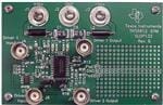
The TI THS6012 500-mA Dual Differential Line Driver Evaluation Module
(EVM) is a complete central office side ADSL high-speed driver circuit. It
consists of the TI THS6012 Dual Differential Line Driver IC, a TI THS4001
High-Speed, Low-Power Operational Amplifier IC, and a number of passive
parts, all mounted on a multilayer circuit board (Figure 1–1). The EVM uses
standard BNC connectors for inputs and outputs and also includes a pad area
for user component connection and testing. It is completely assembled, fully
tested, and ready to use — just connect it to power, a signal source, and a load
(if desired).
Figure 1–1. THS6012 Evaluation Module
+VCC
J3
C1
L1
C8
R8
C2
C13
C14
C9
+
Driver 1
Input
–VCC
GND
J2
J1
J4
+
L2
Driver 1 Output
J5
Texas Instruments
THS6012 EVM
SLOP132
Rev. B
R1
U2
R2
C10
C3
R3
R5
C5
R9
JP1
C7
Driver 2
Input
1-2
Pad1
GND
Pad2
R15
U1
R13
R6
R12
R4
JP2
R10
J6
J7
Driver 2 Output
General Information
�Description
Input power is applied to the EVM through banana jacks J1, J2, and J3. An LC
filter on each power bus isolates the EVM circuits from the external supply. The
schematic for the EVM appears in Figure 1–2.
Figure 1–2. THS6012 Evaluation Module Schematic
J1
J3
J2
L1
0.22 µH
C1
6.8 µF
L2
0.22 µH
C8
6.8 µF
R4
1 kΩ
–15 V
15 V
R3
1 kΩ
15 V
R7
TBD
5
Driver 1
Input
R2
49.9 Ω
3
U2:A
THS6012
2
4
J4
–
+
1
C4
R1
49.9 Ω TBD
C13
0.1 µF
C2
0.1 µF
R5
1 kΩ
Pad1
15 V
–
7
C5
0.1 µF
U1
THS4001
16
1
6
R9
49.9 Ω
+
J6
4
–15 V
R11
TBD
C7
0.1 µF
R10
49.9 Ω
C10
0.1 µF
15 V
JP1
1
C12
TBD
2 OUT
R12
1 kΩ
R13
1 kΩ
R6
1 kΩ
Driver 2
Input
1 OUT
GND
Pad2
C6
TBD
3
R8
12.4 Ω
J5
–15 V
2
Driver 1
Output
C3
0.1 µF
17
18
–
R14
TBD
U2:B
THS6012
19
+
20
Driver 2
Output
C14
0.1 µF
R15
12.4 Ω
C11
TBD
J7
–15 V
C9
0.1 µF
JP2
General Information
1-3
�Description
The THS6012 EVM is equipped with a separate BNC connector for the Driver
1 input and the Driver 2 input. Each input is terminated with a 50-Ω resistor to
provide correct line impedance matching (Figure 1–2). Using a source with a
50-Ω output impedance will create a voltage divider at the EVM inputs. Thus,
accurate knowledge of the source output characteristics is required to
determine proper input signal amplitudes.
Driver outputs are routed through central office side ADSL-standard 12.4-Ω
resistors to provide correct transmission line impedance matching when run
through a 1:2 transformer with a 100-Ω termination. These resistors also allow
separate receivers to view a differential input signal from the transmission line.
All of the amplifiers on the EVM (THS6012 and THS4001) follow the classic
operational amplifier gain equations:
Inverting Gain
+ –RRF
(1)
G
Noninverting Gain
+ 1 ) RRF
(2)
G
The gain of the amplifiers can be easily changed to support different
applications by changing resistor ratios. Any of the components on the EVM
board can be replaced with different values. Also, component pads have been
placed in convenient locations on the PCB (shown as components with the
value X in the schematic) to allow numerous modifications to the basic EVM
configuration. However, care must be taken, because the surface mount
solder pads on the board are somewhat fragile and will not survive a large
number of soldering/desoldering operations.
The THS6012 IC is a current-feedback amplifier (CFB), and, because of this,
extra care must be taken to ensure that a feedback resistor is always included
in the design. In addition, there must never be a capacitor directly in the
feedback path between the noninverting input and the amplifier output.
Disregarding this guideline will likely result in a part that oscillates. The
THS4001 IC amplifier used on the EVM, however, is a classic
voltage-feedback amplifier (VFB) and has no restrictions on resistors or
capacitors in the feedback path. But, to maximize bandwidth, high value
resistors and capacitors should be used with discretion.
Finally, the EVM circuit board is a good example of proper board layout for
high-speed amplifier and PowerPAD designs. It can be used as a guide for
user application layouts.
1-4
General Information
�Input Configuration
1.3 Input Configuration
The THS6012 EVM inputs can be configured in several different ways to
provide a wide variety of circuits to support different applications
(Figure 1–3). Each of the two jumpers on the EVM is a three-pin header that
is used as a SPDT switch by placing a shunt across two pins to select either
of two possible signal routes.
Figure 1–3. THS6012 Evaluation Module Block Diagram
Driver 1
Input
U2: A
Driver 1 Output
THS6012
J4
U1
1
Inverter
1
3
2
3
-
+
2
JP2
J6
-
Positive Driver
JP1
THS4001
Driver 2
Input
J5
U2: B
J7
THS6012
–
Driver 2 Output
Negative Driver
Jumper JP1:
J
J
1–2 — connects the noninverting input of driver 2 (U2: B) to the
THS4001 inverting amplifier (U1) output
2–3 — connects the noninverting input of driver 2 (U2: B) to the input
connector (J6) when jumper JP2 is set appropriately
Jumper JP2:
J
J
1–2 — connects the driver 2 input connector (J6) to the noninverting
input of driver 2 (U2:B) when jumper JP1 is set appropriately
2–3 — connects the driver 2 input connector (J6) to the inverting input
of driver 2 (U2:B) when jumper JP1 is set appropriately
For example, to use a single-ended input, jumper JP1 should be set to 1–2 and
the input signal applied to input connector J4. The output of the THS6012
drivers is a differential signal due to the inverter (U1) and JP1 being set to 1–2.
For a differential source, JP1 should be set to 2–3, JP2 should be set to 1–2
and the differential input signal applied between input connectors J4 and J6.
If JP2 is in the 2–3 position, components C12 and R11 must be installed, R9
must be removed, and a 0-Ω resistor must be installed in the C11 position for
proper operation.
1.4 THS6012 EVM Specifications
Supply voltage range, ± VCC . . . . . . . . . . . . . . . . . . . . . . . . . . . . . . . . . . . . . . . . . . . . ± 5 V to ± 15 V
Supply current, ICC . . . . . . . . . . . . . . . . . . . . . . . . . . . . . . . . . . . . . . . . . . . . . . . . . . . . . . . . . . . 26 mA
Input voltage, VI . . . . . . . . . . . . . . . . . . . . . . . . . . . . . . . . . . . . . . . . . . . . . . . . . . . . . . . . . ± VCC, max
Output drive, THS6012 Drivers, IO . . . . . . . . . . . . . . . . . . . . . . . . . . . . . . . . . . . . 500 mA, typ each
Continuous total power dissipation at TA = 25°C (THS6012), . . . . . . . . . . . . . . . . . . . 5.8 W, max
For complete THS6012 amplifier IC specifications, parameter measurement
information, and additional application information, see the THS6012 data
sheet, TI Literature Number SLOS226.
General Information
1-5
�Using The THS6012 EVM
1.5 Using The THS6012 EVM
The THS6012 EVM operates from a split power supply with voltages ranging
from ± 5 V to ± 15 V. The use of a single supply for this EVM is not
recommended. As shipped, the output of driver 1 is equal to a noninverting
gain of 2 when using the single-ended input mode. The output of driver 2 is
equal to an inverting gain of 2 under the same conditions. An oscilloscope is
typically used to view and analyze the EVM output signals.
1) Ensure that all power supplies are set to OFF before making power supply
connections to the THS6012 EVM.
2) Select the operating voltage for the EVM and connect appropriate split
power supplies to the banana jacks on the module marked +VCC (J1) and
–VCC (J3).
3) Connect the power supply ground to the module banana jack marked
GND (J2).
4) Connect an oscilloscope probe to U2, pin2. This is the driver 1 amplifier
output. Connecting directly to the DRIVER 1 OUTPUT BNC connector
(J5) with a 50-Ω nominal impedance cable and probe is not
recommended. The source impedance of driver 1 is only 12.4 Ω; such a
connection could cause reflections to occur at high frequencies and is not
a true measurement of the amplifier performance.
5) Set jumper J1 to the 1–2 position.
6) Set jumper J2 to the 1–2 position.
7) Set the power supply to ON
8) Connect a signal input to the DRIVER 1 INPUT BNC (J4).
Each input connector on this EVM is terminated with a 50-Ω resistor to ground.
With a 50-Ω source impedance, the voltage seen by the THS6012 amplifier
IC on the EVM will be 1/2 the source signal voltage applied to the EVM input
connector.
9) Verify the output signal on the oscilloscope. With a high-impedance scope
probe, the output signal should be twice the source amplitude. When
connected to J7 (Driver 2 output), the signal should be 180° phase shifted
from the Driver 1 output (J5).
1-6
General Information
�THS6012 EVM Performance
1.6 THS6012 EVM Performance
Figure 1–4 shows the typical frequency response of the THS6012 EVM drivers
when properly loaded. This data was collected using a single-ended input with
a 50-Ω differential load connected between the driver outputs, as shown in the
test circuit of Figure 1–5.
Typical unity gain bandwidth with a ± 15 V power supply is 100 MHz for both
drivers. With a ± 5 V power supply, typical unity gain bandwidth is also
100 MHz for both drivers. The difference between the output signals of driver
1 and driver 2 is primarily due to the high-frequency characteristics of the
inverting amplifier (U1). Component values can be changed to cause the two
responses to track more closely, but since ADSL signals are limited to 2 MHz
and below, the high-frequency imbalance can usually be ignored.
Figure 1–4. THS6012 EVM Driver Frequency Response With a 50-Ω Load
OUTPUT LEVEL
vs
FREQUENCY
OUTPUT LEVEL
vs
FREQUENCY
7
7
Driver 2 Ouput
Driver 2 Ouput
6
6
Driver 1 Input
5
Output Level – dB
Output Level – dB
5
4
3
2
1
0
–1
–2
VCC = ± 5V
VI(PP) = 2 V
RL = 50 Ω Differential
JP1 : 1–2
JP2 : 1–2
–3
100k
1M
3
2
1
0
–1
–2
100M
10M
f – Frequency – Hz
500M
Driver 1 Input
4
VCC = ± 15V
VI(PP) = 2 V
RL = 50 Ω Differential
JP1 : 1–2
JP2 : 1–2
–3
100k
1M
100M
10M
f – Frequency – Hz
500M
Figure 1–5. THS6012 EVM Driver Frequency Response Test Circuit
1 OUT
Pad 1
R8
12.4 Ω
Driver 1 Output
J5
RL
User Pad Area
25 Ω
GND
Driver 2 Output
2 OUT
Pad 2
R15
12.4 Ω
J7
General Information
1-7
�General High-Speed Amplifier Design Considerations
1.7 General High-Speed Amplifier Design Considerations
The THS6012 EVM layout has been designed and optimized for use with
high-speed signals and can be used as an example when designing THS6012
applications. Careful attention has been given to component selection,
grounding, power supply bypassing, and signal path layout. Disregard of these
basic design considerations could result in less than optimum performance of
the THS6012 500-mA dual differential line driver IC.
Surface-mount components were selected because of the extremely low lead
inductance associated with this technology. Also, because surface-mount
components are physically small, the layout can be very compact. This helps
minimize both stray inductance and capacitance.
Tantalum power supply bypass capacitors (C1 and C8) at the power input pads
help supply currents for rapid, large signal changes at the amplifier output. The
0.1 µF power supply bypass capacitors (C2, C3, C5, and C7) are placed as
close as possible to the IC power input pins in order to keep the PCB trace
inductance to a minimum. This improves high-frequency bypassing and
reduces harmonic distortion. Additional 0.1 µF capacitors (C13 and C14) are
placed between +VCC and –VCC. This helps minimize the harmonic distortion
of the amplifiers.
A proper ground plane should always be used with high-speed circuit design.
This provides low-inductive ground connections for return current paths.
Special attention is needed for the inverting input pins. Stray capacitance at
these pins can seriously degrade the performance of the amplifiers. In
addition, ground plane coupling into these pins can cause noise to appear at
the outputs of the amplifiers. This is especially important for the inverting pin
while the amplifier is operating in the noninverting mode. Because the voltage
at this pin swings directly with the noninverting input voltage, any stray
capacitance would allow currents to flow into the ground plane, causing
possible gain error and/or oscillation. Capacitance variations at the amplifier
IC input pin of less than 1 pF can significantly affect the response of the
amplifier.
In general, it is always best to keep signal lines as short and as straight as
possible. Sharp 90_ corners should generally be avoided — round corners or
a series of 45_ bends should be used, instead. Stripline techniques should
also be incorporated when signal lines are greater than 3 inches in length.
These traces should be designed with a characteristic impedance of either
50 Ω or 75 Ω, as required by the application. Such signal lines should also be
properly terminated with an appropriate resistor.
Finally, proper termination of all inputs and outputs should be incorporated into
the layout. Unterminated lines, such as coaxial cable, can appear to be a
reactive load to the amplifier IC. By terminating a transmission line with its
characteristic impedance, the amplifier’s load then appears to be purely
resistive, and reflections are absorbed at each end of the line. Another
advantage of using an output termination resistor is that capacitive loads are
isolated from the amplifier output. This isolation helps minimize the reduction
in amplifier phase-margin and improves the amplifier stability for improved
performance such as reduced peaking and settling times.
1-8
General Information
�General PowerPAD Design Considerations
1.8 General PowerPAD Design Considerations
The THS6012 IC is mounted in a special package incorporating a thermal pad
that transfers heat from the IC die directly to the PCB. The PowerPAD package
is constructed using a downset leadframe. The die is mounted on the
leadframe but is electrically isolated from it. The bottom surface of the lead
frame is exposed as a metal thermal pad on the underside of the package and
makes physical contact with the PCB. Because this thermal pad is in direct
physical contact with both the die and the PCB, excellent thermal performance
can be achieved by providing a good thermal path away from the thermal pad
mounting point on the PCB.
Although there are many ways to properly heatsink this device, the following
steps illustrate the recommended approach as used on the THS6012 EVM,
which is built on a multilayer PCB with an internal ground plane.
1) Prepare the PCB with a top side etch pattern as shown in Figure 1–6.
There should be etch for the leads as well as etch for the thermal pad.
Figure 1–6. PowerPAD PCB Etch and Via Pattern – Minimum Requirements
Thermal pad area (0.19 x 0.21) with 18 vias
(Via diameter = 13 mils)
2) Place 18 holes in the area of the thermal pad. These holes should be 13
mils in diameter. They are kept small so that solder wicking through the
holes is not a problem during reflow.
3) Additional vias may be placed anywhere along the thermal plane outside
of the thermal pad area. This will help dissipate the heat generated from
the THS6012. These additional vias may be larger than the 13 mil diameter vias directly under the thermal pad. They can be larger because they
are not in the thermal-pad area to be soldered, therefore, wicking is generally not a problem.
4) Connect all holes to the internal ground plane.
5) When connecting these holes to the ground plane, DO NOT use the typical
web or spoke via connection methodology. Web connections have a high
thermal resistance connection that is useful for slowing the heat transfer
during soldering operations. This makes the soldering of vias that have
plane connections easier. However, in this application, low thermal
resistance is desired for the most efficient heat transfer. Therefore, the
holes under the THS6012 package should make their connection to the
internal ground plane with a complete connection around the entire
circumference of the plated through hole.
General Information
1-9
�General PowerPAD Design Considerations
6) The top-side solder mask should leave exposed the terminals of the
package and the thermal pad area with its 18 holes. The bottom-side
solder mask should cover the 18 holes of the thermal pad area. This
eliminates the solder from being pulled away from the thermal pad area
during the reflow process.
7) Apply solder paste to the exposed thermal pad area and all of the
operational amplifier terminals.
8) With these preparatory steps in place, the THS6012 is simply placed in
position and run through the solder reflow operation as any standard
surface mount component. This results in a part that is properly installed.
The actual thermal performance achieved with the THS6012 in its PowerPAD
package depends on the application. In the example above, if the size of the
internal ground plane is approximately 3 inches × 3 inches, then the expected
thermal coefficient, θJA, is about 21.5_C/W. For a given θJA, the maximum
power dissipation, shown in Figure 1–7, is calculated by the following formula:
P
D
+
Where:
ǒ Ǔ
T
MAX
–T
q JA
A
PD = Maximum power dissipation of THS6012 (watts)
TMAX = Absolute maximum junction temperature (150°C)
TA
= Free-ambient air temperature (°C)
θJA = θJC + θCA
θJC = Thermal coefficient from junction to case ( 0.37°C/W)
θCA = Thermal coefficient from case to ambient air
Figure 1–7. Maximum Power Dissipation vs. Free-Air Temperature
MAXIMUM POWER DISSIPATION
vs
FREE-AIR TEMPERATURE
9
Tj = 150°C
PCB Size = 3” x 3”
No Air Flow
Maximum Power Dissipation – W
8
7
θJA = 21.5°C/W
2 oz Trace and
Copper Pad
with Solder
6
5
4
3
2
θJA = 43.9°C/W
2 oz Trace and Copper Pad
without Solder
1
0
–40
–20
0
20
40
60
80
100
TA – Free-Air Temperature – °C
1-10
General Information
�General PowerPAD Design Considerations
Even though the THS6012 EVM PCB is larger than the one in the example
above, the results should correlate very well because the traces and the vias
of the EVM PCB interrupt the thermal continuity of the ground plane. The
THS6012 EVM is a good example of proper thermal management when using
PowerPAD-mounted devices.
Correct PCB layout and manufacturing techniques are critical for achieving
adequate transfer of heat away from the PowerPAD IC package. More details
on proper board layout can be found in the THS6012 500-mA DUAL
DIFFERENTIAL LINE DRIVER data sheet (SLOS226). For more general
information on the PowerPAD package and its thermal characteristics, see the
Texas Instruments Technical Brief, PowerPAD Thermally Enhanced Package
(SLMA002).
General Information
1-11
�1-12
General Information
�Chapter 2
Reference
This chapter includes a parts list and PCB layout illustrations for the THS6012
EVM.
Topic
Page
2.1
THS6012 Dual Differential Line Drivers and Receivers
EVM Parts List . . . . . . . . . . . . . . . . . . . . . . . . . . . . . . . . . . . . . . . . . . 2–2
2.2
THS6012 EVM Board Layouts
. . . . . . . . . . . . . . . . . . . . . . . . . . . . . 2–3
Reference
2-1
�THS6012 Dual Differential Line Drivers EVM Parts List
2.1 THS6012 Dual Differential Line Drivers EVM Parts List
Table 2–1. THS6012 EVM Parts List
Reference
Description
Size
Quantity
Manufacturer/Distributor
Part Number
2
(SPRAGUE) 293D685X9035D2T
8
(MuRate) GRM40-X7R104K25
C1, C8
CAPACITOR, 6.8 µF, 35 V, 20%, TANTALUM,
SM
C2, C3, C5,
C7, C9, C10,
C13, C14
CAPACITOR, 0.1 µF, CERAMIC, 10%, SM
L1,L2
INDUCTOR, 0.22 µH AXIAL, THRU HOLE
2
(DELEVAN) DN41221/
(DIGI-KEY) DN411221-ND
J4,J5,J6, J7
JACK, BNC, PC-MOUNT (AMPHONEL)
4
(MOUSER) 523-31-5329
J1,J2,J3
JACK, BANANA RECEPTANCE, FOR 0.25″
DIA. HOLE
2
JP1,JP2
HEADER, 3 PIN, 0.1″ CTRS., 0.025″ SQ. PINS
2
R2, R9
RESISTOR, 49.9 OHMS, 1/10W, 1% SM
0805
2
R1, R10
RESISTOR, 49.9 OHMS, 1/8W, 1% SM
1206
4
R3, R4, R5,
R6, R12, R13
RESISTOR, 1 kOHM, 1/10W, 1% SM
0805
6
R8, R15
RESISTOR, 12.4 OHMS, 1/8W, 1% SM
1206
2
U2
IC, THS6012CDWP
U1
IC, OP AMP, THS4001CD
R7, R14
R11
C4, C6, C11,
C12
0805
1
(TI) THS6012CDWP
SOIC-8
1
(TI) THS4001CD
RESISTOR, X OHMS, 1/8W, 1%, SM†
RESISTOR, X OHMS, 1/10W, 1%, SM†
1206
2
0805
1
CAPACITOR, X µF, 10% CERAMIC†
0805
4
4-40 TREAD HEX STANDOFFS, 0.625″
LENGTH, 0.250 O.D.
4
4-40 TREAD HEX STANDOFFS SCREWS
4
(MOUSER) 534-1804
PCB1
PCB, THS6012 EVM SLOP132
1
† The values of these components are to be determined by the user in accordance with the application requirements.
2-2
Reference
�THS6012 EVM Board Layouts
2.2 THS6012 EVM Board Layouts
Board layout examples of the THS6012 EVM PCB are shown in the following
illustrations. They are not to scale and appear here only as a reference.
Figure 2–1. THS6012 EVM Component Placement Silkscreen and Layout
+VCC
J3
C1
L1
C8
J4
+
L2
J5
Driver 1 Output
Texas Instruments
THS6012 EVM
SLOP132
Rev. B
R1
U2
R2
C10
R3
U1
R4
C11
C5
R9
JP1
C7
Driver 2
Input
JP2
R12
Pad1
GND
Pad2
C12
R13
R14
R15
R11
C3
C4
R5
C6
R6
14
C9
R7
R8
C2
13
+
Driver 1
Input
–VCC
GND
J2
J1
R10
J6
J7
Driver 2 Output
Figure 2–2. THS6012 EVM PC Board: Layer 1 — Top Side Layout
Reference
2-3
�THS6012 EVM Board Layouts
Figure 2–3. THS6012 EVM PC Board: Layer 2 — Back Side Ground Plane Layer
Figure 2–4. THS6012 EVM PC Board: Solder Mask — Back Side
2-4
Reference
�