THS6184
RHF 24-Pin
PWP 20-Pin
www.ti.com ................................................................................................................................................. SLLS635D – AUGUST 2005 – REVISED JANUARY 2009
DUAL-PORT, LOW-POWER DIFFERENTIAL
xDSL LINE DRIVER AMPLIFIERS
FEATURES
DESCRIPTION
1
• Trimmed Low-Power Consumption
– 4.2-mA/amp Full Bias Mode; 4.8 mA Max
– 3.2-mA/amp Mid Bias Mode; 3.7 mA Max
– 2.15-mA/amp Low Bias Mode; 2.5 mA Max
– Shutdown Mode and IADJ Pin for Variable
Bias
• Low Noise
– 3-nV/√Hz Voltage Noise
– 5.9-pA/√Hz Inverting Current Noise
– 1.2-pA/√Hz Noninverting Current Noise
• Low MTPR Distortion
– –74 dB with ADSL and ADSL2
– –71 dB with ADSL2+ and –70 dB with
ADSL2++
• –83 dBc THD (1 MHz, 100-Ω Differential)
• High Output Current: >415 mA (25-Ω Load)
• Wide Output Swing: 44 VPP (±12-V, 200-Ω
Differential)
• Wide Bandwidth: 30 MHz (Gain = 5)
• Wide Power Supply Range: ±4 V to ±16 V
The THS6184 is a dual-port, low-power current
feedback differential line driver amplifier system ideal
for xDSL systems. Its extremely low-power
dissipation is ideal for ADSL, ADSL2, ADSL2+, and
ADSL2++ systems that must achieve high densities in
ADSL central office applications by combining two
ports, or four amplifiers, into one package.
23
The unique architecture of the THS6184 allows the
trimmed quiescent current to be much lower than
existing line drivers while still achieving high linearity.
Distortion at these low-power levels is good with
–83-dBc THD at 1 MHz with the low bias mode of 4.2
mA/port. Fixed and variable multiple-bias settings of
the amplifiers allows for enhanced power savings for
line lengths where the full performance of the
amplifier is not required.
The wide output swing of 44-VPP differentially with
±12-V power supplies coupled with over 415-mA
current drive allow for wide dynamic range, keeping
distortion minimized. With a low 3-nV/√Hz voltage
noise coupled with a low 5.9-pA/√Hz inverting current
noise, the THS6184 increases the sensitivity of the
receive signals allowing for better margins and reach.
APPLICATIONS
•
Ideal For Power Sensitive, High Density ADSL,
ADSL2, ADSL2+, and ADSL2++ Systems
12 V
CODEC
V IN +
+
30.1 Ω
Line Power = ADSL2: 19.8 dBm
−
ADSL2+: 20.4 dBm
ADSL2++: 21.1 dBm
4.99 kΩ
1:1
1.15 kΩ
1 μF
33 nF
Line:
100 Ω
0.1 μF
4.99 kΩ
−
CODEC
V IN−
+
30.1 Ω
−12 V
Figure 1. Typical Line Driver Circuit Using One Port of THS6184
1
2
3
Please be aware that an important notice concerning availability, standard warranty, and use in critical applications of Texas
Instruments semiconductor products and disclaimers thereto appears at the end of this data sheet.
PowerPAD is a trademark of Texas Instruments.
All other trademarks are the property of their respective owners.
PRODUCTION DATA information is current as of publication date.
Products conform to specifications per the terms of the Texas
Instruments standard warranty. Production processing does not
necessarily include testing of all parameters.
Copyright © 2005–2009, Texas Instruments Incorporated
�THS6184
SLLS635D – AUGUST 2005 – REVISED JANUARY 2009 ................................................................................................................................................. www.ti.com
This integrated circuit can be damaged by ESD. Texas Instruments recommends that all integrated circuits be handled with
appropriate precautions. Failure to observe proper handling and installation procedures can cause damage.
ESD damage can range from subtle performance degradation to complete device failure. Precision integrated circuits may be more
susceptible to damage because very small parametric changes could cause the device not to meet its published specifications.
ABSOLUTE MAXIMUM RATINGS (1)
Over operating free-air temperature range (unless otherwise noted).
UNIT
VS– to VS+
Supply voltage
33 V
VI
Input voltage
±VS
VID
Differential input voltage
IO
Output current – Static DC (2)
±2 V
±100 mA
Continuous power dissipation
See Dissipation Rating Table
Maximum junction temperature, any condition
TJ
(3)
150°C
Maximum junction temperature, continuous operation, long term reliability (4)
Tstg
130°C
Storage temperature range
–65°C to 150°C
Lead temperature 1,6 mm (1/16 inch) from case for 10 seconds
ESD ratings
(1)
(2)
(3)
(4)
300°C
HBM
900 V
CDM
1500 V
MM
100 V
Stresses above those listed under absolute maximum ratings may cause permanent damage to the device. These are stress ratings
only, and functional operation of the device at these or any other conditions beyond those indicated under recommended operating
conditions is not implied Exposure to absolute maximum rated conditions for extended periods may degrade device reliability.
The THS6184 incorporates a PowerPAD™ on the underside of the chip. This acts as a heatsink and must be connected to a thermally
dissipating plane for proper power dissipation. Failure to do so may result in exceeding the maximum junction temperature which could
permanently damage the device. See TI Technical Brief SLMA002 for more information about utilizing the PowerPAD™ thermally
enhanced package. Under high frequency ac operation (>10 kHz), the short-term output current capability is much greater than the
continuous DC output current rating. This short-term output current rating is about 8.5× the dc capability, or about ±850 mA.
The absolute maximum junction temperature under any condition is limited by the constraints of the silicon process.
The absolute maximum junction temperature for continuous operation is limited by the package constraints. Continuous operation above
this temperature may result in reduced reliability and/or lifetime of the device.
DISSIPATION RATINGS
PACKAGE
(1)
(2)
(3)
2
θJC (°C/W)
QFN-24 (RHF)
1.7
HTSSOP-20 (PWP)
27.5
POWER RATING (2)
TJ = 130°C
θJA (°C/W) (1)
32
(3)
45
TA = 25°C
TA = 85°C
3.3 W
1.4 W
2.3 W
1W
This data was taken using a 4-layer, 3-inch × 3-inch test PCB with the PowerPAD soldered to the PCB. For high power dissipation
applications, soldering the PowerPAD to the PCB is required. Failure to do so may result in reduced reliability and/or lifetime of the
device. See TI technical brief SLMA002 for more information about utilizing the PowerPAD thermally enhanced package.
Power rating is determined with a junction temperature of 130°C. This is the point where distortion starts to substantially increase and
long-term reliability starts to be reduced. Thermal management of the final PCB should strive to keep the junction temperature at or
below 125°C for best performance and reliability.
If the PowerPAD is not soldered to the PCB, the θJA increases to 74°C/W for the RHF package.
Submit Documentation Feedback
Copyright © 2005–2009, Texas Instruments Incorporated
Product Folder Link(s): THS6184
�THS6184
www.ti.com ................................................................................................................................................. SLLS635D – AUGUST 2005 – REVISED JANUARY 2009
PACKAGING/ORDERING INFORMATION (1)
PACKAGED DEVICES (2)
DEVICE MARKING
PACKAGE TYPE
6184
QFN-24
THS6184
PowerPAD™ HTSSOP-20
THS6184RHFT
THS6184RHFR
THS6184PWP
THS6184PWPR
(1)
(2)
TRANSPORT MEDIA, QUANTITY
Tape and reel, 250
Tape and reel, 3000
Rails, 70
Tape and reel, 2000
For the most current package and ordering information, see the Package Option Addendum at the end of this document, or see the TI
website at www.ti.com.
The thermal pad is electrically isolated from all other pins.
PIN CONFIGURATION
1
20
VS−
BIAS-2/D1D2
2
19
D1 OUT
D1 IN+
3
18
D1 IN−
D2 IN+
4
17
D2 IN−
GND
5
16
D2 OUT
IADJ
6
15
D3 OUT
D3 IN+
7
14
D3 IN−
D4 IN+
8
13
D4 IN−
BIAS-2/D3D4
9
12
D4 OUT
BIAS-1/D3D4
10
11
VS+
19
D1 IN−
D2 IN+
2
18
D2 IN−
GND
3
17
D2 OUT
IADJ
4
16
D3 OUT
NC
5
15
D3 IN−
D3 IN+
6
14
D4 IN−
D4 IN+
7
13
D4 OUT
D
PA
er
w
BIAS-1/D3D4
VS+
D
See Notes
NC
10 11 12
NC
9
BIAS-2/D3D4
Po
8
er
1
TM
D1 IN+
PA
24 23 22 21 20
TM
BIAS-1/D1D2
Po
w
NC
PWP Package
(Top View)
D1 OUT
BIAS-1/D1D2
VS−
BIAS-2/D1D2
RHF Package
(Top View)
NC − No internal connection
See Notes
A.
The THS6184 defaults to the FULL BIAS state if no signal is present on the BIAS pins.
B.
The PowerPAD is electrically isolated from all other pins and can be connected to any potential voltage range from
VS– to VS+. Typically, the PowerPAD is connected to the GND plane as this plane tends to be physically the largest
and able to dissipate the most amount of heat.
C.
The GND pin range is from VS– to (VS+ – 2.5 V).
D.
The IADJ (RHF pin 4, PWP pin 6) must be connected to GND (RHF pin 3, PWP pin 5) for full bias as used in the
specification tables.
RECOMMENDED OPERATING CONDITIONS
Over operating free-air temperature range (unless otherwise noted).
Dual supply
MIN
MAX
±4
±16
8
32
VS– to VS+
Supply voltage
TA
Operating free-air temperature
–40
85
TJ
Operating junction temperature, continuous operating temperature
–40
130
Single supply
Submit Documentation Feedback
Copyright © 2005–2009, Texas Instruments Incorporated
Product Folder Link(s): THS6184
UNIT
V
°C
3
�THS6184
SLLS635D – AUGUST 2005 – REVISED JANUARY 2009 ................................................................................................................................................. www.ti.com
ELECTRICAL CHARACTERISTICS
At VS = ±12 V: RF = 3 kΩ, RL = 50 Ω, G = 5, Radj = 0 Ω, full bias (unless otherwise noted) each amplifier independently tested.
TYP
PARAMETER
CONDITIONS
25°C
OVER TEMPERATURE
25°C
0°C to
70°C
–40°C to
85°C
UNITS
MIN/
MAX
MHz
Typ
AC PERFORMANCE
Small-signal bandwidth,
–3 dB (VO = 100 mVRMS)
G = 1, RF = 4 kΩ
50
G = 2, RF = 3.5 kΩ
40
G = 5, RF = 3 kΩ
30
G = 10, RF = 3 kΩ
22
0.1-dB bandwidth flatness
G=5
8
MHz
Typ
Large-signal bandwidth
G = 5, VO = 10 VPP
17.5
MHz
Typ
G = 5, VO = 16-V step, single-ended
340
V/µs
Typ
G = 5, VO = 16-V step, differential
560
V/µs
Typ
G = 5, VO = 2 VPP
12
ns
Typ
dBc
Typ
dBc
Typ
dBc
Typ
dBc
Typ
Slew rate (25% to 75% level)
Rise and fall time
2nd harmonic
3rd harmonic
G = 5,
VO = 2 VPP,
f = 1 MHz,
Differential
Harmonic distortion
2nd harmonic
3rd harmonic
Multitone Power Ratio (MTPR) 160 kHz to
ADSL limit (1)
G = 5,
VO = 2 VPP,
f = 4 MHz,
Differential
RL = 100 Ω
–89
RL = 50 Ω
–85
RL = 100 Ω
–85
RL = 50 Ω
–79
RL = 100 Ω
–83
RL = 50 Ω
–80
RL = 100 Ω
–63
RL = 50 Ω
–55
G = 10, PLine = 19.8 dBm, ADSL2
–74
G = 10, PLine = 20.4 dBm, ADSL2+
–71
G = 10, PLine = 21.1 dBm, ADSL2++
–70
G = 10, PLine = 19.8 dBm, ADSL2
–93
Receive Band Spill-Over 25kHz to 138 kHz G = 10, PLine = 20.4 dBm, ADSL2+
G = 10, PLine = 21.1 dBm, ADSL2++
–91
–90
Input voltage noise
f > 10 kHz
3
nV/√Hz
Typ
Inverting current noise
f > 10 kHz
5.9
pA/√Hz
Typ
Noninverting current noise
f > 10 kHz
1.2
pA/√Hz
Typ
DC PERFORMANCE
Open-loop transimpedance gain
RL = 100 Ω
6
Input offset voltage
±10
Average offset voltage drift
Input offset voltage matching
±22
±25
±25
±0.5
±3
±5
±5
±1
±10
±15
±15
±7
Channels 1 to 2 and 3 to 4 only
Noninverting Input bias current
Noninverting input bias current drift
Inverting input bias current
Inverting input bias current drift
±150
±1
±10
±15
±15
±150
MΩ
Typ
mV
Max
µV/°C
Typ
mV
Max
µA
Max
nA/°C
Typ
µA
Max
nA/°C
Typ
Min
INPUT CHARACTERISTICS
Common-mode input range
±10.2
±9.5
±9.4
±9.4
V
Common-mode rejection ratio
67
60
58
58
dB
Min
Noninverting input resistance
500||2
kΩ||pF
Typ
160
Ω
Typ
Inverting input resistance
OUTPUT CHARACTERISTICS
(1)
4
Test circuit is as shown in Figure 2. Transformer insertion loss = 0.4 dB. ADSL2++ is still considered a proposal and is not an official
standard at this time.
Submit Documentation Feedback
Copyright © 2005–2009, Texas Instruments Incorporated
Product Folder Link(s): THS6184
�THS6184
www.ti.com ................................................................................................................................................. SLLS635D – AUGUST 2005 – REVISED JANUARY 2009
ELECTRICAL CHARACTERISTICS (continued)
At VS = ±12 V: RF = 3 kΩ, RL = 50 Ω, G = 5, Radj = 0 Ω, full bias (unless otherwise noted) each amplifier independently tested.
TYP
PARAMETER
CONDITIONS
RL = 50 Ω
Output voltage swing
UNITS
MIN/
MAX
+11
V
Typ
–11
V
Typ
25°C
RL = 100 Ω
RL = 25 Ω
OVER TEMPERATURE
25°C
0°C to
70°C
–40°C to
85°C
10.8
10.4
10.3
10.3
V
Min
–10.8
–10.4
–10.3
–10.3
V
Max
+10.4
+9.8
+9.7
+9.7
V
Min
–10.35
–9.7
–9.6
–9.6
V
Max
Min
Output current (sourcing)
RL = 25 Ω
416
392
388
388
mA
Output current (sinking)
RL = 25 Ω
414
388
384
384
mA
Min
mA
Typ
Short circuit output Current
Output impedance
±850
0.2
Ω
Typ
D1 to D2, D3 to D4
–40
dB
Typ
D1 to D3, D2 to D4
–70
dB
Typ
f = 1 MHz
f = 1 MHz,
VO = 2 VPP
Crosstalk
POWER SUPPLY
Maximum operating voltage
±16
±16
±16
V
Max
Minimum operating voltage
±4
±4
±4
V
Min
mA
Max
mA
Min
mA
Max
Maximum Is+ quiescent current
Minimum Is+ quiescent current
Maximum ls- quiescent current
Per amplifier, Full (Bias-1=0, Bias-2 = 0)
4.3
4.9
5.1
5.2
Per amplifier, Mid (Bias-1=1, Bias-2 = 0)
3.3
3.8
4.0
4.1
Per amplifier, Low (Bias-1=0, Bias-2 = 1)
2.2
2.6
2.8
2.9
Per amplifier, Off (Bias-1=1, Bias-2 = 1)
0.2
0.3
0.4
0.4
Per amplifier, Full (Bias-1=0, Bias-2 = 0)
4.3
3.8
3.6
3.6
Per amplifier, Full (Bias-1=0, Bias-2 = 0)
4.1
4.7
4.9
5
Per amplifier, Mid (Bias-1=1, Bias-2 = 0)
3.1
3.6
3.8
3.9
Per amplifier, Low (Bias-1=0, Bias-2 = 1)
2.1
2.4
2.6
2.7
Per amplifier, Off (Bias-1=1, Bias-2 = 1)
0.01
0.1
0.15
0.15
Minimum Is- quiescent current
Per amplifier, Full Bias
4.1
3.6
3.5
3.5
Current through GND pin
Per amplifier, Full (Bias-1 = 0, Bias-2 = 0)
0.2
Power supply rejection (+PSRR)
VS+ = 13 V to 11 V, VS– = –12 V
78
72
70
Power supply rejection (-PSRR)
VS+ = 12 V, VS– = –13 V to –11 V
73
67
65
mA
Min
mA
Typ
69
dB
Min
64
dB
Min
LOGIC CHARACTERISTICS
Bias control pin logic threshold
Bias pin quiescent current
Turn on time delay(t(ON))
Turn off time delay (t(Off))
Logic 1, with respect to GND pin
(2)
≥2.6
V
Typ
Logic 0, with respect to GND pin
(2)
≤0.8
V
Typ
µA
Max
µs
Typ
50
kΩ
Typ
10||5
kΩ||pF
Typ
Bias-X =0.5 V (Logic 0)
1
10
15
15
Bias-X = 3.3 V (Logic 1)
10
20
30
30
Time for IS to reach 50% of final value
Bias pin input impedance
Amplifier output impedance
(2)
Off (Bias-1 = 1, Bias-2 = 1)
1
1
GND pin useable range is from Vs– to (Vs+ – 2.5 V).
Table 1. LOGIC TABLE (1)
(1)
BIAS-1
BIAS-2
FUNCTION
0
0
Full bias mode
Amplifiers ON with lowest distortion possible (default state)
DESCRIPTION
1
0
Mid bias mode
Amplifiers ON with power savings with a reduction in distortion performance
0
1
Low bias mode
Amplifiers ON with enhanced power savings and a reduction of performance
1
1
Shutdown mode
Amplifiers OFF and output has high impedance
Logic pins should not be left floating and should be held at a logic-0 or a logic-1 by external circuitry.
Submit Documentation Feedback
Copyright © 2005–2009, Texas Instruments Incorporated
Product Folder Link(s): THS6184
5
�THS6184
SLLS635D – AUGUST 2005 – REVISED JANUARY 2009 ................................................................................................................................................. www.ti.com
ELECTRICAL CHARACTERISTICS
At VS = ±5 V: RF = 3 kΩ, RL = 50 Ω, G = 5, Radj = 0, full bias (unless otherwise noted). Each amplifier independently tested
TYP
PARAMETER
CONDITIONS
25°C
OVER TEMPERATURE
25°C
0°C to
70°C
–40°C
to 85°C
UNITS
MIN/
MAX
MHz
Typ
AC PERFORMANCE
Small-signal bandwidth,
–3 dB (VO = 100 mVPP)
G = 1, RF = 4 kΩ
55
G = 2, RF = 3.5 kΩ
45
G = 5, RF = 3 kΩ
35
G = 10, RF = 3 kΩ
25
0.1-dB bandwidth flatness
G=5
7
MHz
Typ
Large-signal bandwidth
G = 5, VO = 4 VPP
27
MHz
Typ
G = 5, VO = 4-V Step, Single-ended
275
V/µs
Typ
G = 5, VO = 4-V Step, Differential
450
V/µs
Typ
G = 5, VO = 2 VPP
10
ns
Typ
dBc
Typ
dBc
Typ
Slew rate (25% to 75% level)
Rise and fall time
2nd harmonic
3rd harmonic
G = 5,
VO = 2 VPP,
f = 1 MHz,
Differential
Harmonic distortion
2nd harmonic
3rd harmonic
G = 5,
VO = 2 VPP,
f = 4 MHz,
Differential
RL = 100 Ω
–88
RL = 50 Ω
–86
RL = 100 Ω
–83
RL = 50 Ω
–76
RL = 100 Ω
–84
RL = 50 Ω
–81
RL = 100 Ω
–62
RL = 50 Ω
–53
Input voltage noise
f > 10 kHz
3
nV/√Hz
Typ
Inverting current noise
f > 10 kHz
5.9
pA/√Hz
Typ
Noninverting current noise
f > 10 kHz
1.2
pA/√Hz
Typ
DC PERFORMANCE
Open-loop transimpedance gain
RL = 100 Ω
5
Input offset voltage
±9
±21
±24
±24
±0.5
±3
±5
±5
±1
±10
±15
±15
Average offset voltage drift
Input offset voltage matching
±7
Channels 1 to 2 and 3 to 4 only
Noninverting input bias current
Noninverting input bias current drift
±150
Inverting input bias current
±1
Inverting input bias current drift
±10
±15
±15
±150
MΩ
Typ
mV
Max
µV/°C
Typ
mV
Max
µA
Max
nA/°C
Typ
µA
Max
nA/°C
Typ
Min
INPUT CHARACTERISTICS
Common-mode input range
±3.5
±2.5
±2.4
±2.4
V
Common-mode rejection ratio
65
58
56
56
dB
Min
Noninverting Input resistance
500||2
kΩ||pF
Typ
180
Ω
Typ
4.1
V
Typ
V
Typ
Inverting input resistance
OUTPUT CHARACTERISTICS
RL = 100 Ω
Output voltage swing
–4.1
RL = 50 Ω
RL = 25 Ω
4
3.8
3.7
3.7
V
Min
–4
–3.8
–3.7
–3.7
V
Max
4
3.7
3.6
3.6
V
Min
–4
–3.7
–3.6
–3.6
V
Max
Output current (sourcing)
RL = 5 Ω
400
mA
Typ
Output current (sinking)
RL = 5 Ω
400
mA
Typ
±750
mA
Typ
0.2
Ω
Typ
Short-circuit output current
Output impedance
6
f = 1 MHz
Submit Documentation Feedback
Copyright © 2005–2009, Texas Instruments Incorporated
Product Folder Link(s): THS6184
�THS6184
www.ti.com ................................................................................................................................................. SLLS635D – AUGUST 2005 – REVISED JANUARY 2009
ELECTRICAL CHARACTERISTICS (continued)
At VS = ±5 V: RF = 3 kΩ, RL = 50 Ω, G = 5, Radj = 0, full bias (unless otherwise noted). Each amplifier independently tested
TYP
PARAMETER
CONDITIONS
f = 1 MHz,
VO = 2 VPP
Crosstalk
25°C
OVER TEMPERATURE
25°C
0°C to
70°C
–40°C
to 85°C
UNITS
MIN/
MAX
D1 to D2, D3 to D4
–35
dB
Typ
D1 to D3, D2 to D4
–70
dB
Typ
Max
POWER SUPPLY
Maximum operating voltage
±16
±16
±16
V
Minimum operating voltage
±4
±4
±4
V
Min
4.4
4.5
4.6
mA
Max
mA
Typ
Maximum Is+ quiescent current
Minimum Is+ quiescent current
Maximum ls– quiescent current
Per amplifier, Full (Bias-1 = 0, Bias-2 = 0)
3.9
Per amplifier, Mid (Bias-1 = 1, Bias-2 = 0)
2.9
Per amplifier, Low (Bias-1 = 0, Bias-2 = 1)
2
Per amplifier, Off (Bias-1 = 1, Bias-2 = 1)
0.2
Per amplifier, Full (Bias-1 = 0, Bias-2 = 0)
3.9
3.2
3
3
mA
Min
Per amplifier, Full (Bias-1 = 0, Bias-2 = 0)
3.7
4.2
4.3
4.4
mA
Max
Per amplifier, Mid (Bias-1 = 1, Bias-2 = 0)
2.7
mA
Typ
Per amplifier, Low (Bias-1 = 0, Bias-2 = 1)
1.8
Per amplifier, Off (Bias-1 = 1, Bias-2 = 1)
0.01
Minimum Is- quiescent current
Per amplifier, Full Bias
3.7
Current through GND pin
Per amplifier, Full (Bias-1 = 0, Bias-2 = 0)
0.2
Power supply rejection (+PSRR)
VS+ = 6 V to 4 V, VS– = –5 V
76
70
68
Power supply rejection (–PSRR)
VS+ = 5 V, VS– = –6 V to –4 V
70
64
62
3.1
2.9
2.9
mA
Min
mA
Typ
67
dB
Min
61
dB
Min
LOGIC CHARACTERISTICS
Bias control pin logic threshold
Bias pin quiescent current
Turn on time delay(t(ON))
Turn off time delay (t(Off))
Logic 1, with respect to GND pin (1)
≥2.6
V
Typ
Logic 0, with respect to GND pin (1)
≤0.8
V
Typ
µA
Max
µs
Typ
50
kΩ
Typ
10||5
kΩ||pF
Typ
Bias-X = 0.5 V (Logic 0)
1
10
15
15
Bias-X = 3.3 V (Logic 1)
10
20
30
30
1
Time for IS to reach 50% of final value
1
Bias pin input impedance
Amplifier output impedance
(1)
Off (Bias-1 = 1, bias-2 = 1)
GND pin useable range is from VS– to (VS+ – 2.5 V).
Table 2. LOGIC TABLE (1)
(1)
BIAS-1
BIAS-2
FUNCTION
0
0
Full Bias Mode
Amplifiers ON with lowest distortion possible (default state)
DESCRIPTION
1
0
Mid Bias Mode
Amplifiers ON with power savings with a reduction in distortion performance
0
1
Low Bias Mode
Amplifiers ON with enhanced power savings and a reduction of performance
1
1
Shutdown Mode
Amplifiers OFF and output has high impedance
Logic pins should not be left floating and should be held by external circuitry to a logic-1 or a logic-0.
Submit Documentation Feedback
Copyright © 2005–2009, Texas Instruments Incorporated
Product Folder Link(s): THS6184
7
�THS6184
SLLS635D – AUGUST 2005 – REVISED JANUARY 2009 ................................................................................................................................................. www.ti.com
12 V
0.01 μF
VIN+
30.1 Ω
+
Line Power = ADSL2: 19.8 dBm
ADSL2+: 20.4 dBm
ADSL2++: 21.1 dBm
1:1
−
7.5 kΩ
4.99 kΩ
1.15 kΩ
1 μF
Line:
100 Ω
33 nF
0.1 μF
4.99 kΩ
−
Transformer Insertion
Loss = 0.4 dB
30.1 Ω
0.01 μF
+
VIN−
−12 V
7.5 kΩ
PSD − Power Spectral Density − dBm/Hz
Figure 2. MTPR Test Circuit
−30
−40
−50
−60
ADSL2++
−70
ADSL2+
−80
−90
−100
ADSL2
0
163
500
1000
1104
1500
2000
2500
3000
2208
f − Frequency − kHz
3500
4000
3750
Figure 3. Typical ADSL Line Driver Transmit Frequencies
8
Submit Documentation Feedback
Copyright © 2005–2009, Texas Instruments Incorporated
Product Folder Link(s): THS6184
�THS6184
www.ti.com ................................................................................................................................................. SLLS635D – AUGUST 2005 – REVISED JANUARY 2009
TYPICAL CHARACTERISTICS
Table 3. Table of Graphs: ±12-V Operation
GRAPH TITLE
CONDITIONS
FIGURE
Small Signal Single-Ended Frequency
Response
G = 10, RL = 50 Ω, VO = 200 mVPP
4
G = 10, RL = 100 Ω, VO = 200 mVPP
5
Large Signal Single-Ended Output Response,
Full Bias
G = 10, RL = 50 Ω
6
G = 5, RL = 50 Ω
7
G = 5, RL = 50 Ω, VO = 200 mVPP
8
vs Frequency
Small Signal Differential Frequency Response
Large Signal Differential Output Response, Full
Bias
Differential Harmonic Distortion
Single-Ended 2nd-Order Harmonic Distortion
Single-Ended 3rd-Order Harmonic Distortion
Single-Ended 2nd-Order Harmonic Distortion
Single-Ended 3rd-Order Harmonic Distortion
vs Frequency
vs Frequency
vs Frequency
vs Frequency
G = 10, RL = 100 Ω
9
G = 5, RL = 100 Ω
10
G = 5, RL = 100 Ω, VO = 2VPP, RF = 3 kΩ,
RG = 1.5kΩ
11
G = 5, RL = 50 Ω, VO = 2VPP, RF = 3 kΩ,
RG = 1.5 kΩ
12
G = 10, RL = 100 Ω, VO = 2VPP, RF = 3 kΩ,
RG = 665Ω
13
G = 10, RL = 50 Ω, VO = 2 VPP, RF = 3 kΩ,
RG = 665Ω
14
G = 10, RL = 100 Ω, VO = 2 VPP, RF = 5 kΩ,
RG = 1.1 kΩ
15
G = 10, RL = 50 Ω, VO = 2 VPP, RF = 5 kΩ,
RG = 1.1 kΩ
16
G = 5, RL = 50 Ω, VO = 2 VPP
17
18
G = 10, RL = 50 Ω, VO = 2 VPP
19
20
Differential Crosstalk—Gain = 10 V/V
G = 10, RF = 4 kΩ, RG = 884 Ω, VS = ±12 V
21
Single-Ended Crosstalk—Gain = 10 V/V
G = 10, RF = 4 kΩ, RG = 442 Ω, VS = ±12 V
22
Single-Ended Crosstalk—Gain = 1 V/V
G = 1, RF = 4 kΩ, VS = ±12 V
23
RL = 100 Ω
24
Transimpedance Gain and Phase
vs Frequency
Input Referred Noise
vs Frequency
Small Signal Single-Ended Transient Response
vs Time
G = 5, RL = 100 Ω, VO = 200 mVPP
27
Large Signal Single-Ended Transient Response
vs Time
G = 5, RL = 100 Ω, VO = 5 VPP
27
Overdrive Recovery
vs Time
G = 5, RL = 100 Ω
28
Single-Ended Transition Rate
vs Output Voltage
G = 5, RL = 100 Ω
29
Differential Transition Rate
vs Output Voltage
G = 5, RL = 100 Ω
30
Positive Output Voltage Headroom
vs Temperature
RL = 100 Ω
31
Negative Output Voltage Headroom
vs Temperature
RL = 100 Ω
32
Input Offset Voltage
25
vs Supply Voltage
33
vs Free-Air Temperature
34
vs Input Common-Mode
Range
35
Input Bias Current
vs Supply Voltage
Single-Ended Rejection Ratios
vs Frequency
G = 2, RL = 50 Ω
36
37
Differential Rejection Ratio
vs Frequency
G = 10, RL = 100 Ω
38
Output Impedance
vs Frequency
G = 10
39
G=5
40
Submit Documentation Feedback
Copyright © 2005–2009, Texas Instruments Incorporated
Product Folder Link(s): THS6184
9
�THS6184
SLLS635D – AUGUST 2005 – REVISED JANUARY 2009 ................................................................................................................................................. www.ti.com
Table 4. Table of Graphs: ±5-V Operation
GRAPH TITLE
Large Signal Single-Ended Output Response,
Full Bias
CONDITIONS
vs Frequency
Large Signal Differential Output Response, Full vs Frequency
Bias
FIGURE
G = 5, RL = 50 Ω, VO = 0.25 VPP – 4 VPP
41
G = 5, RL = 100 Ω, VO = 0.25 VPP – 8 VPP
42
G = 5, RL = 100 Ω, VO = 2 VPP
43
G = 5, RL = 50 Ω, VO = 2 VPP
44
G = 10, RL = 100 Ω, VO = 2 VPP
45
Differential Harmonic Distortion
vs Frequency
G = 10, RL = 50 Ω, VO = 2 VPP
46
Transimpedance Gain and Phase
vs Frequency
RL = 100 Ω
47
Single-Ended Transition Rate
vs Output Voltage
G = 5, RL = 100 Ω
48
Differential Transition Rate
vs Output Voltage
G = 5, RL = 100 Ω
49
Output Impedance
vs Frequency
G=5
50
10
Submit Documentation Feedback
Copyright © 2005–2009, Texas Instruments Incorporated
Product Folder Link(s): THS6184
�THS6184
www.ti.com ................................................................................................................................................. SLLS635D – AUGUST 2005 – REVISED JANUARY 2009
TYPICAL CHARACTERISTICS
SMALL SIGNAL SINGLE-ENDED FREQUENCY RESPONSE,
G=10, RL = 50Ω
SMALL-SIGNAL SINGLE-ENDED FREQUENCY RESPONSE,
G=10, RL = 100Ω
21
21
Full, RF = 2 kW
Full, RF = 2 kW
20
20
Mid, RF = 2 kW
Signal Gain - dB
Signal Gain - dB
19
Low, RF = 2 kW
18
All Bias, RF = 4 kW
17
G = 10,
RL = 50 W,
VO = 200 mVPP,
VS = ±12 V
16
15
14
0.1
Mid, RF = 2 kW
Low, RF = 2 kW
18
All Bias, RF = 4 kW
17
G = 10,
RL = 100 W,
VO = 200 mVPP,
VS = ±12 V
16
15
1
10
f - Frequency - MHz
14
0.1
100
1
10
f - Frequency - MHz
100
Figure 4.
Figure 5.
LARGE SIGNAL SINGLE-ENDED
OUTPUT RESPONSE, FULL BIAS
vs
FREQUENCY, G = 10, RL = 50Ω
LARGE SIGNAL SINGLE-ENDED
OUTPUT RESPONSE, FULL BIAS
vs
FREQUENCY, G = 5, RL = 50Ω
G = 10,
R F = 2 k W,
12
VO = 4 VPP
9
Large Signal Output Amplitude - dB (VPP)
15
Large Signal Output Amplitude - dB (VPP)
19
RG = 221 W,
RL = 50 W,
6
VS = ±12 V
VO = 2 VPP
3
0
VO = 1 VPP
-3
-6
VO = 0.5 VPP
-9
-12
VO = 0.25 VPP
-15
-18
0.1
1
10
f - Frequency - MHz
100
500
15
G = 5,
RF = 2 kW,
12
VO = 4 VPP
9
RG = 499 W,
RL = 50 W,
VS = ±12 V
6
VO = 2 VPP
3
0
VO = 1 VPP
-3
-6
VO = 0.5 VPP
-9
-12
VO = 0.25 VPP
-15
-18
0.1
1
10
f - Frequency - MHz
100
500
Figure 6.
Figure 7.
SMALL SIGNAL DIFFERENTIAL
FREQUENCY RESPONSE, G = 5, RL = 50Ω
LARGE SIGNAL DIFFERENTIAL
OUTPUT RESPONSE, FULL BIAS
vs
FREQUENCY, G = 10, RL = 100Ω
15
VS = ±12 V,
G = 5,
RF = 2 kW,
Large Signal Output Amplitude - dB (VPP)
16
Low Bias
Signal Gain - dB
RL = 50 W
14
Full and Mid Bias
13
12
11
10
0.1
10
1
f - Frequency - MHz
100
Figure 8.
21
18
15
G = 10,
RF = 2 kW,
VO = 8 VPP
RG = 442 W,
RL = 100 W,
12
9
VS = ±12 V
VO = 4 VPP
6
3
0
-3
VO = 2 VPP
VO = 1 VPP
-6
-9
-12
-15
-18
0.1
VO = 0.5 VPP
VO = 0.25 VPP
10
1
f - Frequency - MHz
100
500
Figure 9.
Submit Documentation Feedback
Copyright © 2005–2009, Texas Instruments Incorporated
Product Folder Link(s): THS6184
11
�THS6184
SLLS635D – AUGUST 2005 – REVISED JANUARY 2009 ................................................................................................................................................. www.ti.com
TYPICAL CHARACTERISTICS (continued)
21
9
−40
G = 5,
R F = 2 k W,
18
15
12
VO = 8 VPP
RG = 1 kW,
RL = 100 W,
VS = ±12 V
VO = 4 VPP
6
3
VO = 2 VPP
0
-3
VO = 1 VPP
-6
-9
DIFFERENTIAL HARMONIC DISTORTION
vs
FREQUENCY, G = 5, RL = 100Ω
Harmonic Distortion − dB
Large Signal Output Amplitude - dB (VPP)
LARGE SIGNAL DIFFERENTIAL
OUTPUT RESPONSE, FULL BIAS
vs
FREQUENCY, G = 5, RL = 100Ω
VO = 0.5 VPP
-12
VO = 0.25 VPP
-15
-18
0.1
10
100
1
f - Frequency - MHz
−50
−60
Full, HD3
−70
Low, HD2
−80
Mid, HD2
Full, HD2
−100
0.1
500
1
10
f − Frequency − MHz
Figure 11.
DIFFERENTIAL HARMONIC DISTORTION
vs
FREQUENCY, G = 5, RL = 50 Ω
DIFFERENTIAL HARMONIC DISTORTION
vs
FREQUENCY, G = 10, RL = 100 Ω
−40
Low, HD3
G = 5,
RF = 3 kΩ,
RG = 1.5 kΩ,
VO = 2 VPP,
RL = 50 Ω,
VS = ±12 V
−60
Mid, HD3
Harmonic Distortion − dB
−50
Full, HD3
Low, HD2
−70
−80
G = 10,
Low, HD3
RF = 3 kΩ,
RG = 665 Ω,
Mid, HD3
VO = 2 VPP,
RL = 100 Ω,
VS = ±12 V Full, HD3
−50
−60
−70
−80
Full, HD2
−100
0.1
1
Mid, HD2
Low, HD2
Full, HD2
−90
Mid, HD2
−100
0.1
10
1
f − Frequency − MHz
f − Frequency − MHz
10
Figure 12.
Figure 13.
DIFFERENTIAL HARMONIC DISTORTION
vs
FREQUENCY, G = 10, RL = 50 Ω
DIFFERENTIAL HARMONIC DISTORTION
vs
FREQUENCY, G = 10, RL = 100 Ω
−40
−50
−60
−70
−40
Low, HD3
G = 10,
RF = 3 kΩ,
Mid, HD3
RG = 665 Ω,
VO = 2 VPP,
RL = 50 Ω, Full, HD3
VS = ±12 V
Harmonic Distortion − dB
Harmonic Distortion − dB
Mid, HD3
Figure 10.
−90
Low, HD2
−80
−50
−60
Low, HD3
G = 10,
RF = 5 kΩ,
RG = 1.10 kΩ,
Mid, HD3
VO = 2 VPP,
RL = 100 Ω,
Full, HD3
VS = ±12 V
−70
Low, HD2
−80
Mid, HD2
−90
−100
0.1
Mid, HD2
−90
Full, HD2
Full, HD2
−100
1
f − Frequency − MHz
10
Figure 14.
12
Low, HD3
−90
−40
Harmonic Distortion − dB
G = 5,
RF = 3 kΩ,
RG = 1.5 kΩ,
VO = 2 VPP,
RL = 100 Ω,
VS = ±12 V
0.1
1
f − Frequency − MHz
10
Figure 15.
Submit Documentation Feedback
Copyright © 2005–2009, Texas Instruments Incorporated
Product Folder Link(s): THS6184
�THS6184
www.ti.com ................................................................................................................................................. SLLS635D – AUGUST 2005 – REVISED JANUARY 2009
TYPICAL CHARACTERISTICS (continued)
SINGLE-ENDED 2ND-ORDER
HARMONIC DISTORTION
vs
FREQUENCY, G = 5, RL = 50Ω
DIFFERENTIAL HARMONIC DISTORTION
vs
FREQUENCY, G = 10, RL = 50 Ω
−40
G = 10,
Low, HD3
RF = 5 kΩ,
RG = 1.10 kΩ, Mid, HD3
VO = 2VPP,
Full, HD3
RL = 50 Ω,
VS = ±12 V
Low, HD2
−50
−60
2nd Order Harmonic Distortion − dB
Harmonic Distortion − dB
−40
−70
−80
Mid, HD2
−90
Full, HD2
G = 5,
RF = 3 kΩ,
RG = 750 Ω,
VO = 2 V PP,
RL = 50 Ω,
VS = ±12 V
−50
−60
Full Bias
−70
−80
−100
−90
0.1
1
10
0.1
f − Frequency − MHz
Figure 16.
Figure 17.
SINGLE-ENDED 3RD-ORDER
HARMONIC DISTORTION
vs
FREQUENCY, G = 5, RL = 50Ω
SINGLE-ENDED 2ND-ORDER
HARMONIC DISTORTION
vs
FREQUENCY, G = 10, RL = 50Ω
−40
G = 5,
RF = 3 kΩ,
RG = 750 Ω,
VO = 2 V PP,
RL = 50 Ω,
VS = ±12 V
−40
−50
−60
2nd Order Harmonic Distortion − dB
3rd Order Harmonic Distortion − dB
10
1
f − Frequency − MHz
−30
Low Bias
Mid Bias
−70
Full Bias
−80
−90
Low Bias
−50
Mid
Bias
−60
Full Bias
−70
G = 10,
RF = 3 kΩ
RG = 332 Ω,
VO = 2 V PP,
RL = 50 Ω,
VS = ±12 V
−80
−100
−90
0.1
1
f − Frequency − MHz
10
0.1
1
10
f − Frequency − MHz
Figure 18.
Figure 19.
SINGLE-ENDED 3RD-ORDER
HARMONIC DISTORTION
vs
FREQUENCY, G = 10, RL = 50Ω
DIFFERENTIAL CROSSTALK—GAIN = 10 V/V
–40
−30
−40
−50
G = 10,
RF = 3 kΩ,
RG = 332 Ω,
VO = 2 V PP,
RL = 50 Ω,
VS = ±12 V
–50
Low Bias
–60
Crosstalk - dB
3rd Order Harmonic Distortion − dB
Low Bias
Mid Bias
Mid Bias
−60
−70
Full Bias
G = 10,
RF = 4 KW,
RG = 884 W,
VS = ±12 V,
Differential Configuration
–70
3&4®1&2
–80
−80
–90
−90
–100
1&2®3&4
−100
0.1
1
f − Frequency − MHz
10
–110
0.01
Figure 20.
0.1
1
f - Frequency - MHz
10
Figure 21.
Submit Documentation Feedback
Copyright © 2005–2009, Texas Instruments Incorporated
Product Folder Link(s): THS6184
13
�THS6184
SLLS635D – AUGUST 2005 – REVISED JANUARY 2009 ................................................................................................................................................. www.ti.com
TYPICAL CHARACTERISTICS (continued)
SINGLE-ENDED CROSSTALK—GAIN = 10 V/V
SINGLE-ENDED CROSSTALK—GAIN = 1 V/V
–10
–40
G = 10,
RF = 4 KW,
–20
RG = 442 W,
VS = ±12 V
–30
–50
–60
1«2; 2«3; 3«4
–70
G = 1,
RF = 4 KW,
VS = ±12 V
2«3
–40
Crosstalk - dB
Crosstalk - dB
–30
1«2; 3«4
–50
–60
–70
–80
–80
1«3, 4; 4«1, 2
–90
–100
0.01
1«3, 4; 4«1, 2
–90
3«1; 2«4
0.1
1
f - Frequency - MHz
3«1; 2«4
–100
0.01
10
0.1
1
f - Frequency - MHz
Figure 22.
Figure 23.
TRANSIMPEDANCE GAIN
AND PHASE
vs
FREQUENCY
INPUT REFERRED NOISE
vs
FREQUENCY
10000
90
10
RL = 100 Ω,
VS = ±12 V
Inverting Current Noise
100
Voltage Noise nV/rt(Hz)
Current Noise pA/rt(Hz)
0
Gain
−90 °
Phase
10
−180
1
−270
Phase −
Transimpedance − k Ω
1000
10
Voltage Noise
Non-Inverting Current Noise
0.1
0.001
0.01
0.1
1
10
100
1
100
−360
1000
f − Frequency − MHz
1k
10 k
100 k
1M
f - Frequency - Hz
10 M
Figure 24.
Figure 25.
SMALL SIGNAL SINGLE-ENDED
TRANSIENT RESPONSE
vs
TIME, G = 5, RL = 100Ω
LARGE SIGNAL SINGLE-ENDED
TRANSIENT RESPONSE
vs
TIME, G = 5, RL = 100Ω
80
4
75
60
3
50
40
100
2
0
0
−25
−20
−50
−40
−75
−60
−100
−125
−150
G = 5,
RF = 2 kΩ,
RG = 499 Ω,
RL = 100 Ω,
VS = ±12 V and ±5 V
−80
−100
−120
2
1.5
1
Input
1
0.5
0
0
−1
−2
−3
−4
−0.5
G = 5,
RF = 2 kΩ,
RG = 499 Ω,
RL = 100 Ω,
VS = ±12 V
−1
−1.5
−2
t − Time − 25 ns/div
t − Time − 10 ns/div
Figure 26.
14
Output
V I − Input Voltage − V
20
V O − Output Voltage − V
Input
25
V I − Input Voltage − mV
V O − Output Voltage − mV
Output
Figure 27.
Submit Documentation Feedback
Copyright © 2005–2009, Texas Instruments Incorporated
Product Folder Link(s): THS6184
�THS6184
www.ti.com ................................................................................................................................................. SLLS635D – AUGUST 2005 – REVISED JANUARY 2009
TYPICAL CHARACTERISTICS (continued)
OVERDRIVE RECOVERY
vs
TIME, G = 5, RL = 100Ω
2.4
12
G = 5,
RF = 2 kΩ,
RG = 499 Ω,
RL = 100 Ω,
VS = ±12 V
Rising
350
1.6
300
4
0.8
0
0
−0.8
−4
Output
Transition Rate - V/ms
8
400
V I − Input Voltage − V
Input
V O − Output Voltage − V
SINGLE-ENDED TRANSITION RATE
vs
OUTPUT VOLTAGE, G = 5, RL = 100Ω
Falling
250
200
150
G = 5,
RF = 2 kW,
100
RG = 499 W,
50
RL = 100 W,
VS = ±12 V
−1.6
−8
−2.4
−12
0
0
2
4
t − Time − 100 ns/div
Figure 28.
Figure 29.
DIFFERENTIAL TRANSITION RATE
vs
OUTPUT VOLTAGE, G = 5, RL = 100Ω
POSITIVE OUTPUT VOLTAGE HEADROOM
vs
TEMPERATURE, RL = 100Ω
700
1.25
VOH - Output Voltage Headroom - V
Falling
600
Transition Rate V/μs
6
8 10 12 14 16 18 20
VO - Output Voltage - VPP
Rising
500
400
300
G = 5,
RF = 2 kW,
200
RG = 1 kW,
RL = 100 W,
VS = ±12 V
100
0
0
5
20 25 30
10 15
VO - Output Voltage - VPP
35
VS = ±15 V
1.2
+VS -VOH
RL = 100 W
1.15
VS = ±12 V
1.1
1.05
1
VS = ±5 V
0.95
0.9
0.85
0.8
-40 -25 -10 5
20 35 50 65 80
TA - Free-Air Temperature - °C
40
Figure 30.
Figure 31.
NEGATIVE OUTPUT VOLTAGE HEADROOM
vs
TEMPERATURE, RL = 100Ω
INPUT OFFSET VOLTAGE
vs
SUPPLY VOLTAGE
14
-VS -VOL
-0.85 R = 100 W
L
VOS − Input Offset Voltage − mV
VOL - Output Voltage Headroom - V
-0.8
-0.9
VS = ±5 V
-0.95
-1
VS = ±12 V
-1.05
-1.1
-1.15
-1.2
VS = ±15 V
-1.25
-40 -25 -10 5
20 35 50 65
TA - Free-Air Temperature - °C
TA = 85°C
12
TA = 25°C
10
TA = −40°C
8
6
4
80
4
5
6
7
8
9
10 11 12 13 14 15
VS − Supply Voltage − +V
Figure 32.
Figure 33.
Submit Documentation Feedback
Copyright © 2005–2009, Texas Instruments Incorporated
Product Folder Link(s): THS6184
15
�THS6184
SLLS635D – AUGUST 2005 – REVISED JANUARY 2009 ................................................................................................................................................. www.ti.com
TYPICAL CHARACTERISTICS (continued)
INPUT OFFSET VOLTAGE
vs
FREE-AIR TEMPERATURE
INPUT OFFSET VOLTAGE
vs
INPUT COMMON-MODE RANGE
12.5
100
VS = ±15 V
VOS − Input Offset Voltage − mV
VOS − Input Offset Voltage − mV
12
11.5
VS = ±12 V
11
10.5
10
9.5
VS = ±5 V
9
8.5
VS = ±15 V
80
60
40
20
0
−20
−40
−60
−80
−100
−15 −12 −9
8
−40 −30−20 −10 0 10 20 30 40 50 60 70 80 90
0
3
6
9
12 15
Figure 34.
Figure 35.
INPUT BIAS CURRENT
vs
SUPPLY VOLTAGE
SINGLE-ENDED REJECTION RATIOS
vs
FREQUENCY, G = 2, RL = 50Ω
0.8
90
IIB−, TA = 85°C
0.7
PSRR+
80
IIB+, TA = 25°C
IIB+, TA = 85°C
0.6
0.5
CMRR
70
Rejection Ratio - dB
I IB − Input Bias Current − µ A
−6 −3
VICR − Input Common-Mode Voltage − V
TA − Free-Air Temperature − C
IIB+, TA = −40°C
0.4
IIB−, TA = −40°C
PSRR-
60
50
40
30
G = +2,
RF = 3 KW,
20
RG = 3 kW,
10
RL = 50 W,
VS = ±12 V
IIB−, TA = 25°C
0.3
0
0.01
0.2
4
5
6
7
8
9
10 11 12 13 14 15
VS − Supply Voltage − +V
0.1
1
f - Frequency - MHz
10
Figure 36.
Figure 37.
DIFFERENTIAL REJECTION RATIO
vs
FREQUENCY, G = 10, RL = 100Ω
OUTPUT IMPEDANCE
vs
FREQUENCY, G = 10
1000
100
PSRR+
Zo - Output Impedance - W
90
CMRR
80
Rejection Ratio - dB
PSRR70
60
50
40
G = +10,
RF = 3 kW,
30
RG = 1.5 kW,
20
RL = 100 W,
VS = ±12 V
10
0
0.01
0.1
1
10
G = +10,
VS = ±12
100
Shutdown Bias
10
Mid Bias
Low Bias
1
Full Bias
0.1
0.01
0.1
1
f - Frequency - MHz
10
f - Frequency - MHz
Figure 38.
16
Figure 39.
Submit Documentation Feedback
Copyright © 2005–2009, Texas Instruments Incorporated
Product Folder Link(s): THS6184
�THS6184
www.ti.com ................................................................................................................................................. SLLS635D – AUGUST 2005 – REVISED JANUARY 2009
TYPICAL CHARACTERISTICS (continued)
LARGE SIGNAL SINGLE-ENDED
OUTPUT RESPONSE, FULL BIAS
vs
FREQUENCY, G = 5, RL = 50Ω
OUTPUT IMPEDANCE
vs
FREQUENCY, G = 5
1000
Large Signal Output Amplitude - dB (VPP)
15
100
G = +5,
VS = ±12 V
10
Low Bias
Mid Bias
1
Full Bias
0.1
Large Signal Output Amplitude - dB (VPP)
0.01
0.1
1
f - Frequency- MHz
VO = 4 VPP
9
RG = 499 W,
RL = 50 W,
6
VS = ±5 V
VO = 2 VPP
3
0
VO = 1 VPP
-3
-6
VO = 0.5 VPP
-9
-12
VO = 0.25 VPP
-15
-18
0.1
10
100
10
1
f - Frequency - MHz
500
Figure 40.
Figure 41.
LARGE SIGNAL DIFFERENTIAL
OUTPUT RESPONSE, FULL BIAS
vs
FREQUENCY, G = 5, RL = 50Ω
DIFFERENTIAL HARMONIC DISTORTION
vs
FREQUENCY, G = 5, RL = 100Ω
−40
21
G = 5,
R F = 2 k W,
18
15
VO = 8 VPP
RG = 1 kW,
RL = 100 W,
12
3
VS = ±5 V
VO = 4 VPP
9
6
VO = 2 VPP
0
VO = 1 VPP
-3
-6
-9
−50
VO = 0.5 VPP
−60
Low, HD3
Mid, HD3
−70
Low, HD2
−80
−90
-12
-15
-18
0.1
G = 5,
RF = 3 kΩ,
RG = 1.5 kΩ,
VO = 2 VPP,
RL = 100 Ω,
VS = ±5 V
Full, HD3
Full, HD2
VO = 0.25 VPP
1
Mid, HD2
10
100
f - Frequency - MHz
−100
0.1
500
1
10
f − Frequency − MHz
Figure 42.
Figure 43.
DIFFERENTIAL HARMONIC DISTORTION
vs
FREQUENCY, G = 5, RL = 50Ω
DIFFERENTIAL HARMONIC DISTORTION
vs
FREQUENCY, G = 10, RL = 100Ω
−40
−40
−50
−60
Low, HD3
G = 5,
RF = 3 kΩ,
Mid, HD3
RG = 1.5 kΩ,
VO = 2 VPP,
RL = 50 Ω, Full, HD3
VS = ±5 V
Low, HD2
−70
−80
−90
−100
0.1
−60
−70
Mid, HD3
Full, HD3
Low, HD2
−80
−90
Full, HD2
Mid, HD2
1
Low, HD3
G = 10,
RF = 3 kΩ,
RG = 665 Ω,
VO = 2 VPP,
RL = 100 Ω,
VS = ±5 V
−50
Harmonic Distortion − dB
Harmonic Distortion − dB
G = 5,
RF = 2 kW,
12
Harmonic Distortion − dB
ZO - Output Impedance - W
Shutdown Bias
Mid, HD2
Full, HD2
10
−100
f − Frequency − MHz
0.1
1
10
f − Frequency − MHz
Figure 44.
Figure 45.
Submit Documentation Feedback
Copyright © 2005–2009, Texas Instruments Incorporated
Product Folder Link(s): THS6184
17
�THS6184
SLLS635D – AUGUST 2005 – REVISED JANUARY 2009 ................................................................................................................................................. www.ti.com
TYPICAL CHARACTERISTICS (continued)
TRANSIMPEDANCE GAIN
AND PHASE
vs
FREQUENCY, RL = 100Ω
DIFFERENTIAL HARMONIC DISTORTION
vs
FREQUENCY, G = 10, RL = 50Ω
−40
10000
Low, HD3
G = 10,
RF = 3 kΩ,
Mid, HD3
RG = 665 Ω,
VO = 2 VPP, Full, HD3
RL = 50 Ω,
VS = ±5 V
Low, HD2
−70
−80
100
−90
Phase
10
−180
1
−270
Mid, HD2
−90
0
Gain
°
Phase −
−60
1000
Transimpedance − k Ω
Harmonic Distortion − dB
−50
90
R L = 100 Ω,
V S =±5 V
Full, HD2
0.1
0.001
−100
0.1
1
10
0.01
0.1
10
1
−360
1000
100
f − Frequency − MHz
f − Frequency − MHz
Figure 46.
Figure 47.
SINGLE-ENDED TRANSITION RATE
vs
OUTPUT VOLTAGE, G = 5, RL = 100Ω
DIFFERENTIAL TRANSITION RATE
vs
OUTPUT VOLTAGE, G = 5, RL = 100Ω
450
G = 5,
RF = 2 kW,
400
RG = 499 W,
350
RL = 100 W,
VS = ±5 V
Rising
Rising
300
250
Falling
200
Falling
500
Transition Rate - V/μs
Transition Rate - V/ms
500
150
400
300
G = 5,
R F = 2 k W,
200
R G = 1 k W,
100
100
RL = 100 W,
VS = ± 5 V
50
0
0
0
1
2
3
4
5
6
VO - Output Voltage - VPP
7
0
8
2
4
6
8
10
12
14
16
VO - Output Voltage - VPP
Figure 48.
Figure 49.
OUTPUT IMPEDANCE
vs
FREQUENCY, G = 5
1000
ZO - Output Impedance - W
Shutdown Bias
100
G +5,
VS = ±5 V
10
1
Low Bias
Full Bias
0.1
Mid Bias
0.01
0.001
0.1
1
f - Frequency - MHz
10
Figure 50.
18
Submit Documentation Feedback
Copyright © 2005–2009, Texas Instruments Incorporated
Product Folder Link(s): THS6184
�THS6184
www.ti.com ................................................................................................................................................. SLLS635D – AUGUST 2005 – REVISED JANUARY 2009
APPLICATION INFORMATION
The THS6184 contains four independent operational amplifiers. These amplifiers are current feedback topology
amplifiers made for high-speed operation. They have been specifically designed to deliver the full power
requirements of ADSL and therefore can deliver output currents of at least 400 mA at full output voltage.
The THS6184 is fabricated using Texas Instruments 36-V complementary bipolar process, BiCOM1. This
process provides exceptional device speed with high breakdown voltages.
DEVICE PROTECTION FEATURE
The THS6184 has a built-in thermal protection feature. Should the internal junction temperature rise above
approximately 160°C, the device automatically shuts down. Such a condition could exist with improper heat
sinking or if the output is shorted to ground. When the abnormal condition is fixed, the internal thermal shutdown
circuit automatically turns the device back on. This occurs at approximately 145°C, junction temperature. Note
that the THS6184 does not have short-circuit protection and care should be taken to minimize the output current
below the absolute maximum ratings.
THERMAL INFORMATION
The THS6184 is available in thermally-enhanced RHF and PWP packages, which are members of the
PowerPAD family of packages. These packages are constructed using leadframes upon which the dies are
mounted [see Figure 51 for the RHF package and Figure 52 for the PWP package]. This arrangement results in
the lead frames being exposed as thermal pads on the underside of their respective packages. Because a
thermal pad has direct thermal contact with the die, excellent thermal performance can be achieved by providing
a good thermal path away from the thermal pad. Note that the PowerPAD is electronically isolated from the
active circuitry and any pins. Thus, the PowerPAD can be connected to any potential voltage within the absolute
maximum voltage range. Ideally, connection of the PAD to the ground plane is preferred as the plane typically is
the largest copper plane on a PCB.
The PowerPAD package allows for both assembly and thermal management in one manufacturing operation.
During the surface-mount solder operation (when the leads are being soldered), the thermal pad can also be
soldered to a copper area underneath the package. Through the use of thermal paths within this copper area,
heat can be conducted away from the package into either a ground plane or other heat dissipating device. This is
discussed in more detail in the PCB design considerations section of this document.
The PowerPAD package represents a breakthrough in combining the small area and ease of assembly of
surface mount with the, heretofore, awkward mechanical methods of heatsinking.
DIE
Side View (a)
Thermal
Pad
DIE
End View (b)
Bottom View (c)
A.
The thermal pad is electrically isolated from all terminals in the package.
Figure 51. Views of Thermally Enhanced RHF Package
(Representative Only – Not to Scale)
Submit Documentation Feedback
Copyright © 2005–2009, Texas Instruments Incorporated
Product Folder Link(s): THS6184
19
�THS6184
SLLS635D – AUGUST 2005 – REVISED JANUARY 2009 ................................................................................................................................................. www.ti.com
DIE
Side View (a)
Thermal
Pad
DIE
End View (b)
Bottom View (c)
A.
The thermal pad is electrically isolated from all terminals in the package.
Figure 52. Views of Thermally Enhanced PWP Package
(Representative Only – Not to Scale)
RECOMMENDED FEEDBACK AND GAIN RESISTOR VALUES
As with all current feedback amplifiers, the bandwidth of the THS6184 is an inversely proportional function of the
value of the feedback resistor. The recommended resistors with a ±12-V power supply for the optimum frequency
response with a 100-Ω load system is 2 kΩ for a gain of 5. These should be used as a starting point and once
optimum values are found, 1% tolerance resistors should be used to maintain frequency response
characteristics.
Consistent with current feedback amplifiers, increasing the gain is best accomplished by changing the gain
resistor, not the feedback resistor. This is because the bandwidth of the amplifier is dominated by the feedback
resistor value and internal dominant-pole capacitor. The ability to control the amplifier gain independently of the
bandwidth constitutes a major advantage of current feedback amplifiers over conventional voltage feedback
amplifiers.
It is important to realize the effects of the feedback resistance on distortion. Increasing the resistance decreases
the loop gain and increases the distortion. It is also important to know that decreasing load impedance increases
total harmonic distortion (THD). Typically, the third order harmonic distortion increases more than the second
order harmonic distortion.
Finally, in a differential configuration as shown in Figure 1, it is important to note that there is a differential gain
and a common-mode gain which are different from each other. Differentially, the gain is at 1 + 2RF/RG. While
common-mode gain = 1 due to RG being connected directly between each amplifier and not to ground.
20
Submit Documentation Feedback
Copyright © 2005–2009, Texas Instruments Incorporated
Product Folder Link(s): THS6184
�THS6184
www.ti.com ................................................................................................................................................. SLLS635D – AUGUST 2005 – REVISED JANUARY 2009
OFFSET VOLTAGE
The output offset voltage, (VOO) is the sum of the input offset voltage (VIO) and both input bias currents (IIB) times
the corresponding gains. The following schematic and formula can be used to calculate the output offset voltage:
RF
RG
−
�I
IB−
RS
+
−
�
V
OO
+V
IO
ǒ
R
1)
R
F
G
VIO
IIB+
Ǔ
VO
+
"I
IB)
R
S
ǒ
R
1)
R
F
G
Ǔ
"I
IB*
R
F
Figure 53. Output Offset Voltage Model
NOISE CALCULATIONS
Noise can cause errors on very small signals. This is especially true for the amplifying small signals. The noise
model for current feedback amplifiers (CFB) is the same as voltage feedback amplifiers (VFB). The only
difference between the two is that the CFB amplifiers generally specify different current noise parameters for
each input while VFB amplifiers usually only specify one noise current parameter. The noise model is shown in
Figure 54. This model includes all of the noise sources as follows:
• en = Amplifier internal voltage noise (nV/√Hz)
• IN+ = Noninverting current noise (pA/√Hz)
• IN- = Inverting current noise (pA/√Hz)
• eRX = Thermal voltage noise associated with each resistor (eRX = √4 kTRx)
RS
eRs
en
Noiseless
+
_
eni
IN+
IN−
eno
eRf
RF
eRg
RG
Figure 54. Noise Model
Submit Documentation Feedback
Copyright © 2005–2009, Texas Instruments Incorporated
Product Folder Link(s): THS6184
21
�THS6184
SLLS635D – AUGUST 2005 – REVISED JANUARY 2009 ................................................................................................................................................. www.ti.com
The total equivalent input noise density (eni) is calculated by using the following equation:
e
ni
+
Ǹ
Where:
2
ǒenǓ ) ǒIN )
R
Ǔ
S
2
ǒ
) IN–
ǒR F ø R G ǓǓ
2
ǒ
) 4 kTRs ) 4 kT R ø R
F
G
Ǔ
k = Boltzmann’s constant = 1.380658 × 10⁻²³
T = Temperature in degrees Kelvin (273 +°C)
RF || RG = Parallel resistance of RF and RG
To get the equivalent output noise of the amplifier, just multiply the equivalent input noise density (eni) by the
overall amplifier gain (AV).
e no + e
ni
A
V
ǒ
R
+ e ni 1 ) F
R
G
Ǔ
(Noninverting Case)
As the previous equations show, to keep noise at a minimum, small value resistors should be used. As the
closed-loop gain is increased (by reducing RG), the input noise is reduced considerably because of the parallel
resistance term.
DRIVING A CAPACITIVE LOAD
Driving capacitive loads with high performance amplifiers is not a problem as long as certain precautions are
taken. The first is to realize that the THS6184 has been internally compensated to maximize its bandwidth and
slew rate performance at low quiescent current. When the amplifier is compensated in this manner, capacitive
loading directly on the output decreases the device's phase margin leading to high-frequency ringing or
oscillations. Therefore, for capacitive loads of greater than 10 pF, it is recommended that a resistor be placed in
series with the output of the amplifier, as shown in Figure 55. A minimum value of 2 Ω should work well for most
applications.
1 kΩ
1 kΩ
Input
_
2Ω
Output
THS6184
+
CLOAD
Figure 55. Driving a Capacitive Load
GENERAL CONFIGURATIONS
A common error for the first-time CFB user is to create a unity gain buffer amplifier by shorting the output directly
to the inverting input. A CFB amplifier in this configuration oscillates and is not recommended. The THS6184,
like all CFB amplifiers, must have a feedback resistor for stable operation. Additionally, placing capacitors
directly from the output to the inverting input is not recommended. This is because, at high frequencies, a
capacitor has a very low impedance. This results in an unstable amplifier and should not be considered when
using a current-feedback amplifier. Because of this, integrators and simple low-pass filters, which are easily
implemented on a VFB amplifier, must be designed slightly differently. If filtering is required, simply place an
RC-filter at the noninverting terminal of the operational-amplifier (see Figure 56).
22
Submit Documentation Feedback
Copyright © 2005–2009, Texas Instruments Incorporated
Product Folder Link(s): THS6184
�THS6184
www.ti.com ................................................................................................................................................. SLLS635D – AUGUST 2005 – REVISED JANUARY 2009
RG
RF
VO
+
VI
R1
ǒ
V
−
O +
V
I
R
1)
C1
f
–3dB
+
R
F
G
Ǔǒ
Ǔ
1
1 ) sR1C1
1
2pR1C1
Figure 56. Single-Pole Low-Pass Filter
If a multiple pole filter is required, the use of a Sallen-Key filter can work very well with CFB amplifiers. This is
because the filtering elements are not in the negative feedback loop and stability is not compromised. Because of
their high slew rates and high bandwidths, CFB amplifiers can create very accurate signals and help minimize
distortion. An example is shown in Figure 57.
C1
+
_
VI
R1
R1 = R2 = R
C1 = C2 = C
Q = Peaking Factor
(Butterworth Q = 0.707)
R2
f
C2
RG
RF
–3dB
RG =
+
(
1
2pRC
RF
1
2−
Q
)
Figure 57. 2-Pole Low-Pass Sallen-Key Filter
PCB DESIGN CONSIDERATIONS
Proper PCB design techniques in two areas are important to assure proper operation of the THS6184. These
areas are high-speed layout techniques and thermal-management techniques. Because the THS6184 is a
high-speed part, the following guidelines are recommended.
• Ground plane – It is essential that a ground plane be used on the board to provide all components with a low
inductive ground connection. Although a ground connection directly to a terminal of the THS6184 is not
necessarily required, it is recommended that the thermal pad of the package be tied to ground. This serves
two functions. It provides a low inductive ground to the device substrate to minimize internal crosstalk and it
provides the path for heat removal. Note that the BiCOM1 process is an SOI process and thus, the substrate
is isolated from the active circuitry.
• Input stray capacitance – To minimize potential problems with amplifier oscillation, the capacitance at the
inverting input of the amplifiers must be kept to a minimum. To do this, PCB trace runs to the inverting input
must be as short as possible, the ground plane should be removed under any etch runs connected to the
inverting input, and external components should be placed as close as possible to the inverting input. This is
especially true in the noninverting configuration.
• Proper power supply decoupling – Use a minimum of a 6.8-µF tantalum capacitor in parallel with a 0.1-µF
ceramic capacitor on each supply terminal. It may be possible to share the tantalum among several amplifiers
depending on the application, but a 0.1-µF ceramic capacitor should always be used on the supply terminal of
every amplifier. In addition, the 0.1-µF capacitor should be placed as close as possible to the supply terminal.
As this distance increases, the inductance in the connecting etch makes the capacitor less effective. The
designer should strive for distances of less than 0.1 inches between the device power terminal and the
ceramic capacitors.
• For a differential configuration as shown in Figure 1, it is recommended that a 0.1-µF or 1-µF capacitor be
added across the power supplies (from VCC+ to VCC- ) as close as possible to the THS6184. This allows for
differential currents to flow properly, slightly reducing even-order harmonic distortion. The 0.1-µF capacitors to
Submit Documentation Feedback
Copyright © 2005–2009, Texas Instruments Incorporated
Product Folder Link(s): THS6184
23
�THS6184
SLLS635D – AUGUST 2005 – REVISED JANUARY 2009 ................................................................................................................................................. www.ti.com
ground should also be used as previously stipulated.
Because of its high power delivery, proper thermal management of the THS6184 is required. Although there are
many ways to properly heatsink this device, the following steps illustrate one recommended approach for a
multilayer PCB with an internal ground plane utilizing the 24-pin RHF, (or the 20-pin PWP) PowerPAD package.
1. Prepare the PCB with a top-side etch pattern to accommodate an RHF package as shown in Figure 58. If the
PWP package is to be used, prepare the PCB etch pattern as shown in Figure 59. There should be etch for
the leads as well as etch for the thermal pad.
2. PCB vias in the area of the thermal pad should be kept small so that solder wicking through the holes is not
a problem during reflow. All of the vias in the thermal pad should connected to the internal PCB ground
plane.
a. RHF package – Place 9 holes in the area of the thermal pad. These holes should be 0,254 mm (10 mils)
in diameter.
b. PWP package – Place 9 holes in the area of the thermal pad. These holes should be 0,33 mm (13 mils)
in diameter.
3. When connecting these holes to the ground plane, do not use the typical web or spoke via connection
methodology. Web connections have a high thermal resistance connection that is useful for slowing the heat
transfer during soldering operations. This makes the soldering of vias that have plane connections easier.
However, in this application, low thermal resistance is desired for the most efficient heat transfer. Therefore,
the holes under the THS6184 package should make their connection to the internal ground plane with a
complete connection around the entire circumference of the plated through hole.
4. The top-side solder mask should leave the terminals of the package and the thermal pad area with its
thermal transfer holes exposed. Any holes outside the thermal pad area, but still under the package, should
be covered with solder mask.
5. Apply solder paste to the exposed thermal pad area and all of the operational amplifier terminals.
6. With these preparatory steps in place, the THS6184 RHF is simply placed in position and run through the
solder reflow operation as any standard surface-mount component. This results in a part that is properly
installed.
24
Submit Documentation Feedback
Copyright © 2005–2009, Texas Instruments Incorporated
Product Folder Link(s): THS6184
�THS6184
www.ti.com ................................................................................................................................................. SLLS635D – AUGUST 2005 – REVISED JANUARY 2009
0,4953
0,1905
Pad Size
24 x (0,3048 x 0,762) mm
0,3721
0,1905
4,9022
2,2987
0,4953
0,3641
3,302
5,9182
PowerPAD and Via Layout
(Pad Size 3,65 mm x 2,65 mm. 9 Vias with Diameter = 0,254 mm)
0,682
1,143
0,563
2,65
0,762
3,65
Vias should go through the board connecting the top PowerPAD to any and all
ground planes. The larger the ground plane, the more area to distribute the heat.
Solder resist should be used on the bottom side ground plane to prevent wicking of
the solder through the vias during the process.
Note: All linear dimensions are in millimeters.
Figure 58. Suggested PCB Layout For 24-Pin RHF Package
Submit Documentation Feedback
Copyright © 2005–2009, Texas Instruments Incorporated
Product Folder Link(s): THS6184
25
�THS6184
SLLS635D – AUGUST 2005 – REVISED JANUARY 2009 ................................................................................................................................................. www.ti.com
1,3
0,65
Pad Size
20 x (0,3 x 1,6) mm
1,3
3,7
6,6
4,4
3
6,5
PowerPAD and Via Layout
(Pad Size 3 mm x 3,7 mm. 9 Vias with Diameter = 0,3 mm)
Vias should go through the board connecting the top PowerPAD to any and all
ground planes. The larger the ground plane, the more area to distribute the heat.
Solder resist should be used on the bottom side ground plane to prevent wicking of
the solder through the vias during the process.
Note: All linear dimensions are in millimeters.
Figure 59. Suggested PCB Layout For 20-Pin PWP Package
26
Submit Documentation Feedback
Copyright © 2005–2009, Texas Instruments Incorporated
Product Folder Link(s): THS6184
�THS6184
www.ti.com ................................................................................................................................................. SLLS635D – AUGUST 2005 – REVISED JANUARY 2009
The actual thermal performance achieved with the THS6184 in the 24-pin RHF PowerPAD package or the 20-pin
PWP PowerPAD package depends on the application. If the size of the internal ground plane is approximately 3
inches × 3 inches, and the chip PowerPAD is soldered to the PCB thermal pad, then the expected thermal
coefficient, θJA, is about 32°C/W for the RHF package, and is 32.6°C/W for the PWP package. (See the Package
Dissipation Ratings Table for all other package metrics.) For a given θJA, the maximum power dissipation is
calculated by the following formula:
ǒ
T
P
D
+
–T
MAX A
q
JA
Ǔ
Where:
PD
TMAX
TA
θJA
= Maximum power dissipation of THS6184 (watts)
= Absolute maximum operating junction temperature (130°C)
= Free-ambient air temperature (°C)
= θJC + θCA
θJC = Thermal coefficient from junction to case. See the Package Dissipation Ratings table.
θCA = Thermal coefficient from case to ambient determined by PCB layout and construction.
More complete details of the PowerPAD installation process and thermal management techniques can be found
in the Texas Instruments Technical Brief, PowerPAD Thermally Enhanced Package. This document can be found
at the TI web site (www.ti.com) by searching on the key word PowerPAD. The document can also be ordered
through your local TI sales office. Refer to literature number SLMA002 when ordering.
EVALUATION BOARD
An evaluation board is available for the THS6184. This board has been configured for proper thermal
management of the THS6184. The circuitry has been designed for a typical ADSL application as shown
previously in this document. To order the evaluation board contact your local TI sales office or distributor.
space
space
REVISION HISTORY
NOTE: Page numbers for previous revisions may differ from page numbers in the current version.
Changes from Revision C (March, 2007) to Revision D ................................................................................................. Page
•
•
Combined RHF and PWP package specifications for common-mode input range ............................................................... 4
Combined RHF and PWP package specifications for common-mode input range ............................................................... 6
Submit Documentation Feedback
Copyright © 2005–2009, Texas Instruments Incorporated
Product Folder Link(s): THS6184
27
�PACKAGE OPTION ADDENDUM
www.ti.com
10-Dec-2020
PACKAGING INFORMATION
Orderable Device
Status
(1)
Package Type Package Pins Package
Drawing
Qty
Eco Plan
(2)
Lead finish/
Ball material
MSL Peak Temp
Op Temp (°C)
Device Marking
(3)
(4/5)
(6)
THS6184PWP
ACTIVE
HTSSOP
PWP
20
70
RoHS & Green
NIPDAU
Level-2-260C-1 YEAR
-40 to 85
THS6184
THS6184PWPR
ACTIVE
HTSSOP
PWP
20
2000
RoHS & Green
NIPDAU
Level-2-260C-1 YEAR
-40 to 85
THS6184
THS6184RHFR
ACTIVE
VQFN
RHF
24
3000
RoHS & Green
NIPDAU
Level-2-260C-1 YEAR
-40 to 85
6184
THS6184RHFT
ACTIVE
VQFN
RHF
24
250
RoHS & Green
NIPDAU
Level-2-260C-1 YEAR
-40 to 85
6184
(1)
The marketing status values are defined as follows:
ACTIVE: Product device recommended for new designs.
LIFEBUY: TI has announced that the device will be discontinued, and a lifetime-buy period is in effect.
NRND: Not recommended for new designs. Device is in production to support existing customers, but TI does not recommend using this part in a new design.
PREVIEW: Device has been announced but is not in production. Samples may or may not be available.
OBSOLETE: TI has discontinued the production of the device.
(2)
RoHS: TI defines "RoHS" to mean semiconductor products that are compliant with the current EU RoHS requirements for all 10 RoHS substances, including the requirement that RoHS substance
do not exceed 0.1% by weight in homogeneous materials. Where designed to be soldered at high temperatures, "RoHS" products are suitable for use in specified lead-free processes. TI may
reference these types of products as "Pb-Free".
RoHS Exempt: TI defines "RoHS Exempt" to mean products that contain lead but are compliant with EU RoHS pursuant to a specific EU RoHS exemption.
Green: TI defines "Green" to mean the content of Chlorine (Cl) and Bromine (Br) based flame retardants meet JS709B low halogen requirements of
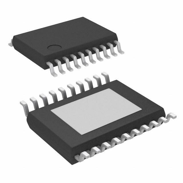


 工商网监
湘ICP备2023018690号
工商网监
湘ICP备2023018690号
