THS7316
www.ti.com
SLOS521A – MARCH 2007 – REVISED JANUARY 2008
3-Channel HDTV Video Amplifier With 5th-Order Filters and 6-dB Gain
FEATURES
1
•
•
•
•
•
•
•
•
•
DESCRIPTION
3 HDTV Video Amplifiers for Y'P'BP'R 720p and
1080i, G'B'R' (R'G'B'), VGA/SVGA/XGA
Integrated Low-Pass Filters
– 5th-Order 36-MHz (–3 dB) Butterworth Filter
– –1 dB Passband Bandwidth at 31 MHz
– 30 dB Attenuation at 74 MHz
Versatile Input Biasing
– DC-Coupled With 140-mV Input Shift
– AC-Coupled with Sync-Tip Clamp
– Allows AC-Coupled With Biasing
Built-in 6-dB Gain (2V/V)
3-V to 5-V Single Supply Operation
Rail-to-Rail Output:
– Output Swings Within 100 mV From the
Rails Allowing AC or DC Output Coupling
– Supports Driving 2 Lines per Channel
Low 18.3-mA at 3.3-V Total Quiescent Current
Low Differential Gain/Phase of 0.1% / 0.1°
SOIC-8 Package
Fabricated using the Silicon-Germanium (SiGe)
BiCom-III process, the THS7316 is a low power
single-supply 3-V to 5-V, 3-channel integrated video
buffer. It incorporates a 5th-order modified
Butterworth filter which is useful as a DAC
reconstruction filter or an ADC anti-aliasing filter. The
36-MHz filter is a perfect choice for HDTV video
which includes Y'P'BP'R 720p/1080i, G'B'R' (R'G'B'),
and VGA/SVGA/XGA signals.
As part of the THS7316 flexibility, the input can be
configured for ac or dc coupled inputs. The DC +
140-mV input offset shift to allow for a full sync
dynamic range at the output with 0-V input. The AC
coupled modes include a transparent sync-tip clamp
option for signals with sync such as Y’ or Green with
sync. AC-coupled biasing for P’B/P’R/Non-sync
channels can be achieved by adding an external
resistor.
The THS7316 is the perfect choice for all output
buffer applications. Its rail-to-rail output stage with
6-dB gain allows for both ac and dc line driving. The
ability to drive 2 video lines per channel, or 75-Ω
loads, allows for maximum flexibility as a video line
driver. The 18.3-mA total quiescent current makes it
an excellent choice for USB powered, portable, or
other power sensitive video applications.
APPLICATIONS
•
•
•
Set Top Box Output Video Buffering
PVR/DVDR Output Buffering
USB/Portable Low Power Video Buffering
The THS7316 is available in a small SOIC-8 package
that is RoHS compliant.
3.3 V
Y’ / G’ Out
75 W
DAC/
Encoder
75 W
Y’ / G’
THS7316
R
HDTV
720p/1080i
Y’P’BP’R
G’B’R’
VGA
SVGA
XGA
P’B / B’
R
P’R / R’
R
1
CH.1 IN
CH.1 OUT
8
2
CH.2 IN
CH.2 OUT
7
3
CH.3 IN
CH.3 OUT
6
4
VS+
GND
5
75 W
P’B / B’ Out
75 W
75 W
P’R/ R’ Out
3.3 V
75 W
Figure 1. 3.3-V Single-Supply DC-Input/DC Output Coupled Video Line Driver
1
Please be aware that an important notice concerning availability, standard warranty, and use in critical applications of
Texas Instruments semiconductor products and disclaimers thereto appears at the end of this data sheet.
PRODUCTION DATA information is current as of publication date.
Products conform to specifications per the terms of the Texas
Instruments standard warranty. Production processing does not
necessarily include testing of all parameters.
Copyright © 2007–2008, Texas Instruments Incorporated
�THS7316
www.ti.com
SLOS521A – MARCH 2007 – REVISED JANUARY 2008
This integrated circuit can be damaged by ESD. Texas Instruments recommends that all integrated circuits be handled with
appropriate precautions. Failure to observe proper handling and installation procedures can cause damage.
ESD damage can range from subtle performance degradation to complete device failure. Precision integrated circuits may be more
susceptible to damage because very small parametric changes could cause the device not to meet its published specifications.
PACKAGING/ORDERING INFORMATION
PACKAGE TYPE (1)
PACKAGED DEVICES
THS7316D
Rails, 75
SOIC-8
THS7316DR
(1)
TRANSPORT MEDIA, QUANTITY
Tape and Reel, 2500
For the most current package and ordering information, see the Package Option Addendum at the end of this document, or see the TI
Web site at www.ti.com.
ABSOLUTE MAXIMUM RATINGS
over operating free-air temperature range (unless otherwise noted)
(1)
VALUE
UNIT
5.5
V
Supply voltage, VS+ to GND
VI
Input voltage
IO
Output current
Continuous power dissipation
Maximum junction temperature, any condition
Maximum junction temperature, continuous operation, long term reliability (3)
Tstg
Storage temperature range
(2)
(3)
mA
See Dissipation Rating Table
TJ
(1)
V
±90
150
°C
125
°C
–65 to 150
°C
(2)
TJ
ESD ratings
–0.4 V to VS+
HBM
2000
CDM
1500
MM
200
V
Stresses above those listed under absolute maximum ratings may cause permanent damage to the device. These are stress ratings
only and functional operation of the device at these or any other conditions beyond those indicated under recommended operating
conditions is not implied. Exposure to absolute maximum rated conditions for extended periods may degrade device reliability.
The absolute maximum junction temperature under any condition is limited by the constraints of the silicon process.
The absolute maximum junction temperature for continuous operation is limited by the package constraints. Operation above this
temperature may result in reduced reliability and/or lifetime of the device.
DISSIPATION RATINGS
(1)
(2)
PACKAGE
θJC
(°C/W)
θJA
(°C/W)
SOIC-8 (D)
16.8
130 (2)
POWER RATING (1)
(TJ = 125°C)
TA = 25°C
TA = 85°C
769 mW
308 mW
Power rating is determined with a junction temperature of 125°C. This is the point where performance starts to degrade and long-term
reliability starts to be reduced. Thermal management of the final PCB should strive to keep the junction temperature at or below 125°C
for best performance and reliability.
This data was taken with the JEDEC High-K test PCB. For the JEDEC low-K test PCB, the θJA is 196°C/W.
RECOMMENDED OPERATING CONDITIONS
VS+
Supply voltage
TA
Ambient temperature
2
Submit Documentation Feedback
MIN
MAX
3
5
UNIT
V
–40
85
°C
Copyright © 2007–2008, Texas Instruments Incorporated
Product Folder Link(s) :THS7316
�THS7316
www.ti.com
SLOS521A – MARCH 2007 – REVISED JANUARY 2008
FUNCTIONAL DIAGRAM
+Vs
140 mV
Level
Shift
+
gm
Channel 1
Input
LPF
5-Pole
36-MHz
Sync-Tip
Clamp
(DC Restore)
800 kW
6dB
Channel 1
Output
6dB
Channel 2
Output
6dB
Channel 3
Output
+Vs
140 mV
Level
Shift
+
gm
Channel 2
Input
LPF
5-Pole
36-MHz
Sync-Tip
Clamp
(DC Restore)
800 kW
+Vs
140 mV
Level
Shift
+
gm
Channel 3
Input
Sync-Tip
Clamp
(DC Restore)
800 kW
LPF
5-Pole
36-MHz
3 V to 5 V
PIN CONFIGURATION
SOIC-8 (D)
(TOP VIEW)
THS7316
CH.1 IN 1
8
CH.1 OUT
CH.2 IN 2
7
CH.2 OUT
CH.3 IN 3
6
CH.3 OUT
VS+ 4
5
GND
TERMINAL FUNCTIONS
TERMINAL
NAME
NO. SOIC-8
I/O
DESCRIPTION
CH. 1 – INPUT
1
I
Video Input – Channel 1
CH. 2 – INPUT
2
I
Video Input – Channel 2
CH. 3 – INPUT
3
I
Video Input – Channel 3
+Vs
4
I
Positive Power Supply Pin – connect to 3 V to 5 V.
GND
5
I
Ground Pin for all internal circuitry.
CH. 3 – OUTPUT
6
O
Video Output – Channel 3
CH. 2 – OUTPUT
7
O
Video Output – Channel 2
CH. 1 – OUTPUT
8
O
Video Output – Channel 1
Submit Documentation Feedback
Copyright © 2007–2008, Texas Instruments Incorporated
Product Folder Link(s) :THS7316
3
�THS7316
www.ti.com
SLOS521A – MARCH 2007 – REVISED JANUARY 2008
ELECTRICAL CHARACTERISTICS VS+ = 3.3 V:
RL = 150 Ω to GND – Reference Figure 2 and Figure 3 (unless otherwise noted)
TYP
PARAMETER
TEST CONDITIONS
OVER TEMPERATURE
25°C
25°C
0°C to
70°C
–40°C to
85°C
UNITS
MIN/
MAX/
TYP
36
31/43
30/44
30/44
MHz
Min/Max
36
31/43
30/44
30/44
MHz
Min/Max
AC PERFORMANCE
Small-signal bandwidth (–3dB)
Large-signal bandwidth (–3dB)
VO – 0.2 VPP
VO – 2 VPP
(1)
(1)
–1 dB Passband bandwidth
Attenuation
With respect to 100 kHz
31
f = 27 MHz (2)
f = 74 MHz (2)
MHz
Typ
Min/Max
0.3
–0.3/2.4
–0.35/2.4
–0.4/2.6
dB
30
20
19
19
dB
Min
Group delay
f = 100 kHz
16.2
ns
Typ
Group delay variation
with respect to 100 kHz
f = 27 MHz
5.4
ns
Typ
0.3
ns
Typ
Differential gain
NTSC / PAL
0.1 /
0.15%
Differential phase
NTSC / PAL
0.1 / 0.1
°
Typ
Total harmonic distortion
f = 1 MHz; VO = 2 VPP
–70
dB
Typ
Signal to noise ratio
No Weighting, 100 kHz to 37.5 MHz
67
dB
Typ
Channel-to-channel crosstalk
f = 1 MHz
–61
dB
Typ
dB
Min/Max
Ω
Typ
Channel-to-channel delay
AC Gain – All channels
Output Impedance
6
f = 10 MHz
Typ
5.7/6.3
5.65/6.35
5.65/6.35
0.5
DC PERFORMANCE
Biased output voltage
VI = 0 V
Input voltage range
DC input, limited by output
Sync tip clamp charge current
VI = –0.1 V
285
Input resistance
Input capacitance
mV
Min/Max
–0.1/1.46
210/370
200/380
190/390
V
Typ
360
µA
Typ
800
kΩ
Typ
2
pF
Typ
V
Typ
OUTPUT CHARACTERISTICS
RL = 150 Ω to 1.65V
3.15
RL = 150 Ω to GND
3.1
RL = 75 Ω to 1.65V
V
Min
3.1
V
Typ
RL = 75 Ω to GND
3.0
V
Typ
RL = 150 Ω to 1.65V (VI = –0.15 V)
0.14
V
Typ
RL = 150 Ω to GND (VI = –0.15 V)
0.08
V
Max
RL = 75 Ω to 1.65V (VI = –0.15 V)
0.3
V
Typ
RL = 75 Ω to GND (VI = –0.15 V)
0.1
V
Typ
Output current (sourcing)
RL = 10 Ω to 1.65V
80
mA
Typ
Output current (sinking)
RL = 10 Ω to 1.65V
70
mA
Typ
Max
High output voltage swing
Low output voltage swing
2.85
0.17
2.75
0.2
2.75
0.21
POWER SUPPLY
Maximum operating voltage
3.3
5.5
5.5
5.5
V
Minimum operating voltage
3.3
2.85
2.85
2.85
V
Min
Max
Maximum quiescent current
VI = 0 V
18.3
22.5
23
23.4
mA
Minimum quiescent current
VI = 0 V
18.3
14
13.6
13.1
mA
Min
dB
Typ
Power Supply Rejection (+PSRR)
(1)
(2)
4
52
The Min/Max values listed for this specification are specified by design and characterization only.
3.3-V Supply Filter specifications are specified by 100% testing at 5-V supply along with design and characterization only.
Submit Documentation Feedback
Copyright © 2007–2008, Texas Instruments Incorporated
Product Folder Link(s) :THS7316
�THS7316
www.ti.com
SLOS521A – MARCH 2007 – REVISED JANUARY 2008
ELECTRICAL CHARACTERISTICS VS+ = 5 V:
RL = 150Ω to GND – Reference Figure 2 and Figure 3 (unless otherwise noted)
TYP
PARAMETER
TEST CONDITIONS
OVER TEMPERATURE
25°C
25°C
0°C to
70°C
–40°C to
85°C
UNITS
MIN/
MAX/
TYP
36
31/43
30/44
30/44
MHz
Min/Max
36
31/43
30/44
30/44
MHz
Min/Max
AC PERFORMANCE
Small-signal bandwidth (–3dB)
Large-signal bandwidth (–3dB)
VO – 0.2 VPP
VO – 2 VPP
(1)
(1)
–1dB Passband bandwidth
Attenuation
With respect to 100 kHz
31
f = 27 MHz
MHz
Typ
Min/Max
0.3
–0.3/2.4
–0.35/2.5
–0.4/2.6
dB
20
19
19
f = 74 MHz
30
dB
Min
Group delay
f = 100 kHz
16.1
ns
Typ
Group delay variation
with respect to 100kHz
f = 27 MHz
5.4
ns
Typ
0.3
ns
Typ
Differential gain
NTSC / PAL
0.1 /
0.15%
Differential phase
NTSC / PAL
0.1 / 0.1
°
Typ
Total harmonic distortion
f = 1 MHz; VO = 2 VPP
–70
dB
Typ
Signal to noise ratio
No Weighting, 100 kHz to 37.5 MHz
67
dB
Typ
Channel-to-channel crosstalk
f = 1 MHz
–62
dB
Typ
dB
Min/Max
Ω
Typ
Channel-to-channel delay
AC Gain – All channels
Output Impedance
6
f = 10 MHz
Typ
5.7/6.3
5.65/6.35
5.65/6.35
0.5
DC PERFORMANCE
Biased output voltage
VI = 0 V
Input voltage range
Limited by output
Sync tip clamp charge current
VI = –0.1 V
290
Input resistance
Input capacitance
mV
Min/Max
–0.1/2.3
210/370
200/380
190/390
V
Typ
380
µA
Typ
800
kΩ
Typ
2
pF
Typ
V
Typ
OUTPUT CHARACTERISTICS
RL = 150 Ω to 2.5V
4.85
RL = 150 Ω to GND
4.7
RL = 75 Ω to 2.5V
V
Min
4.7
V
Typ
RL = 75 Ω to GND
4.5
V
Typ
RL = 150 Ω to 2.5V (VI = –0.15 V)
0.19
V
Typ
RL = 150 Ω to GND (VI = –0.15 V)
0.09
V
Max
RL = 75 Ω to 2.5V (VI = –0.15 V)
0.35
V
Typ
RL = 75 Ω to GND (VI = –0.15 V)
0.1
V
Typ
Output current (sourcing)
RL = 10 Ω to 2.5 V
90
mA
Typ
Output current (sinking)
RL = 10 Ω to 2.5 V
85
mA
Typ
Max
High output voltage swing
Low output voltage swing
4.2
0.23
4.1
0.26
4.1
0.27
POWER SUPPLY
Maximum operating voltage
5
5.5
5.5
5.5
V
Minimum operating voltage
5
2.85
2.85
2.85
V
Min
Max
Maximum quiescent current
VI = 0 V
19.3
23
25
26
mA
Minimum quiescent current
VI = 0 V
19.3
14.7
14.2
13.8
mA
Min
dB
Typ
Power Supply Rejection (+PSRR)
(1)
52
The Min/Max values listed for this specification are specified by design and characterization only.
Submit Documentation Feedback
Copyright © 2007–2008, Texas Instruments Incorporated
Product Folder Link(s) :THS7316
5
�THS7316
www.ti.com
SLOS521A – MARCH 2007 – REVISED JANUARY 2008
DUT
R TERM
RSOURCE
R LOAD
R TERM
1 CH.1 IN
CH.1 OUT
8
2 CH.2 IN
CH.2 OUT
7
3 CH.3 IN
CH.3 OUT
6
GND
5
4 VS +
R LOAD
0.1 mF
VSOURCE
R LOAD
R TERM
+
100 mF
+VS
Figure 2. DC Coupled Input and Output Test Circuit
470 mF
+
C IN
DUT
R LOAD
RTERM
CIN
RSOURCE
RTERM
CIN
1
CH.1 IN
CH.1 OUT
8
2
CH.2 IN
CH.2 OUT
7
3
CH.3 IN
CH.3 OUT
6
4
VS +
GND
5
0.1 mF
VSOURCE
0.1 mF
470 mF
+
R LOAD
0.1 mF
470 mF
+
RTERM
RLOAD
+
+VS
100 mF
0.1 mF
Figure 3. AC Coupled Input and Output Test Circuit
6
Submit Documentation Feedback
Copyright © 2007–2008, Texas Instruments Incorporated
Product Folder Link(s) :THS7316
�THS7316
www.ti.com
SLOS521A – MARCH 2007 – REVISED JANUARY 2008
TYPICAL CHARACTERISTICS
SMALL-SIGNAL GAIN vs FREQUENCY
PHASE vs FREQUENCY
45
10
0
−45
−10
−90
RL = 150 W || 13 pF
Phase − o
Small-Signal Gain − dB
0
−20
RL = 75 W || 13 pF
−30
−135
−180
−225
−40
VS = 3.3 V
VO - 200 mVPP
−270
VS = 3.3 V
VO = 200 mVPP
−50
−60
0.1
−315
1
10
100
RL = 150 W || 13 pF
−360
0.1
1k
1
10
f − Frequency − MHz
f − Frequency − MHz
Figure 4.
Figure 5.
SMALL-SIGNAL GAIN vs FREQUENCY
100
GROUP DELAY vs FREQUENCY
6.5
25
5.5
RL = 150 W || 13 pF
5.0
Group Delay − ns
Small-Signal Gain − dB
6.0
4.5
RL = 75 W || 13 pF
4.0
3.5
15
VS = 3.3 V
VO = 200 mVPP
VS = 3.3 V
VO = 200 mVPP
3.0
RL = 150 W || 13 pF
2.5
1
10
10
0.1
100
100
f − Frequency − MHz
Figure 7.
LARGE-SIGNAL FREQUENCY RESPONSE
SMALL-SIGNAL FREQUENCY RESPONSE vs
CAPACITIVE LOADING
10
0
0
−10
−20
VS = 3.3 V
Load = 150 W || 13 pF
VO = 0.2 VPP
−40
−50
−10
VS = 3.3 V
VO = 200 mVPP
−20
Load = 150 W || CL
−30
CL = 13 pF
−40
CL = 5 pF
−50
VO = 2 VPP
−60
CL = 20 pF
−60
1
10
Figure 6.
10
−30
1
f − Frequency − MHz
Small-Signal Gain − dB
Signal Gain − dB
20
10
100
1k
1
10
100
f − Frequency − MHz
f − Frequency − MHz
Figure 8.
Figure 9.
Submit Documentation Feedback
Copyright © 2007–2008, Texas Instruments Incorporated
Product Folder Link(s) :THS7316
1k
7
�THS7316
www.ti.com
SLOS521A – MARCH 2007 – REVISED JANUARY 2008
TYPICAL CHARACTERISTICS (continued)
2nd HARMONIC DISTORTION vs
OUTPUT VOLTAGE
-30
-40
-20
VS = 3.3 V
Load = 150 W || 13 pF
3rd Order Harmonic Distortion − dB
2nd Order Harmonic Distortion − dB
-20
3rd HARMONIC DISTORTION vs
OUTPUT VOLTAGE
F = 8 MHz
F = 16 MHz
-50
-60
-70
-80
F = 1 MHz
F = 4 MHz
-90
0.5
F = 2 MHz
1
1.5
2
2.5
VS = 3.3 V
-30
-40
-60
-70
F = 2 MHz
-80
-90
F = 1 MHz
1
Figure 11.
SMALL-SIGNAL GAIN vs FREQUENCY
0
Small-Signal Gain − dB
Small-Signal Gain − dB
VS = 3.3 V
VO = 1 VPP
Ch.1 < -> Ch.2
−70
Ch.2 < -> Ch.3
Ch.1 < -> Ch.3
−80
1
−10
RL = 150 W || 13 pF
−20
RL = 75 W || 13 pF
−30
−40
VS = 5 V
VO = 200 mVPP
−50
10
100
−60
0.1
1k
1
f − Frequency − MHz
Figure 12.
Figure 13.
PHASE vs FREQUENCY
0
6.0
Small-Signal Gain − dB
−45
Phase − o
−90
−135
−180
−225
8
100
1k
SMALL-SIGNAL GAIN vs FREQUENCY
6.5
−360
0.1
10
f − Frequency − MHz
45
−315
3
10
−60
−270
2.5
Figure 10.
RL = 150 W || 13 pF
−90
0.1
2
VO − Output Voltage − VPP
CROSSTALK vs FREQUENCY
−50
1.5
VO − Output Voltage − VPP
−30
−40
F = 4 MHz
F = 16 MHz
-50
-100
0.5
3
F = 8 MHz
Load = 150 W || 13 pF
VS = 5 V
VO - 200 mVPP
5.5
RL = 150 W || 13 pF
5.0
4.5
RL = 75 W || 13 pF
4.0
3.5
VS = 5 V
VO = 200 mVPP
3.0
RL = 150 W || 13 pF
2.5
1
10
100
1
10
f − Frequency − MHz
f − Frequency − MHz
Figure 14.
Figure 15.
Submit Documentation Feedback
100
Copyright © 2007–2008, Texas Instruments Incorporated
Product Folder Link(s) :THS7316
�THS7316
www.ti.com
SLOS521A – MARCH 2007 – REVISED JANUARY 2008
TYPICAL CHARACTERISTICS (continued)
GROUP DELAY vs FREQUENCY
LARGE-SIGNAL FREQUENCY RESPONSE
25
10
Signal Gain − dB
Group Delay − ns
0
20
15
VS = 5 V
VO = 200 mVPP
−10
−20
VS = 5 V
−30
Load = 150 W || 13 pF
VO = 0.2 VPP
−40
−50
VO = 2 VPP
RL = 150 W || 13 pF
−60
10
0.1
1
10
100
1
f − Frequency − MHz
Figure 17.
SMALL-SIGNAL FREQUENCY RESPONSE vs
CAPACITIVE LOADING
2nd HARMONIC DISTORTION vs
OUTPUT VOLTAGE
2nd Order Harmonic Distortion − dB
Small-Signal Gain − dB
0
−10
VS = 5 V
VO = 200 mVPP
Load = 150 W || CL
CL = 13 pF
−40
CL = 5 pF
−50
CL = 20 pF
−60
1
10
100
-30
VS = 5 V
-40
F = 16 MHz
-50
-60
-70
-80
F = 4 MHz
-90
0.5
1k
1
1.5
2
2.5
3
3.5
VO − Output Voltage − VPP
Figure 18.
Figure 19.
4
4.5
CROSSTALK vs FREQUENCY
−30
VS = 5 V
VS = 5 V
VO = 1 VPP
F = 8 MHz
Load = 150 W || 13 pF
Small-Signal Gain − dB
−40
-40
F = 4 MHz
F = 16 MHz
-50
-60
-70
F = 2 MHz
-80
RL = 150 W || 13 pF
−50
Ch.1 < -> Ch.2
−60
−70
Ch.2 < -> Ch.3
Ch.1 < -> Ch.3
−80
-90
-100
0.5
F = 1 MHz
F = 2 MHz
f − Frequency − MHz
-20
3rd Order Harmonic Distortion − dB
F = 8 MHz
Load = 150 W || 13 pF
3rd HARMONIC DISTORTION vs
OUTPUT VOLTAGE
-30
1k
Figure 16.
-20
−30
100
f − Frequency − MHz
10
−20
10
F = 1 MHz
1
1.5
2
2.5
3
3.5
4
4.5
−90
0.1
1
10
VO − Output Voltage − VPP
f − Frequency − MHz
Figure 20.
Figure 21.
100
Submit Documentation Feedback
Copyright © 2007–2008, Texas Instruments Incorporated
Product Folder Link(s) :THS7316
1k
9
�THS7316
www.ti.com
SLOS521A – MARCH 2007 – REVISED JANUARY 2008
TYPICAL CHARACTERISTICS (continued)
QUIESCENT CURRENT vs TEMPERATURE
VOLTAGE GAIN vs TEMPERATURE
6.1
19.5
6.08
VS = 5 V
AV − Voltage Gain − dB
IQ − Quiescent Current − mA
20
19
VS = 3.3 V
18.5
18
6.06
6.04
VS = 3.3 V
VS = 5 V
6.02
6
5.98
5.96
5.94
5.92
17.5
-40 -30 -20 -10 0
10 20 30 40
5.9
-40 -30 -20 -10 0
50 60 70 80 90
o
Figure 22.
Figure 23.
ATTENUATION at 27 MHz vs TEMPERATURE
ATTENUATION at 74 MHz vs TEMPERATURE
0.7
33
Attenuation at 74 MHz − dB
0.6
Attenuation at 27 MHz − dB
50 60 70 80 90
TA − Ambient Temperature − oC
TA − Ambient Temperature − C
VS = 5 V
0.5
0.4
0.3
0.2
0.1
0
-40 -30 -20 -10 0
10 20 30 40
50 60 70 80 90
32
VS = 5 V
31
30
29
28
27
-40 -30 -20 -10 0
TA − Ambient Temperature − oC
Figure 24.
10
10 20 30 40
10 20 30 40
50 60 70 80 90
TA − Ambient Temperature − oC
Figure 25.
Submit Documentation Feedback
Copyright © 2007–2008, Texas Instruments Incorporated
Product Folder Link(s) :THS7316
�THS7316
www.ti.com
SLOS521A – MARCH 2007 – REVISED JANUARY 2008
APPLICATION INFORMATION
The THS7316 is targeted for standard definition video output buffer applications. Although it can be used for
numerous other applications, the needs and requirements of the video signal is an important design parameter of
the THS7316. Built on the Silicon Germanium (SiGe) BiCom-3 process, the THS7316 incorporates many
features not typically found in integrated video parts while consuming low power.
The THS7316 has the following features:
• Single-Supply 3-V to 5-V operation with low total quiescent current of 18.3-mA at 3.3-V and 19.3-mA at 5-V.
• Input configuration accepting DC + Level shift, AC Sync-Tip Clamp.
• AC-Biasing is accomplished with the use of an external pull-up resistor to the positive power supply.
• 5th-Order Low Pass Filter for DAC reconstruction or ADC image rejection:
– 36-MHz for HDTV, Y'P'BP'R 720p/1080i, G'B'R' (R'G'B'), and Computer VGA/SVGA/XGA signals.
– Can also be used for SDTV (480i, 576i, CVBS, S-Video), and EDTV (480p and 576p) signals if desired.
• Internal fixed gain of 2 V/V (6 dB) buffer that can drive up to 2 video lines per channel with dc coupling or
traditional ac coupling.
• Signal flow-through configuration using an 8-pin SOIC package that complies with the latest (RoHS
compatible) and Green manufacturing requirements.
OPERATING VOLTAGE
The THS7316 is designed to operate from 3-V to 5-V over a –40°C to 85°C temperature range. The impact on
performance over the entire temperature range is negligible due to the implementation of thin film resistors and
high quality – low temperature coefficient capacitors.
The power supply pins should have a 0.1-µF to 0.01-µF capacitor placed as close as possible to these pins.
Failure to do so may result in the THS7316 outputs ringing or have an oscillation. Additionally, a large capacitor,
such as 22 µF to 100 µF, should be placed on the power supply line to minimize interference with 50/60 Hz line
frequencies.
INPUT VOLTAGE
The THS7316 input range allows for an input signal range from –0.3 V to about (Vs+ – 1.5 V). But, due to the
internal fixed gain of 2 V/V (6 dB) and the internal level shift of nominally 140-mV, the output is generally the
limiting factor for the allowable linear input range. For example, with a 5-V supply, the linear input range is from
–0.3 V to 3.5 V. However, due to the gain and level shift, the linear output range limits the allowable linear input
range to be from about –0.1 V to 2.3 V.
INPUT OVERVOLTAGE PROTECTION
The THS7316 is built using a high-speed complementary bipolar and CMOS process. The internal junction
breakdown voltages are low for these small geometry devices. These breakdowns are reflected in the Absolute
Maximum Ratings table. All input and output device pins are protected with internal ESD protection diodes to the
power supplies, as shown in Figure 26.
+ Vs
External
Input/
Output
Pin
Internal
Circuitry
Figure 26. Internal ESD Protection
Submit Documentation Feedback
Copyright © 2007–2008, Texas Instruments Incorporated
Product Folder Link(s) :THS7316
11
�THS7316
www.ti.com
SLOS521A – MARCH 2007 – REVISED JANUARY 2008
These diodes provide moderate protection to input overdrive voltages above and below the supplies as well. The
protection diodes can typically support 30-mA of continuous current when overdriven.
TYPICAL CONFIGURATION and VIDEO TERMINOLOGY
A typical application circuit using the THS7316 as a video buffer is shown in Figure 27. It shows a DAC (or
encoder such as the THS8200) driving the three input channels of the THS7316. Although these channels show
HDTV Y'P'BP'R (sometimes labeled Y'C'BC'R) signals of a 720p or 1080i system, they can also be G'B'R' (R'G'B')
signals or other variations.
Note that the Y' term is used for the luma channels throughout this document rather than the more common
luminance (Y) term. The reason is to account for the definition of luminance as stipulated by the CIE –
International Commission on Illumination. Video departs from true luminance since a nonlinear term, gamma, is
added to the true RGB signals to form R'G'B' signals. These R'G'B' signals are then used to mathematically
create luma (Y'). Thus luminance (Y) is not maintained providing a difference in terminology.
This rationale is also used for the chroma (C') term. Chroma is derived from the non-linear R'G'B' terms and thus
it is nonlinear. Chrominance (C) is derived from linear RGB giving the difference between chroma (C') and
chrominance (C). The color difference signals (P'B / P'R / U' / V') are also referenced this way to denote the
nonlinear (gamma corrected) signals.
R'G'B' (commonly mislabeled RGB) is also called G’B’R’ (again commonly mislabeled as GBR) in professional
video systems. The SMPTE component standard stipulates that the luma information is placed on the first
channel, the blue color difference is placed on the second channel, and the red color difference signal is placed
on the third channel. This is consistent with the Y'P'BP'R nomenclature. Because the luma channel (Y') carries the
sync information and the green channel (G') also carries the sync information, it makes logical sense that G' be
placed first in the system. Since the blue color difference channel (P'B) is next and the red color difference
channel (P'R) is last, then it also makes logical sense to place the B' signal on the second channel and the R'
signal on the third channel, respectively . Thus hardware compatibility is better achieved when using G'B'R'
rather than R'G'B'. Note that for many G'B'R' systems sync is embedded on all three channels, but may not
always be the case in all systems.
3.3 V
330 mF 75 W
+
DAC/
Encoder
75 W
Y’
THS7316
R
HDTV
720p/1080i
Y’P’BP’R
G’B’R’
VGA
SVGA
XGA
Y’ Out
P’B
R
1
CH.1 IN
CH.1 OUT
8
2
CH.2 IN
CH.2 OUT
7
3
CH.3 IN
CH.3 OUT
6
4
VS+
GND
5
P’R
0.1 mF
R
330 mF 75 W
+
P’B Out
75 W
330 mF
75 W
P’R Out
+
3 V to 5 V
75 W
22 mF
Figure 27. Typical HDTV Y'/P'B/P'R Inputs From DC-Coupled Encoder/DAC
With AC-Coupled Line Driving
12
Submit Documentation Feedback
Copyright © 2007–2008, Texas Instruments Incorporated
Product Folder Link(s) :THS7316
�THS7316
www.ti.com
SLOS521A – MARCH 2007 – REVISED JANUARY 2008
INPUT MODE OF OPERATION – DC
The inputs to the THS7316 allows for both ac-coupled and dc-coupled inputs. Many DACs or Video Encoders
can be dc connected to the THS7316. One of the drawbacks to dc coupling is when 0-V is applied to the input.
Although the input of the THS7316 allows for a 0-V input signal with no issues, the output swing of a traditional
amplifier cannot yield a 0-V signal resulting in possible clipping. This is true for any single-supply amplifier due to
the limitations of the output transistors. Both CMOS and bipolar transistors cannot go to 0-V while sinking
current. This trait of a transistor is also the same reason why the highest output voltage is always less than the
power supply voltage when sourcing current.
This output clipping can reduce the sync amplitudes (both horizontal and vertical sync amplitudes) on the video
signal. A problem occurs if the receiver of this video signal uses an AGC loop to account for losses in the
transmission line. Some video AGC circuits derive gain from the horizontal sync amplitude. If clipping occurs on
the sync amplitude, then the AGC circuit can increase the gain too much – resulting in too much amplitude gain
correction. This may result in a picture with an overly bright display with too much color saturation.
It is good engineering design practice to ensure saturation/clipping does not take place. Transistors always take
a finite amount of time to come out of saturation. This saturation could possibly result in timing delays or other
aberrations on the signals.
To eliminate saturation/clipping problems, the THS7316 has a dc + 140-mV input shift feature. This feature takes
the input voltage and adds an internal +140-mV shift to the signal. Since the THS7316 also has a gain of 6 dB (2
V/V), the resulting output with a 0-V applied input signal is about 280-mV. The THS7316 rail-to-rail output stage
can create this output level while connected to a typical video load. This ensures that no saturation / clipping of
the sync signals occur. This is a constant shift regardless of the input signal. For example, if a 1-V input is
applied, the output is at 2.28-V.
Because the internal gain is fixed at 6 dB, the gain dictates what the allowable linear input voltage range can be
without clipping concerns. For example, if the power supply is set to 3-V, the maximum output is about 2.9-V
while driving a significant amount of current. Thus, to avoid clipping, the allowable input is ((2.9 V / 2) – 0.14 V) =
1.31 V. This is true for up to the maximum recommended 5-V power supply that allows about a ((4.9V / 2) – 0.14
V) = 2.31 V input range while avoiding clipping on the output.
The input impedance of the THS7316 in this mode of operation is dictated by the internal 800-kΩ pull-down
resistor. This is shown in Figure 28. Note that the internal voltage shift does not appear at the input pin, only the
output pin.
+ Vs
Internal
Circuitry
Input
+
800 kW
-
140 mV Level
Shifter
Figure 28. Equivalent DC Input Mode Circuit
Submit Documentation Feedback
Copyright © 2007–2008, Texas Instruments Incorporated
Product Folder Link(s) :THS7316
13
�THS7316
www.ti.com
SLOS521A – MARCH 2007 – REVISED JANUARY 2008
INPUT MODE OF OPERATION – AC SYNC TIP CLAMP
Some video DACs or encoders are not referenced to ground but rather to the positive power supply. These
DACs typically only sink current rather than the more traditional current sourcing DAC where the resistor is
referenced to ground. The resulting video signals can be too high of a voltage for a dc-coupled video buffer to
function properly. To account for this scenario the THS7316 incorporates a sync-tip clamp circuit. This function
requires a capacitor (nominally 0.1 µF) to be in series with the input. Note, while the term sync-tip-clamp is used
throughout this document, it should be noted that the THS7316 is better termed as a dc-restoration circuit based
on how this function is performed. This circuit is an active clamp circuit and not a passive diode clamp function.
The input to the THS7316 has an internal control loop which sets the lowest input applied voltage to clamp at
ground (0-V). By setting the reference at 0-V, the THS7316 allows a dc-coupled input to also function. Hence,
the STC is considered transparent since it does not operate unless the input signal goes below ground. The
signal then goes through the same 140-mV level shifter resulting in an output voltage low level of 280-mV. If the
input signal tries to go below the 0-V, the internal control loop of the THS7316 will source up to 3-mA of current
to increase the input voltage level on the THS7316 input side of the coupling capacitor. As soon as the voltage
goes above the 0-V level, the loop stops sourcing current and becomes high impedance.
One of the concerns about the sync-tip-clamp level is how the clamp reacts to a sync edge that has
overshoot—common in VCR signals or reflections found in poor PCB layouts. Ideally the STC should not react to
the overshoot voltage of the input signal. Otherwise, this could result in clipping on the rest of the video signal as
it may raise the bias voltage too much.
To help minimize this input signal overshoot problem, the control loop in the THS7316 has an internal low-pass
filter as shown in Figure 29. This filter reduces the response time of the STC circuit. This delay is a function of
how far the voltage is below ground, but in general it is about a 80-ns delay. The effect of this filter is to slow
down the response of the control loop so as not to clamp on the input overshoot voltage, but rather the flat
portion of the sync signal.
As a result of this delay, the sync may have an apparent voltage shift. The amount of shift is dependant upon the
amount of droop in the signal as dictated by the input capacitor and the STC current flow. Because the sync is
primarily for timing purposes with syncing occurring on the edge of the sync signal, this shift is transparent in
most systems.
While this feature may not fully eliminate overshoot issues on the input signal for excessive overshoot and/or
ringing, the STC system should help minimize improper clamping levels. As an additional method to help
minimize this issue, an external capacitor (ex: 10 pF to 47 pF) to ground in parallel with the external termination
resistors can help filter overshoot problems.
It should be noted that this STC system is dynamic and does not rely upon timing in any way. It only depends on
the voltage appearing at the input pin at any given point in time. The STC filtering helps minimize level shift
problems associated with switching noises or very short spikes on the signal line. This helps ensure a very
robust STC system.
+Vs
+Vs
Comparator
STC LPF
Internal
Circuitry
+
Input
Pin
-
Input
+
0.1 mF
800 kW
-
140 mV Level
Shifter
Figure 29. Equivalent AC Sync Tip Clamp Input Circuit
When the AC Sync-Tip-Clamp (STC) operation is used, there must also be some finite amount of discharge bias
14
Submit Documentation Feedback
Copyright © 2007–2008, Texas Instruments Incorporated
Product Folder Link(s) :THS7316
�THS7316
www.ti.com
SLOS521A – MARCH 2007 – REVISED JANUARY 2008
current. As previously described, if the input signal goes below the 0-V clamp level, the internal loop of the
THS7316 will source current to increase the voltage appearing at the input pin. As the difference between the
signal level and the 0-V reference level increases, the amount of source current increases
proportionally—supplying up to 3-mA of current. Thus the time to re-establish the proper STC voltage can be
fast. If the difference is small, then the source current is also small to account for minor voltage droop.
But, what happens if the input signal goes above the 0-V input level? The problem is the video signal is always
above this level, and must not be altered in any way. But if the Sync level of the input signal is above this 0-V
level, then the internal discharge (sink) current will discharge the ac-coupled bias signal to the proper 0-V level.
This discharge current must not be large enough to alter the video signal appreciably, or picture quality issues
may arise. This is often seen by looking at the tilt (aka droop) of a constant luma signal being applied and looking
at the resulting output level. The associated change in luma level from the beginning of the video line to the end
of the video line is the amount of line tilt (droop).
If the discharge current is small, the amount of tilt is low which is good. But, the amount of time for the system to
capture the sync signal could be too long. This is also termed hum rejection. Hum arises from the ac line voltage
frequency of 50-Hz or 60-Hz. The value of the discharge current and the ac-coupling capacitor combine to dictate
the hum rejection and the amount of line tilt.
To allow for both dc-coupling and ac-coupling in the same part, the THS7316 incorporates an 800-kΩ resistor to
ground. Although a true constant current sink is preferred over a resistor, there are significant issues when the
voltage is near ground. This can cause the current sink transistor to saturate and cause potential problems with
the signal. This resistor is large enough as to not impact a dc-coupled DAC termination. For discharging an
ac-coupled source, Ohm’s Law is used. If the video signal is 1 V, then there is 1 V / 800 kΩ = 1.25-µA of
discharge current. If more hum rejection is desired or there is a loss of sync occurring, then decrease the 0.1-µF
input coupling capacitor. A decrease from 0.1 µF to 0.047 µF increases the hum rejection by a factor of 2.1.
Alternatively an external pull-down resistor to ground may be added which decreases the overall resistance, and
ultimately increases the discharge current.
To ensure proper stability of the AC STC control loop, the source impedance must be less than 1-kΩ with the
input capacitor in place. Otherwise, there is a possibility of the control loop to ring and this ringing may appear on
the output of the THS7316. Because most DACs or encoders use resistors to establish the voltage, which are
typically less than 300-Ω, then meeting the 1 MHz) signals with much
lower impedance than the large capacitors.
Although it is common to use the same capacitor values for all the video lines, the frequency bandwidth of the
chroma signal in a S-Video system are not required to go as low – or as high of a frequency – as the luma
channels. Thus the capacitor values of the chroma line(s) can be smaller – such as 0.1-µF.
330 mf
(Note A) 75 W
Y’
Out 1
+
75 W
330 mf
(Note A) 75 W
3.3 V
3.3 V
P’ B
3.3 V
3.01 MW
0.1 mF
R
HDTV
720p/1080i
Y’P’BP’R
G’B’R’
75 W
0.1 mF
330 mf
Y’
DAC/
Encoder
+
3.3 V
R
3.3 V
R
Y’
Out 2
+
CH.1 IN
CH.1 OUT
8
2
CH.2 IN
CH.2 OUT
7
3
CH.3 IN
CH.3 OUT
6
4
VS+
GND
5
1
3.3 V
3.01 MW
0.1 mF
(Note A)
THS7316
P’R
75 W
P’ B
Out 1
75 W
330 mf
(Note A) 75 W
P’B
Out 2
+
75 W
0.1 mF
330 mf
+
3.3 V
(Note A) 75 W
P’ R
Out 1
+
22 mF
75 W
330 mf
(Note A) 75 W
P’R
Out 2
+
75 W
A.
Due to the high frequency content of the video signal, it is recommended, but not required, to add a 0.1-µF or 0.01-µF
capacitor in parallel with these large capacitors.
B.
Current sinking DAC / Encoder shown. See the application notes.
Figure 32. Typical 480i/576i Y'P'BP'R AC-Input System Driving 2 AC-Coupled Video Lines
18
Submit Documentation Feedback
Copyright © 2007–2008, Texas Instruments Incorporated
Product Folder Link(s) :THS7316
�THS7316
www.ti.com
SLOS521A – MARCH 2007 – REVISED JANUARY 2008
LOW PASS FILTER
Each channel of the THS7316 incorporates a 5th-Order Low Pass Filter. These video reconstruction filters
minimize DAC images from being passed onto the video receiver. Depending on the receiver design, failure to
eliminate these DAC images can cause picture quality problems due to aliasing of the ADC. Another benefit of
the filter is to smooth out aberrations in the signal which some DACs can have if their own internal filtering is not
good. This helps with picture quality and helps insure the signal meets video bandwidth requirements.
Each filter in the THS7316 is associated with a Butterworth characteristic. The benefit of the Butterworth
response is that the frequency response is flat with a relatively steep initial attenuation at the corner frequency.
The problem is that the group delay rises near the corner frequency. Group delay is defined as the change in
phase (radians/second) divided by a change in frequency. An increase in group delay corresponds to a time
domain pulse response that has overshoot and some possible ringing associated with the overshoot.
The use of other type of filters, such as elliptic or chebyshev, are not recommended for video applications due to
their very large group delay variations near the corner frequency resulting in significant overshoot and ringing.
While these elliptic or chebyshev filters may help meet the video standard specifications with respect to
amplitude attenuation, their group delay is beyond the standard specifications. Coupled with the fact that video
can go from a white pixel to a black pixel over and over again, ringing can occur. Ringing typically causes a
display to have ghosting or fuzziness appear on the edges of a sharp transition. However, a Bessel filter has an
ideal group delay response, but the rate of attenuation is typically too low for acceptable image rejection. Thus
the Butterworth filter is a respectable compromise for both attenuation and group delay.
The THS7316 filters have a nominal corner (-3dB) frequency at 36-MHz and a –1 dB passband typically at
31-MHz. This 36-MHz filter is ideal for High Definition (HD) 720p and 1080i signals. For systems that oversample
significantly, the THS7316 can also be useful for Standard Definition (SD) NTSC and PAL signals such as
480i/576i Y'P'BP'R, Y'U'V', and broadcast G’B’R’ (R’G’B’) signals. It can also be useful with Enhanced Definition
(ED) signals including 480p/576p Y'P'BP'R, Y'U'V', broadcast G’B’R’ (R’G’B’) signals, and computer video signals.
The 36-MHz -3dB corner frequency was designed to allow a maximally flat video signal while achieving 30-dB of
attenuation at 74.25-MHz – a common sampling frequency between the DAC/ADC 2nd and 3rd Nyquist zones
found in many video systems. This is important because any signal appearing around this frequency can appear
in the baseband due to aliasing effects of an analog to digital converter found in a receiver. Keep in mind that
DAC images do not stop at 74.25 MHz, they continue around the sampling frequencies of 148.5 MHz,
222.75-MHz, 297-MHz, etc. Because of these multiple images that an ADC can fold down into the baseband
signal, the low pass filter must also eliminate these higher order images. The THS7316 has over 50-dB
attenuation at 148.5-MHz, over 50-dB attenuation at 222.75-MHz, and about 55-dB attenuation at 297-MHz.
Attenuation to 1-GHz is at least 36-dB which makes sure that images do not effect the desired video baseband
signal.
The 36-MHz filter frequency was chosen to account for process variations in the THS7316. To ensure the
required video frequencies are not affected, the filter corner frequency must be high enough to allow component
variations. The other consideration is the attenuation must be large enough to ensure the anti-aliasing /
reconstruction filtering is enough to meet the system demands. Thus, the filter frequencies were not arbitrarily
selected.
Submit Documentation Feedback
Copyright © 2007–2008, Texas Instruments Incorporated
Product Folder Link(s) :THS7316
19
�THS7316
www.ti.com
SLOS521A – MARCH 2007 – REVISED JANUARY 2008
BENEFITS OVER PASSIVE FILTERING
Two key benefits of using an integrated filter system, such as the THS7316, over a passive system is PCB area
and filter variations. The small SOIC-8 package (3-video channels) is much smaller over a passive RLC network,
especially a 5-pole passive network. Additionally, inductors have at best ±10% tolerances (normally ±15% to
±20% is common) and capacitors typically have ±10% tolerances. Using a Monte Carlo analysis shows that the
filter corner frequency (–3 dB), flatness (–1 dB), Q factor (or peaking), and channel-to-channel delay has wide
variations. This can lead to potential performance and quality issues in mass-production environments. The
THS7316 solves most of these problems by using the corner frequency as essentially the only variable.
One concern about an active filter in an integrated circuit is the variation of the filter characteristics when the
ambient temperature and the subsequent die temperature changes. To minimize temperature effects, the
THS7316 uses low temperature coefficient resistors and high quality – low temperature coefficient capacitors
found in the BiCom-3 process. The filters have been specified by design to account for process variations and
temperature variations to maintain proper filter characteristics. This maintains a low channel-to-channel time
delay which is required for proper video signal performance.
Another benefit of a THS7316 over a passive RLC filter are the input and output impedances. The input
impedance presented to the DAC varies significantly with a passive network and may cause voltage variations
over frequency. The THS7316 input impedance is 800 kΩ and only the 2-pF input capacitance plus the PCB
trace capacitance impacting the input impedance. As such, the voltage variation appearing at the DAC output is
better controlled with the THS7316.
On the output side of the filter, a passive filter will again have a impedance variation over frequency. The
THS7316 is an op-amp which approximates an ideal voltage source. A voltage source is desirable because the
output impedance is very low and can source and sink current. To properly match the transmission line
characteristic impedance of a video line, a 75-Ω series resistor is placed on the output. To minimize reflections
and to maintain a good return loss, this output impedance must maintain a 75-Ω impedance. A passive filter
impedance variation is not specified while the THS7316 has approximately 0.5-Ω of output impedance at
10 MHz. Thus, the system is matched better with a THS7316 compared to a passive filter.
One last benefit of the THS7316 over a passive filter is power dissipation. A DAC driving a video line must be
able to drive a 37.5-Ω load - the receiver 75-Ω resistor and the 75-Ω impedance matching resistor next to the
DAC to maintain the source impedance requirement. This forces the DAC to drive at least 1.25-V peak (100%
Saturation CVBS) / 37.5 Ω = 33.3 mA. A DAC is a current steering element and this amount of current flows
internally to the DAC even if the output is 0-V. Thus, power dissipation in the DAC may be high - especially when
6-channels are being driven. Using the THS7316, with a high input impedance and the capability to drive up to
2-video lines per channel, can reduce the DAC power dissipation significantly. This is because the resistance the
DAC is driving can be substantially increased. It is common to set this in a DAC by a current setting resistor on
the DAC. Thus, the resistance can be 300-Ω or more - substantially reducing the current drive demands from the
DAC and saving substantial amount of power. For example, a 3.3-V 6-Channel DAC dissipates 660 mW just for
the steering current capability (6 ch x 33.3 mA x 3.3 V) if it needs to drive 37.5-Ω load. With a 300-Ω load, the
DAC power dissipation due to current steering current would only be 82.5 mW (6 ch X 4.16 mA X 3.3 V).
20
Submit Documentation Feedback
Copyright © 2007–2008, Texas Instruments Incorporated
Product Folder Link(s) :THS7316
�THS7316
www.ti.com
SLOS521A – MARCH 2007 – REVISED JANUARY 2008
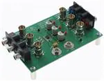
EVALUATION MODULE
To evaluate the THS7316, an evaluation module (EVM) is available. This allows for testing of the THS7316 in
many different systems. Inputs and outputs include RCA connectors for consumer grade interconnections, or
BNC connectors for higher level lab grade connections. Several unpopulated component pads are found on the
EVM to allow for different input and output configurations as dictated by the user.
+
Figure 33 shows the schematic of the THS7316 EVM. Figure 34 and Figure 35 shows the top layer and bottom
layer of the EVM which incorporates standard high-speed layout practices. The bill of materials is shown in
Table 1 as supplied from Texas Instruments.
+
+
+
Figure 33. THS7316D EVM
Submit Documentation Feedback
Copyright © 2007–2008, Texas Instruments Incorporated
Product Folder Link(s) :THS7316
21
�THS7316
www.ti.com
SLOS521A – MARCH 2007 – REVISED JANUARY 2008
Figure 34. Top View
Figure 35. Bottom View
22
Submit Documentation Feedback
Copyright © 2007–2008, Texas Instruments Incorporated
Product Folder Link(s) :THS7316
�THS7316
www.ti.com
SLOS521A – MARCH 2007 – REVISED JANUARY 2008
Bill of Materials
Table 1. THS7316D EVM
ITEM
REF DES
QTY
DESCRIPTION
SMD SIZE
1
FB1
1
BEAD, FERRITE, 2.5A, 330 OHM
2
C16
1
CAP, 100µF, TAN, 10V, 10%, LO ESR
3
C17, C18, C19
3
OPEN
0603
4
C15
1
CAP, 0.1µF, CERAMIC, 16V, X7R
0603
5
C1, C2, C3, C12,
C13, C14
6
OPEN
0805
6
C5
1
CAP, 0.01µF, CERAMIC, 100V, X7R
7
C7, C9, C11
3
8
C4
9
MANUFACTURER PART
NUMBER
DISTRIBUTOR PART
NUMBER
(TDK) MPZ2012S331A
(DIGI-KEY)
445-1569-1-ND
(AVX)
TPSC107K010R0100
(DIGI-KEY)
478-1765-1-ND
(AVX) 0603YC104KAT2A
(GARRETT)
0603YC104KAT2A
0805
(AVX) 08051C103KAT2A
(DIGI-KEY)
478-1358-1-ND
CAP, 0.1µF, CERAMIC, 50V, X7R
0805
(AVX) 08055C104KAT2A
(DIGI-KEY)
478-1395-1-ND
1
CAP, 1µF, CERAMIC, 16V, X7R
0805
(TDK) C2012X7R1C105K
(DIGI-KEY)
445-1358-1-ND
C6, C8, C10
3
CAP, ALUM, 470µF, 10V, 20%
(CORNELL)
AFK477M10F24B
(NEWARK) 97C7597
10
RX1, RX2, RX3,
RX4, RX5, RX6
6
OPEN
0603
11
R4, R5, R6, R7, R8,
R9, Z1, Z2, Z3
9
RESISTOR, 0 OHM
0805
(ROHM) MCR10EZHJ000
(DIGI-KEY)
RHM0.0ACT-ND
12
R1, R2, R3, R10,
R11, R12
6
RESISTOR, 75 OHM, 1/8W, 1%
0805
(ROHM) MCR10EZHF75.0
(DIGI-KEY)
RHM75.0CCT-ND
13
J9, J10
2
JACK, BANANA RECEPTANCE, 0.25"
DIA. HOLE
(SPC) 813
(NEWARK) 39N867
14
J1, J2, J3, J6, J7,
J8
6
CONNECTOR, BNC, JACK, 75 OHM
(AMPHENOL)
31-5329-72RFX
(NEWARK) 93F7554
15
J4, J5
2
CONNECTOR, RCA, JACK, R/A
(CUI) RCJ-32265
(DIGI-KEY) CP-1446-ND
16
TP1, TP2, TP3
3
TEST POINT, RED
(KEYSTONE) 5000
(DIGI-KEY) 5000K-ND
17
TP4, TP5
2
TEST POINT, BLACK
(KEYSTONE) 5001
(DIGI-KEY) 5001K-ND
18
U1
1
IC, THS7316
19
4
STANDOFF, 4-40 HEX, 0.625" LENGTH
(KEYSTONE) 1808
(NEWARK) 89F1934
20
4
SCREW, PHILLIPS, 4-40, .250"
(BF) PMS 440 0031 PH
(DIGI-KEY) H343-ND
21
1
BOARD, PRINTED CIRCUIT
EDGE # 6483761 REV. A
0805
C
F
D
(TI) THS7316D
EVALUATION BOARD/KIT IMPORTANT NOTICE
Texas Instruments (TI) provides the enclosed product(s) under the following conditions:
This evaluation board/kit is intended for use for ENGINEERING DEVELOPMENT, DEMONSTRATION, OR EVALUATION PURPOSES
ONLY and is not considered by TI to be a finished end-product fit for general consumer use. Persons handling the product(s) must have
electronics training and observe good engineering practice standards. As such, the goods being provided are not intended to be complete
in terms of required design-, marketing-, and/or manufacturing-related protective considerations, including product safety and environmental
measures typically found in end products that incorporate such semiconductor components or circuit boards. This evaluation board/kit does
not fall within the scope of the European Union directives regarding electromagnetic compatibility, restricted substances (RoHS), recycling
(WEEE), FCC, CE or UL, and therefore may not meet the technical requirements of these directives or other related directives.
Should this evaluation board/kit not meet the specifications indicated in the User’s Guide, the board/kit may be returned within 30 days from
the date of delivery for a full refund. THE FOREGOING WARRANTY IS THE EXCLUSIVE WARRANTY MADE BY SELLER TO BUYER
AND IS IN LIEU OF ALL OTHER WARRANTIES, EXPRESSED, IMPLIED, OR STATUTORY, INCLUDING ANY WARRANTY OF
MERCHANTABILITY OR FITNESS FOR ANY PARTICULAR PURPOSE.
The user assumes all responsibility and liability for proper and safe handling of the goods. Further, the user indemnifies TI from all claims
arising from the handling or use of the goods. Due to the open construction of the product, it is the user’s responsibility to take any and all
appropriate precautions with regard to electrostatic discharge.
EXCEPT TO THE EXTENT OF THE INDEMNITY SET FORTH ABOVE, NEITHER PARTY SHALL BE LIABLE TO THE OTHER FOR ANY
INDIRECT, SPECIAL, INCIDENTAL, OR CONSEQUENTIAL DAMAGES.
TI currently deals with a variety of customers for products, and therefore our arrangement with the user is not exclusive.
Submit Documentation Feedback
Copyright © 2007–2008, Texas Instruments Incorporated
Product Folder Link(s) :THS7316
23
�THS7316
www.ti.com
SLOS521A – MARCH 2007 – REVISED JANUARY 2008
EVALUATION BOARD/KIT IMPORTANT NOTICE (continued)
TI assumes no liability for applications assistance, customer product design, software performance, or infringement of patents or
services described herein.
Please read the User’s Guide and, specifically, the Warnings and Restrictions notice in the User’s Guide prior to handling the product. This
notice contains important safety information about temperatures and voltages. For additional information on TI’s environmental and/or
safety programs, please contact the TI application engineer or visit www.ti.com/esh.
No license is granted under any patent right or other intellectual property right of TI covering or relating to any machine, process, or
combination in which such TI products or services might be or are used.
FCC Warning
This evaluation board/kit is intended for use for ENGINEERING DEVELOPMENT, DEMONSTRATION, OR EVALUATION PURPOSES
ONLY and is not considered by TI to be a finished end-product fit for general consumer use. It generates, uses, and can radiate radio
frequency energy and has not been tested for compliance with the limits of computing devices pursuant to part 15 of FCC rules, which are
designed to provide reasonable protection against radio frequency interference. Operation of this equipment in other environments may
cause interference with radio communications, in which case the user at his own expense will be required to take whatever measures may
be required to correct this interference.
Mailing Address: Texas Instruments, Post Office Box 655303, Dallas, Texas 75265
Copyright 2008, Texas Instruments Incorporated
EVM WARNINGS AND RESTRICTIONS
It is important to operate this EVM within the input voltage range of 2.85 V to 5.5 V single supply and the output voltage range of 0 V to 5.5
V.
Exceeding the specified input range may cause unexpected operation and/or irreversible damage to the EVM. If there are questions
concerning the input range, please contact a TI field representative prior to connecting the input power.
Applying loads outside of the specified output range may result in unintended operation and/or possible permanent damage to the EVM.
Please consult the EVM User's Guide prior to connecting any load to the EVM output. If there is uncertainty as to the load specification,
please contact a TI field representative.
During normal operation, some circuit components may have case temperatures greater than 85C. The EVM is designed to operate
properly with certain components above 85C as long as the input and output ranges are maintained. These components include but are not
limited to linear regulators, switching transistors, pass transistors, and current sense resistors. These types of devices can be identified
using the EVM schematic located in the EVM User's Guide. When placing measurement probes near these devices during operation,
please be aware that these devices may be very warm to the touch.
Mailing Address: Texas Instruments, Post Office Box 655303, Dallas, Texas 75265
Copyright 2008, Texas Instruments Incorporated
24
Submit Documentation Feedback
Copyright © 2007–2008, Texas Instruments Incorporated
Product Folder Link(s) :THS7316
�PACKAGE OPTION ADDENDUM
www.ti.com
19-Oct-2022
PACKAGING INFORMATION
Orderable Device
Status
(1)
Package Type Package Pins Package
Drawing
Qty
Eco Plan
(2)
Lead finish/
Ball material
MSL Peak Temp
Op Temp (°C)
Device Marking
(3)
Samples
(4/5)
(6)
THS7316D
ACTIVE
SOIC
D
8
75
RoHS & Green
NIPDAU
Level-2-260C-1 YEAR
-40 to 85
7316
Samples
THS7316DG4
ACTIVE
SOIC
D
8
75
RoHS & Green
NIPDAU
Level-2-260C-1 YEAR
-40 to 85
7316
Samples
THS7316DR
ACTIVE
SOIC
D
8
2500
RoHS & Green
NIPDAU
Level-2-260C-1 YEAR
-40 to 85
7316
Samples
THS7316DRG4
ACTIVE
SOIC
D
8
2500
RoHS & Green
NIPDAU
Level-2-260C-1 YEAR
-40 to 85
7316
Samples
(1)
The marketing status values are defined as follows:
ACTIVE: Product device recommended for new designs.
LIFEBUY: TI has announced that the device will be discontinued, and a lifetime-buy period is in effect.
NRND: Not recommended for new designs. Device is in production to support existing customers, but TI does not recommend using this part in a new design.
PREVIEW: Device has been announced but is not in production. Samples may or may not be available.
OBSOLETE: TI has discontinued the production of the device.
(2)
RoHS: TI defines "RoHS" to mean semiconductor products that are compliant with the current EU RoHS requirements for all 10 RoHS substances, including the requirement that RoHS substance
do not exceed 0.1% by weight in homogeneous materials. Where designed to be soldered at high temperatures, "RoHS" products are suitable for use in specified lead-free processes. TI may
reference these types of products as "Pb-Free".
RoHS Exempt: TI defines "RoHS Exempt" to mean products that contain lead but are compliant with EU RoHS pursuant to a specific EU RoHS exemption.
Green: TI defines "Green" to mean the content of Chlorine (Cl) and Bromine (Br) based flame retardants meet JS709B low halogen requirements of