THS9001
www.ti.com
SLOS426C – NOVEMBER 2003 – REVISED DECEMBER 2013
50 MHz to 750 MHz CASCADEABLE AMPLIFIER
Check for Samples: THS9001
FEATURES
APPLICATIONS
•
•
1
2
•
•
•
High Dynamic Range
– OIP3 = 36 dBm
– NF < 4.5 dB
Single-Supply Voltage
High Speed
– VS = 3 V to 5 V
– IS = Adjustable
Input/Output Impedance
– 50 Ω
IF
–
–
–
–
Amplifiers
TDMA: GSM, IS-136, EDGE/UWE-136
CDMA: IS-95, UMTS, CDMA2000
Wireless Local Loops
Wireless LAN: IEEE802.11
DESCRIPTION
The THS9001 is a medium power, cascadeable, gain block optimized for high IF frequencies. The amplifier
incorporates internal impedance matching to 50 Ω, and achieves greater than 15-dB input, and output return loss
from 50 MHz to 350 MHz with VS = 5 V, R(BIAS) = 237 Ω, L(COL) = 470 nH. Design requires only 2 dc-blocking
capacitors, 1 power-supply bypass capacitor, 1 RF choke, and 1 bias resistor.
Function Block Diagram
VS
THS9001
IF(IN)
R(BIAS)
1
6
2
5
CIN
IF(OUT)
COUT
3
4
L(COL)
C(BYP)
VS
1
2
Please be aware that an important notice concerning availability, standard warranty, and use in critical applications of
Texas Instruments semiconductor products and disclaimers thereto appears at the end of this data sheet.
All trademarks are the property of their respective owners.
PRODUCTION DATA information is current as of publication date.
Products conform to specifications per the terms of the Texas
Instruments standard warranty. Production processing does not
necessarily include testing of all parameters.
Copyright © 2003–2013, Texas Instruments Incorporated
�THS9001
SLOS426C – NOVEMBER 2003 – REVISED DECEMBER 2013
www.ti.com
These devices have limited built-in ESD protection. The leads should be shorted together or the device placed in conductive foam
during storage or handling to prevent electrostatic damage to the MOS gates.
AVAILABLE OPTIONS
PACKAGED DEVICE
(1)
PACKAGE TYPE
THS9001DBVT
Tape and Reel, 250
SOT-23-6
THS9001DBVR
(1)
TRANSPORT MEDIA, QUANTITY
Tape and Reel, 3000
For the most current package and ordering information, see the Package Option Addendum at the end
of this document, or see the TI Web site at www.ti.com.
ABSOLUTE MAXIMUM RATINGS
Over operating free-air temperature (unless otherwise noted) (1)
UNIT
VSS
Supply voltage, GND to VS
VI
Input voltage
5.5
GND to VS
Continuous power dissipation
See Dissipation Rating
table
TJ
Maximum junction temperature
TJ
Maximum junction temperature, continuous operation, long term reliability
150°C
Tstg
Storage temperature
ESD Ratings
(2)
125°C
–65 to 150°C
:
(1)
(2)
HBM
2000
CDM
1500
MM
100
The absolute maximum ratings under any condition is limited by the constraints of the silicon process. Stresses above these ratings may
cause permanent damage. Exposure to absolute maximum conditions for extended periods may degrade device reliability. These are
stress ratings only, and functional operation of the device at these or any other conditions beyond those specified is not implied.
The maximum junction temperature for continuous operation is limited by package constraints. Operation above this temperature may
result in reduced reliability and/or lifetime of the device.
DISSIPATION RATING TABLE
(1)
(2)
POWER RATING (1)
PACKAGE
θJC
(°C/W)
θJA
(°C/W)
TA ≤ 25°C
TA = 85°C
DBV (2)
70.1
215
463 W
185 mW
Power rating is determined with a junction temperature of 125°C. Thermal management of the final PCB should strive to keep the
junction temperature at or below 125°C for best performance.
This data was taken using the JEDEC standard High-K test PCB.
RECOMMENDED OPERATING CONDITIONS
MIN
NOM
MAX
UNIT
VSS
Supply voltage
2.7
5
V
TA
Operating free-air temperature,
–40
85
°C
IS
Supply current
2
100
Submit Documentation Feedback
mA
Copyright © 2003–2013, Texas Instruments Incorporated
Product Folder Links: THS9001
�THS9001
www.ti.com
SLOS426C – NOVEMBER 2003 – REVISED DECEMBER 2013
ELECTRICAL CHARACTERISTICS
Typical Performance (VS = 5 V, R(BIAS) = 237 Ω, L(COL) = 470 nH) (unless otherwise noted)
PARAMETER
TEST CONDITIONS
Gain
OIP3
1-dB compression
Input return loss
Output return loss
Reverse isolation
Noise figure
MIN
TYP
f = 50 MHz
15.8
f = 350 MHz
15
f = 50 MHz
35
f = 350 MHz
37
f = 50 MHz
20.6
f = 350 MHz
20.6
f = 50 MHz
15.4
f = 350 MHz
16.6
f = 50 MHz
17
f = 350 MHz
15
f = 50 MHz
20.7
f = 350 MHz
20.7
f = 50 MHz
3.7
f = 350 MHz
4
MAX
UNITS
dB
dBm
dBm
dB
dB
dB
dB
PIN ASSIGNMENT
IF(IN)
1
6
GND
2
5
VS
3
4
BIAS
IF(OUT)
L(COL)
Terminal Functions
PIN NUMBERS
NAME
DESCRIPTION
1
IF(IN)
Signal input
2
GND
Negative power-supply input
3
VS
Positive power-supply input
4
L(COL)
Output transistor load inductor
5
IF(OUT)
Signal output
6
BIAS
Bias current input
SIMPLIFIED SCHEMATIC
VS
L(COL)
BIAS
IF(OUT)
IF(IN)
GND
Submit Documentation Feedback
Copyright © 2003–2013, Texas Instruments Incorporated
Product Folder Links: THS9001
3
�THS9001
SLOS426C – NOVEMBER 2003 – REVISED DECEMBER 2013
www.ti.com
TABLE OF GRAPHS
FIGURE
S21 Frequency response
1
S22 Frequency response
2
S11 Frequency response
3
S12 Frequency response
IS
4
S21
vs R(Bias)
5
Noise figure
vs Frequency
6
Supply current
vs R(Bias)
7
Output power vs Input power
8
Adjacent channel (ACPR) and Alternate channel
(AltCPR) protection ratios
vs Input power
9
OIP2
vs Frequency
10
OIP3
vs Frequency
11
S21 Frequency response
12
S22 Frequency response
13
S11 Frequency response
S12 Frequency response
14
vs Frequency
Noise figure
16
OIP2 vs Frequency
4
15
17
Output power
vs Input power
18
OIP3
vs Frequency
19
Submit Documentation Feedback
Copyright © 2003–2013, Texas Instruments Incorporated
Product Folder Links: THS9001
�THS9001
www.ti.com
SLOS426C – NOVEMBER 2003 – REVISED DECEMBER 2013
TYPICAL CHARACTERISTICS
S-Parameters of THS9000 as mounted on the EVM with VS = 5 V, R(BIAS) = 237 Ω, and L(COL) = 68 nH to 470 nH at room
temperature.
S21 FREQUENCY RESPONSE
L(COL) = 470 nH
16
S22 FREQUENCY RESPONSE
L(COL) = 100 nH
VS = 5 V,
R(BIAS) = 237 W
0
17
L(COL) = 220 nH
L(COL) = 330 nH
L(COL) = 68 nH
−5
S22 − dB
S21 − dB
15
14
13
L(COL) = 220 nH
L(COL) = 100 nH
12
−15
L(COL) = 68 nH
11
10
−10
L(COL) = 470 nH
VS = 5 V,
R(BIAS) = 237 W
1M
10 M
100 M
L(COL) = 330 nH
−20
1M
1G
S11 FREQUENCY RESPONSE
0
10 M
1G
S12 FREQUENCY RESPONSE
−15
VS = 5 V,
R(BIAS) = 237 W
L(COL) = 68 nH
−5
100 M
f − Frequency − Hz
Figure 2.
f − Frequency − Hz
Figure 1.
L(COL) = 470 nH
−20
L(COL) = 100 nH
L(COL) = 330 nH
L(COL) = 220 nH
−15
−20
−25
S12 − dB
S11 − dB
−10
L(COL) = 330 nH
−25
L(COL) = 220 nH
−30
L(COL) = 470 nH
L(COL) = 100 nH
−30
L(COL) = 68 nH
−35
VS = 5 V,
R(BIAS) = 237 W
−35
−40
1M
10 M
100 M
f − Frequency − Hz
Figure 3.
1G
−40
1M
10 M
100 M
f − Frequency − Hz
Figure 4.
Submit Documentation Feedback
Copyright © 2003–2013, Texas Instruments Incorporated
Product Folder Links: THS9001
1G
5
�THS9001
SLOS426C – NOVEMBER 2003 – REVISED DECEMBER 2013
www.ti.com
TYPICAl CHARACTERISTICS
S-Parameters of THS9000 as mounted on the EVM with VS = 3 V and 5 V, R(BIAS) = various, and L(COL) = 470 nH at room
temp.
S21
vs
R(BIAS)
NOISE FIGURE
vs
FREQUENCY
17
5
R(BIAS) = 56.2 W, VS = 3 V
4.75
16
VS = 5 V, IS = 99 mA
15
R(BIAS) = 237 W,
VS = 5 V
Noise Figure − dB
S21 − dB
VS = 5 V, IS = 75 mA
4.5
R(BIAS) = 97.7 W,VS = 3 V
14
R(BIAS) = 340 W, VS = 5 V
13
R(BIAS) = 549 W,VS = 5 V
VS = 3 V, IS = 94 mA
4.25
VS = 5 V, IS = 50 mA
4
VS = 3 V, IS = 49 mA
3.75
VS = 3 V, IS = 70 mA
12
3.5
R(BIAS) = 174 W, VS = 3 V
11
3.25
VS = 3 V to 5 V,
L(col) = 470 nH
10
3
50
1G
10 M
100 M
f − Frequency − Hz
Figure 5.
1M
22
180
20
PO − Output Power − dBm
160
I S − Supply Current − mA
350
450
500
OUTPUT POWER
vs
INPUT POWER
VS = 5 V, IS = 99 mA
21
140
120
VS = 5 V
100
80
VS = 3 V
60
250
f − Frequency − MHz
Figure 6.
SUPPLY CURRENT
vs
R(BIAS)
200
150
VS = 5 V, IS = 75 mA
19
VS = 5 V, IS = 50 mA
18
17
16
15
VS = 3 V, IS = 94 mA
14
VS = 3 V, IS = 70 mA
13
12
VS = 3 V, IS = 49 mA
40
11
f = 100 MHz
20
50
150
250
350
R(BIAS) − W
450
550
10
−6
Figure 7.
6
Submit Documentation Feedback
−4
−2
0
2
4
6
8
PI − Input Power − dBm
Figure 8.
10
12
14
Copyright © 2003–2013, Texas Instruments Incorporated
Product Folder Links: THS9001
�THS9001
www.ti.com
SLOS426C – NOVEMBER 2003 – REVISED DECEMBER 2013
TYPICAl CHARACTERISTICS (continued)
S-Parameters of THS9000 as mounted on the EVM with VS = 3 V and 5 V, R(BIAS) = various, and L(COL) = 470 nH at room
temp.
ADJACENT CHANNEL (ACPR) and ALTERNATE
CHANNEL (AltCPR) PROTECTION RATIOS
vs
INPUT POWER
WCDM Modulation, f = 1.8432 MHz, PAR = 10.4 dB
-20
VS = 5 V
ACPR
IS = 99 mA
-30
L(col) = 220 nH
OIP2
vs
FREQUENCY
50
L(COL) = 470 nH
VS = 3 V,
IS = 94 mA
48
VS = 5 V,
IS = 99 mA
44
OIP2 − dBm
Power Ratio− dB
46
AltCPR
-40
-50
42
VS = 5 V,
IS = 75 mA
40
-60
VS = 3 V,
IS = 70 mA
Source ACPR
38
-70
36
Source AltCPR
-80
-21
-18
-15
-12
-9
-6
-3
0
34
3
VS = 3 V,
IS = 49 mA
100
50
0
VS = 5 V,
IS = 50 mA
150
200
f − Frequency − MHz
Figure 10.
Input Power − dBM
Figure 9.
250
300
OIP3
vs
FREQUENCY
40
L(COL) = 470 nH
VS = 5 V, IS = 99 mA
38
OIP3 − dBm
36
VS = 5 V, IS = 75 mA
34
VS = 3 V, IS = 94 mA
VS = 3 V, IS = 70 mA
32
VS = 5 V, IS = 50 mA
30
28
VS = 3 V, IS = 49 mA
26
24
0
100
200
300
400
500
f − Frequency − MHz
Figure 11.
Submit Documentation Feedback
Copyright © 2003–2013, Texas Instruments Incorporated
Product Folder Links: THS9001
7
�THS9001
SLOS426C – NOVEMBER 2003 – REVISED DECEMBER 2013
www.ti.com
TYPICAL CHARACTERISTICS
THS9000 as mounted on the EVM with VS = 3 V and 5 V, R(BIAS) = 237 Ω, and L(COL) = 470 nH at –40°C, 25°C, and 85°C.
S21 FREQUENCY RESPONSE
S22 FREQUENCY RESPONSE
0
17
o
−45 C
VS = 5 V,
R(BIAS) = 237 W,
L(COL) = 470 nH
−2
16
−4
o
25 C
15
−6
85oC
S22 − dB
S21 − dB
−8
14
13
−10
o
85 C
−12
−14
12
o
25 C
−16
VS = 5 V,
R(BIAS) = 237 W,
L(col) = 470 nH
11
10
1M
10 M
100 M
f − Frequency − Hz
Figure 12.
−20
1G
1M
1G
VS = 5 V,
R(BIAS) = 237 W,
L(COL) = 470 nH
−20
−10
−45o C
−15
o
S12 − dB
S11 − dB
100 M
S12 FREQUENCY RESPONSE
−15
VS = 5 V,
R(BIAS) = 237 W,
L(COL) = 470 nH
−5
10 M
f − Frequency − Hz
Figure 13.
S11 FREQUENCY RESPONSE
0
−45 oC
−18
85 C
−20
−25
25o C
−25
o
85 C
−30
−30
−45 oC
−35
−40
−35
o
25 C
−45
1M
10 M
100 M
1G
−40
1M
f − Frequency − MHz
Figure 14.
8
10 M
100 M
1G
f − Frequency − Hz
Figure 15.
Submit Documentation Feedback
Copyright © 2003–2013, Texas Instruments Incorporated
Product Folder Links: THS9001
�THS9001
www.ti.com
SLOS426C – NOVEMBER 2003 – REVISED DECEMBER 2013
TYPICAL CHARACTERISTICS (continued)
THS9000 as mounted on the EVM with VS = 3 V and 5 V, R(BIAS) = 237 Ω, and L(COL) = 470 nH at –40°C, 25°C, and 85°C.
NOISE FIGURE
vs
FREQUENCY
6
OIP3
vs
FREQUENCY
48
VS = 5 V,
R(BIAS) = 237 W,
L(COL) = 470 nH
5.5
47
o
85 C
VS = 5 V,
R(BIAS) = 237 W,
L(COL) = 470 nH
o
−45 C
5
OIP2 − dBm
Noise Figure − dB
46
25 oC
4.5
45
25oC
o
85 C
44
43
4
42
o
−45 C
3.5
41
3
0
100
200
300
400
40
50
500
100
OUTPUT POWER
vs
INPUT POWER
250
300
OIP3
vs
FREQUENCY
40
22
VS = 5 V,
R(BIAS) = 237 W,
L(COL) = 470 nH
f = 100 MHz
o
25 C
39
20
VS = 5 V,
R(BIAS) = 237 W,
L(COL) = 470 nH
85oC
38
o
−45 C
25 oC
OIP3 − dBm
PO − Output Power − dBm
200
f − Frequency − MHz
Figure 17.
f − Frequency − MHz
Figure 16.
21
150
19
85oC
18
37
36
o
17
35
16
34
15
33
14
−2
0
2
4
6
8
PI − Input Power − dBm
Figure 18.
10
12
32
50
−45 C
100
150 200
250 300 350 400 450 500
f − Frequency − MHz
Figure 19.
Submit Documentation Feedback
Copyright © 2003–2013, Texas Instruments Incorporated
Product Folder Links: THS9001
9
�THS9001
SLOS426C – NOVEMBER 2003 – REVISED DECEMBER 2013
www.ti.com
TYPICAL CHARACTERISTICS
Table 1. S-Parameters Tables of THS9001 with EVM De-Embedded
VS = 5 V, R(BIAS) = 237 , L(COL) = 470 nH
S21
S11
S22
S12
Frequency
(MHz)
Gain (dB)
Phase (deg)
Gain (dB)
Phase (deg)
Gain (dB)
Phase (deg)
Gain (dB)
Phase (deg)
1.0
-3.5
-165.0
-2.3
-1.1
-2.6
174.8
-64.4
-121.7
10
5.0
11.7
-127.1
-1.5
-14.9
-2.8
140.4
-32.4
123.0
10.2
15.8
-150.1
-2.2
-42.3
-5.3
99.8
-23.6
79.5
19.7
16.3
-170.8
-6.6
-69.3
-10.7
64.5
-21.1
40.7
50.1
15.9
175.7
-16.2
-90.3
-16.2
33.9
-20.6
14.5
69.7
15.8
171.5
-21.1
-95.4
-16.9
26.4
-20.6
9.4
102.4
15.7
165.7
-32.3
-86.5
-17.1
19.9
-20.6
5.3
150.5
15.6
158.2
-28.0
45.9
-16.8
14.7
-20.7
2.1
198.1
15.5
151.1
-21.9
46.8
-16.2
10.8
-20.7
0.1
246.9
15.3
144.1
-18.9
37.2
-15.3
6.0
-20.7
-1.4
307.6
15.2
135.3
-16.0
27.8
-14.2
-1.8
-20.6
-3.9
362.8
15.0
127.8
-14.2
17.4
-13.3
-9.2
-20.6
-5.9
405.0
14.9
121.9
-12.8
10.9
-12.6
-16.0
-20.6
-8.2
452.2
14.7
115.4
-11.6
3.0
-11.8
-23.9
-20.6
-10.8
504.7
14.5
108.4
-10.3
-6.0
-10.9
-33.0
-20.7
-14.2
563.4
14.4
100.3
-8.9
-17.4
-9.8
-45.2
-20.9
-19.3
595.3
14.2
96.0
-8.2
-23.3
-9.2
-52.2
-21.0
-22.6
664.5
14.1
87.0
-6.7
-36.9
-8.0
-68.3
-21.7
-30.5
702.1
14.0
80.9
-5.9
-44.6
-7.3
-79.1
-22.5
-38.6
741.8
13.9
76.5
-5.1
-54.0
-6.8
-91.4
-24.0
-44.9
828.1
13.5
62.2
-4.3
-76.1
-6.3
-113.2
-26.5
-35.0
874.9
13.0
54.0
-4.1
-84.6
-5.9
-126.0
-27.0
-49.0
924.4
12.8
44.9
-3.6
-93.1
-5.1
-136.8
-28.0
-62.9
976.7
11.6
35.9
-3.5
-104.4
-5.3
-157.8
-34.0
-104.4
1031.9
11.1
33.0
-3.4
-115.7
-5.8
-172.3
-37.1
107.9
1090.3
10.4
29.2
-3.3
-122.0
-5.7
-173.4
-37.8
162.5
1151.9
10.3
22.2
-3.0
-131.3
-4.8
179.4
-31.1
169.5
1217.1
9.7
4.7
-2.9
-142.3
-3.9
161.9
-26.3
137.1
1285.9
8.6
0.7
-2.9
-151.7
-3.6
147.6
-22.7
121.9
1358.6
7.3
-8.3
-2.9
-161.2
-3.4
134.6
-20.6
116.5
1435.5
5.8
-14.5
-3.0
-170.1
-3.2
122.6
-18.8
105.2
1516.6
4.6
-22.7
-3.1
-178.6
-3.2
112.1
-17.2
96.0
1602.4
3.2
-28.4
-3.1
173.2
-3.1
101.7
-15.7
87.0
1693.0
1.5
-38.0
-3.1
165.1
-3.0
92.4
-14.3
79.2
1788.8
-0.5
-47.9
-3.1
157.6
-2.9
83.6
-13.1
68.8
1889.9
-2.5
-51.0
-3.2
148.8
-2.7
74.4
-12.4
56.9
1996.8
-4.1
-49.0
-3.4
139.5
-2.3
65.0
-12.2
48.2
Submit Documentation Feedback
Copyright © 2003–2013, Texas Instruments Incorporated
Product Folder Links: THS9001
�THS9001
www.ti.com
SLOS426C – NOVEMBER 2003 – REVISED DECEMBER 2013
APPLICATION INFORMATION
The THS9001 is a medium power, cascadeable, amplifier optimized for high intermediate frequencies in radios.
The amplifier is unconditionally stable and the design requires only 2 dc-blocking capacitors, 1 power-supply
bypass capacitor, 1 RF choke, and 1 bias resistor. Refer to Figure 25 for the circuit diagram.
The THS901 operates with a power-supply voltage ranging from 2.5 V to 5.5 V.
The value of R(BIAS) sets the bias current to the amplifier. Refer to Figure 14. This allows the designer to trade-off
linearity versus power consumption. R(BIAS) can be removed without damage to the device.
Component selection of C(BYP), CIN, and COUT is not critical. The values shown in Figure 25 were used for all the
data shown in this data sheet.
The amplifier incorporates internal impedance matching to 50 Ω that can be adjusted for various frequencies of
operation by proper selection of L(COL).
Figure 20 shows the s-parameters of the part mounted on the standard EVM with VS = 5 V, R(BIAS) = 237 Ω, and
L(COL) = 470 nH. With this configuration, the part is very broadband, and achieves greater than 15-dB input and
output return loss from 50 MHz to 325 MHz.
17
S22
VS = 5 V,
R(BIAS) = 237 W
L(COL) = 470 nH
0
−5
S21
15
S21 − dB
−10
14
−15
13
S12
−20
12
−25
11
1M
S11, S12, S22 − dB
16
S11
10 M
100 M
f - Frequency - Hz
−30
1G
Figure 20. S-Parameters of THS9001 Mounted on the Standard EVM with VS = 5 V, R(BIAS) = 237 Ω,
and L(COL) = 470 nH
Submit Documentation Feedback
Copyright © 2003–2013, Texas Instruments Incorporated
Product Folder Links: THS9001
11
�THS9001
SLOS426C – NOVEMBER 2003 – REVISED DECEMBER 2013
www.ti.com
Figure 21 shows an example of a single conversion receiver architecture and where the THS9001 would typically
be used.
900 MHz − 2 GHz
900 MHz − 2 GHz
Image Rejection
Filter
LNA 2
LNA 1
LO Drive
Amp 1
RX LO
IF Amp 2
IF Amp 1
Mixer
IF SAW
PGA
IF SAW
ADC
LO Drive
Amp 2
THS9001
2x for Diversity
Figure 21. Example Single Conversion Receiver Architecture
Figure 22 shows an example of a dual conversion receiver architecture and where the THS9001 would typically
be used.
900 MHz − 2 GHz
LNA 1
100 MHz − 300 MHz
1st IF Amp
Image Reject
Filter 1st Mixer
1st IF SAW PGA
LNA 2
LO1 Drive LO1 Drive
Amp 2
RX LO 1 Amp 1
20 MHz − 70 MHz
2nd IF Amp1
2nd IF SAW 2nd IF
Amp2
2nd Mixer
Alias Filter
ADC
LO2 DriveLO2 Drive
Amp 1
Amp 2
RX LO2
THS9001
2x for Diversity
Figure 22. Example Dual Conversion Receiver Architecture
Figure 23 shows an example of a dual conversion transmitter architecture and where the THS9001 would
typically be used.
BB
100 MHz − 300 MHz
900 MHz − 2 GHz
1st IF amp
DAC
BB Amp
Alias Filter 1st Mixer
RX LO1 LO1 Drive LO1 Drive
Amp 2
Amp 1
IF SAW
RX LO2
PGA
2nd Mixer
PA
LO2 Drive LO2 Drive
Amp 2
Amp 1
THS9001
2x for Diversity
Figure 23. Example Dual Conversion Transmitter Architecture
12
Submit Documentation Feedback
Copyright © 2003–2013, Texas Instruments Incorporated
Product Folder Links: THS9001
�THS9001
www.ti.com
SLOS426C – NOVEMBER 2003 – REVISED DECEMBER 2013
Figure 24 shows the THS9001 and Sawtek #854916 SAW filter frequency response along with the frequency
response of the SAW filter alone. The SAW filter has a center frequency of 140 MHz with 10-MHz bandwidth and
8-dB insertion loss. It can be seen that the frequency response with the THS9001 is the same as with the SAW
except for a 15-dB gain. The THS9001 is mounted on the standard EVM with VS = 5 V, R(BIAS) = 237 Ω, and
L(COL) = 470 nH. Note the amplifier does not add artifacts to the signal.
SAW + THS90001
SAW
THS9001
RED =
SAW
140 MHz
SAW Only
Green =
140 MHZ SAW: Sawtek #854916
Figure 24. Frequency Response of the THS9000 and SAW Filter, and SAW Filter Only
VS
THS9001
IF(IN)
R(BIAS)
1
6
2
5
CIN
COUT IF(OUT)
1 nF
3
4
L(COL)
C(BYP)
0.1 mF
VS
Figure 25. THS9000 Recommended Circuit (used for all tests)
Submit Documentation Feedback
Copyright © 2003–2013, Texas Instruments Incorporated
Product Folder Links: THS9001
13
�THS9001
SLOS426C – NOVEMBER 2003 – REVISED DECEMBER 2013
www.ti.com
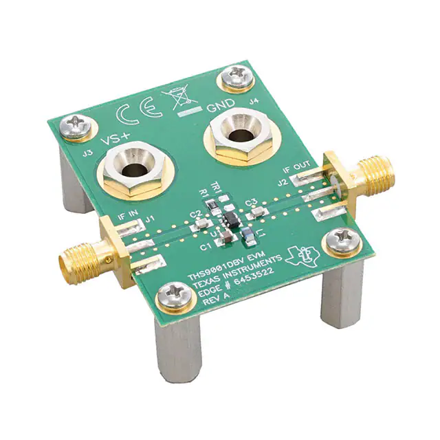
Evaluation Module
Bill Of Materials is the bill of materials, and Figure 26 and Figure 27 show the EVM layout.
Bill Of Materials
ITEM
(1)
DESCRIPTION
1
Cap, 0.1 μF, ceramic, X7R, 50 V
2
Cap, 1000 pF, ceramic, NPO, 100 V
3
Inductor, 470 nH, 5%
4
Resistor, 237 Ω, 1/8 W, 1%
5
Open
6
REF DES
QTY
PART NUMBER (1)
(AVX) 08055C104KAT2A
C1
1
C2, C3
2
(AVX) 08051A102JAT2A
L1
1
(Coilcraft) 0805CS-471XJBC
(Phycomp) 9C08052A2370FKHFT
R1
1
TR1
1
Jack, banana receptance, 0.25" dia.
J3, J4
2
(SPC) 813
7
Connector, edge, SMA PCB jack
J1, J2
2
(Johnson) 142-0701-801
8
Standoff, 4-40 Hex, 0.625" Length
4
(KEYSTONE) 1808
9
Screw, Phillips, 4-40, .250"
4
SHR-0440-016-SN
10
IC, THS90001
1
(TI) THS9001DBV
11
Board, printed-circuit
1
(TI) EDGE # 6453522 Rev.A
U1
The manufacturer's part numbers are used for test purposes only.
Figure 26. EVM Top Layout
Figure 27. EVM Bottom Layout
14
Submit Documentation Feedback
Copyright © 2003–2013, Texas Instruments Incorporated
Product Folder Links: THS9001
�THS9001
www.ti.com
SLOS426C – NOVEMBER 2003 – REVISED DECEMBER 2013
0.085
0.053
Pin 1
0.008
0.040
0.032
0.032
TOP VIEW
Figure 28. THS9000 Recommended Footprint dimensions are in inches (millimeters)
Submit Documentation Feedback
Copyright © 2003–2013, Texas Instruments Incorporated
Product Folder Links: THS9001
15
�THS9001
SLOS426C – NOVEMBER 2003 – REVISED DECEMBER 2013
www.ti.com
REVISION HISTORY
Changes from Revision B (January 2007) to Revision C
•
16
Page
Changed the data sheet title From: 50 MHz to 400 MHz CASCADEABLE AMPLIFIER To: 50 MHz to 750 MHz
CASCADEABLE AMPLIFIER ............................................................................................................................................... 1
Submit Documentation Feedback
Copyright © 2003–2013, Texas Instruments Incorporated
Product Folder Links: THS9001
�PACKAGE OPTION ADDENDUM
www.ti.com
10-Dec-2020
PACKAGING INFORMATION
Orderable Device
Status
(1)
Package Type Package Pins Package
Drawing
Qty
Eco Plan
(2)
Lead finish/
Ball material
MSL Peak Temp
Op Temp (°C)
Device Marking
(3)
(4/5)
(6)
THS9001DBVT
ACTIVE
SOT-23
DBV
6
250
RoHS & Green
NIPDAU
Level-1-260C-UNLIM
-40 to 85
NWL
(1)
The marketing status values are defined as follows:
ACTIVE: Product device recommended for new designs.
LIFEBUY: TI has announced that the device will be discontinued, and a lifetime-buy period is in effect.
NRND: Not recommended for new designs. Device is in production to support existing customers, but TI does not recommend using this part in a new design.
PREVIEW: Device has been announced but is not in production. Samples may or may not be available.
OBSOLETE: TI has discontinued the production of the device.
(2)
RoHS: TI defines "RoHS" to mean semiconductor products that are compliant with the current EU RoHS requirements for all 10 RoHS substances, including the requirement that RoHS substance
do not exceed 0.1% by weight in homogeneous materials. Where designed to be soldered at high temperatures, "RoHS" products are suitable for use in specified lead-free processes. TI may
reference these types of products as "Pb-Free".
RoHS Exempt: TI defines "RoHS Exempt" to mean products that contain lead but are compliant with EU RoHS pursuant to a specific EU RoHS exemption.
Green: TI defines "Green" to mean the content of Chlorine (Cl) and Bromine (Br) based flame retardants meet JS709B low halogen requirements of