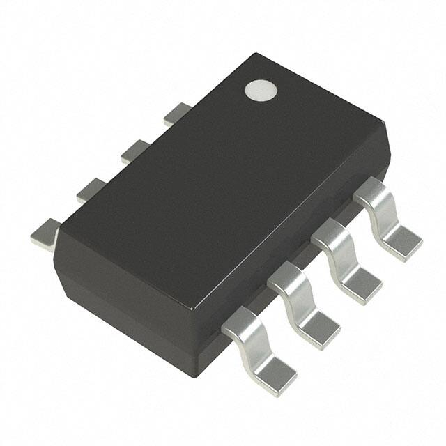
THVD8010
THVD8010
SLLSFK4 – NOVEMBER
2020
SLLSFK4 – NOVEMBER 2020
www.ti.com
THVD8010 RS-485 Transceiver with OOK Modulation for Power Line Communication
1 Features
3 Description
•
•
THVD8010 is an RS-485 transceiver with on-off
keying (OOK) modulation and demodulation built in
for power line communication. Modulating data onto
existing power lines allows power delivery and data
communication to share a common pair of wires,
resulting in a significant reduction of the system cost.
•
•
•
•
•
•
•
•
•
•
3-V – 5.5-V supply voltage
Half-duplex communication
– Up to 30 Kbps data rate (OOK)
RS-485 electrical signaling with on-off keying
(OOK) modulation
Polarity Free
Good noise immunity
Pin selectable carrier frequency: 125 kHz – 300
KHz
Spread spectrum clocking for excellent EMI
performance
TX timeout to avoid stuck bus conditions
Operational common-mode range: –7 V to 12 V
Bus I/O protection
– ± 18-V DC fault protection
– ± 16 kV HBM ESD
– ± 8 kV IEC 61000-4-2 contact discharge
– ± 15 kV IEC 61000-4-2 air gap discharge
– ± 4 kV IEC 61000-4-4 fast transient burst
Extended temperature range: -40°C to 125°C
8-Pin SOT-23 package for space constrained
applications
A pin programmable interface simplifies the system
design. The carrier frequency can be adjusted by
changing an external resistor on the F_SET pin. A
broad range of carrier frequencies gives the system
designer the flexibility to choose the external inductors
and capacitors. In addition, OOK modulation operates
with immunity to data polarity for ease of system
installations.
Device Information
PACKAGE(1)
PART NUMBER
THVD8010
(1)
SOT-23 (8)
BODY SIZE (NOM)
2.90 mm × 1.60 mm
For all available packages, see the orderable addendum at
the end of the data sheet.
2 Applications
• HVAC systems
• Building automation
• Factory automation & control
• Appliances
• Lighting
• Grid infrastructure
Spacer
AC/DC
supply
Vcc
L2
L3
L4
C1
R
MCU
L1
Load
Vcc
C3
MODE THVD8010
D
GND
R
THVD8010 MODE
C2
C4
MCU
D
GND
Simplified Schematic
An©IMPORTANT
NOTICEIncorporated
at the end of this data sheet addresses availability, warranty, changes, use in
safety-critical
applications,
Copyright
2020 Texas Instruments
Submit
Document
Feedback
intellectual property matters and other important disclaimers. PRODUCTION DATA.
Product Folder Links: THVD8010
1
�THVD8010
www.ti.com
SLLSFK4 – NOVEMBER 2020
Table of Contents
1 Features............................................................................1
2 Applications..................................................................... 1
3 Description.......................................................................1
4 Revision History.............................................................. 2
5 Pin Configuration and Functions...................................3
Pin Functions.................................................................... 3
6 Specifications.................................................................. 4
6.1 Absolute Maximum Ratings ....................................... 4
6.2 ESD Ratings .............................................................. 4
6.3 ESD Ratings - IEC Specifications .............................. 4
6.4 Recommended Operating Conditions ........................4
6.5 Thermal Information ...................................................5
6.6 Electrical Characteristics ............................................5
6.7 Power Dissipation Characteristics ............................. 8
6.8 Switching Characteristics ...........................................8
6.9 Typical Characteristics................................................ 9
7 Parameter Measurement Information.......................... 10
8 Detailed Description......................................................15
8.1 Overview................................................................... 15
8.2 Functional Block Diagrams....................................... 15
8.3 Feature Description...................................................15
8.4 Device Functional Modes..........................................17
9 Application and implementation.................................. 18
9.1 Application information..............................................18
9.2 Typical application (OOK mode)............................... 18
10 Power supply recommendations............................... 20
11 Layout........................................................................... 21
11.1 Layout guidelines.................................................... 21
11.2 Layout Example...................................................... 21
12 Device and Documentation Support..........................22
12.1 Device Support....................................................... 22
12.2 Receiving Notification of Documentation Updates..22
12.3 Support Resources................................................. 22
12.4 Trademarks............................................................. 22
12.5 Electrostatic Discharge Caution..............................22
12.6 Glossary..................................................................22
4 Revision History
NOTE: Page numbers for previous revisions may differ from page numbers in the current version.
2
DATE
REVISION
NOTES
November 2020
*
Initial release.
Submit Document Feedback
Copyright © 2020 Texas Instruments Incorporated
Product Folder Links: THVD8010
�THVD8010
www.ti.com
SLLSFK4 – NOVEMBER 2020
5 Pin Configuration and Functions
R
1
8
V
MODE
2
7
B
F_SET
3
6
A
D
4
5
GND
CC
Not to scale
Figure 5-1. DRL Package, 8-Pin SOT-23, Top View
Pin Functions
PIN
NAME
NO.
I/O
DESCRIPTION
R
1
Digital output
Receive data output
MODE
2
Digital input
Transmit/receive mode selection. Low = receive mode; High = transmit mode. Has an
internal 2-MΩ pull-down to GND
F_SET
3
Analog input
Carrier frequency selection. Use a resistor to GND to select a frequency.
D
4
Digital input
GND
5
Ground
Driver data input, 2-MΩ pull-up to VCC
A
6
Bus input/output
Bus I/O port A (complementary to B)
B
7
Bus input/output
Bus I/O port B (complementary to A)
VCC
8
Power
Device ground
3.3-V to 5-V device supply
Submit Document Feedback
Copyright © 2020 Texas Instruments Incorporated
Product Folder Links: THVD8010
3
�THVD8010
www.ti.com
SLLSFK4 – NOVEMBER 2020
6 Specifications
6.1 Absolute Maximum Ratings
see (1)
MIN
MAX
UNIT
VCC
Supply voltage
–0.5
7
V
VL
Input voltage at any logic pin (D, MODE or F_SET)
–0.3
5.7
V
VA, VB
Voltage at A or B inputs (differential or with respect to GND)
–18
18
V
IO
Receiver output current
–24
24
mA
170
°C
150
°C
TJ
Junction temperature
TSTG
Storage temperature
(1)
–65
Stresses beyond those listed under Absolute Maximum Ratings may cause permanent damage to the device. These are stress ratings
only and functional operation of the device at these or any other conditions beyond those indicated under Section 6.4 is not implied.
Exposure to absolute-maximum-rated conditions for extended periods may affect device reliability.
6.2 ESD Ratings
VALUE
V(ESD)
(1)
(2)
Electrostatic
discharge
Human body model (HBM), per ANSI/ESDA/JEDEC
JS-001(1)
Charged-device model (CDM), per JEDEC specification
JESD22-C101(2)
A and B pins to GND
±16,000
All pins
±4,000
All pins
±1,500
UNIT
V
JEDEC document JEP155 states that 500-V HBM allows safemanufacturing with a standard ESD control process.
JEDEC document JEP157 states that 250-V CDM allows safemanufacturing with a standard ESD control process.
6.3 ESD Ratings - IEC Specifications
VALUE
V(ESD)
Electrostatic discharge
IEC 61000-4-2 ESD contact discharge, A and B pins to GND
±8
IEC 61000-4-2 ESD air gap discharge, A and B pins to GND
±15
IEC 61000-4-4 electrical fast transient, A and B pins to GND
±4
UNIT
kV
6.4 Recommended Operating Conditions
MIN
MAX
UNIT
VCC
Supply voltage
3
5.5
V
VID
Input differential voltage (A and B pins)
–7
12
V
VCM
Operational common mode voltage (A and B pins)
–7
12
V
VIH
High-level input voltage (D and MODE pins)
2
VCC
V
VIL
Low-level input voltage (D and MODE pins)
0
0.8
V
Driver
–60
60
–4
4
IO
Output current
RF_SET
Carrier frequency selection resistor
32
80
kΩ
Carrier frequency selection resistor tolerance
–2
2
%
ΔR
F_SET
Receiver
Modulation mode(1)
1/tUI
Data rate
CF_SET
Recommended load capacitance on F_SET pin
TA
Operating ambient temperature
(1)
4
NOM
–40
mA
f0 / 10
bps
100
pF
125
°C
f0 is the carrier frequency (in Hz) set by the external resistor between F_SET and GND pins.
Submit Document Feedback
Copyright © 2020 Texas Instruments Incorporated
Product Folder Links: THVD8010
�THVD8010
www.ti.com
SLLSFK4 – NOVEMBER 2020
6.5 Thermal Information
THVD8010
THERMAL METRIC(1)
UNIT
DDF (SOT-23)
8 PINS
RθJA
Junction-to-ambient thermal resistance
106.6
°C/W
RθJC(top)
Junction-to-case (top) thermal resistance
38.4
°C/W
RθJB
Junction-to-board thermal resistance
29.9
°C/W
ψJT
Junction-to-top characterization parameter
1.9
°C/W
ψJB
Junction-to-top characterization parameter
29.5
°C/W
(1)
For more information about traditional and new thermalmetrics, see the Semiconductor and ICPackage Thermal Metrics application
report.
6.6 Electrical Characteristics
over operating free-air temperature range (unless otherwise noted). All typical values are at 25°C and supply voltage of VCC
= 5 V.
PARAMETER
TEST CONDITIONS
MIN
TYP
OOK mode, RL = 60 Ω, –7 V ≤
Vtest ≤ 12 V, Measured at 2nd See Figure 7-1
pulse
1.5
2
OOK mode, RL = 100 Ω, CL =
See Figure 7-1
50 pF, Measured at 2nd pulse
2
2.5
OOK mode, RL = 54 Ω, CL =
See Figure 7-1
50 pF, Measured at 2nd pulse
1.5
2
VCC / 2
MAX
UNIT
Driver
|VOD|
Driver differential output
voltage magnitude
V
VOC
Steady state common-mode OOK mode, RL = 60 Ω, CL =
output voltage
50 pF
See Figure 7-2
1
ΔVOC
Change in differential driver
common-mode output
voltage
OOK mode, RL = 60 Ω, CL =
50 pF
See Figure 7-2
-160
VOC(PP)
Peak-to-peak driver
common-mode output
voltage
OOK mode, RL = 60 Ω, CL =
50 pF, VCC = 3.3 V and VCC =
5V
See Figure 7-2
IOS
Driver short-circuit output
current
OOK mode, MODE = VCC, –7 V ≤ [VA or VB] ≤
12 V
f0
Minimum carrier frequency(1) RF_SET = 77 kΩ
See Figure 7-3
125
kHz
f0
Maximum carrier
frequency(1)
RF_SET = 31.9 kΩ
See Figure 7-3
300
kHz
DCDf0
Carrier frequency duty cycle
distortion
Measured over the full range of f0
Δf0
Carrier frequency tolerance
Measured with a ±2% tolerant RF_SET
ΔfSSC
Variation of the carrier
frequency for spread
spectrum clocking
Measured across the full carrier frequency
range
fSSC
Spread spectrum clock rate
3
160
450
–250
V
mV
mV
250
mA
–2
2
%
–25
25
%
±5
%
30
kHz
Submit Document Feedback
Copyright © 2020 Texas Instruments Incorporated
Product Folder Links: THVD8010
5
�THVD8010
www.ti.com
SLLSFK4 – NOVEMBER 2020
6.6 Electrical Characteristics (continued)
over operating free-air temperature range (unless otherwise noted). All typical values are at 25°C and supply voltage of VCC
= 5 V.
PARAMETER
TEST CONDITIONS
MIN
TYP
MAX
75
125
–97
–70
UNIT
Receiver
MODE = GND, VCC = 0 V or
5.5 V
VI = 12 V
II
Bus input current in receive
mode
VMAG_ZERO
OOK signal differential swing MODE = GND, over full
(magnitude) to detect a zero common mode range, OOK
at the R output
mode
125 kHz
1200
mV
VMAG_ZERO
OOK signal differential swing
(magnitude) to detect a zero
at the R output
200 kHz
1200
mV
VMAG_ZERO
OOK signal differential swing MODE = GND, over full
(magnitude) to detect a zero common mode range, OOK
at the R output
mode
300 kHz
1300
mV
VMAG_ONE
OOK signal differential swing MODE = GND, over full
(magnitude) to detect an one common mode range, OOK
at the R output
mode
125 kHz
400
mV
VMAG_ONE
OOK signal differential swing
(magnitude) to detect an one
at the R output
200 kHz
400
mV
VMAG_ONE
OOK signal differential swing
(magnitude) to detect an one
at the R output
300 kHz
400
mV
VMAG_HYS
Receiver differential input
voltage threshold hysteresis
125 kHz
350
mV
VMAG_HYS
Receiver differential input
voltage threshold hysteresis
200 kHz
350
mV
VMAG_HYS
Receiver differential input
voltage threshold hysteresis
MODE = GND, over full
common mode range, OOK
mode
300 kHz
350
mV
VI = –7 V
µA
Logic / Control Pins
IIN
Input current (D, MODE)
VO = 0 V or VCC
VO = 0 V or VCC
IIN
Input current (F_SET)
VO = VCC
VO = VCC
VO
Output voltage (F_SET)
VOH
Receiver high-level output
voltage
IOH = –4 mA
VOL
Receiver low-level output
voltage
IOL = 4 mA
IOZ
Receiver high-impedance
output current
VO = 0 V or VCC, MODE = 0
–5
5
µA
55
µA
IO = 0 mA
1.4
V
32 kΩ ≤ RPD ≤ 78 kΩ
785
mV
IOH = –4 mA
VCC – 0.4
VCC – 0.2
0.2
V
0.4
V
1
µA
3
5
mA
3.8
6
mA
–1
Device
ICC
ICC
6
Supply current (quiescent)
Supply current (quiescent)
OOK transmit mode
D = VCC,
MODE = VCC,
resistor
between
F_SET and
GND, no load
OOK receive mode
D = VCC,
MODE = GND,
resistor
between
F_SET and
GND, no load
Submit Document Feedback
Copyright © 2020 Texas Instruments Incorporated
Product Folder Links: THVD8010
�THVD8010
www.ti.com
SLLSFK4 – NOVEMBER 2020
6.6 Electrical Characteristics (continued)
over operating free-air temperature range (unless otherwise noted). All typical values are at 25°C and supply voltage of VCC
= 5 V.
PARAMETER
TSD
Thermal shutdown
temperature
THYS
Thermal shutdown
hysteresis
(1)
TEST CONDITIONS
MIN
TYP
MAX
UNIT
160
170
185
℃
11
15
℃
See OOK modulation section for the complete carrier frequency range
Submit Document Feedback
Copyright © 2020 Texas Instruments Incorporated
Product Folder Links: THVD8010
7
�THVD8010
www.ti.com
SLLSFK4 – NOVEMBER 2020
6.7 Power Dissipation Characteristics
over operating free-air temperature range (unless otherwise noted). All typical values are at 25°C and supply voltage of VCC
= 5 V.
PARAMETER
PD
Chip power dissipation in OOK mode
OOK
TEST CONDITIONS
MODE = VCC, RL
= 60 Ω, no CL,
see Figure 2
TYP
MAX
UNIT
f0 = 125 kHz, 12.5
kHz (25 kbps) clock
pattern as data
MIN
60
85
mW
f0 = 300 kHz, 30 kHz
(60 Kbps) clock
pattern as data
90
130
mW
6.8 Switching Characteristics
over operating free-air temperature range (unless otherwise noted). All typical values are at 25°C and supply voltage of VCC
= 5 V.
PARAMETER
TEST CONDITIONS
MIN
TYP
MAX
8
30
UNIT
Driver
tr, tf
Driver differential output rise and fall
times
tPHL, tPLH
Driver propagation delay
1
3.5
Clocks
tSK(P)
Driver pulse skew, |tPHL – tPLH|
1
2.5
Clocks
tr, tf
Receiver output rise and fall times
2
8
tPHL, tPLH
Receiver propagation delay time
tSK(P)
Receiver pulse skew, |tPHL – tPLH|
RL = 60 Ω, CL = 50 pF, See Figure 7-4
ns
Receiver
CL = 15 pF, See Figure 7-5
4.5
6
0.4
3
ns
Clocks
Device
8
tTX-RX_OOK
Transmit to receive mode change
delay, OOK mode
Max of tTX-RX_OOK_ZERO and tTX-RX_OOK_ONE.
See Figure 7-6 and Figure 7-7
tRX-TX_OOK
Receive to transmit mode change
delay, OOK mode
See Figure 7-8
tTX_TIMEOUT
Transmit timeout delay
60
Submit Document Feedback
110
14
clocks
3
clocks
s
Copyright © 2020 Texas Instruments Incorporated
Product Folder Links: THVD8010
�THVD8010
www.ti.com
SLLSFK4 – NOVEMBER 2020
6.9 Typical Characteristics
38
300
-40C (3.3V)
25C (3.3V)
125C (3.3V)
36
-40C (5.5V)
25C (5.5V)
125C (5.5V)
260
OOK Frequency (kHz)
34
32
ICC (mA)
-40C (3.3V)
25C (3.3V)
125C (3.3V)
-40C (5.5V)
25C (5.5V)
125C (5.5V)
280
30
28
26
240
220
200
180
160
24
140
22
120
20
100
100
30
125
RL = 60Ω
150
175
200
225
OOK Frequency (kHz)
Data rate = ƒ0/10
250
275
300
ICCv
TX Enabled
40
50
60
RF_SET (k:)
70
80
90
rfse
Figure 6-2. RF_SET vs OOK Frequency
Figure 6-1. ICC vs OOK Frequency
Submit Document Feedback
Copyright © 2020 Texas Instruments Incorporated
Product Folder Links: THVD8010
9
�THVD8010
www.ti.com
SLLSFK4 – NOVEMBER 2020
7 Parameter Measurement Information
Note
The number of pulses shown is reduced for simplicity of waveform. Please see the "OOK Modulation
with F_SET pin" section for more information.
375
A
VOD
GND
D
RL
+
B
±
Vtest
375
OOK mode
A
VOD
B
Figure 7-1. Measurement of Driver Differential Output Voltage With Common-Mode Load
RL / 2
A
D
VOD
VCC or
GND
RL / 2
CL
VOC
B
OOK mode
D
A
B
VOD = VA - VB
ûVOC
VOC
VOC(PP)
Figure 7-2. Measurement of Driver Differential and Common-Mode Outputs
10
Submit Document Feedback
Copyright © 2020 Texas Instruments Incorporated
Product Folder Links: THVD8010
�THVD8010
www.ti.com
SLLSFK4 – NOVEMBER 2020
D
tUI
A
B
1 / f0
Figure 7-3. Measurement of Carrier Frequency
A
Clock D
pattern
RL
CL
B
OOK mode
D
tPLH
tPHL
50%
A
B
VA - VB
90%
60%
VOD
10%
tr
tf
Figure 7-4. Measurement of Driver Switching Characteristics
Submit Document Feedback
Copyright © 2020 Texas Instruments Incorporated
Product Folder Links: THVD8010
11
�THVD8010
www.ti.com
SLLSFK4 – NOVEMBER 2020
THVD8010 as
the generator
DUT
A
Clock D
pattern
60 �
R
50 pF
CL
B
OOK mode
D
A
B
V A - VB
90%
60%
R
90%
50%
10%
VOD
tPLH
tPHL
tf
tr
Figure 7-5. Measurement of Receiver Characteristics
12
Submit Document Feedback
Copyright © 2020 Texas Instruments Incorporated
Product Folder Links: THVD8010
�THVD8010
www.ti.com
SLLSFK4 – NOVEMBER 2020
VCC
DUT
A
1 kΩ
R
B
15 pF
MODE
OOK mode
MODE
F0 = 300 kHz
50%
A
750 mV
Hi-Z
-750 mV
B
R
50%
100 ns
tTX-RX_OOK_ZERO
Figure 7-6. Transmit to Receive Mode Change with Low Output
DUT
A
R
B
15 pF
1k
MODE
OOK mode
MODE
50%
A
Hi-Z
0V
B
R
50%
100 ns
tTX-RX_OOK_ONE
Figure 7-7. Transmit to Receive Mode Change with High Output
Submit Document Feedback
Copyright © 2020 Texas Instruments Incorporated
Product Folder Links: THVD8010
13
�THVD8010
www.ti.com
SLLSFK4 – NOVEMBER 2020
A
D
60
50 pF
B
MODE
OOK mode
MODE
50%
A
B
90%
VOD
A-B
tRX-TX_OOK
Figure 7-8. Receive to Transmit Mode Change
14
Submit Document Feedback
Copyright © 2020 Texas Instruments Incorporated
Product Folder Links: THVD8010
�THVD8010
www.ti.com
SLLSFK4 – NOVEMBER 2020
8 Detailed Description
8.1 Overview
THVD8010 enables power line communication using RS-485 physical layer signaling. An integrated OOK
modulator enables RS-485 data to be directly coupled onto existing power cables via series capacitors without
any updates to the MCU or the controller. The THVD8010 receiver extracts the data from the power cables
through series capacitors by using a precise bandpass filter and a demodulator.
8.2 Functional Block Diagrams
VCC
A
D
B
F_SET
MODE
Logic &
Control
R
Demodulation
GND
8.3 Feature Description
8.3.1 OOK Modulation with F_SET pin
Data at the D input is modulated with the carrier frequency (f 0) which is set via the F_SET pin. Figure 8-1
illustrates the modulation scheme. A high level at the D input is driven to the mid-level with zero differential
voltage (VOD). A low level at the D input is modulated at the carrier frequency. It is recommended to use a carrier
frequency that is 10x higher than the data rate. Higher data rates are possible at the expense of increased pulse
width distortion with the use of lower ratios.
Data input: D
Bus at driver
pins: A / B
Figure 8-1. OOK Modulation Scheme
Submit Document Feedback
Copyright © 2020 Texas Instruments Incorporated
Product Folder Links: THVD8010
15
�THVD8010
www.ti.com
SLLSFK4 – NOVEMBER 2020
f 0 is programmable by changing the external resistor (R F_SET) value connected to ground. Table 8-1 shows the
carrier frequency for the each recommended resistor value.
Table 8-1. OOK f0 versus RF_SET
RF_SET (kΩ)
OOK f0 (kHz)
77
125
50
187.5
31.9
300
The oscillator used to generate the carrier frequency features spread spectrum clocking to reduce emissions.
8.3.2 OOK Demodulation
The OOK signal received at the A and B inputs go through a bandpass filter and a peak detector to regenerate
the original data stream. Figure 8-2 shows the OOK input and the R output waveforms. The bandpass filter
characteristics will adapt to optimal settings automatically based on the carrier frequency, set via RF_SET.
Bus at receiver
pins: A / B
Data output: R
Figure 8-2. OOK Demodulation
8.3.3 Transmitter Timeout
The driver path incorporates a timeout feature to prevent a faulty node from occupying the bus indefinitely in a
multi-drop application.
The driver stops transmitting and the outputs go high impedance if the D input doesn't detect an edge (either
rising or falling) for longer than t TX_TIMEOUT. One of the following events brings the device back to normal
operation.
• Any edge at D input
• Toggle MODE pin
The transmit path resumes operation within tMODE.
8.3.4 Polarity Free Operation
THVD8010 is immune to A and B polarity at the receiver input in OOK mode. The receiver data comparator only
checks for the receive input signal magnitude, ignoring the polarity, to determine its logic level. Note that
reversing the polarity does result in degraded pulse width distortion.
8.3.5 Glitch Free Mode Change
The device incorporates a delay of up to t MODE when changing the state of the MODE pin. This feature ensures
that there are no glitches at the A, B and R outputs when transitioning between transmit and receive modes.
8.3.6 Integrated IEC ESD and EFT Protection
Internal ESD protection circuits protect the transceiver against electrostatic discharges (ESD) according to IEC
61000-4-2 of up to ±8 kV contact and against electrical fast transients (EFT) according to IEC 61000-4-4 of up to
±4 kV. This integrated protection eliminates the need of external components reducing the system BOM.
16
Submit Document Feedback
Copyright © 2020 Texas Instruments Incorporated
Product Folder Links: THVD8010
�THVD8010
www.ti.com
SLLSFK4 – NOVEMBER 2020
8.4 Device Functional Modes
Table 8-2. Functional Modes
F_SET Configuration
Device Functional Mode
RF_SET between F_SET and GND
OOK mode, f0 set by the RF_SET value
F_SET at high impedance
F_SET at VCC
Invalid, not recommended for normal operation
F_SET short to GND
8.4.1 OOK Mode
Data at the D input is modulated with the carrier frequency set by the R F_SET value when the device is
transmitting (MODE = V CC). See Section 8.3.1 section for more details. In receiving (MODE = GND), the device
expects an OOK modulated signal at the A and B inputs. The data is demodulated and sent out via R pin. See
Section 8.3.2 section for more details.
Table 8-3. Driver function table for OOK mode
INPUTS
OUTPUTS
FUNCTION
F_SET
MODE
D
A
B
RF_SET (See Table 8-1)
H
H or Z
Bias to VCM
Bias to VCM
Driver is actively biased to
VCM on the bus
H
L
Oscillating
Oscillating
Bus actively driven at
carrier frequency
L or Z
X
Z
Z
Driver disabled, device in
receive mode
Table 8-4. Receiver function table for OOK mode
INPUTS
OUTPUT
FUNCTION
F_SET
MODE
Input
R
RF_SET (See Table 8-1)
L or Z
Oscillating at F_SET and VID > V
L
Receive valid bus low
Oscillating at F_SET and V
< VID < VMAG_ZERO
?
Receive invalid bus, output
indeterminate
Oscillating at F_SET and VID < V
H
Receive valid bus high
Receive valid bus high
MAG_ZERO
L or Z
MAG_ONE
L or Z
MAG_ONE
L or Z
Z / not oscillating
H
L or Z
OPEN, SHORT, IDLE (VID = 0 V)
H
Failsafe high output
H
X
Z
Receiver disabled, device in
transmit mode
8.4.2 Thermal shutdown (TSD)
The THVD8010 has a protection feature called thermal shutdown. When the junction temperature reaches T SD,
the device enters thermal shutdown protection mode. This mode disables the driver and receiver outputs, which
will halt all communication through the device. Normal operation resume once the junction temperature drops out
of thermal shutdown, which is typically TSD - THYS.
Submit Document Feedback
Copyright © 2020 Texas Instruments Incorporated
Product Folder Links: THVD8010
17
�THVD8010
www.ti.com
SLLSFK4 – NOVEMBER 2020
9 Application and implementation
Note
Information in the following applications sections is not part of the TI component specification, and TI
does not warrant its accuracy or completeness. TI’s customers are responsible for determining
suitability of components for their purposes. Customers should validate and test their design
implementation to confirm system functionality.
9.1 Application information
The THVD8010 is able to transmit data over an AC coupled power line pair using On-Off Keying (OOK).
9.2 Typical application (OOK mode)
In order to combine data and power over a single pair of wires, capacitors and inductors are used in a bias-tee
configuration. High-frequency differential data is AC-coupled onto the bus lines via series capacitances while
power is DC-coupled via series inductances. The values of these components will depend on the carrier
frequency, number of nodes on the bus, and the power delivery requirements (i.e., voltage and total current
sourced or consumed by a given node).
In Figure 9-1, there is an optional rectifier network pictured on the bus lines. This network of diodes can ensure
that the node is receives power correctly from the bus wires, even if the lines get swapped.
A termination resistance, RT, is not required for device functionality but can be useful in improving signal integrity
in some applications by reducing reflections that can occur at cable ends.
Sing le Nod e
VIN
VOUT
LDO
GND
Sup ply
VCC
R
Ln
R
A
MODE
D
B
Ln
RT
Single Node
C
D
L1
C
L1
F_SET
RFSET
GND
GND
Figure 9-1. Typical power line network with 2 nodes
9.2.1 Design requirements
The main requirements are the values of the bus capacitors and the power inductors. Both of these values are
dependant upon the carrier frequency selected.
9.2.1.1 Carrier frequency
This device uses on-off-keying to transmit binary data on the bus. Please read Section 8.3.1 for detailed
information. The modulation and demodulation of the data can result in pulse width distortion due to
asymmetries in low-to-high and high-to-low transition times. These asymmetries are due to factors like
18
Submit Document Feedback
Copyright © 2020 Texas Instruments Incorporated
Product Folder Links: THVD8010
�THVD8010
www.ti.com
SLLSFK4 – NOVEMBER 2020
synchronization of the data to the internal carrier oscillator in the transmit path and the response time of the
band-pass filter in the receive path. The impact of these factors can be minimized by choosing a carrier
frequency much higher than the data rate required. A frequency ratio of at least 10:1 is recommended.
9.2.2 Detailed design procedure
9.2.2.1 Inductor value selection
It is important to note that the inductor selected must also take power consumption into consideration. The
inductor should be sized to handle the maximum anticipated current in addition to the inductance value.
The parallel aggregate impedance should be selected so that the total equivalent impedance at the carrier
frequency is Z ≥ 375 Ω. This assumes RS-485 loading with 60 Ω termination. If no termination is used in the
application, then the total equivalent impedance at the carrier frequency could be reduced to Z ≥ 60 Ω. These
examples assume that termination is used. Equation 1 shows the parallel aggregate impedance equation for
inductors L 1 to L n. Since the inductance value for each node should be the same, it's simple to determine that
each node's impedance should be n times the total equivalent impedance. For example, if there are 4 nodes
connected to the bus and the equivalent impedance is 375 Ω, then each node impedance should be 1,500 Ω.
< =