Product
Folder
Order
Now
Support &
Community
Tools &
Software
Technical
Documents
TIC12400
SCPS269 – SEPTEMBER 2017
TIC12400 24-Input Multiple Switch Detection Interface (MSDI) Device
With Integrated ADC and Adjustable Wetting Current
1 Features
3 Description
•
The TIC12400 is an advanced Multiple Switch
Detection Interface (MSDI) device designed to detect
external switch statuses. The TIC12400 supports 24
direct inputs, with 10 inputs configurable to monitor
digital I/O switches. 6 wetting current settings can be
programmed for each input to support different
application scenarios. The TIC12400 features an
integrated 10-bit ADC to monitor multi-position analog
switches and a comparator to monitor digital switches
independently of the MCU. The device supports
wake-up operation on all switch inputs to eliminate
the need to keep the MCU active continuously, thus
reducing power consumption of the system. The
TIC12400 supports 2 modes of operations:
continuous and polling mode. In continuous mode,
wetting current is supplied continuously. In polling
mode, wetting current is turned on periodically to
sample the input status based on a programmable
timer, thus the system power consumption is
significantly reduced. The TIC12400 also offers
various fault detection and diagnostic features for
improved system robustness.
1
•
•
•
•
•
•
•
•
•
•
•
Operates with Supply Voltage (VS) from 6.5 V to
35 V with Over-voltage and Under-voltage
Warning
Monitors up 24 Direct Switch Inputs with 10 Inputs
Configurable to Monitor Switches Connected to
Either Ground or Supply
Switch Input Withstands 40 V and Reverse Supply
Condition Down to -24 V
6 Configurable Wetting Current Settings:
(0 mA, 1 mA, 2 mA, 5 mA, 10 mA, and 15 mA)
Integrated 10-bit ADC for Multi-Position Analog
Switch Monitoring
Integrated Comparator with 4 Programmable
Threshold for Input Monitoring
Ultra-low Operating Current in Polling Mode:
68 μA Typical (tPOLL = 64 ms, tPOLL_ACT = 128 μs,
All 24 Inputs Active, Comparator Mode, All
Switches Open)
Interfaces Directly to MCU Using 3.3 V/5 V Serial
Peripheral Interface (SPI) Protocol
Interrupt Generation to Support Wake-Up
Operation on All Inputs
Integrated Supply and Temperature Sensing
±8 kV Contact Discharge ESD Protection on Input
Pins per IEC 61000-4-2 With Appropriate External
Components
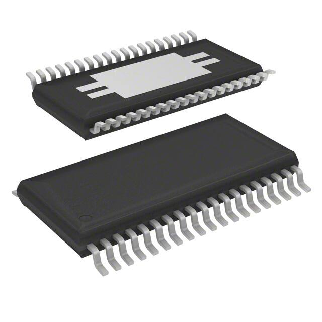
38-Pin TSSOP Package
Device Information(1)
PART NUMBER
PACKAGE
TIC12400
TSSOP (38)
BODY SIZE (NOM)
9.70 mm x 4.40 mm
(1) For all available packages, see the orderable addendum at
the end of the data sheet.
Simplified Schematic
VSUPPLY
Voltage
Regulator
2 Applications
•
•
•
Signal Measurement
PLC, DCS and PAC
Instrumentation
VSUPPLY
VS
VS
IN0
400 O
VDD
VDD
IN9
/INT
/INT
/CS
/CS
IN10
SCLK
SCLK
SI
MOSI
SO
MISO
VSUPPLY
400 O
Sensor
Sensor
IN23
TIC12400
Microcontroller
Copyright © 2017, Texas Instruments Incorporated
1
An IMPORTANT NOTICE at the end of this data sheet addresses availability, warranty, changes, use in safety-critical applications,
intellectual property matters and other important disclaimers. PRODUCTION DATA.
�TIC12400
SCPS269 – SEPTEMBER 2017
www.ti.com
Table of Contents
1
2
3
4
5
6
Features ..................................................................
Applications ...........................................................
Description .............................................................
Revision History.....................................................
Pin Configuration and Functions .........................
Specifications.........................................................
6.1
6.2
6.3
6.4
6.5
6.6
6.7
7
8
1
1
1
2
3
5
Absolute Maximum Ratings ...................................... 5
ESD Ratings ............................................................ 5
Recommended Operating Conditions....................... 5
Thermal Information .................................................. 6
Electrical Characteristics........................................... 6
Timing Requirements ............................................... 9
Typical Characteristics ............................................ 10
8.5 Programming .......................................................... 45
8.6 Register Maps ......................................................... 49
8.7 Programming Guidelines....................................... 121
9
9.1 Application Information.......................................... 124
9.2 Digital IO Switches and Analog Voltage
Monitoring .............................................................. 124
10 Power Supply Recommendations ................... 127
11 Layout................................................................. 128
11.1 Layout Guidelines ............................................... 128
11.2 Layout Example .................................................. 129
12 Device and Documentation Support ............... 130
12.1 Receiving Notification of Documentation
Updates..................................................................
12.2 Community Resources........................................
12.3 Trademarks .........................................................
12.4 Electrostatic Discharge Caution ..........................
12.5 Glossary ..............................................................
Parameter Measurement Information ................ 12
Detailed Description ............................................ 13
8.1
8.2
8.3
8.4
Overview .................................................................
Functional Block Diagram .......................................
Feature Description.................................................
Device Functional Modes........................................
13
14
15
28
Application and Implementation ...................... 124
130
130
130
130
130
13 Mechanical, Packaging, and Orderable
Information ......................................................... 130
4 Revision History
DATE
REVISION
September 2017
*
NOTES
Initial release.
spacer
2
Submit Documentation Feedback
Copyright © 2017, Texas Instruments Incorporated
Product Folder Links: TIC12400
�TIC12400
www.ti.com
SCPS269 – SEPTEMBER 2017
5 Pin Configuration and Functions
DCP Package
38-Pin TSSOP
Top View
IN13
1
38
VS
IN14
2
37
VS
IN15
3
36
IN12
IN16
4
35
IN11
IN17
5
34
IN10
IN18
6
33
IN9
IN19
7
32
IN8
IN20
8
31
IN7
AGND
9
30
IN6
29
IN5
Exposed
Pad
IN21
10
IN22
11
28
DGND
IN23
12
27
IN4
IN0
13
26
IN3
IN1
14
25
IN2
/CS
15
24
/INT
SCLK
16
23
CAP_D
SI
17
22
CAP_PRE
SO
18
21
RESET
VDD
19
20
CAP_A
Not to Scale
Pin Functions
PIN
NO.
NAME
TYPE (1)
DESCRIPTION
1
IN13
I/O
Ground switch monitoring input with current source
2
IN14
I/O
Ground switch monitoring input with current source
3
IN15
I/O
Ground switch monitoring input with current source
4
IN16
I/O
Ground switch monitoring input with current source
5
IN17
I/O
Ground switch monitoring input with current source
6
IN18
I/O
Ground switch monitoring input with current source
7
IN19
I/O
Ground switch monitoring input with current source
8
IN20
I/O
Ground switch monitoring input with current source
9
AGND
P
10
IN21
I/O
Ground switch monitoring input with current source
11
IN22
I/O
Ground switch monitoring input with current source
12
IN23
I/O
Ground switch monitoring input with current source
13
IN0
I/O
Ground/VSUPPLY switch monitoring input with configurable current sink or source.
14
IN1
I/O
Ground/VSUPPLY switch monitoring input with configurable current sink or source.
(1)
Ground for analog circuitry
I = input, O = output, I/O = input and output, P = power.
Submit Documentation Feedback
Copyright © 2017, Texas Instruments Incorporated
Product Folder Links: TIC12400
3
�TIC12400
SCPS269 – SEPTEMBER 2017
www.ti.com
Pin Functions (continued)
PIN
NO.
NAME
TYPE (1)
DESCRIPTION
15
CS
I
Active-low input. Chip select from the master for the SPI Interface.
16
SCLK
I
Serial clock output from the master for the SPI Interface
17
SI
I
Serial data input for the SPI Interface.
18
SO
O
Serial data output for the SPI Interface
19
VDD
P
3.3 V to 5.0 V logic supply for the SPI communication. The SPI I/Os are not fail-safe
protected: VDD needs to be present during any SPI traffic to avoid excessive leakage
currents and corrupted SPI I/O logic levels.
20
CAP_A
I/O
21
RESET
I
22
CAP_Pre
I/O
External capacitor connection for the pre-regulator. Use capacitance value of 1μF.
23
CAP_D
I/O
External capacitor connection for the digital LDO. Use capacitance value of 100nF.
24
INT
O
Open drain output. Pulled low (internally) upon change of state on the input or occurrence of
a special event.
25
IN2
I/O
Ground/VSUPPLY switch monitoring input with configurable current sink or source.
26
IN3
I/O
Ground/VSUPPLY switch monitoring input with configurable current sink or source.
27
IN4
I/O
Ground/VSUPPLY switch monitoring input with configurable current sink or source.
28
DGND
P
29
IN5
I/O
Ground/VSUPPLY switch monitoring input with configurable current sink or source.
30
IN6
I/O
Ground/VSUPPLY switch monitoring input with configurable current sink or source.
31
IN7
I/O
Ground/VSUPPLY switch monitoring input with configurable current sink or source.
32
IN8
I/O
Ground/VSUPPLY switch monitoring input with configurable current sink or source.
33
IN9
I/O
Ground/VSUPPLY switch monitoring input with configurable current sink or source.
34
IN10
I/O
Ground switch monitoring input with current source
35
IN11
I/O
Ground switch monitoring input with current source
36
IN12
I/O
Ground switch monitoring input with current source
37
VS
P
Power supply input pin.
38
VS
P
Power supply input pin.
---
EP
P
Exposed Pad. The exposed pad is not electrically connected to AGND or DGND. Connect
EP to the board ground to achieve rated thermal and ESD performance.
4
External capacitor connection for the analog LDO. Use capacitance value of 100nF.
Keep RESET low for normal operation and drive RESET high and release it to perform a
hardware reset of the device. The RESET pin is connected to ground via a 1MΩ pull-down
resistor. If not used, the RESET pin shall be grounded to avoid any accidental device reset
due to coupled noise onto this pin.
Ground for digital circuitry
Submit Documentation Feedback
Copyright © 2017, Texas Instruments Incorporated
Product Folder Links: TIC12400
�TIC12400
www.ti.com
SCPS269 – SEPTEMBER 2017
6 Specifications
6.1 Absolute Maximum Ratings
over operating free-air temperature range (unless otherwise noted) (1)
MIN
MAX
UNIT
VS, INT
-0.3
40
V
VDD, SCLK, SI, SO, CS, RESET
-0.3
6
V
IN0- IN23
-24
40
V
CAP_Pre
-0.3
5.5
V
CAP_A
-0.3
5.5
V
CAP_D
-0.3
2
V
Operating junction temperature, TJ, VS = 18 V
-40
125
°C
Operating junction temperature, TJ, VS = 24 V
-40
95
°C
Storage temperature, Tstg
-55
155
°C
Input voltage
(1)
Stresses beyond those listed under Absolute Maximum Ratings may cause permanent damage to the device. These are stress ratings
only, which do not imply functional operation of the device at these or any other conditions beyond those indicated under Recommended
Operating Conditions. Exposure to absolute-maximum-rated conditions for extended periods may affect device reliability.
6.2 ESD Ratings
VALUE
Human-body model (HBM), per ANSI/ESDA/JEDEC JS-001 (1)
V(ESD)
Electrostatic
discharge
Charged-device model (CDM), per JEDEC specification JESDC101 (1)
Contact discharge per IEC61000-4-2 contact discharge
(1)
(2)
(3)
(4)
(3) (4)
All pins
±2000
Pins IN0-IN23 (2)
±4000
All pins
±500
Corner pins (pin 1, 19, 20
and 38)
±750
Pins IN0-IN23v
±8000
UNIT
V
JEDEC document JEP155 that 500-V HBM allows safe manufacturing with a standard ESD control process. Manufacturing with less
than 500-V HBM is possible if necessary if precautions are taken.
±4kV rating on pins IN0-IN23 are stressed with respect to GND (with AGND, DGND, and EP tied together).
External components: capacitor = 15 nF; resistor = 33 Ω
ESD generator parameters: storage capacitance = 150 pF or 330pF; discharge resistance = 330 Ω or 2000 Ω
6.3 Recommended Operating Conditions
over operating free-air temperature range and VS = 12 V (unless otherwise noted)
MIN
NOM
MAX
UNIT
Power supply voltage, TA = -40 °C to 105 °C
6.5
18
V
Power supply voltage, TA = -40 °C to 85 °C
6.5
24
V
VDD
Logic supply voltage
3.0
5.5
V
V/INT
INT pin voltage
0
35
V
VINX
IN0 to IN23 input voltage
0
35
V
VRESET
RESET pin voltage
0
5.5
V
VSPI_IO
SPI input/output logic level
0
VDD
V
(1)
VS
fSPI
SPI communication frequency
4M
Hz
TA
Operating free-air temperature, VS = 18 V
-40
102
°C
TA
Operating free-air temperature, VS = 24 V
-40
85
°C
(1)
20
Lowest frequency characterized.
Submit Documentation Feedback
Copyright © 2017, Texas Instruments Incorporated
Product Folder Links: TIC12400
5
�TIC12400
SCPS269 – SEPTEMBER 2017
www.ti.com
6.4 Thermal Information
TIC10024-Q1
THERMAL METRIC (1)
DCP (TSSOP)
UNIT
38 PINS
RθJA
Junction-to-ambient thermal resistance
33.6
°C/W
RθJC(top)
Junction-to-case (top) thermal resistance
18.4
°C/W
RθJB
Junction-to-board thermal resistance
15.2
°C/W
ψJT
Junction-to-top characterization parameter
0.5
°C/W
ψJB
Junction-to-board characterization parameter
15.0
°C/W
RθJC(bot)
Junction-to-case (bottom) thermal resistance
1.2
°C/W
(1)
For more information about traditional and new thermal metrics, see the Semiconductor and IC Package Thermal Metrics application
report.
6.5 Electrical Characteristics
over operating free-air temperature range, VS = 6.5 V to 35 V, and VDD = 3 V to 5.5 V (unless otherwise noted)
PARAMETER
TEST CONDITIONS
MIN
TYP
MAX
UNIT
Continuous mode, IWETT= 10 mA, all switches open, no active
comparator operation, no unserviced interrupt
5.6
7
mA
TA= 25°
68
100
µA
68
110
µA
68
170
µA
Reset mode, VRESET= VDD. VS= 12 V, all switches open, TA=25°C
12
17
µA
TRIGGER bit in CONFIG register = logic 0, TA= 25°C, no
unserviced interrupt
50
75
µA
TRIGGER bit in CONFIG register = logic 0, TA= -40°C to 85°C, no
unserviced interrupt
50
95
µA
TRIGGER bit in CONFIG register = logic 0, TA= -40°C to 125°C,
no unserviced interrupt
50
145
µA
SCLK = SI = 0 V, CS = INT = VDD, no SPI communication
1.5
10
µA
POWER SUPPLY
Continuous mode VS
power supply current
IS_CONT
IS_POLL_COMP_25
IS_POLL_COMP_85
IS_POLL_COMP
Polling mode VS
power supply
average current
Reset mode VS
power supply current
IS_RESET
IS_IDLE_25
IS_IDLE_85
VS power supply
average current in
idle state
IS_IDLE
Logic supply current
from VDD
IDD
VPOR_R
Power on reset
(POR) voltage for VS
VPOR_F
VOV_R
Over-voltage (OV)
condition for VS
VOV_HYST
Over-voltage (OV)
condition hysteresis
for VS
VUV_R
Under-voltage (UV)
condition for VS
VUV_F
VUV_HYST
Threshold for rising VS from device OFF condition resulting in INT
pin assertion and a flagged POR bit in the INT_STAT register
3.85
4.5
V
Threshold for falling VS from device normal operation to reset
mode and loss of SPI communication
1.95
2.8
V
35
40
V
1
3.5
V
Threshold for rising VS from under-voltage condition resulting in
INT pin assertion and a flagged UV bit in the INT_STAT register
3.85
4.5
V
Threshold for falling VS from under-votlage condition resulting in
INT pin assertion and a flagged UV bit in the INT_STAT register
3.7
4.4
V
75
275
mV
2.5
2.9
V
50
150
mV
Threshold for rising VS from device normal operation resulting in
INT pin assertion and a flagged OV bit in the INT_STAT register
Threshold for falling VDD resulting in loss of SPI communication
VDD_HYST
6
TA= -40° to 105°C
Polling mode, tPOLL= 64 ms, tPOLL_ACT= 128
µs, all switches open, IWETT= 10 mA, no
unserviced interrupt
Under-voltage (UV)
condition hysteresis
for VS (1)
VDD_F
(1)
TA= -40° to 85°C
Valid VDD voltage
hysteresis
Specified by design.
Submit Documentation Feedback
Copyright © 2017, Texas Instruments Incorporated
Product Folder Links: TIC12400
�TIC12400
www.ti.com
SCPS269 – SEPTEMBER 2017
Electrical Characteristics (continued)
over operating free-air temperature range, VS = 6.5 V to 35 V, and VDD = 3 V to 5.5 V (unless otherwise noted)
PARAMETER
TEST CONDITIONS
MIN
TYP
MAX
UNIT
WETTING CURRENT ACCURACY (DIGITAL SWITCHES, MAXIMUM RESISTANCE VALUE WITH SWITCH CLOSED ≤ 100Ω , MINIMUM RESISTANCE
VALUE WITH SWITCH OPEN ≥ 5000 Ω)
IWETT (CSO)
Wetting current
accuracy for CSO
(switch closed)
1 mA setting
0.84
1
1.14
2 mA setting
1.71
2
2.32
5 mA setting
4.3
5
5.6
10 mA setting
8.4
10
11.4
15 mA setting
12.5
15
17
0.75
1.1
2.05
2 mA setting
1.6
2.2
3.3
5 mA setting
4.3
5.6
7.1
10 mA setting
9.2
11.5
13.4
15 mA setting
13.7
16.5
19.2
1 mA setting
IWETT (CSI)
VCSI_DROP_OPEN
VCSI_DROP_CLOSED
Wetting current
accuracy for CSI
(switch closed)
10 mA setting,
RSW= 5kΩ
Voltage drop from INx
pin to AGND across
15 mA setting,
CSI (switch open)
RSW= 5kΩ
Voltage drop from
INx pin to ground
across CSI (switch
closed)
6.5 V ≤ VS ≤ 35 V
mA
1.7
6.5 V ≤ VS ≤ 35V
V
1.7
2mA setting, IIN=
1mA
1.2
V
5mA setting, IIN=
1mA or 2mA
1.3
V
1.5
V
2.1
V
10mA setting, IIN=
1mA, 2mA, or
5mA
6.5 V ≤ VS ≤ 35V
15mA setting, IIN=
1mA, 2mA, 5mA,
or 10mA
LEAKAGE CURRENTS
IIN_LEAK_OFF
IIN_LEAK_OFF_25
Leakage current at
input INx when
channel is disabled
0 V ≤ VINx ≤ VS , channel disabled (EN_INx register bit= logic 0)
-4
5.3
0 V ≤ VINx ≤ VS , channel disabled (EN_INx register bit= logic 0),
TA = 25°C
-0.5
0.5
-110
110
IIN_LEAK_0mA
Leakage current at
input INx when
wetting current
setting is 0mA
0 V ≤ VINx ≤ 6 V, 6.5 V ≤ VS ≤ 35 V , IWETT setting = 0 mA
IIN_LEAK_LOSS_OF_GND
Leakage current at
input INx under loss
of GND condition
VS = 24 V, 0 V ≤ VINx ≤ 24 V, all grounds (AGND, DGND, and EP)
= 24 V, VDD shorted to the grounds (1)
IIN_LEAK_LOSS_OF_VS
Leakage current at
input INx under loss
of VS condition
0 V ≤ VINx ≤ 24 V, VS shorted to the grounds = 0 V, VDD = 0 V
µA
µA
-5
µA
µA
5
µA
LOGIC LEVELS
I/INT = 2 mA
0.35
I/INT = 4 mA
0.6
V/INT_L
INT output low
voltage
VSO_L
SO output low
voltage
ISO = 2 mA
VSO_H
SO output high
voltage
ISO = -2 mA
VIN_L
SI, SCLK, and CS
input low voltage
VIN_H
SI, SCLK, and CS
input high voltage
VRESET_L
RESET input low
voltage
VRESET_H
RESET input high
voltage
RRESET_25
RRESET
RESET pin internal
pull-down resistor
0.2VDD
0.8VDD
0.7VDD
1.6
0.85
0.2
Product Folder Links: TIC12400
V
V
1.25
1.7
2.1
Submit Documentation Feedback
Copyright © 2017, Texas Instruments Incorporated
V
V
0.8
VRESET = 0 to 5.5V, TA = –40° to 105°C
V
V
0.3VDD
VRESET = 0 to 5.5V, TA = 25°C
V
MΩ
7
�TIC12400
SCPS269 – SEPTEMBER 2017
www.ti.com
Electrical Characteristics (continued)
over operating free-air temperature range, VS = 6.5 V to 35 V, and VDD = 3 V to 5.5 V (unless otherwise noted)
PARAMETER
TEST CONDITIONS
MIN
TYP
MAX
UNIT
1.85
2.25
V
2.4
2.9
V
COMPARATOR PARAMETERS
VTH_
COMP_2V
Comparator threshold
THRES_COMP = 2 V
for 2 V
VTH_
COMP_2p7V
Comparator threshold
THRES_COMP = 2.7 V
for 2.7 V
VTH_
COMP_3V
Comparator threshold
THRES_COMP = 3 V
for 3 V
2.85
3.3
V
VTH_
COMP_4V
Comparator threshold
THRES_COMP = 4 V
for 4 V
3.7
4.35
V
THRES_COMP = 2 V
30
130
THRES_COMP = 2.7 V
35
130
THRES_COMP = 3 V
35
105
THRES_COMP = 4 V
43
95
RIN,
8
COMP
Comparator
equivalent input
resistance
Submit Documentation Feedback
kΩ
Copyright © 2017, Texas Instruments Incorporated
Product Folder Links: TIC12400
�TIC12400
www.ti.com
SCPS269 – SEPTEMBER 2017
6.6 Timing Requirements
VS= 6.5 V to 35 V, VDD= 3 V to 5.5 V, and 10 pF capacitive load on SO unless otherwise noted; verified by design and
characterization
MIN
NOM
MAX
UNIT
SWITCH MONITORING, INTERRUPT, STARTUP AND RESET
tPOLL_ACT Polling active time accuracy
Polling mode
-12%
tPOLL
Polling time accuracy
Polling mode
-12%
tCOMP
Comparator detection time
tCCP_TRAN Transition time between last input sampling and start of clean current
12%
12%
18
µs
20
µs
tCCP_ACT
Clean current active time
tSTARTUP
Polling startup time
-12%
200
300
12%
400
µs
tINT_ACTIV
Active INT assertion duration
1.5
2
2.5
ms
3
4
5
ms
80
100
120
µs
E
tINT_INACT
INT de-assertion duration during a pending interrupt
IVE
tINT_IDLE
Interrupt idle time
tRESET
Time required to keep the RESET pin high to successfully reset the device (no pending
interrupt) (1)
tREACT
Delay between a fault event (OV, UV, TW, or TSD) to a
high to low transition on the INT pin
2
µs
See Figure 10 for OV
example.
20
µs
SPI INTERFACE
tLEAD
Falling edge of CS to rising edge of SCLK setup time
100
ns
tLAG
Falling edge of SCLK to rising edge of CS setup time
100
ns
tSU
SI to SCLK falling edge setup time
30
ns
tHOLD
SI hold time after falling edge of SCLK
20
tVALID
Time from rising edge of SCLK to valid SO data
tSO(EN)
Time from falling edge of CS to SO low-impedance
ns
Loading of 1 kΩ to GND.
See Figure 11.
70
ns
60
ns
60
ns
tSO(DIS)
Time from rising edge of CS to SO high-impedance
tR
SI, CS, and SCLK signals rise time
5
30
ns
tF
SI, CS, and SCLK signals fall time
5
30
ns
tINTER_FR
Delay between two SPI communication (CS low) sequences
1.5
µs
tCKH
SCLK High time
120
ns
tCKL
SCLK Low time
120
ns
45
µs
AME
tINITIATION Delay between valid VDD voltage and initial SPI communication
(1)
If there is a pending interrupt (/INT pin asserted low), it can take up to 1ms for the device to complete the reset.
Submit Documentation Feedback
Copyright © 2017, Texas Instruments Incorporated
Product Folder Links: TIC12400
9
�TIC12400
SCPS269 – SEPTEMBER 2017
www.ti.com
6.7 Typical Characteristics
16
IWETT=1mA
IWETT=2mA
IWETT=5mA
IWETT=10mA
IWETT=15mA
16
14
12
Wetting current output- CSO (mA)
Wetting current output- CSO (mA)
18
10
8
6
4
2
0
0
5
10
15
20
25
VS voltage (V)
30
35
IWETT=1mA
IWETT=2mA
IWETT=5mA
IWETT=10mA
IWETT=15mA
14
12
10
8
6
4
2
0
-40
40
TA = 25°C
800
THRES_COMP=2V
THRES_COMP=2.7V
THRES_COMP=3V
THRES_COMP=4V
3.75
3.5
40
60
80 100
Temperature (C)
120
140
160
D001
3.25
ADC Code Min
ADC Code Max
700
600
ADC Code
Comparator threshold (V)
20
Figure 2. Wetting Current Output - CSO vs. Temperature
4
3
2.75
2.5
500
400
300
2.25
200
2
100
0
1.75
0
5
10
15
20
25
VS voltage (V)
30
35
0
40
D001
500 1000 1500 2000 2500 3000 3500 4000 4500 5000
Input Equivalent Resistance (Ohm)
D001
I(WETT) = 1 mA
TA = 25°C
6.5 V ≤ VS ≤ 35 V
Figure 4. ADC Code vs. Equivalent Resistance at INx
Figure 3. Comparator Threshold vs. VS Voltage
1100
1100
ADC Code Min
ADC Code Max
1000
1000
900
900
800
800
700
700
ADC Code
ADC Code
0
VS = 12 V
Figure 1. Wetting Surrent Output - CSO vs. VS Voltage
600
500
400
600
500
400
300
300
200
200
100
100
0
ADC Code Min
ADC Code Max
0
0
500 1000 1500 2000 2500 3000 3500 4000 4500 5000
Input Equivalent Resistance (Ohm)
D001
I(WETT) = 2 mA
6.5 V ≤ VS ≤ 35 V
Figure 5. ADC Code vs. Equivalent Resistance at INx
10
-20
D001
0
500 1000 1500 2000 2500 3000 3500 4000 4500 5000
Input Equivalent Resistance (Ohm)
D001
I(WETT) = 5 mA
6.5 V ≤ VS ≤ 35 V
Figure 6. ADC Code vs. Equivalent Resistance at INx
Submit Documentation Feedback
Copyright © 2017, Texas Instruments Incorporated
Product Folder Links: TIC12400
�TIC12400
www.ti.com
SCPS269 – SEPTEMBER 2017
1100
1100
1000
1000
900
900
800
800
700
700
ADC Code
ADC Code
Typical Characteristics (continued)
600
500
400
300
600
500
400
300
200
200
ADC Code Min
ADC Code Max
100
0
ADC Code Min
ADC Code Max
100
0
0
500 1000 1500 2000 2500 3000 3500 4000 4500 5000
Input Equivalent Resistance (Ohm)
D001
I(WETT) = 10 mA
6.5 V ≤ VS ≤ 35 V
Figure 7. ADC Code vs. Equivalent Resistance at INx
0
500 1000 1500 2000 2500 3000 3500 4000 4500 5000
Input Equivalent Resistance (Ohm)
D001
I(WETT) = 15 mA
6.5 V ≤ VS ≤ 35 V
Figure 8. ADC Code vs. Equivalent Resistance at INx
Submit Documentation Feedback
Copyright © 2017, Texas Instruments Incorporated
Product Folder Links: TIC12400
11
�TIC12400
SCPS269 – SEPTEMBER 2017
7
www.ti.com
Parameter Measurement Information
VDD
tINITIATION
tINTERFRAME
/CS
ttLAGt
ttCKHt
ttLEADt
ttCKLt
SCLK
tHOLD
ttSUt
SI
tSO(EN)
tVALID
tSO(DIS)
SO
Figure 9. SPI Timing Parameters
VOV_R
VS
tREACT
/INT
V/INT_L
Figure 10. tREACT Timing Parameters
VIN_H
/CS
SO
1k
tSO(DIS)
SO
VSO_H
GND
Figure 11. tSO(DIS) Timing Parameters
12
Submit Documentation Feedback
Copyright © 2017, Texas Instruments Incorporated
Product Folder Links: TIC12400
�TIC12400
www.ti.com
SCPS269 – SEPTEMBER 2017
8 Detailed Description
8.1 Overview
The TIC12400 is an advanced 24-input Multiple Switch Detection Interface (MSDI) device designed to detect
external mechanical switches status in an industrial system by acting as an interface between the switches and
the low-voltage microcontroller. The TIC12400 is an integrated solution that replaces many discrete components
and provides integrated protection, input serialization, and system wake-up capability.
The device monitors 14 switches to GND and 10 additional switches that can be programmed to be connected to
either GND or VSUPPLY. It features SPI interface to report individual switch status and provides programmability to
control the device operation. The TIC12400 features a 10-bit ADC, which is useful to monitor analog inputs, such
as resistor coded switches, that have multiple switching positions. To monitor only digital switches, an integrated
comparator can be used instead to monitor the input status. The device has 2 modes of operation: continuous
mode and polling mode. The polling mode is a low-power mode that can be activated to reduce current drawn in
the system by only turning on the wetting current for a small duty cycle to detect switch status changes. An
interrupt is generated upon detection of switch status change and it can be used to wake up the microcontroller
to bring the entire system back to operation.
Submit Documentation Feedback
Copyright © 2017, Texas Instruments Incorporated
Product Folder Links: TIC12400
13
�TIC12400
SCPS269 – SEPTEMBER 2017
www.ti.com
8.2 Functional Block Diagram
VS
VS
37
38
VS
1mA to 15mA
or
OFF
IN0
13
IN1
14
IN2
25
IN3
26
Over-voltage
protection
Over-temperature
protection
SW
Under-voltage
protection
AGND
ESD
Protection
1mA to 15mA
or
OFF
Pre-regulator
22
CAP_PRE
20
CAP_A
23
CAP_D
SW
AGND
Analog LDO
...
+
VS
Vtest
±
Digital LDO
AGND
Power management
1mA to 15mA
or
OFF
AGND
R3
IN9
VS
33
SW
SW
ESD
Protection
1mA to 15mA
or
OFF
VDIG
R4
Oscillator
AGND
24 /INT
AGND
SW
R1
ADC
19 VDD
1mA to 15mA
or
OFF
16 SCLK
Input/
output
buffer
17 SI
18 SO
Registers
SW
IN10 34
21 RESET
SW
R5
...
+
Digital Block
±
R6
VS
+
AGND
AGND
AGND
1
...
1mA to 15mA
or
OFF
10Ÿ
DGND
±
IN12 36
IN13
15 /CS
Control
logic
AGND
MUX
ESD
Protection
AGND
R2
VS
IN11 35
State
machine
SW
IN23 12
ESD
Protection
14
DGND
AGND
9
28
AGND
DGND
Submit Documentation Feedback
Copyright © 2016, Texas Instruments Incorporated
Copyright © 2017, Texas Instruments Incorporated
Product Folder Links: TIC12400
�TIC12400
www.ti.com
SCPS269 – SEPTEMBER 2017
8.3 Feature Description
8.3.1 VS Pin
The VS supply provides power to the entire chip and the TIC12400 is designed to operate with VS ranging from
6.5 V to 35 V.
8.3.2 VDD Pin
The VDD supply is used to determine the logic level on the SPI communication interface, source the current for
the SO driver, and sets the pull-up voltage for the CS pin. It can also be used as a possible external pull-up
supply for the INT pin in addition to the VS and it shall be connected to a 3 V to 5.5 V logic supply. Removing VDD
from the device disables SPI communications, but does not reset the register configurations.
8.3.3 Device Initialization
When the device is powered up for the first time, the condition is called Power-On Reset (POR), which sets the
registers to their default values and initializes the device state machine. The internal POR controller holds the
device in a reset condition until VS has reached VPOR_R, at which the reset condition is released with the device
registers and state machine initialized to their default values. After the initialization process is completed, the INT
pin is asserted low to notify the microcontroller, and the register bit POR in the INT_STAT register is asserted to
logic 1. The SPI flag bit POR is also asserted at the SPI output (SO).
During device initialization, some factory settings are programmed into the device to allow accurate device
operation. The device performs a self-check after the device is programmed to ensure correct settings are
loaded. If the self-check returns an error, the CHK_FAIL bit in the INT_STAT register will be flagged to logic 1
along with the POR bit. If this very unlikely event occurs, the microcontroller is recommended to initiate software
reset (see section Software Reset) to re-initialize the device to allow the correct settings to be re-programmed.
8.3.4 Device Trigger
After device initialization, the TIC12400 is ready to be configured. The microcontroller can use SPI commands to
program desired settings to the configuration registers. Once the device configuration is completed, the
microcontroller is required to set the bit TRIGGER in the CONFIG register to logic 1 in order to activate wetting
current and start external switch monitoring.
After the switch monitoring starts, the configuration registers turn into read-only registers (with the exception of
the TRIGGER, CRC_T, and RESET bits in the CONFIG register and all bits in the CCP_CFG1 register). If at any
time the device setting needs to be re-configured, the microcontroller is required to first set the bit TRIGGER in
the CONFIG register to logic 0 to stop wetting current and switch monitoring. The microcontroller can then
program configuration registers to the desired settings. Once the re-configuration is completed, the
microcontroller can set the TRIGGER bit back to logic 1 to re-start switch monitoring.
Note the cyclic redundancy check (CRC) feature stays accessible during switch monitoring, which allows the
microcontroller to verify device settings at all time. Refer to section Cyclic Redundancy Check (CRC) for more
details of the CRC feature.
8.3.5
Device Reset
There are 3 ways to reset the TIC12400 and re-initialize all registers to their default values:
8.3.5.1 VS Supply POR
The device is turned off and all register contents are lost if the VS voltage drops below VPOR_F. To turn the device
back on, the VS voltage must be raised back above VPOR_R, as illustrated in Figure 12. The device then starts the
initialization process as described in section Device Initialization .
Submit Documentation Feedback
Copyright © 2017, Texas Instruments Incorporated
Product Folder Links: TIC12400
15
�TIC12400
SCPS269 – SEPTEMBER 2017
www.ti.com
Feature Description (continued)
VS
Device
OFF
Normal
Operation
Device
OFF
Normal
Operation
VPOR_R
VPOR_F
Time
Figure 12. VS is Lowered Below The POR threshold, Then Ramped Back Up To Complete A POR Cycle
8.3.5.2 Hardware Reset
Microcontroller can toggle the RESET pin to perform a hardware reset to the device. The RESET pin is internally
pulled-down via a 1MΩ resistor and must be kept low for normal operation. When the RESET pin is toggled high,
the device enters the reset state with most of the internal blocks turned off and consumes very little current of
IS_RESET. Switch monitoring and SPI communications are stopped in the reset state, and all register contents are
cleared. When RESET pin is toggled back low, all the registers are set to their default values and the device
state machine is re-initialized, similar to a POR event. When the re-initialization process is completed, the INT pin
is asserted low, and the interrupt register bit POR and the SPI status flag POR are both asserted to notify the
microcontroller that the device has completed the reset process.
Note in order to successfully reset the device, the RESET pin needs to be kept high for a minimum duration of
tRESET. The pin is required to be driven with a stable input (below VRESET_L for logic low or above VRESET_H for
logic H) to prevent the device from accidental reset.
8.3.5.3 Software Reset
In addition to hardware reset, the microcontroller can also issue a SPI command to initiate software reset. This is
triggered by setting the RESET bit in the register CONFIG to logic 1, which re- initialized the device with all
registers set to their default value. When the re-initialization process is completed, the INT pin is asserted low,
and the interrupt register bit POR and the SPI status flag POR are both asserted to notify the microcontroller that
the device has completed the reset process.
8.3.6 VS Under-Voltage (UV) Condition
During normal operation of a typical 12 V system, the VS voltage is usually quite stable and stays well above 12
V. However, the VS voltage might drops temporarily during certain operations. If the VS voltage drops below
VUV_F, the TIC12400 enters the under-voltage (UV) condition since there is not enough voltage headroom for the
device to accurately generate wetting currents. The following describes the behavior of the TIC12400 under UV
condition:
1. All current sources/sinks de-activate and switch monitoring stops.
2. Interrupt is generated by asserting the INT pin low and the bit UV in the interrupt register (INT_STAT) is
flagged to logic 1. The bit UV_STAT is asserted to logic 1 in the register IN_STAT_MISC. The OI SPI flag is
asserted during any SPI transactions. The INT pin is released and the interrupt register (INT_STAT) is
cleared on the rising edge of CS provided the interrupt register has been read during the SPI transaction.
3. SPI communication stays active, and all register settings say intact without resetting. Previous switch status,
if needed, can be retrieved without any interruption.
4. The device continues to monitor the VS voltage, and the UV condition sustains if the VS voltage continues to
stay below VUV_R. No further interrupt is generated once cleared.
Note the device resets as described in section VS Supply POR if the VS voltage drops below VPOR_F, .
16
Submit Documentation Feedback
Copyright © 2017, Texas Instruments Incorporated
Product Folder Links: TIC12400
�TIC12400
www.ti.com
SCPS269 – SEPTEMBER 2017
Feature Description (continued)
When the VS voltage rises above VUV_R, the INT pin is asserted low to notify the microcontroller that the UV
condition no longer exists. The UV bit in the register INT_STAT is flagged to logic 1 and the bit UV_STAT bit is
de-asserted to logic 0 in the register IN_STAT_MISC to reflect the clearance of the UV condition. The device
resumes operation using current register settings (regardless of the INT pin and SPI communication status) with
polling restarted from the first enabled channel. The Switch State Change (SSC) interrupt is generated at the end
of the first polling cycle and the detected switch status becomes the baseline switch status for subsequent polling
cycles. The content of the INT_STAT register, once read by the microcontroller, is cleared, and the INT pin is
released afterwards. .
The following diagram describes the TIC12400 operation at various different VS voltages. If the VS voltage stays
above VUV_F (Case 1), the device stays in normal operation. If the VS voltage drops below VUV_F but stays above
VPOR_F (Case 2), the device enters the UV condition. If VS voltage drops below VPOR_F (Case 3), the device
resets and all register settings are cleared. The microcontroller is then required to re-program all the
configuration registers in order to resume normal operation after the VS voltage recovers.
VS
tCrankingt
Device
OFF
VPOR_R
Case 1
VUV_F
Case 2
VPOR_F
Case 3
Time
Figure 13. TIC12400 Operation At Various VS Voltage Levels
8.3.7 VS Over-Voltage (OV) Condition
If VS voltage rises above VOV_R, the TIC12400 enters the over-voltage (OV) condition to prevent damage to
internal structures of the device on the VS and INx pins. The following describes the behavior of the TIC12400
under OV condition:
1. All current sources/sinks de-activate and switch monitoring stops.
2. Interrupt is generated by asserting the INT pin low and the bit OV in the interrupt register (INT_STAT) is
flagged to logic 1. The bit OV_STAT is asserted to logic 1 in the register IN_STAT_MISC. The OI SPI flag is
asserted during any SPI transactions. The INT pin is released and the interrupt register (INT_STAT) is
cleared on the rising edge of CS provided the interrupt register has been read during the SPI transaction.
3. SPI communication stays active, and all register settings say intact without resetting. Previous switch status,
if needed, can be retrieved without any interruption.
4. The device continues to monitor the VS voltage, and the OV condition sustains if the VS voltage continues to
stays above VOV_R- VOV_HYST. No further interrupt is generated once cleared.
When the VS voltage drops below VOV_R- VOV_HYST, the INT pin is asserted low to notify the microcontroller that
the over-voltage condition no longer exists. The OV bit in the register INT_STAT is flagged to logic 1 and the bit
OV_STAT bit is de-asserted to logic 0 in the register IN_STAT_MISC to reflect the clearance of the OV condition.
The device resumes operation using current register settings (regardless of the INT pin and SPI communication
status) with polling restarted from the first enabled channel. The Switch State Change (SSC) interrupt is
generated at the end of the first polling cycle and the detected switch status becomes the baseline status for
subsequent polling cycles. The content of the INT_STAT register, once read by the microcontroller, is cleared,
and the INT pin is released afterwards.
Submit Documentation Feedback
Copyright © 2017, Texas Instruments Incorporated
Product Folder Links: TIC12400
17
�TIC12400
SCPS269 – SEPTEMBER 2017
www.ti.com
Feature Description (continued)
8.3.8 Switch inputs Settings
IN0 to IN23 are inputs connected to external mechanical switches. All the inputs can sustain up to 40 V without
being damaged. The switch status of each input, whether open or closed, is indicated by the status registers.
Table 1 below describe various settings that can be configured for each input. Note some settings are shared
between multiple inputs and it is required to first stop device operation by setting the TRIGGER bit low in the
register CONFIG before making any configuration changes, as described in Device Trigger.
Table 1. TIC12400 Wetting Current and Threshold Setting Details
Threshold
Input
Comparator Input
Mode
THRES0 to
THRES7
IN0
IN1
IN2
ADC Input Mode
THRES_COMP_IN
0_IN3
THRES0 to
THRES7
THRES0 to
THRES7
IN4
THRES0 to
THRES7
IN5
IN6
THRES_COMP_IN
4_IN7
THRES0 to
THRES7
THRES0 to
THRES7
IN7
THRES0 to
THRES7
IN8
THRES0 to
THRES7
IN9
IN10
THRES_COMP_IN
8_IN11
IN11
IN14
CSO
CSI
Switch to GND
Switch to VSUPPLY
CSO
CSI
Switch to GND
Switch to VSUPPLY
CSO
CSI
Switch to GND
Switch to VSUPPLY
WC_IN4
CSO
CSI
Switch to GND
Switch to VSUPPLY
WC_IN5
CSO
CSI
Switch to GND
Switch to VSUPPLY
CSO
CSI
Switch to GND
Switch to VSUPPLY
CSO
CSI
Switch to GND
Switch to VSUPPLY
CSO
CSI
Switch to GND
Switch to VSUPPLY
CSO
CSI
Switch to GND
Switch to VSUPPLY
WC_IN6_IN7
WC_IN8_IN9
THRES0 to
THRES7
WC_IN10
CSO
Switch to GND
THRES0 to
THRES7
WC_IN11
CSO
Switch to GND
CSO
Switch to GND
CSO
Switch to GND
CSO
Switch to GND
CSO
Switch to GND
CSO
Switch to GND
CSO
Switch to GND
CSO
Switch to GND
CSO
Switch to GND
THRES2A
THRES2B
THRES_COMP_IN
12_IN15
THRES2A
THRES2B
THRES2A
THRES2B
THRES2A
THRES2B
IN16
THRES2A
THRES2B
THRES2A
THRES2B
IN17
THRES_COMP_IN
16_IN19
THRES3A
THRES3B
THRES3C
THRES3A
THRES3B
THRES3C
IN19
18
Switch to GND
Switch to VSUPPLY
THRES_COM
IN15
IN18
CSO
CSI
WC_IN2_IN3
THRES0 to
THRES7
IN12
IN13
Supported Switch
Type
WC_IN0_IN1
THRES0 to
THRES7
IN3
Current Source (CSO) /
Current Sink (CSI)
Wetting Current
WC_IN12_13
WC_IN14_15
WC_IN16_17
WC_IN18_19
Submit Documentation Feedback
Copyright © 2017, Texas Instruments Incorporated
Product Folder Links: TIC12400
�TIC12400
www.ti.com
SCPS269 – SEPTEMBER 2017
Feature Description (continued)
Table 1. TIC12400 Wetting Current and Threshold Setting Details (continued)
Threshold
Input
Comparator Input
Mode
ADC Input Mode
THRES3A
THRES3B
THRES3C
IN20
THRES3A
THRES3B
THRES3C
IN21
IN22
THRES_COMP_IN
20_IN23
IN23
Wetting Current
Current Source (CSO) /
Current Sink (CSI)
Supported Switch
Type
CSO
Switch to GND
CSO
Switch to GND
WC_IN20_21
THRES3A
THRES3B
THRES3C
WC_IN22
CSO
Switch to GND
THRES3A
THRES3B
THRES3C
THRES8
THRES9
WC_IN23
CSO
Switch to GND
8.3.8.1 Input Current Source/Sink Selection
Among the 24 inputs, IN10 to IN23 are intended for monitoring only ground-connected switches and are
connected to current sources. IN0 to IN9 can be programmed to monitor either ground-connected switches or
supply-connected switches by configuring the CS_SELECT register. The default configuration of the IN0-IN9
inputs after POR is to monitor ground-connected switches (current sources are selected). To set an input to
monitor supply-connected switches, set the corresponding bit to logic 1.
8.3.8.2 Input Mode Selection
The TIC12400 has a built-in ADC and a comparator that can be used to monitor resistor coded switches or digital
switches. Digital switch inputs have only two states, either open or closed, and can be adequately detected by a
comparator. Resistor coded switches may have multiple positions that need to be detected, and an ADC is
appropriate to monitor the different states. Each input of the TIC12400 can be individually programmed to use
either a comparator or an ADC by configuring the appropriate bits in theMODE register depending on the
knowledge of the external switch connections. The benefit of using a comparator instead of an ADC to monitor
digital switches is its reduced polling time, which translates to overall power saving when the device operates in
the low-power polling mode.
Comparator input mode is selected by default for all enabled inputs upon device reset.
8.3.8.3 Input Enable Selection
The TIC12400 provides switch status monitoring for up to 24 inputs, but there might be circumstances in which
not all inputs need to be constantly monitored. The microcontroller may choose to enable/disable monitoring of
certain inputs by configuring the IN_EN register. Setting the corresponding bit to logic 0 to de-activates the
wetting current source/sink and stops switch status monitoring for the input. Disabling monitoring of unused
inputs reduce overall power consumption of the device.
All inputs are disabled by default upon device reset.
Submit Documentation Feedback
Copyright © 2017, Texas Instruments Incorporated
Product Folder Links: TIC12400
19
�TIC12400
SCPS269 – SEPTEMBER 2017
www.ti.com
8.3.8.4 Thresholds Adjustment
When an input is configured as comparator input mode, the threshold level for interrupt generation of can be
programmed by setting the THRES_COMP register. The threshold level settings can be set to for each individual
input groups and each group consist of 4 inputs. Four threshold levels are available: 2V, 2.7V, 3V, and 4V.
When an input is configured as ADC input mode, the threshold level for interrupt generation can be configured,
up to 1023 different levels, by setting the THRES_CFG1 to THRES_CFG2 registers. One threshold level can be
programmed individually for each of the input from IN0 to IN11. Additionally, one common threshold, shared
between inputs IN0 to IN11, can be programmed by configuring the THRES_COM bits in register MATRIX. The
common threshold acts independently from the threshold THRES0 to THRES7. Inputs IN12 to IN17 use 2 preset
threshold levels (THRES2A and THRES2B). Inputs 18 to 22 use 3 preset threshold levels (THRES3A,
THRES3B, and THRES3C). Input 23 uses 5 preset threshold levels (THRES3A, THRES3B, THRES3C, THRES8
and THRES9).
When multiple threshold settings are used for ADC inputs, the thresholds levels needs to be configured properly.
Use the rules below (see Table 2) when setting up the threshold levels:
Table 2. Proper Threshold Configuration For ADC Inputs
Input
Proper Threshold Configuration
IN12 to IN17
THRES2B ≥ THRES2A
IN18 to IN22
THRES3C ≥ THRES3B ≥ THRES3A
IN23
THRES9 ≥ THRES8 ≥ THRES3C ≥ THRES3B ≥ THRES3A
Caution should be used when setting up the threshold for switches that are connected externally to the supply as
there are finite voltage drop (as high as VCSI_DROP for 10mA and 15mA settings) across the current sinks.
Therefore, even for an open switch, then voltage on the INx pin can be as high as VCSI_DROP and the detection
threshold shall be configured above it. It shall also be noted that a lower wetting current sink setting might not be
stronger enough to pull the INx pin close to ground in the presence of a leaky open external switch, as illustrated
in the diagram below (see Figure 14). In this example, the external switch, although in the open state, has large
leakage current and can be modelled as an equivalent resistor (RDIRT) of 5kΩ. The 2mA current sink is only able
to pull the INx pin voltage down to 2V, even the switch is in the open state.
Supply- connected switch
+
VSUPPLY
±
14V
RDIRT
RSW
5NŸ
Open
SW
GND
TIC12400
INx
2mA
GND
Copyright © 2017, Texas Instruments Incorporated
Figure 14. Example showing The Calculation Of The INx Pin Voltage For A Leaky Supply-connected
Switch
It is possible to configure an input to ADC input mode, instead of comparator input mode, to monitor singlethreshold digital switches. The following programming procedure is recommended under such configuration:
20
Submit Documentation Feedback
Copyright © 2017, Texas Instruments Incorporated
Product Folder Links: TIC12400
�TIC12400
www.ti.com
SCPS269 – SEPTEMBER 2017
Table 3. Recommended threshold Configuration When Using An ADC Input To Monitor Digital Switches
Input
Recommended Threshold Configuration
IN0 to IN11
Configure the desired threshold to one of the settings from THRES0 to THRES7 and map it accordingly
IN12 to IN17
•
•
•
Configure the desired threshold to THRES2B
Set THRES2A to the same code as THRES2B
Disable interrupt generation for THRES2A by configuring the INT_EN_CFG1 or INT_EN_CFG2
register.
IN18 to IN22
•
•
•
Configure the desired threshold to THRES3C
Set THRES3A and THRES3B to the same code as THRES3C.
Disable interrupt generation for THRES3A and THRES3B by configuring the INT_EN_CFG3 or
INT_EN_CFG4 register.
IN23
•
•
•
Configure the desired threshold to THRES9
Set THRES3A, THRES3B, THRES3C, and THRES8 to the same code as THRES9.
Disable interrupt generation for THRES3A, THRES3B, THRES3C, and THRES8 by configuring the
INT_EN_CFG4 register.
8.3.8.5 Wetting Current Configuration
There are 6 different wetting current settings (0mA, 1mA, 2mA, 5mA, 10mA, and 15mA) that can be programmed
by configuring the WC_CFG0 and WC_CFG1 registers. 0mA is selected by default upon device reset.
To monitor resistor coded switches, a lower wetting current setting (1 mA, 2 mA, or 5 mA) is generally desirable
to get the resolution needed to resolve different input voltages while keeping them within the ADC full-scale
range (0 V to 6 V). Higher wetting current settings (10mA and 15mA) are useful to clean switch contact oxidation
that may form on the surface of an open switch contact. If switch contact cleaning is required for resistor coded
switches, the clean current polling (CCP) feature can be activated to generate short cleaning pulses periodically
using higher wetting current settings at the end of every polling cycle.
The accuracy of the wetting current has stronger dependency on the VS voltage when VS voltage is low. The
lower the VS voltage falls, the more deviation on the wetting currents from their nominal values. Refer to IWETT
(CSO) and IWETT (CSI) specifications for more details.
8.3.9 Interrupt Generation and INT Assertion
The INT pin is an active-low, open-drain output that asserts low when an event (switch input state change,
temperature warning, over-voltage shutdown…etc) is detected by the TIC12400. An external pull-up resistor to
VDD is needed on the INT pin (see Figure 15). If VDD supply is absent, the INT output is functional provided that it
is pulled up to a different supply voltage. The INT pin can tolerate up to 40 V but is recommended to be kept
below 35V for normal operation.
TIC12400
Microcontroller
VDD
VDD
10k
/INT
GPI
AGND
AGND
GND
GND
Copyright © 2017, Texas Instruments Incorporated
Figure 15. INT Connection Example #1
Submit Documentation Feedback
Copyright © 2017, Texas Instruments Incorporated
Product Folder Links: TIC12400
21
�TIC12400
SCPS269 – SEPTEMBER 2017
www.ti.com
8.3.9.1 INT Pin Assertion Scheme
TIC12400 supports two configurable schemes for INT assertion: static and dynamic. The scheme can be
adjusted by configuring the INT_CONFIG bit in the CONFIG register.
If the static INT assertion scheme is used (INT_CONFIG = 0 in the CONFIG register), the INT pin is asserted low
upon occurrence of an event. The INT pin is released on the rising edge of CS only if a READ command has
been issued to read the INT_STAT register while CS is low, otherwise the INT will be kept low indefinitely. The
content of the INT_STAT interrupt register is latched on the first rising edge of SCLK after CS goes low for every
SPI transaction, and the content is cleared upon a READ command issued to the INT_STAT register, as
illustrated in Figure 16.
Event occurance
x INT_STAT register
content cleared
x /INT pin released
/INT
/CS
Register READ
Register READ
(non- INT_STAT register) (INT_STAT register)
Figure 16. Static INT Assertion Scheme
In some system implementation, an edge-triggered based microcontroller might potentially miss the INT assertion
if it is configured to the static scheme, especially when the microcontroller is in the process of waking up. To
prevent missed INT assertion and improve robustness of the interrupt behavior, the TIC12400 provides the
option to use the dynamic assertion scheme for the INT pin. When the dynamic scheme is used (INT_CONFIG=
1 in the CONFIG register), the INT pin is asserted low for a duration of tINT_ACTIVE, and is de-asserted back to
high if the INT_STAT register has not been read after tINT_ACTIVE has elapsed. The INT is kept high for a duration
of tINT_INACTIVE, and is re-asserted low after tINT_INACTIVE has elapsed. TheINT pin continues to toggle until the
INT_STAT register is read.
If the INT_STAT register is read when INT pin is asserted low, the INT pin is released on the READ command’s
CS rising edge and the content of the INT_STAT register is also cleared, as shown in Figure 17. If the INT_STAT
register is read when INT pin is de-asserted, the content of the INT_STAT register is cleared on the READ
command’s CS rising edge, and the INT pin is not re-asserted back low, as shown in Figure 18.
x INT_STAT register
content cleared
x /INT pin released
Event
occurance
ttINT_INACTIVEt
/INT
tINT_ACTIVE
/CS
Register READ
(INT_STAT register)
Figure 17. INT Assertion Scheme With INT_STAT Register Read During tINT_ACTIVE
22
Submit Documentation Feedback
Copyright © 2017, Texas Instruments Incorporated
Product Folder Links: TIC12400
�TIC12400
www.ti.com
SCPS269 – SEPTEMBER 2017
x INT_STAT register
content cleared
x /INT pin will not be reasserted tINT_INACTIVE
after /INT returns high
Event
occurance
ttINT_INACTIVEt
/INT
tINT_ACTIVE
/CS
Register READ
(INT_STAT register)
Figure 18. Dynamic INT Assertion Scheme With INT_STAT Register Read During tINT_INACTIVE
The static INT assertion scheme is selected by default upon device reset. The INT pin assertion scheme can
only be changed when bit TRIGGER is logic 0 in the CONFIG register.
8.3.9.2 Interrupt Idle Time (tINT_IDLE) Time
Interrupt idle time (tINT_IDLE) is implemented in TIC12400 to:
• Allow the INT pin enough time to be pulled back high by the external pull-up resistor to allow the next
assertion to be detectable by an edge-triggered microcontroller.
• Minimize the chance of glitching on the INT pin if back-to-back events occur.
When there is a pending interrupt event and the interrupt event is not masked, tINT_IDLE is applied after the READ
command is issued to the INT_STAT register. If another event occurs during the interrupt idle time, the
INT_STAT register content is updated instantly, but the INT pin is not asserted low until tINT_IDLE has elapsed. If
another READ command is issued to the INT_STAT register during tINT_IDLE, the INT_STAT register content is
cleared immediately, but the INT pin is not re-asserted back low after tINT_IDLE has elapsed. An example of the
interrupt idle time is given below to illustrate the INT pin behavior under the static /INT assertion schemes:
st
1 Event
occurance
nd
2 Event
occurance
/INT pin is not
asserted until
tINT_IDLE has expired
/INT
ttINT_IDLE
/CS
Register READ
(INT_STAT register)
Register READ
(INT_STAT register)
Figure 19. INT Assertion Scheme With tINT_IDLE
Submit Documentation Feedback
Copyright © 2017, Texas Instruments Incorporated
Product Folder Links: TIC12400
23
�TIC12400
SCPS269 – SEPTEMBER 2017
www.ti.com
8.3.9.3 Microcontroller Wake-Up
When used together with external PNP transistors, the INT pin could also be used for wake-up purpose to
activate a voltage regulator via its inhibit inputs (see Figure 20). This is especially useful for waking up a
microcontroller in sleep mode. Before the wake-up, the VDD could be unavailable to the TIC12400 and the INT
pin can be pulled up externally to the VS voltage. When an event (switch status change, temperature warning, or
OV…etc) takes place, the INT pin will be asserted low to activate the voltage regulator, which in turn activates
the microcontroller to enable the communication between the microcontroller and the TIC12400. The event
information is stored inside the device interrupt register (INT_STAT) for the microcontrollers retrieval when the
communication is reestablished.
The wake-up implementation is applicable only when the device is configured to use the static INT assertion
scheme.
Regulator
VIN
VSUPPLY
+
10NŸ
±
VOUT
Q1
GND
Microcontroller
LDO_EN
10NŸ
TIC12400
10NŸ
GND
V3p3
VDD
VDD
10NŸ
C_INT
/INT
Q2
GPIO 1
C_LDO_EN
GPIO 2
AGND
GND
10NŸ
GND
GND
GND
Copyright © 2017, Texas Instruments Incorporated
Figure 20. INT Connection to Support Microcontroller Wake-Up
8.3.9.4 Interrupt Enable/disable And Interrupt generation Conditions
Each switch input can be programmed to enable or disable interrupt generation upon status change by
configuring registers INT_EN_COMP1 to INT_EN_COMP2 (for comparator inputs) and INT_EN_CFG1 to
INT_EN_CFG4 (for ADC inputs). Interrupt generation condition can be adjusted for THRES_COM (for IN0-IN11)
by adjusting the IN_COM_EN bit in the MATRIX register.
The abovementioned registers can also be used to control interrupt generation condition based on the following
settings:
1. Rising edge: an interrupt is generated if the current input measurement is above the corresponding
threshold and the previous measurement was below.
2. Falling edge: an interrupt is generated if the current input measurement is below the corresponding
threshold and the previous measurement was above.
3. Both edges: changes of the input voltage in either direction results in an interrupt generation.
Note interrupt generation from switch status change is disabled for all inputs by default upon device reset.
24
Submit Documentation Feedback
Copyright © 2017, Texas Instruments Incorporated
Product Folder Links: TIC12400
�TIC12400
www.ti.com
SCPS269 – SEPTEMBER 2017
8.3.9.5 Detection Filter
When monitoring the switch input status, an detection filter can be configured by setting the DET_FILTER bits in
the CONFIG register to generate switch status change (SSC) interrupt only if the same input status (w.r.t the
threshold) is sampled consecutively. This detection filter can be useful to debounce inputs during switch toggle
event. Four different filtering schemes are available:
1. Generate an SSC interrupt if the voltage level at an input crossed its threshold
2. Generate an SSC interrupt if the voltage level at an input crossed its threshold and the status is stable (w.r.t.
the threshold) for at least 2 consecutive polling cycles
3. Generate an SSC interrupt if the voltage level at an input crossed its threshold and the status is stable (w.r.t.
the threshold) for at least 3 consecutive polling cycles
4. Generate an SSC interrupt if the voltage level at an input crossed its threshold and the status is stable (w.r.t.
the threshold) for at least 4 consecutive polling cycles
The default value of switch status is stored internally after the 1st detection cycle, even if detection filter (by
configure the DET_FILTER in the CONFIG register) is used. An example is illustrated below with the assumption
that DET_FILTER in register CONFIG is set to 11 (SSC interrupt generated if the input crosses threshold and the
status is stable w.r.t. the threshold for at least 4 consecutive detection cycles). Assume switch status change is
detected in the 3rd detection cycle and stays the same for the next 3 cycles.
Detection cycle
Event
1
•
•
•
Default Switch status stored
INT asserted
SSC flagged
2
3
4
5
—
Switch status change
detected
—
—
6
•
•
INT asserted
SSC flagged
Tthe detection filter applies to all enabled inputs regardless its input modes (ADC or comparator) selection. The
detection filter counter is reset to 0 when the TRIGGER bit in the CONFIG register is de-asserted to logic 0.
Upon device reset, the default setting for the detection filter is set to generating an SSC interrupt at every
threshold crossing.
Note the detection filter does not apply to the common threshold THRES_COM.
8.3.10 Temperature Monitor
With multiple switch inputs closed and high wetting current setting enabled, considerable power could be
dissipated by the device and raise the device temperature. TIC12400 has integrated temperature monitoring and
protection circuitry to prevent permanent device damage resulted from device overheating. Two types of
temperature protection mechanisms are integrated in the device: Temperature Warning (TW) and Temperature
Shutdown (TSD). The triggering temperatures and hysteresis are specified in Table 4 below:
Table 4. Temperature Monitoring Characteristics of TIC12400
Min
Typ
Max
Unit
Temperature warning trigger temperature (TTW)
Parameter
130
140
155
°C
Temperature shutdown trigger temperature (TTSD)
150
160
175
°C
Temperature hysteresis (THYS) for TTW and TTSD
15
°C
8.3.10.1 Temperature Warning (TW)
When the device temperature goes above the temperature warning trigger temperature (TTW), the TIC12400
performs the following operations:
1. Generate an interrupt by asserting the INT pin low and flag the TW bit in INT_STAT register to logic 1. The
TEMP bit in the SPI flag is also flagged to logic 1 for all SPI transactions.
2. The TW_STAT bit of the IN_STAT_MISC register is flagged to logic 1.
3. If the TW_CUR_DIS_CSO or TW_CUR_DIS_CSO bit in CONFIG register set to logic 0 (default), the wetting
current is adjusted down to 2 mA for 10 mA or 15 mA settings. The wetting current stays at its pre-configured
value if 0 mA, 1 mA, 2 mA, or 5 mA setting is used.
4. Maintain the low wetting current as long as the device junction temperature stays above TTW - THYS.
Submit Documentation Feedback
Copyright © 2017, Texas Instruments Incorporated
Product Folder Links: TIC12400
25
�TIC12400
SCPS269 – SEPTEMBER 2017
www.ti.com
The INT pin is released and the INT_STAT register content is cleared on the rising edge of CS provided the
INT_STAT register has been read during CS low. The TIC12400 continues to monitor the temperature, but does
not issue further interrupts if the temperature continues to stay above TTW- THYS. The status bit TW_STAT in
register IN_STAT_MISC continues to stay at logic 1 as long as the temperature warning condition exists.
If desired, the reduction of wetting current down to 2 mA setting (from 10 mA or 15 mA) can be disabled by
setting the TW_CUR_DIS_CSO or TW_CUR_DIS_CSI bit in the CONFIG register to 1. The interrupt is still
generated (INT asserted low and INT_STAT interrupt register content updated) when the temperature warning
event occurs but the wetting current is not reduced. This setting applies to both the polling and continuous mode
operation. Note if the feature is enabled, switch detection result might be impacted upon TTW event if the wetting
current is reduced to 2mA from 10mA or 15mA.
When the temperature drops below TTW - THYS, the INT pin is asserted low (if released previously) to notify the
microcontroller that the temperature warning condition no longer exists. The TW bit of the interrupt register
INT_STAT is flagged logic 1. The TW_STAT bit in the IN_STAT_MISC register is de-asserted back to logic 0.
The device resumes operation using the current programmed settings (regardless of the INT and CS status).
8.3.10.2 Temperature Shutdown (TSD)
After the device enters TW condition, if the junction temperature continues to rise and goes above the
temperature shutdown threshold (TTSD), the TIC12400 enters the Temperature Shutdown (TSD) condition and
performs the following operations:
1. Opens all the switches connected to the current sources/sinks to prevent any further heating due to
excessive current flow.
2. Generate an interrupt by asserting the INT pin (if not already asserted) low and flag the bit TSD in the
INT_STAT register to logic 1. The TEMP bit in the SPI flag is also flagged to logic 1 for all SPI transactions.
3. The TSD_STAT bit of the IN_STAT_MISC register is flagged to logic 1. The TW_STAT bit also stays at logic
1.
4. SPI communication stays on, and all register settings say intact without resetting. Previous switch status, if
needed, can be retrieved without any interruption.
5. Maintain the setting as long as the junction temperature stays above TTSD - THYS.
The INT pin is released and the INT_STAT register content is cleared on the rising edge of CS provided the
INT_STAT register has been read during CS low. The TIC12400 continues to monitor the temperature, but does
not issue further interrupts if the temperature continues to stay above TTSD- THYS. The status bit TSD_STAT in
register IN_STAT_MISC continues to stay at logic 1 as long as the temperature shutdown condition exists.
When the temperature drops below TTSD - THYS, the INT pin is asserted low (if released previously) to notify the
microcontroller that the temperature shutdown condition no longer exists. The TSD bit of the interrupt register
INT_STAT is flagged logic 1. In the IN_STAT_MISC register, the TSD_STAT bit is de-asserted back to logic 0,
while the TW_STAT bit stays at logic 1. The device resumes operation using the wetting current setting
described in section Temperature Warning if the temperature stays above TTW - THYS. Note the polling restarts
from the first enabled channel and the SSC interrupt is generated at the end of the first polling cycle. The
detected switch status from the first polling cycle becomes the default switch status for subsequent polling.
8.3.11 Parity Check And Parity Generation
The TIC12400 uses parity bit check to ensure error-free data transmission from/to the SPI master.
The device uses odd parity, for which the parity bit is set so that the total number of ones in the transmitted data
on SO (including the parity bit) is an odd number (that is, Bit0 ⊕ Bit1 ⊕ ….⊕ Bit30 ⊕ Bit31⊕ Parity = 1).
The device also does odd parity check after receiving data on SI from the SPI master. If the total number of ones
in the received data (including the parity bit) is an even number, the received data is discarded. The INT will be
asserted low and the PRTY_FAIL bit in the interrupt register (INT_STAT) is flagged to logic 1 to notify the host
that transmission error occurred. The PRTY_FAIL flag is also asserted during SPI communications.
26
Submit Documentation Feedback
Copyright © 2017, Texas Instruments Incorporated
Product Folder Links: TIC12400
�TIC12400
www.ti.com
SCPS269 – SEPTEMBER 2017
8.3.12 Cyclic Redundancy Check (CRC)
The TIC12400 includes a CRC module to support redundancy checks on the configuration registers to ensure
the integrity of data. The CRC calculation is based on the ITU-T X.25 implementation, and the CRC polynomial
(0x1021) used is popularly known as CRC-CCITT-16 since it was initially proposed by the ITU-T (formerly
CCITT) committee. The CRC calculation rule is defined as:
Table 5. CRC calculation rule
CRC Rule
Value
CRC result width
16 bits
Polynomial
x^16+ x^12+ x^5+1 (1021h)
Initial (seed) value
FFFFh
Input data reflected
No
Result data reflected
No
XOR value
0000h
The CRC calculation is done on all the configuration registers starting from register CONFIG and ending at
register MODE. The device substitutes a “zero” for each reserved configuration register bit during the CRC
calculation. The CRC calculation can be triggered by asserting the CRC_T bit in the CONFIG register. Once
completed, the CRC_CALC interrupt bit in the INT_STAT register is asserted and an interrupt is issued, The 16bit CRC calculation result is stored in the register CRC. This interrupt can be disabled by de-asserting the
CRC_CALC_EN bit in the INT_EN_CFG0 register. It is important to avoid writing data to the configuration
registers when the device is undergoing CRC calculations to prevent generation of any false calculation result.
The diagram below shows the block diagram of the CRC module. The module consists of 16 shift-registers and 3
exclusive-OR gates. The registers start with 1111-1111-1111-1111 (or FFFFh) and the module performs XOR
action and shifts its content until the last bit of the register string is used. The final register’s content after the last
data bit is the calculated CRC value of the data set and the content is stored in the CRC register.
Note the CRC_T bit is self-clearing after CRC calculation is completed. Logic 1 is used for CRC_T bit during
CRC calculation.
X15
XOR
+
X14
X13
X12
X11
X10
X9
X8
X7
X6
X5
X4
+
+
XOR
XOR
X3
X2
X1
X0
Data
MSB
LSB
Figure 21. CCITT-16 CRC Module Block Diagram
Submit Documentation Feedback
Copyright © 2017, Texas Instruments Incorporated
Product Folder Links: TIC12400
27
�TIC12400
SCPS269 – SEPTEMBER 2017
www.ti.com
8.4 Device Functional Modes
The TIC12400 has 2 modes of operation: continuous mode, and polling mode. The following sections describe
the two operation modes in details, as well as some of the advanced features that could be activated during
normal operations.
8.4.1 Continuous Mode
In continuous mode, wetting current is continuously applied to each enabled input channel, and the status of
each channel is sampled sequentially (starting from the IN0 to IN23). The TIC12400 monitors enabled inputs and
issues an interrupt (if enabled) if switch status change event is detected. The wetting current setting for each
input can be individually adjusted by configuring the WC_CFG0 and WC_CFG1 to the 0 mA, 1 mA, 2 mA, 5 mA,
10 mA, or 15 mA setting. Each input is monitored by either a comparator or an ADC depending on the setting of
the input mode in the register MODE.
Figure 22 below illustrates an example of the timing diagram of the detection sequence in continuous mode. After
the TRIGGER bit in register CONFIG is set to logic 1, it takes tSTARTUP to activate the wetting current for all
enabled inputs. The wetting currents stay on continuously, while each input is routed to the ADC/comparator for
sampling in a sequential fashion. After conversion/comparison is done for an input, the switch status (below or
above detection threshold) is stored in registers (IN_STAT_COMP for comparator inputs and IN_STAT_ADC0 to
IN_STAT_ADC1 for ADC inputs) to be used as the default state for subsequent detection cycles. The digital
values (if the input is configured as ADC input mode) are stored inside the registers ANA_STAT0
toANA_STAT11. After the end of the first polling cycle, the INT pin is asserted low to notify the microcontroller
that the default switch status is ready to be read. The SSC bit in INT_STAT register and the SPI status flag SSC
are also asserted to logic 1. The polling cycle time (tPOLL) determines how frequently each input is sampled and
can be configured in the register CONFIG.
Input sampling restarts
from first enabled input
after tPOLL_TIME
Wetting
current
TRIGGER bit set
to logic 1 in
CONFIG register
ttPOLL_TIMEt
ttSTARTUPt
IN0
ttADC or tCOMPt
IN1
ttADC or tCOMPt
IN3
...
IN23
/INT
x Default input status is stored
x /INT pin is asserted after the
1st detection cycle
Time
Figure 22. An Example Of The Detection Sequence In continuous Mode
28
Submit Documentation Feedback
Copyright © 2017, Texas Instruments Incorporated
Product Folder Links: TIC12400
�TIC12400
www.ti.com
SCPS269 – SEPTEMBER 2017
Device Functional Modes (continued)
The INT_STAT register is cleared and INT pin de-asserted if a SPI READ commanded is issued to the register.
Note the interrupt is always generated after the 1st detection cycle (after the TRIGGER bit in register CONFIG is
set to logic 1). In subsequent detection cycles, the interrupt is generated only if switch status change is detected.
No wetting current is applied to the inputs configured to the 0mA setting, although some biasing current (as
specified by IIN_LEAK_0mA) may still flow in and out of the input. Threshold crossing monitoring is still performed for
the input using the defined threshold(s). The 0mA setting is useful to utilize the integrated ADC or comparator to
measure applied voltage on a specific input without getting affected by the device wetting current.
8.4.2 Polling Mode
The polling mode can be activated to reduce current drawn to reduce heat dissipation. Unlike in the continuous
mode, the current sources/sinks do not stay on continuously in the polling mode. Instead, they are turned on/off
sequentially from IN0 to IN23 and cycled through each individual input channel. The microcontroller can be put to
sleep to reduce overall system power. If a switch status change (SSC) is detected by the TIC12400, the INT pin
(if enabled for the input channel) is asserted low (and the SSC bit in INT_STAT register and the SPI status flag
SSC are also asserted to logic 1). The INT assertion can be used to wake up the system regulator, which in turn
wakes up the microcontroller as described in section Microcontroller Wake-Up. The microcontroller can then use
SPI communication to read the switch status information.
The polling is activated when the TRIGGER bit in the CONFIG register is set to logic 1. There are 2 different
polling schemes that can be configured in TIC12400: standard polling and matrix polling.
8.4.2.1 Standard Polling
In standard polling mode, wetting current is applied to each input for a pre-programmed polling active time set by
the POLL_ACT_TIME bits in the CONFIG register between 64us and 2048 us. At the end of the wetting current
application, the input voltage is sampled by the comparator (if input is configured as comparator input mode) or
the ADC (if input is configured as ADC input mode). Each input is cycled through in sequential order from IN0 to
IN23. Sampling is repeated at a frequency set by the POLL_TIME bits in the CONFIG register from 2ms to
4096ms. Wetting currents are applied to closed switches only during the polling active time; hence the overall
system current consumption can be greatly reduced.
Similar to continuous mode, after the first polling cycle, the switch status of each input (below or above detection
threshold) is stored internally in registers (IN_STAT_COMP for comparator inputs and IN_STAT_ADC0 to
IN_STAT_ADC1 for ADC inputs) to be used as the default state for subsequent polling cycles. The digital values
(if the input is configured as ADC input mode) are stored inside the registers ANA_STAT0 toANA_STAT11. The
INT pin is asserted low to notify the microcontroller that the default switch status is ready to be read. The SSC bit
in INT_STAT register and the SPI status flag SSC are also asserted to logic 1. The INT_STAT register is cleared
and /INT pin de-asserted if a SPI READ commanded is issued to the register. Note the interrupt is always
generated after the 1st polling cycle (after the TRIGGER bit in register CONFIG is set to logic 1). In subsequent
polling cycles, the interrupt is generated only if switch status change is detected.
An example of the timing diagram of the polling mode operation is shown in Figure 23. Note in this example, IN1
is set to comparator input mode, while the other inputs are set to ADC input mode. As a result, the wetting
current applied to IN2 is activated faster (tCOMP instead of tADC after IN1 wetting current turns off) to shorten the
overall polling period. Shortened polling period translates to reduced overall power consumption for the system.
Submit Documentation Feedback
Copyright © 2017, Texas Instruments Incorporated
Product Folder Links: TIC12400
29
�TIC12400
SCPS269 – SEPTEMBER 2017
www.ti.com
Device Functional Modes (continued)
Wetting current is
activated for
tPOLL_ACT_TIME
Wetting
current
TRIGGER bit set
to logic 1 in
CONFIG register
Input sampling restarts
from first enabled input
after tPOLL_TIME
ttPOLL_ACT_TIMEt
ttPOLL_TIMEt
ttSTARTUPt
ttPOLL_ACT_TIMEt
ttSTARTUPt
IN0
ttADC or tCOMPt
IN1
ttADC or tCOMPt
IN3
...
...
IN23
/INT
ttADC or tCOMPt
x Default input status is stored
x /INT pin is asserted after the
1st detection cycle
Time
Figure 23. An Example Of The Polling Sequence In Standard Polling Mode
30
Submit Documentation Feedback
Copyright © 2017, Texas Instruments Incorporated
Product Folder Links: TIC12400
�TIC12400
www.ti.com
SCPS269 – SEPTEMBER 2017
Device Functional Modes (continued)
If the switch position changes between two active polling times, no interrupt will be generated and the status
registers (IN_STAT_COMP for comparator inputs and IN_STAT_ADC0 to IN_STAT_ADC1 for ADC inputs) will
not reflect such a change. An example is shown in Figure 24.
Wetting
current
Switch
state
Initial switch
state change
Ignored
switch state
change
/INT
/INT asserted
due to initial
state change
/CS
Time
Figure 24. Example For Ignored Switch Position Change Between 2 Wetting Current Cycles
Submit Documentation Feedback
Copyright © 2017, Texas Instruments Incorporated
Product Folder Links: TIC12400
31
�TIC12400
SCPS269 – SEPTEMBER 2017
www.ti.com
Device Functional Modes (continued)
8.4.2.2 Matrix Polling
TIC12400
VS
1mA to 15mA
or
OFF
IN10
34
IN11
ESD
Protection
35
...
IN12
36
VS
IN13
IN14
1
2
1mA to 15mA
or
OFF
IN15
6 x 6 matrix
3
ESD
Protection
5 x 5 matrix
4 x 4 matrix
SW
SW
SW
SW
SW
IN4
27
SW
SW
SW
SW
SW
ESD
Protection
1mA to 15mA
or
OFF
IN5
29
AGND
SW
SW
SW
SW
SW
IN6
30
SW
SW
SW
SW
SW
IN7
31
...
SW
SW
SW
SW
SW
IN8
32
SW
SW
SW
SW
SW
IN9
33
ESD
Protection
1mA to 15mA
or
OFF
AGND
Copyright © 2017, Texas Instruments Incorporated
Figure 25. TIC12400 Matrix Configuration
32
Submit Documentation Feedback
Copyright © 2017, Texas Instruments Incorporated
Product Folder Links: TIC12400
�TIC12400
www.ti.com
SCPS269 – SEPTEMBER 2017
Device Functional Modes (continued)
From IN4 to IN15, a special input switch matrix (see Figure 25) can be configured and monitored in addition to
the standard switches to GND and VSUPPLY. This feature could be useful to monitor a special switch input
configuration call Matrix, as required by some specific OEMs.
Three different matrix configurations are possible, and are defined by MATRIX bits in the MATRIX register. If the
MATRIX bits are set to ‘00’, all inputs are treated as standard inputs with identical polling active time according to
the POLL_ACT_TIME bits in the CONFIG register. Any settings other than ‘00’ for MATRIX bits causes the
polling active time for the matrix inputs to be configured according to POLL_ACT_TIME_M bits in the MATRIX
register. Inputs that are not part of the matrix configuration will be configured using the POLL_ACT_TIME bits in
the CONFIG register. tPOLL_ACT_TIME_M should be configured properly to allow sufficient time for the current
source/sink to charge/discharge the capacitors (if any) connected to the switch inputs.
Table 6. TIC12400 Matrix Configuration Settings
4x4 matrix
Input
Current Source
Or Sink
IN4
CSI
IN5
CSI
IN6
CSI
IN7
CSI
IN8
Configurable to
CSO or CSI
Polling Active
Time Setting
POLL_ACT_TIME
_M
POLL_ACT_TIME
5x5 matrix
Current Source
Or Sink
CSI
CSI
CSI
CSI
POLL_ACT_TIME_M
CSI
CSI
CSI
Configurable to
CSO or CSI
IN10
CSO
CSO
IN11
CSO
CSO
IN12
CSO
IN13
CSO
CSO
IN14
CSO
CSO
IN15
CSO
CSO
CSO
POLL_ACT_TIME
Polling Active Time
Setting
CSI
CSI
Configurable to
CSO or CSI
POLL_ACT_TIME
6x6 matrix
Current Source
Or Sink
CSI
IN9
POLL_ACT_TIME
_M
Polling Active Time
Setting
CSI
POLL_ACT_TIME_
M
CSO
CSO
POLL_ACT_TIME_M
CSO
CSO
CSO
POLL_ACT_TIME
CSO
The TIC12400 implements a different polling scheme when matrix input is configured. After the polling sequence
is started (by setting TRIGGER bit in CONFIG register to logic 1), the polling takes place within the matrix input
group first before the rest of the standard inputs are polled. After the matrix inputs are polled, the switch status of
each input combination (below or above detection threshold) is stored internally in registers IN_STAT_MATRIX0
and IN_STAT_MATRIX1, and it is used as the default state for subsequent matrix polling cycles. The standard
inputs follow the same polling behavior as described in section Standard Polling. After the polling cycle (matrix+
standard) is completed, the INT pin is asserted low to notify the microcontroller that the default switch status is
ready to be read. The SSC bit in the INT_STAT register and the SPI status flag SSC are also asserted to logic 1.
The INT_STAT register is cleared and INT pin de-asserted if a SPI READ commanded is issued to the register.
Note the interrupt is always generated after the 1st complete polling cycle (after the TRIGGER bit in register
CONFIG is set to logic 1). In subsequent polling cycles, the interrupt is generated only if switch status change is
detected.
Submit Documentation Feedback
Copyright © 2017, Texas Instruments Incorporated
Product Folder Links: TIC12400
33
�TIC12400
SCPS269 – SEPTEMBER 2017
www.ti.com
Note the following programming requirement when using the matrix polling:
• It is critical to program the CSO/CSI configuration for each matrix input appropriately according to Table 6 to
avoid incorrect switch status detection.
• It is mandatory to set higher wetting current for the sinks (IN4-IN9) than the sources (IN10-IN15). The actual
current flowing through the external switches will be the lesser of the two settings. If the same setting is used
for both the sink and the source, the detected result might be incorrect. Because of this, 15mA setting shall
not be used for the current sources and 1 mA setting shall not be used for the current sinks. Depending on
the type of matrix switches, the TIC12400 might require some specific wetting current settings to be able to
distinguish between switch open/closed states.
• If TW_CUR_DIS_CSO or TW_CUR_DIS_CSI is set to logic 0 in the CONFIG register, wetting current is
reduced to 2 mA for 10 mA and 15 mA settings upon TW event. Since it’s mandatory to have higher wetting
current for the sinks (IN4-IN9) than the sources (IN10-IN15) during matrix polling,Table 7 below summarizes
the only possible settings if TW event is expected:
Table 7. Possible Wetting Current Settings For The Matrix Polling Mode If TW_CUR_DIS=0 And TW
Event Is Expected
CSO (IN10-IN15)
CSI (IN4-IN9)
Resulting wetting current
1 mA
2 mA, 5 mA, 10 mA, 15 mA
1 mA
2 mA
5 mA
2 mA
If higher wetting current is needed and TW event might be expected, the TW wetting current reduction feature
needs to be disabled by setting TW_CUR_DIS_CSO or TW_CUR_DIS_CSI bit in the CONFIG register to 1.
• Only comparator input mode is supported for the matrix polling. Do not program the matrix inputs into ADC
input mode. The comparison takes place on the source side (IN10-IN15) since the sink side is pulled to
ground. Interrupt generation condition can be set by configuring the INT_EN_COMP1and INT_EN_COMP2
registers for inputs IN10 to IN15.
Some programmability is removed when matrix polling mode is used, as listed below:
• To keep the polling scheme simple, the ability to disable inputs is removed for the matrix inputs. Only 3
configurations (4x4, 5x5, and 6x6) can be used for the matrix polling. Standard inputs outside the matrix input
group can still be disabled, if desired.
• Detection filter (by configure the DET_FILTER in the CONFIG register) does not apply to the matrix inputs,
but still applies to the standard inputs outside the matrix input group.
• When matrix polling is selected, continuous mode is not available to the standard inputs outside the matrix
input group.
34
Submit Documentation Feedback
Copyright © 2017, Texas Instruments Incorporated
Product Folder Links: TIC12400
�TIC12400
www.ti.com
SCPS269 – SEPTEMBER 2017
Figure 26 illustrates an example of the polling sequence for the 6x6 matrix input configuration:
TRIGGER bit set
to logic 1 in
CONFIG register
Wetting
current
ttPOLL_TIMEt
tPOLL_ACT_TIME_M
tSTARTUP
tSTARTUP
IN10
IN11
IN12
IN13
IN14
IN15
IN0
IN4 to
GND
IN5 to
GND
IN6 to
GND
IN7 to
GND
IN8 to
GND
IN9 to
GND
ttPOLL_ACT_TIMEt
IN1
ttADC or tCOMPt
IN2
IN3
IN16
IN17
...
...
IN23
/INT
x Default input status is stored
x /INT pin is asserted after the
1st detection cycle
/CS
Read on INT_STAT register
release the /INT pin
Time
Figure 26. Polling Scheme for 6x6 Matrix Inputs
Submit Documentation Feedback
Copyright © 2017, Texas Instruments Incorporated
Product Folder Links: TIC12400
35
�TIC12400
SCPS269 – SEPTEMBER 2017
www.ti.com
Figure 27 illustrates an example of the polling sequence for the 5x5 matrix input configuration. Note the input IN9
and IN15 are included in the standard polling sequence.
TRIGGER bit set
to logic 1 in
CONFIG register
Wetting
current
ttPOLL_TIMEt
tPOLL_ACT_TIME_M
tSTARTUP
tSTARTUP
IN10
IN11
IN12
IN13
IN14
IN0
IN4 to IN5 to IN6 to IN7 to IN8 to
GND GND GND GND GND
ttPOLL_ACT_TIMEt
IN1
ttADC or tCOMPt
IN2
IN3
IN9
IN15
...
...
IN23
/INT
x Default input status is stored
x /INT pin is asserted after the
1st detection cycle
/CS
Read on INT_STAT register
release the /INT pin
Time
Figure 27. Polling Scheme For 5x5 Matrix Inputs
36
Submit Documentation Feedback
Copyright © 2017, Texas Instruments Incorporated
Product Folder Links: TIC12400
�TIC12400
www.ti.com
SCPS269 – SEPTEMBER 2017
Figure 28 illustrates an example of the polling sequence for the 4x4 matrix input configuration. Note inputs IN8,
IN9, IN14, and IN15 are included in the standard polling sequence.
TRIGGER bit set
to logic 1 in
CONFIG register
ttPOLL_TIMEt
Wetting
current
tPOLL_ACT_TIME_M
tSTARTUP
tSTARTUP
IN10
IN11
IN12
IN13
IN4 to IN5 to IN6 to IN7 to
GND GND GND GND
IN0
ttPOLL_ACT_TIMEt
IN1
ttADC or tCOMPt
IN2
IN3
IN8
IN9
IN14
...
...
IN23
/INT
x Default input status is stored
x /INT pin is asserted after the
1st detection cycle
/CS
Read on INT_STAT register
release the /INT pin
Time
Figure 28. Polling Scheme For 4x4 Matrix Inputs
Submit Documentation Feedback
Copyright © 2017, Texas Instruments Incorporated
Product Folder Links: TIC12400
37
�TIC12400
SCPS269 – SEPTEMBER 2017
www.ti.com
8.4.3 Additional Features
There are additional features that can be enabled during continuous and polling mode to increase robustness of
device operation or provide more system information. These features are described in detail in the following
sections:
8.4.3.1 Clean Current Polling (CCP)
To detect resistor coded switches or reduce overall power consumption of the chip, a lower wetting current
setting might be desired. However, certain system design requires 10mA or higher cleaning current to clear oxide
build-up on the mechanical switch contact surface when the current is applied to closed switches. A special type
of polling, called the Clean Current Polling (CCP) can be used for this application.
If CCP is enabled, each polling cycle consists of two wetting current activation steps. The first step uses the
wetting current setting configured in the WC_CFG0 and WC_CFG1 registers as in the continuous mode or
polling mode. The second step (cleaning cycle) is activated simultaneously for all CCP enabled inputs tCCP_TRAN
after the normal polling step of the last enabled input. Interrupt generation and INT pin assertion is not impacted
by the clean current pulses.
The wetting current and its active time for the cleaning cycle can be configured in the CCP_CFG0 register. The
cleaning cycle can be disabled, if desired, for each individual input by programming the CCP_CFG1 register.
CCP is available for both continuous mode and the polling mode. To use the CCP feature, at least one input
(standard or matrix) or the VS measurement has to be enabled.
Note that although CCP can be enabled in Matrix polling mode, it is not an effective way to clean the matrix
switch contact, since the current supplied from the TIC12400 is divided and distributed across multiple matrix
channels.
38
Submit Documentation Feedback
Copyright © 2017, Texas Instruments Incorporated
Product Folder Links: TIC12400
�TIC12400
www.ti.com
SCPS269 – SEPTEMBER 2017
Figure 29 illustrates the operation of the CCP when the device is configured to the standard polling mode.
Wetting
current
TRIGGER bit set
to logic 1 in
CONFIG register
ttPOLL_TIMEt
tSTARTUP
tSTARTUP
IN0
IN1
ttADC or tCOMPt
IN2
...
...
ttCCP_TIMEt
IN22
ttCCP_TRANt
IN23
/INT
x Default input status is stored
x /INT pin is asserted after the
1st detection cycle
/CS
Read on INT_STAT register
release the /INT pin
Time
Figure 29. Standard Polling With CCP Enabled
Submit Documentation Feedback
Copyright © 2017, Texas Instruments Incorporated
Product Folder Links: TIC12400
39
�TIC12400
SCPS269 – SEPTEMBER 2017
www.ti.com
Figure 30 illustrates the operation of the CCP when the device is configured to the continuous mode:
Wetting
current
TRIGGER bit set
to logic 1 in
CONFIG register
ttPOLL_TIMEt
tSTARTUP
tSTARTUP
IN0
IN1
ttADC or tCOMPt
IN2
...
...
ttCCP_TIMEt
IN22
IN23
/INT
x Default input status is stored
x /INT pin is asserted after the
1st detection cycle
/CS
Read on INT_STAT register
release the /INT pin
Time
Figure 30. Continue Mode With CCP Enabled
8.4.3.2 Wetting Current Auto-Scaling
The 10 mA and 15 mA wetting current settings are useful to clean oxide build-up on the mechanical switch
contact surface when the switch changes state from open to close. After the switch is closed, it might be
undesirable to keep the wetting current level at high level if only digital switches are monitored since it results in
high current consumption and could potentially heat up the device quickly if multiple inputs are monitored. The
wetting current auto-scaling feature help mitigate this issue.
When enabled (AUTO_SCALE_DIS_CSO or AUTO_SCALE_DIS_CSI bit = logic 0 in the WC_CFG1 register),
wetting current is reduced to 2 mA from 10 mA or 15 mA setting after switch closure is detected. The threshold
used to determine a switch closure is the threshold configured in the THRES_COMP register for inputs
configured as comparator input mode. For inputs configured as ADC input mode, the threshold used to
determine a switch closure depends on the input number, as described in Table 8 below:
Table 8. Threshold Used To Determine A Switch Closure For Wetting Current Auto-scaling For ADC
Inputs
40
Input
Threshold used to determine a switch closure
IN0-IN11
Mapped threshold from THRES0 to THRES7
IN12 to IN17
THRES2B
IN18 to IN22
THRES3C
IN23
THRES9
Submit Documentation Feedback
Copyright © 2017, Texas Instruments Incorporated
Product Folder Links: TIC12400
�TIC12400
www.ti.com
SCPS269 – SEPTEMBER 2017
The current reduction takes place N cycles after switch closure is detected on an input, where N depends on the
setting of the DET_FILTER bits in the CONFIG register:
• DET_FILTER= 00: wetting current is reduced immediately in the next detection cycle after a closed switch is
detected.
• DET_FILTER= 01: wetting current is reduced when a closed switch is detected and the switch status is stable
for at least 2 consecutive detection cycles
• DET_FILTER= 10: wetting current is reduced when a closed switch is detected and the switch status is stable
for at least 3 consecutive detection cycles
• DET_FILTER= 11: when a closed switch is detected and the switch status is stable for at least 4 consecutive
detection cycles
The wetting current is adjusted back to the original setting of 10 mA or 15 mA N cycles after an open switch is
detected, where N again depends on the DET_FILTER bit setting in the CONFIG register. Figure 31 depicts the
behavior of the wetting current auto-scaling feature.
Switch open
Auto-scaling
disabled
Auto-scaling
enabled
Switch closed
15mA
0mA
15mA
0mA
2mA
Figure 31. Wetting Current Auto-scaling Behavior
The wetting current auto-scaling only applies to 10 mA and 15 mA settings and is only available in continuous
mode. If AUTO_SCALE_DIS_CSO or AUTO_SCALE_DIS_CSI bit is set to logic 1 in the WC_CFG1 registers,
the wetting current stays at its original setting when a closed switch is detected. Power dissipation needs to be
closely monitored when wetting current auto-scaling is disabled for multiple inputs as the device could heat up
quickly when high wetting current settings are used. If the auto-scaling feature is disabled in continuous mode,
total power dissipation can be calculated using Equation 1 below.
PTOTAL VS u I S _ CONT IWETT (TOTAL )
(1)
where IWETT (TOTOAL) is the sum of all wetting currents from all input channels. Increase in device junction
temperature can be calculated based on P ×RθJA. The junction temperature has to be limited below TTSD for
proper device operation. An interrupt will be issued when the junction temperature exceeds TTW or TTSD. For
detailed description of the temperature monitoring, please refer to sections Temperature Warning (TW)and
Temperature Shutdown (TSD).
8.4.3.3 VS Measurement
When the TIC12400 is used to monitor resistor-coded switches, the level of VS supply voltage becomes very
critical. If VS is not sufficiently high, the device might not have enough headroom to produce accurate wetting
currents. This could impact the accuracy of the switch status monitoring. It is imperative for the microcontroller to
have knowledge of the VS voltage on a constant basis in such a case.
Measurement of VS voltage is a feature in TIC12400 that can be enabled by setting the VS_MEAS_EN bit in
register CONFIG to logic 1. If enabled, at the end of every detection/polling cycle, the voltage on the VS pin is
sampled and converted by the ADC to an digital value. The conversion takes one extra tADC, and the converted
value is recorded in the ANA_STAT12 register.
The VS measurement supports two different VS voltage ranges that can be configured by the VS_RATIO bit in
the CONFIG register. By default (VS_RATIO = logic 0), the supported VS voltage range is from 6.5 V to 9 V, and
VS voltage in excess of 9 V results in a saturated ADC raw code of 1023. This setting provides better
measurement resolution at lower VS voltages. When VS_RATIO bit is set to logic 1, the supported VS voltage
range is widened to 6.5V to 30V, and VS voltage in excess of 30 V results in a saturated ADC raw code of 1023.
This setting allows wider measurement range but more coarse measurement resolution. It is important to adjust
the detection thresholds accordingly depending on the VS voltage range configured.
Submit Documentation Feedback
Copyright © 2017, Texas Instruments Incorporated
Product Folder Links: TIC12400
41
�TIC12400
SCPS269 – SEPTEMBER 2017
www.ti.com
Four different thresholds (VS0_THRES2A/B and VS1_THRES2A/B) can be programmed to have the TIC12400
notify the microcontroller when the VS voltage crosses the thresholds. The value of these thresholds can be
programmed by configuring registers THRES_CFG0 to THRES_CFG3 and the mapping can be programmed by
configuring registers THRESMAP_VS0_THRES2A/B and THRESMAP_VS1_THRES2A/B bits in the register
THRESMAP_CFG2. When setting the thresholds, follow the rules in Table 9 below:
Table 9. Proper threshold configuration for VS measurements
VS Threshold
Proper Threshold Configuration
VS0
VS0_THRES2B ≥ VS0_THRES2A
VS1
VS1_THRES2B ≥ VS1_THRES2A
After the VS measurement is enabled for the first time, the VS measurement interrupt is always generated (INT
pin is asserted low, and the VS0 or VS1 bit in the INT_STAT register is flagged to logic 1) at the end of the first
polling cycle to notify the microcontroller the initial VS measurement result is ready to be retrieved . The
VS0_STAT and VS1_STAT bits from register IN_STAT_MISC indicate the status of the VS voltage with respect
to the thresholds, and the ANA_STAT12 register stores the converted digital value of the VS voltage. The SPI
status flag VS_TH is also asserted to logic 1 during SPI communications. Note the status detected in the first
polling cycle becomes the baseline value of comparison for subsequent VS measurements and the interrupt will
be generated only if threshold crossing is detected.
Similar to regular inputs, interrupt generation condition can be programmed by setting the VS_TH0_EN and
VS_TH1_EN bits in the INT_EN_CFG4 register to the following settings:
1. Rising edge: an interrupt is generated if the current VS measurement is above the corresponding threshold
and the previous measurement was below.
2. Falling edge: an interrupt is generated if the current VS measurement is below the corresponding threshold
and the previous measurement was above.
3. Both edges: changes of the VS measurement status in either direction results in an interrupt generation.
Interrupt generation can also be disabled by setting VS_TH0_EN or VS_TH1_EN to logic 0 in register
INT_EN_CFG4. Once disabled, VS voltage crossing does not flag the VS0 or VS1 bit in INT_STAT register and
does not assert INT pin low. To only mask the INT pin from assertion (while keeping INT_STAT register
updated), configure the VS1_EN and VS0_EN bits in register INT_EN_CFG0 to logic 0.
Note the VS measurement is only intended to be used as part of switch detection sequence to determine the
validity of the switch detection states that are reported by the TIC12400. It is not intended to be used for
standalone supply monitoring, such as monitoring cranking voltages, due to the potentially delayed response
being part of the polling sequence. The VS measurement result is accurate for VS above 6.5V.
By default, the VS voltage measurement is disabled upon device reset.
8.4.3.4 Wetting Current Diagnostic
When the TIC12400 is used to monitor safety-critical switches, it might be valuable for the microcontroller to have
knowledge of the wetting current sources/ sinks operating status. This can be achieved by activating the wetting
current diagnostic feature provided for inputs IN0 to IN3. IN0 and IN1 can be diagnosed for defective wetting
current sources, while IN2 and IN3 can be diagnosed for failed current sinks.
The wetting current diagnostic feature can be activated by setting the WET_D_INx_EN bits in the CONFIG
register to 1 for the desired inputs, where x can be 0, 1, 2, or 3. If activated, the TIC12400 checks the status of
the wetting current sources/sinks for the configured input periodically as part of the polling sequence. If the
wetting current is determined to be flawed, the TIC12400 pulls the INT pin low to notify the host and flag the
WET_DIAG bit in the INT_STAT register to logic 1. The OI bit in the SPI flag is also asserted during SPI
transactions. The microcontroller can then read bits IN0_D to IN3_D in register IN_STAT_MISC to learn more
information on which wetting current source/sink is defective.
The wetting current diagnostic is not performed for inputs that are disabled (IN_EN_x bit = 0 in the IN_EN
register) from polling, even if the feature if activated for those inputs. Also, it is critical to configure the current
source/sink appropriately (CSO for IN0/IN1 and CSI for IN2/IN3) and program the input to ADC input mode
before activating the wetting current diagnostic feature to avoid false interrupt from generation. The wetting
current diagnostic feature can be performed regardless of the states of external switches, and it is available in
both continuous mode and the polling mode.
42
Submit Documentation Feedback
Copyright © 2017, Texas Instruments Incorporated
Product Folder Links: TIC12400
�TIC12400
www.ti.com
SCPS269 – SEPTEMBER 2017
Figure 32 shows an example of the feature carried out in a typical polling sequence. In this example, it can be
observed that the wetting current is activated for duration of tPOLL_ACT+ tADC for each input diagnosed. After IN3 is
diagnosed, normal polling sequence resumes and the wetting current is activated for tPOLL_ACT for the rest of the
inputs. The diagnostic is not executed on input IN2 in this example since it is disabled.
Wetting current is activated for
tPOLL_ACT_TIME+ tADC (or tCOMP) for
channels with WCD enabled
Wetting
current
TRIGGER bit set
to logic 1 in
CONFIG register
Input sampling restarts
from first enabled input
after tPOLL_TIME
ttPOLL_TIMEt
ttPOLL_ACT_TIMEt
ttSTARTUPt
ttADC or tCOMPt
ttSTARTUPt
IN0
ttADC or tCOMPt
IN2
ttADC or tCOMPt
IN4
...
...
IN23
/INT
ttADC or tCOMPt
x Default input status is stored
x /INT pin is asserted after the
1st detection cycle
Time
Figure 32. An Example Of The Polling Sequence In Standard Polling Mode With Wetting Current
Diagnostic Enabled
Submit Documentation Feedback
Copyright © 2017, Texas Instruments Incorporated
Product Folder Links: TIC12400
43
�TIC12400
SCPS269 – SEPTEMBER 2017
www.ti.com
8.4.3.5 ADC Self-Diagnostic
In addition to the wetting current diagnostic, another diagnostic feature, the ADC self-diagnostic, can be enabled
to monitor the integrity of the internal ADC.
The ADC self-diagnostic feature is activated by setting the ADC_DIAG_T bit in the CONFIG register to logic 1.
Once enabled, the TIC12400 periodically sends a test voltage to the ADC. The conversion result is stored in the
ADC_SELF_ANA bits in the register ANA_STAT12 and it is compared with a pre-defined code to determine
whether the conversion is performed properly. If an error is detected, the TIC12400 pulls the INT pin low to notify
the host and flag the ADC_DIAG bit in the INT_STAT to logic 1. The bit ADC_D in register IN_STAT_MISC is
updated with the result from the self-diagnostic. The ADC self-diagnostic feature is available in both continuous
mode and the polling mode.
44
Submit Documentation Feedback
Copyright © 2017, Texas Instruments Incorporated
Product Folder Links: TIC12400
�TIC12400
www.ti.com
SCPS269 – SEPTEMBER 2017
8.5 Programming
The SPI interface communication consists of the 4 pins: CS, SCLK, SI, and SO. The interface can work with
SCLK frequency up to 4MHz.
8.5.1 SPI Communication Interface Buses
8.5.1.1 Chip Select (CS)
The system microcontroller selects the TIC12400 to receive communication using the CS pin. With the CS pin in
a logic LOW state, command words may be sent to the TIC12400 via the serial input (SI) pin, and the device
information can be retrieved by the microcontroller via the serial output (SO) pin. The falling edge of the CS
enables the SO output and latches the content of the interrupt register INT_STAT. The microcontroller may issue
a READ command to retrieve information stored in the registers. Rising edge on the CS pin initiates the following
operations:
1. Disable the output driver and makes SO high-impedance
2. INT pin is reset to logic HIGH if a READ command to the INT_STAT register was issued during CS = LOW.
To avoid any corrupted data, it is essential the HIGH-to-LOW and LOW-to-HIGH transitions of the CS signal
occur only when SCLK is in a logic LOW state. A clean CS signal is needed to ensure no incomplete SPI words
are sent to the device. The CS pin should be externally pulled up to VDD by a 10-kΩ resistor.
8.5.1.2 System Clock (SCLK)
The system clock (SCLK) pin clocks the internal shift register of the TIC12400. The SI data is latched into the
input shift register on the falling edge of the SCLK signal. The SO pin shifts the device stored information out on
the rising edge of SCLK. The SO data is available for the microcontroller to read on the falling edge of SCLK.
False clocking of the shift register must be avoided to ensure validity of data and it is essential the SCLK pin be
in a logic LOW state whenever CS makes any transition. Therefore, it is recommended that the SCLK pin gets
pulled to a logic LOW state as long as the device is not accessed and CS is in a logic HIGH state. When the CS
is in a logic HIGH state, any signal on the SCLK and SI pins will be ignored and the SO pin remains as a high
impedance output. Refer to Figure 33 and Figure 34 for examples of typical SPI read and write sequence.
8.5.1.3 Slave In (SI)
The SI pin is used for serial instruction data input. SI information is latched into the input register on the falling
edge of the SCLK. To program a complete word, 32 bits of information must be enter into the device. The SPI
logic counts the number of bits clocked into the IC and enables data latching only if exactly 32 bits have been
clocked in. In case the word length exceeds or does not meet the required length, the SPI_FAIL bit of the
INT_STAT register is asserted to logic 1 and the INT pin will be asserted low. The data received is considered
invalid. Note the SPI_FAIL bit is not flagged if SCLK is not present.
8.5.1.4 Slave Out (SO)
The SO pin is the output from the internal shift register. The SO pin remains high-impedance until the CS pin
transitions to a logic LOW state. The negative transition of CS enables the SO output driver and drive the SO
output to the HIGH state (by default). The first positive transition of SCLK makes the status data bit 32 available
on the SO pin. Each successive positive clock makes the next status data bit available for the microcontroller to
read on the falling edge of SCLK. The SI/SO shifting of the data follows a first-in, first-out scheme, with both
input and output words transferring the most significant bit (MSB) first.
Submit Documentation Feedback
Copyright © 2017, Texas Instruments Incorporated
Product Folder Links: TIC12400
45
�TIC12400
SCPS269 – SEPTEMBER 2017
www.ti.com
Programming (continued)
8.5.2 SPI Sequence
The following diagrams depict the SPI communication sequence during read and write operations for
TIC12400.
Bit 31
(MSB)
SI
Bit 30
Bit 29
Bit 28
Read/
Write
Bit 27
Bit 26
Bit 25
Bit 24
Bit 23
Bit 22
...
Bit 1
'RQ¶W FDUH
Register address
Bit 0
(LSB)
PAR
0
Bit 31
(MSB)
Bit 30
Bit 29
SO
Bit 28
Bit 27
Bit 26
Bit 25
Bit 24
Bit 23
Bit 22
...
Bit 1
Bit 0
(LSB)
Status flag
Data out
SPI_
FAIL
POR
PRTY_
FAIL
SSC
VS_TH TEMP
PAR
OI
Figure 33. TIC12400 Read SPI Sequence
Bit 31
(MSB)
SI
Bit 30
Bit 29
Bit 28
Read/
Write
Bit 27
Bit 26
Bit 25
Bit 24
Bit 23
Register address
Bit 22
...
Bit 1
Data in
Bit 0
(LSB)
PAR
1
Bit 31
(MSB)
Bit 30
Bit 29
SO
Bit 28
Bit 27
Bit 26
Bit 25
Status flag
POR
SPI_
FAIL
PRTY_
FAIL
SSC
Bit 24
Bit 23
Bit 22
...
Previous content of the
register addressed
VS_TH TEMP
Bit 1
Bit 0
(LSB)
PAR
OI
Figure 34. TIC12400 Write SPI Sequence
8.5.2.1 Read Operation
The Read/Write bit (bit 31) of the SI bus needs to be set to logic 0 for a READ operation. The 6-bits address of
the register to be accessed follows next on the SI bus. The content from bit 24 to bit 1 does not represent valid
command for a read operation and will be ignored. The LSB (bit 0) is the parity bit used to detect communication
errors.
On the SO bus, the status flags will be outputted from the TIC12400, followed by the data content in the register
that was requested. The LSB is the parity bit used to detect communication errors.
Note there are several test mode registers (not shown in this ASD) used in the TIC12400 in addition to the
normal functional registers, and a READ command to these test registers returns the register content. If a READ
command is issued to an invalid register address, the TIC12400 will return all 0’s.
8.5.2.2 Write Operation
The Read/Write bit (bit 31) on the SI bus needs to be set to 1 for a write operation. The 6-bits address of the
register to be accessed follows next on the SI bus. Note the register needs to be a writable configuration register,
or otherwise, the command will be ignored. The content from bit 24 to bit 1 represents the data to be written to
the register. The LSB (bit 0) is the parity bit used to detect communication errors.
46
Submit Documentation Feedback
Copyright © 2017, Texas Instruments Incorporated
Product Folder Links: TIC12400
�TIC12400
www.ti.com
SCPS269 – SEPTEMBER 2017
Programming (continued)
On the SO bus, the status flags will be outputted from the TIC12400, followed by the previous data content of the
same register being written to. The previous data content of the register is latched after the full register address
is decoded in the SI command (after bit 25 is transmitted). The new data will replace the previous data content at
the end of the SPI transaction if the SI write is a valid command (valid register address and no SPI/parity error).
If the write command is invalid, the new data will be ignored and the previous data content of the register stays.
The LSB is the parity bit used to detect communication errors.
Note there are several test mode registers (not shown in this ASD) used in the TIC12400 in addition to the
normal functional registers. A WRITE command to these test registers have no effect on the register content,
though the register content is returned on the SO output. If a WRITE command is issued to an invalid register
address, the SO output would returns all 0’s.
8.5.2.3 Status Flag
The status flags are output from SO during every READ or WRITE SPI transaction to indicate system conditions.
These bits do not belong to an actual register, but the content is mirrored from the interrupt register INT_STAT. A
READ command executed on the INT_STAT would clear both the bits inside the register and the status flag. The
following table describes the information that can be obtained from each SPI status flag:
Table 10. TIC12400 SPI Status Flag Description
Symbol
POR
SPI_FAIL
PRTY_FAIL
SSC
VS_TH
TEMP
Name
Description
Power-on Reset
This flag mirrors the POR bit in the interrupt register INT_STAT and it indicates, if set to 1, that a
reset event has occurred. This bit is asserted after a successful power-on=reset, hardware reset or
software reset. Refer to section Device Reset for more details.
SPI Error
This flag mirrors the SPI_FAIL bit in the interrupt register INT_STAT and it indicates, if set to 1,
that the last SPI Slave In (SI) transaction is invalid. To program a complete word, 32 bits of
information must be entered into the device. The SPI logic counts the number of bits clocked into
the IC and enables data latching only if exactly 32 bits have been clocked in. In case the word
length exceeds or does not meet the required size, the SPI_FAIL bit, which mirrors its value to this
SPI_FAIL status flag, of the interrupt register INT_STAT will be set to 1 and the INT pin will be
asserted low. The data received will be considered invalid. Once the INT_STAT register is read, its
content will be cleared on the rising edge of CS. The SPI_FAIL status flag, which mirrors the
SPI_FAIL bit in the INT_STAT register, will also be de-asserted. Note the SPI_FAIL bit is not
flagged if SCLK is not present.
Parity Fail
This flag mirrors the PRTY_FAIL bit in the interrupt register INT_STAT and it indicates, if set to 1,
that the last SPI Slave In (SI) transaction has a parity error. The device uses odd parity. If the total
number of ones in the received data (including the parity bit) is an even number, the received data
is discarded. The INT will be asserted low and the PRTY_FAIL bit in the interrupt register
(INT_STAT) is flagged to logic 1, and the PRTY_FAIL status flag, which mirrors the PRTY_FAIL
bit in the INT_STAT register, is also set to 1. Once the INT_STAT register is read, its content will
be cleared on the rising edge of CS. The PRTY_FAIL status flag, which mirrors the PRTY_FAIL bit
in the INT_STAT register, will also be de-asserted.
Switch State Change
This flag mirrors the SSC bit in the interrupt register INT_STAT and it indicates, if set to 1, that one
or more switch input crossed threshold(s). To determine the origin of the state change, the
microcontroller can read the content of registers IN_STAT_COMP (if input is set to comparator
input mode), IN_STAT_ADC0 to IN_STAT_ADC1 (if input is set to ADC input mode), or
IN_STAT_MATRIX0 to IN_STAT_MATRIX1 (if input is set to matrix input). Once the interrupt
register (INT_STAT) is read, its content will be cleared on the rising edge of CS. The SSC status
flag, which mirrors the SSC bit in the INT_STAT register, will also be de-asserted.
VS Threshold
Crossing
This flag is set to 1 if either VS0 or VS1 bit in the interrupt register INT_STAT is flagged to 1. It
indicates the VS voltage crosses thresholds defined by VS0_THRES2A, VS0_THRES2B,
VS1_THRES2A, or VS1_THRES2A. To determine the origin of the threshold crossing, the
microcontroller can read register bits VS0_STAT and VS1_STAT in the register IN_STAT_MISC.
Once the interrupt register (INT_STAT) is read, its content will be cleared on the rising edge of CS,
and the VS_TH status flag will also be de-asserted.
Temperature event
This flag is set to 1 if either TW or TSD bit in the interrupt register INT_STAT is flagged to 1. It
indicates a Temperature Warning (TW) event or a Temperature Shutdown (TSD) event has
occurred. It is also flagged to 1 if a Temperature Warning (TW) event or a Temperature Shutdown
(TSD) event cleared. The interrupt register INT_STAT should be read to determine which event
occurred. The SPI master can also read the IN_STAT_MISC register to get information on the
temperature status of the device. Once the interrupt register (INT_STAT) is read, its content will be
cleared on the rising edge of CS, and the TEMP status flag will also be de-asserted.
Submit Documentation Feedback
Copyright © 2017, Texas Instruments Incorporated
Product Folder Links: TIC12400
47
�TIC12400
SCPS269 – SEPTEMBER 2017
www.ti.com
Programming (continued)
Table 10. TIC12400 SPI Status Flag Description (continued)
Symbol
OI
48
Name
Other Interrupt
Description
Other interrupt include interrupts such as OV, UV, CRC_CALC. WET_DIAG, ADC_DIAG and
CHK_FAIL. This flag will be asserted 1 when any of the abovementioned bits is flagged in the
interrupt register INT_STAT. The interrupt register INT_STAT should be read to determine which
event(s) occurred. The SPI master can also read the IN_STAT_MISC register to get information
on the latest status of the device. Once the INT_STAT register is read, its content will be cleared
on the rising edge of CS, and the OI status flag will also be de-asserted.
Submit Documentation Feedback
Copyright © 2017, Texas Instruments Incorporated
Product Folder Links: TIC12400
�TIC12400
www.ti.com
SCPS269 – SEPTEMBER 2017
8.6 Register Maps
Table 11 lists the memory-mapped registers for the TIC12400. All register offset addresses not listed in Table 11
should be considered as reserved locations and the register contents should not be modified.
Table 11. TIC12400 Registers
Offset
Type
Reset
Acronym
Register Name
1h
R
20h
DEVICE_ID
Device ID Register
Section
Go
2h
RC
1h
INT_STAT
Interrupt Status Register
Go
3h
R
FFFFh
CRC
CRC Result Register
Go
4h
R
0h
IN_STAT_MISC
Miscellaneous Status Register
Go
5h
R
0h
IN_STAT_COMP
Comparator Status Register
Go
6h-7h
R
0h
IN_STAT_ADC0,
IN_STAT_ADC1
ADC Status Register
Go
8h-9h
R
0h
IN_STAT_MATRIX0,
IN_STAT_MATRIX1
Matrix Status Register
Go
Ah-16h
R
0h
ANA_STAT0ANA_STAT12
ADC Raw Code Register
Go
17h19h
—
—
RESERVED
RESERVED
—
1Ah
R/W
0h
CONFIG
Device Global Configuration Register
Go
1Bh
R/W
0h
IN_EN
Input Enable Register
Go
1Ch
R/W
0h
CS_SELECT
Current Source/Sink Selection
Register
Go
1Dh1Eh
R/W
0h
WC_CFG0, WC_CFG1
Wetting Current Configuration
Register
Go
1Fh20h
R/W
0h
CCP_CFG0, CCP_CFG1
Clean Current Polling Register
Go
21h
R/W
0h
THRES_COMP
Comparator Threshold Control
Register
Go
22h23h
R/W
0h
INT_EN_COMP1,
INT_EN_COMP2
Comparator Input Interrupt
Generation Control Register
Go
24h
R/W
0h
INT_EN_CFG0
Global Interrupt Generation Control
Register
Go
25h28h
R/W
0h
INT_EN_CFG1INT_EN_CFG4
ADC Input Interrupt Generation
Control Register
Go
29h2Dh
R/W
0h
THRES_CFG0THRES_CFG4
ADC Threshold Control Register
Go
2Eh30h
R/W
0h
THRESMAP_CFG0THRESMAP_CFG2
ADC Threshold Mapping Register
Go
31h
R/W
0h
Matrix
Matrix Setting Register
Go
32h
R/W
0h
Mode
Mode Setting Register
Go
Submit Documentation Feedback
Copyright © 2017, Texas Instruments Incorporated
Product Folder Links: TIC12400
49
�TIC12400
SCPS269 – SEPTEMBER 2017
www.ti.com
8.6.1 DEVICE_ID register (Offset = 1h) [reset = 20h]
DEVICE_ID is shown in Figure 35 and described in Table 12.
Return to Summary Table.
This register represents the device ID of the TIC12400.
Figure 35. DEVICE_ID Register
23
22
21
20
19
11
RESERV
ED
R-0h
10
9
8
7
MAJOR
18
17
RESERVED
R-0h
16
15
14
6
4
3
2
5
13
12
1
0
MINOR
R-2h
R-0h
LEGEND: R = Read only
Table 12. DEVICE_ID Register Field Descriptions
Bit
50
Field
Type
Reset
Description
23-11
RESERVED
R
0h
RESERVED
10-4
MAJOR
R
2h
These 7 bits represents major revision ID. For TIC12400 the major
revision ID is 2h.
3-0
MINOR
R
0h
These 4 bits represents minor revision ID. For TIC12400 the minor
revision ID is 0h.
Submit Documentation Feedback
Copyright © 2017, Texas Instruments Incorporated
Product Folder Links: TIC12400
�TIC12400
www.ti.com
SCPS269 – SEPTEMBER 2017
8.6.2 INT_STAT Register (Offset = 2h) [reset = 1h]
INT_STAT is shown in Figure 36 and described in Table 13.
Return to Summary Table.
This register records the information of the event as it occurs in the device. A READ command executed on this
register clears its content and resets the register to its default value. The INT pin is released at the rising edge of
the CS pin from the READ command.
Figure 36. INT_STAT Register
23
22
21
20
19
18
17
16
11
WET_DIAG
RC-0h
10
VS1
RC-0h
9
VS0
RC-0h
8
CRC_CALC
RC-0h
RESERVED
R-0h
15
14
RESERVED
R-0h
13
CHK_FAIL
RC-0h
12
ADC_DIAG
RC-0h
7
6
5
4
3
2
1
0
UV
RC-0h
OV
RC-0h
TW
RC-0h
TSD
RC-0h
SSC
RC-0h
PRTY_FAIL
RC-0h
SPI_FAIL
RC-0h
POR
RC-1h
LEGEND: R = Read only; RC = Read to clear
Table 13. INT_STAT Register Field Descriptions
Bit
23-14
13
Field
Type
Reset
Description
RESERVED
R
0h
RESERVED
CHK_FAIL
RC
0h
0h = Default factory setting is successfully loaded upon device
initialization or the event status got cleared after a READ command
was executed on the INT_STAT register.
1h = An error is detected when loading factory settings into the
device upon device initialization.
During device initialization, factory settings are programmed into the
device to allow proper device operation. The device performs a selfcheck after the device is programmed to diagnose whether correct
settings are loaded. If the self-check returns an error, the CHK_FAIL
bit is flagged to logic 1 along with the POR bit. The host controller is
then recommended to initiate a software reset (see section Software
Reset) to re-initialize the device and allow correct settings to be reprogrammed.
12
ADC_DIAG
RC
0h
0h = No ADC self-diagnostic error is detected or the event status got
cleared after a READ command was executed on the INT_STAT
register.
1h = ADC self-diagnostic error is detected.
The ADC Self-Diagnostic feature (see section ADC Self-Diagnostic)
can be activated to monitor the integrity of the internal ADC. The
ADC_DIAG bit is flagged to logic 1 if an ADC error is diagnosed.
11
WET_DIAG
RC
0h
0h = No wetting current error is detected, or the event status got
cleared after a READ command was executed on the INT_STAT
register.
1h = Wetting current error is detected.
The Wetting Current Diagnostic feature (see section Wetting Current
Diagnostic) can be activated to monitor the integrity of the internal
current sources or sinks. The WET_DIAG bit is flagged to logic 1 if
an wetting current error is diagnosed.
Submit Documentation Feedback
Copyright © 2017, Texas Instruments Incorporated
Product Folder Links: TIC12400
51
�TIC12400
SCPS269 – SEPTEMBER 2017
www.ti.com
Table 13. INT_STAT Register Field Descriptions (continued)
Bit
Field
Type
Reset
Description
10
VS1
RC
0h
0h = No VS voltage state change occurred with respect to
VS1_THRES2A or VS1_THRES2B or the status got cleared after a
READ command was executed on the INT_STAT register.
1h = VS voltage state change
VS1_THRES2A or VS1_THRES2B.
occurred
with
respect
to
The VS1 interrupt bit indicates whether VS voltage state change
occurred with respect to thresholds VS1_THRES2A and
VS1_THRES2B if the VS Measurement feature (see section VS
Measurement) is activated.
9
VS0
RC
0h
0h = No VS voltage state change occurred with respect to
VS0_THRES2A or VS0_THRES2B or the status got cleared after a
READ command was executed on the INT_STAT register.
1h = VS voltage state change occurred
VS0_THRES2A 10or VS0_THRES2B.
with
respect
to
The VS0 interrupt bit indicates whether VS voltage state change
occurred with respect to thresholds VS0_THRES2A and
VS0_THRES2B if the VS Measurement feature (see section VS
Measurement) is activated.
8
CRC_CALC
RC
0h
0h = CRC calculation is running, not started, or was acknowledged
after a READ command was executed on the INT_STAT register.
1h = CRC calculation is finished.
CRC calculation (see section Cyclic Redundancy Check (CRC)) can
be triggered to make sure correct register values are programmed
into the device. Once the calculation is completed, the CRC_CALC
bit is flagged to logic 1 to indicate completion of the calculation, and
the result can then be accessed from the CRC (offset = 3h) register.
7
UV
RC
0h
0h = No under-voltage condition occurred or cleared on the VS pin,
or the event status got cleared after a READ command was
executed on the INT_STAT register.
1h = Under-voltage condition occurred or cleared on the VS pin.
When the UV bit is flagged to logic 1, it indicates the Under-Voltage
(UV) event has occurred. The bit is also flagged to logic 1 when the
event clears. For more details about the UV operation, please refer
to section VS under-voltage (UV) condition.
6
OV
RC
0h
0h = No over-voltage condition occurred or cleared on the VS pin, or
the event status got cleared after a READ command was executed
on the INT_STAT register.
1h = Over-voltage condition occurred or cleared on the VS pin.
When the OV bit is flagged to logic 1, it indicates the Over-Voltage
(OV) event has occurred. The bit is also flagged to logic 1 when the
event clears. For more details about the OV operation, please refer
to section VS over-voltage (OV) condition.
5
TW
RC
0h
0h = No temperature warning event occurred or the event status got
cleared after a READ command was executed on the INT_STAT
register.
1h = Temperature warning event occurred or cleared.
When the TW bit is flagged to logic 1, it indicates the temperature
warning event has occurred. The bit is also flagged to logic 1 when
the event clears. For more details about the temperature warning
operation, please refer to section Temperature Warning (TW)
52
Submit Documentation Feedback
Copyright © 2017, Texas Instruments Incorporated
Product Folder Links: TIC12400
�TIC12400
www.ti.com
SCPS269 – SEPTEMBER 2017
Table 13. INT_STAT Register Field Descriptions (continued)
Bit
Field
Type
Reset
Description
4
TSD
RC
0h
0h = No temperature shutdown event occurred or the event status
got cleared after a READ command was executed on the INT_STAT
register.
1h = Temperature shutdown event occurred or cleared.
When the TSD bit is flagged to logic 1, it indicates the temperature
shutdown event has occurred. The bit is also flagged to logic 1 when
the event clears. For more details about the temperature shutdown
operation, please refer to section Temperature shutdown (TSD)
3
SSC
RC
0h
0h = No switch state change occurred or the status got cleared after
a READ command was executed on the INT_STAT register.
1h = Switch state change occurred.
The Switch State Change (SSC) bit indicates whether input
threshold crossing has occurred from switch inputs IN0 to IN23. This
bit is also flagged to logic 1 after the first polling cycle is completed
after device polling is triggered.
2
PRTY_FAIL
RC
0h
0h = No parity error occurred in the last received SI stream or the
error status got cleared after a READ command was executed on
the INT_STAT register.
1h = Parity error occurred.
When the PRTY_FAIL bit is flagged to logic 1, it indicates the last
SPI Slave In (SI) transaction has a parity error. The device uses odd
parity. If the total number of ones in the received data (including the
parity bit) is an even number, the received data is discarded. The
value of this register bit is mirrored to the PRTY_FLAG SPI status
flag.
1
SPI_FAIL
RC
0h
0h = 32 clock pulse during a CS = low sequence was detected or the
error status got cleared after a READ command was executed on
the INT_STAT register.
1h = SPI error occurred
When the SPI_FAIL bit is flagged to logic 1, it indicates the last SPI
Slave In (SI) transaction is invalid. To program a complete word, 32
bits of information must be entered into the device. The SPI logic
counts the number of bits clocked into the IC and enables data
latching only if exactly 32 bits have been clocked in. In case the
word length exceeds or does not meet the required length, the
SPI_FAIL bit is flagged to logic 1, and the data received is
considered invalid. The value of this register bit is mirrored to the
SPI_FLAG SPI status flag. Note the SPI_FAIL bit is not flagged if
SCLK is not present.
0
POR
RC
1h
0h = no Power-On-Reset (POR) event occurred or the status got
cleared after a READ command was executed on the INT_STAT
register.
1h = Power-On-Reset (POR) event occurred.
The Power-On-Reset (POR) interrupt bit indicates whether a reset
event has occurred. A reset event sets the registers to their default
values and re-initializes the device state machine. This bit is
asserted after a successful power-on-reset, hardware reset, or
software reset. The value of this register bit is mirrored to the POR
SPI status flag.
Submit Documentation Feedback
Copyright © 2017, Texas Instruments Incorporated
Product Folder Links: TIC12400
53
�TIC12400
SCPS269 – SEPTEMBER 2017
www.ti.com
8.6.3 CRC Register (Offset = 3h) [reset = FFFFh]
CRC is shown in Figure 37 and described in Table 14.
Return to Summary Table.
This register returns the CRC-16-CCCIT calculation result. The microcontroller can compare this value with its
own calculated value to ensure correct register settings are programmed to the device.
Figure 37. CRC Register
23
22
21
20
19
18
RESERVED
R-0h
17
16
15
14
13
12
11
10
9
8
7
CRC
R-FFFFh
6
5
4
3
2
1
0
LEGEND: R = Read only
Table 14. CRC Register Field Descriptions
Bit
54
Field
Type
Reset
Description
23-16
RESERVED
R
0h
Reserved
15-0
CRC
R
FFFFh
CRC-16-CCITT calculation result: Bit1: LSB of CRC Bit16: MSB or
CRC
Submit Documentation Feedback
Copyright © 2017, Texas Instruments Incorporated
Product Folder Links: TIC12400
�TIC12400
www.ti.com
SCPS269 – SEPTEMBER 2017
8.6.4 IN_STAT_MISC Register (Offset = 4h) [reset = 0h]
IN_STAT_MISC is shown in Figure 38 and described in Table 15.
Return to Summary Table.
This register indicates current device status unrelated to switch input monitoring.
Figure 38. IN_STAT_MISC Register
23
22
21
20
19
18
17
16
12
ADC_D
R-0h
11
IN3_D
R-0h
10
IN2_D
R-0h
9
IN1_D
R-0h
8
IN0_D
R-0h
4
3
UV_STAT
R-0h
2
OV_STAT
R-0h
1
TW_STAT
R-0h
0
TSD_STAT
R-0h
RESERVED
R-0h
15
14
RESERVED
R-0h
13
6
5
7
VS1_STAT
R-0h
VS0_STAT
R-0h
Table 15. IN_STAT_MISC Register Field Descriptions
Bit
23-13
12
Field
Type
Reset
Description
RESERVED
R
0h
Reserved
ADC_D
R
0h
0h = No error is identified from ADC self-diagnostic.
1h = An error is identified from ADC self-diagnostic.
11
IN3_D
R
0h
10
IN2_D
R
0h
9
IN1_D
R
0h
8
IN0_D
R
0h
VS1_STAT
R
0h
0h = Current sink on IN3 is operational.
1h = Current sink on IN3 is abnormal.
0h = Current sink on IN2 is operational.
1h = Current sink on IN2 is abnormal.
0h = Current source on IN1 is operational.
1h = Current source on IN1 is abnormal.
0h = Current source on IN0 is operational.
1h = Current source on IN0 is abnormal.
7-6
0h = VS voltage is below threshold VS1_THRES2A.
1h = VS voltage is below threshold VS1_THRES2B and equal to or
above threshold VS1_THRES2A.
2h = VS voltage is equal to or above threshold VS1_THRES2B.
3h = N/A.
5-4
VS0_STAT
R
0h
0h = VS voltage is below threshold VS0_THRES2A.
1h = VS voltage is below threshold VS0_THRES2B and equal to or
above threshold VS0_THRES2A.
2h = VS voltage is equal to or above threshold VS0_THRES2B.
3h = N/A
3
UV_STAT
R
0h
2
OV_STAT
R
0h
1
TW_STAT
R
0h
0h = VS voltage is above the under-voltage condition threshold.
1h = VS voltage is below the under-voltage condition threshold.
0h = VS voltage is below the over-voltage condition threshold.
1h = VS voltage is above the over-voltage condition threshold.
0h = Device junction temperature is below the temperature warning
threshold TTW.
1h = Device junction temperature is above the temperature warning
threshold TTW.
Submit Documentation Feedback
Copyright © 2017, Texas Instruments Incorporated
Product Folder Links: TIC12400
55
�TIC12400
SCPS269 – SEPTEMBER 2017
www.ti.com
Table 15. IN_STAT_MISC Register Field Descriptions (continued)
Bit
0
Field
Type
Reset
Description
TSD_STAT
R
0h
0h = Device junction temperature is below the temperature shutdown
threshold TTSD.
1h = Device junction temperature is above the temperature
shutdown threshold TTSD.
56
Submit Documentation Feedback
Copyright © 2017, Texas Instruments Incorporated
Product Folder Links: TIC12400
�TIC12400
www.ti.com
SCPS269 – SEPTEMBER 2017
8.6.5 IN_STAT_COMP Register (Offset = 5h) [reset = 0h]
IN_STAT_COMP is shown in Figure 39 and described in Table 16.
Return to Summary Table.
This register indicates whether an input is below or above the comparator threshold when it is configured as
comparator input mode.
Figure 39. IN_STAT_COMP Register
23
INC_23
R-0h
22
INC_22
R-0h
21
INC_21
R-0h
20
INC_20
R-0h
19
INC_19
R-0h
18
INC_18
R-0h
17
INC_17
R-0h
16
INC_16
R-0h
15
INC_15
R-0h
14
INC_14
R-0h
13
INC_13
R-0h
12
INC_12
R-0h
11
INC_11
R-0h
10
INC_10
R-0h
9
INC_9
R-0h
8
INC_8
R-0h
7
INC_7
6
INC_6
5
INC_5
4
INC_4
3
INC_3
2
INC_2
1
INC_1
0
INC_0
R-0h
R-0h
R-0h
R-0h
R-0h
R-0h
R-0h
R-0h
LEGEND: R = Read only
Table 16. IN_STAT_COMP Register Field Descriptions
Bit
Field
Type
Reset
Description
23
INC_23
R
0h
0h = Input IN23 is below the comparator threshold.
1h = Input IN23 is above the comparator threshold.
22
INC_22
R
0h
0h = Input IN22 is below the comparator threshold.
1h = Input IN22 is above the comparator threshold.
21
INC_21
R
0h
0h = Input IN21 is below the comparator threshold.
1h = Input IN21 is above the comparator threshold.
20
INC_20
R
0h
19
INC_19
R
0h
18
INC_18
R
0h
17
INC_17
R
0h
16
INC_16
R
0h
15
INC_15
R
0h
14
INC_14
R
0h
13
INC_13
R
0h
0h = Input IN20 is below the comparator threshold.
1h = Input IN20 is above the comparator threshold.
0h = Input IN19 is below the comparator threshold.
1h = Input IN19 is above the comparator threshold.
0h = Input IN18 is below the comparator threshold.
1h = Input IN18 is above the comparator threshold.
0h = Input IN17 is below the comparator threshold.
1h = Input IN17 is above the comparator threshold.
0h = Input IN16 is below the comparator threshold.
1h = Input IN16 is above the comparator threshold.
0h = Input IN15 is below the comparator threshold.
1h = Input IN15 is above the comparator threshold.
0h = Input IN14 is below the comparator threshold.
1h = Input IN14 is above the comparator threshold.
0h = Input IN13 is below the comparator threshold.
1h = Input IN13 is above the comparator threshold.
12
INC_12
R
0h
0h = Input IN12 is below the comparator threshold.
1h = Input IN12 is above the comparator threshold.
11
INC_11
R
0h
0h = Input IN11 is below the comparator threshold.
1h = Input IN11 is above the comparator threshold.
10
INC_10
R
0h
0h = Input IN10 is below the comparator threshold.
1h = Input IN10 is above the comparator threshold.
Submit Documentation Feedback
Copyright © 2017, Texas Instruments Incorporated
Product Folder Links: TIC12400
57
�TIC12400
SCPS269 – SEPTEMBER 2017
www.ti.com
Table 16. IN_STAT_COMP Register Field Descriptions (continued)
Bit
Field
Type
Reset
Description
9
INC_9
R
0h
0h = Input IN9 is below the comparator threshold.
1h = Input IN9 is above the comparator threshold.
8
INC_8
R
0h
0h = Input IN8 is below the comparator threshold.
1h = Input IN8 is above the comparator threshold.
7
INC_7
R
0h
0h = Input IN7 is below the comparator threshold.
1h = Input IN7 is above the comparator threshold.
6
INC_6
R
0h
5
INC_5
R
0h
4
INC_4
R
0h
3
INC_3
R
0h
2
INC_2
R
0h
1
INC_1
R
0h
0
INC_0
R
0h
0h = Input IN6 is below the comparator threshold.
1h = Input IN6 is above the comparator threshold.
0h = Input IN5 is below the comparator threshold.
1h = Input IN5 is above the comparator threshold.
0h = Input IN4 is below the comparator threshold.
1h = Input IN4 is above the comparator threshold.
0h = Input IN3 is below the comparator threshold.
1h = Input IN3 is above the comparator threshold.
0h = Input IN2 is below the comparator threshold.
1h = Input IN2 is above the comparator threshold.
0h = Input IN1 is below the comparator threshold.
1h = Input IN1 is above the comparator threshold.
0h = Input IN0 is below the comparator threshold.
1h = Input IN0 is above the comparator threshold.
58
Submit Documentation Feedback
Copyright © 2017, Texas Instruments Incorporated
Product Folder Links: TIC12400
�TIC12400
www.ti.com
SCPS269 – SEPTEMBER 2017
8.6.6 IN_STAT_ADC0 Register (Offset = 6h) [reset = 0h]
IN_STAT_ADC0 is shown in Figure 40 and described in Table 17.
Return to Summary Table.
This register indicates whether an input is below or above the programmed threshold (for IN0-IN11) when it is
configured as ADC input mode. For IN12-IN17, there are 2 thresholds and the register bits indicate whether the
input is below, above or in-between the 2 thresholds.
Figure 40. IN_STAT_ADC0 Register
23
22
21
INA_17
R-0h
15
20
19
INA_16
R-0h
14
13
INA_13
R-0h
18
17
INA_15
R-0h
12
INA_12
R-0h
11
INA_11
R-0h
16
INA_14
R-0h
10
INA_10
R-0h
9
INA_9
R-0h
8
INA_8
R-0h
7
6
5
4
3
2
1
0
INA_7
R-0h
INA_6
R-0h
INA_5
R-0h
INA_4
R-0h
INA_3
R-0h
INA_2
R-0h
INA_1
R-0h
INA_0
R-0h
LEGEND: R = Read only
Table 17. IN_STAT_ADC0 Register Field Descriptions
Bit
23-22
Field
Type
Reset
Description
INA_17
R
0h
0h = Input IN17 is below threshold 2A.
1h = Input IN17 is below threshold 2B and equal to or above
threshold 2A.
2h = Input IN17 is equal to or above threshold 2B.
3h = N/A
21-20
INA_16
R
0h
0h = Input IN16 is below threshold 2A.
1h = Input IN16 is below threshold 2B and equal to or above
threshold 2A.
2h = Input IN16 is equal to or above threshold 2B.
3h = N/A
19-18
INA_15
R
0h
0h = Input IN15 is below threshold 2A.
1h = Input IN15 is below threshold 2B and equal to or above
threshold 2A.
2h = Input IN15 is equal to or above threshold 2B.
3h = N/A
17-16
INA_14
R
0h
0h = Input IN14 is below threshold 2A.
1h = Input IN14 is below threshold 2B and equal to or above
threshold 2A.
2h = Input IN14 is equal to or above threshold 2B.
3h = N/A
15-14
INA_13
R
0h
0h = Input IN13 is below threshold 2A.
1h = Input IN13 is below threshold 2B and equal to or above
threshold 2A.
2h = Input IN13 is equal to or above threshold 2B.
3h = N/A
13-12
INA_12
R
0h
0h = Input IN12 is below threshold 2A.
1h = Input IN12 is below threshold 2B and equal to or above
threshold 2A.
2h = Input IN12 is equal to or above threshold 2B.
3h = N/A
Submit Documentation Feedback
Copyright © 2017, Texas Instruments Incorporated
Product Folder Links: TIC12400
59
�TIC12400
SCPS269 – SEPTEMBER 2017
www.ti.com
Table 17. IN_STAT_ADC0 Register Field Descriptions (continued)
Bit
Field
Type
Reset
Description
11
INA_11
R
0h
0h = Input IN11 is below configured threshold.
1h = Input IN11 is above configured threshold.
10
INA_10
R
0h
0h = Input IN10 is below configured threshold.
1h = Input IN10 is above configured threshold.
9
INA_9
R
0h
0h = Input IN9 is below configured threshold.
1h = Input IN9 is above configured threshold.
8
INA_8
R
0h
7
INA_7
R
0h
6
INA_6
R
0h
5
INA_5
R
0h
4
INA_4
R
0h
3
INA_3
R
0h
2
INA_2
R
0h
1
INA_1
R
0h
0h = Input IN8 is below configured threshold.
1h = Input IN8 is above configured threshold.
0h = Input IN7 is below configured threshold.
1h = Input IN7 is above configured threshold.
0h = Input IN6 is below configured threshold.
1h = Input IN6 is above configured threshold.
0h = Input IN5 is below configured threshold.
1h = Input IN5 is above configured threshold.
0h = Input IN4 is below configured threshold.
1h = Input IN4 is above configured threshold.
0h = Input IN3 is below configured threshold.
1h = Input IN3 is above configured threshold.
0h = Input IN2 is below configured threshold.
1h = Input IN2 is above configured threshold.
0h = Input IN1 is below configured threshold.
1h = Input IN1 is above configured threshold.
0
INA_0
R
0h
0h = Input IN0 is below configured threshold.
1h = Input IN0 is above configured threshold.
60
Submit Documentation Feedback
Copyright © 2017, Texas Instruments Incorporated
Product Folder Links: TIC12400
�TIC12400
www.ti.com
SCPS269 – SEPTEMBER 2017
8.6.7 IN_STAT_ADC1 Register (Offset = 7h) [reset = 0h]
IN_STAT_ADC1 is shown in Figure 41 and described in Table 18.
Return to Summary Table.
This register indicates whether an input is above or below the programmed thresholds 3A, 3B, and 3C when it is
configured as ADC input mode. For IN23, there are 5 thresholds that can be programmed.
Figure 41. IN_STAT_ADC1 Register
23
11
22
21
10
9
INA_23
R-0h
20
19
8
7
INA_22
R-0h
18
RESERVED
R-0h
17
6
5
INA_21
R-0h
INA_20
R-0h
16
15
4
3
14
13
2
1
INA_19
R-0h
12
INA_23
R-0h
0
INA_18
R-0h
LEGEND: R = Read only
Table 18. IN_STAT_ADC1 Register Field Descriptions
Bit
Field
Type
Reset
Description
23-13
RESERVED
R
0h
Reserved
12-10
INA_23
R
0h
0h = Input IN23 is below threshold 3A.
1h = Input IN23 is below threshold 3B and equal to or above
threshold 3A.
2h = Input IN23 is below threshold 3C and equal to or above
threshold 3B.
3h = Input IN23 is below threshold THRES8 and equal to or above
threshold 3C.
4h = Input IN23 is below threshold THRES9 and equal to or above
threshold THRES8.
5h = Input IN23 is equal to or above threshold THRES9.
9-8
INA_22
R
0h
0h = Input IN22 is below threshold 3A.
1h = Input IN22 is below threshold 3B and equal to or above
threshold 3A.
2h = Input IN22 is below threshold 3C and equal to or above
threshold 3B.
3h = Input IN22 is equal to or above threshold 3C.
7-6
INA_21
R
0h
0h = Input IN21 is below threshold 3A.
1h = Input IN21 is below threshold 3B and equal to or above
threshold 3A.
2h = Input IN21 is below threshold 3C and equal to or above
threshold 3B.
3h = Input IN21 is equal to or above threshold 3C.
5-4
INA_20
R
0h
0h = Input IN20 is below threshold 3A.
1h = Input IN20 is below threshold 3B and equal to or above
threshold 3A.
2h = Input IN20 is below threshold 3C and equal to or above
threshold 3B.
3h = Input IN20 is equal to or above threshold 3C.
3-2
INA_19
R
0h
0h = Input IN19 is below threshold 3A.
1h = Input IN19 is below threshold 3B and equal to or above
threshold 3A.
2h = Input IN19 is below threshold 3C and equal to or above
threshold 3B.
3h = Input IN19 is equal to or above threshold 3C.
Submit Documentation Feedback
Copyright © 2017, Texas Instruments Incorporated
Product Folder Links: TIC12400
61
�TIC12400
SCPS269 – SEPTEMBER 2017
www.ti.com
Table 18. IN_STAT_ADC1 Register Field Descriptions (continued)
Bit
Field
Type
Reset
Description
1-0
INA_18
R
0h
0h = Input is IN18 is below threshold 3A.
1h = Input is IN18 is below threshold 3B and equal to or above
threshold 3A.
2h = Input is IN18 is below threshold 3C and equal to or above
threshold 3B.
3h = Input is IN18 is equal to or above threshold 3C.
62
Submit Documentation Feedback
Copyright © 2017, Texas Instruments Incorporated
Product Folder Links: TIC12400
�TIC12400
www.ti.com
SCPS269 – SEPTEMBER 2017
8.6.8 IN_STAT_MATRIX0 Register (Offset = 8h) [reset = 0h]
IN_STAT_MATRIX0 is shown in Figure 42 and described in Table 19.
Return to Summary Table.
This register indicates whether an input is below or above the programmed threshold in the matrix polling mode
for switches connected to IN10-IN13.
Figure 42. IN_STAT_MATRIX0 Register
23
22
21
20
19
18
17
16
INMAT_13_IN9 INMAT_13_IN8 INMAT_13_IN7 INMAT_13_IN6 INMAT_13_IN5 INMAT_13_IN4 INMAT_12_IN9 INMAT_12_IN8
R-0h
R-0h
R-0h
R-0h
R-0h
R-0h
R-0h
R-0h
15
14
13
12
11
10
9
8
INMAT_12_IN7 INMAT_12_IN6 INMAT_12_IN5 INMAT_12_IN4 INMAT_11_IN9 INMAT_11_IN8 INMAT_11_IN7 INMAT_11_IN6
R-0h
R-0h
R-0h
R-0h
R-0h
R-0h
R-0h
R-0h
7
6
5
4
3
2
1
0
INMAT_11_IN5 INMAT_11_IN4 INMAT_10_IN9 INMAT_10_IN8 INMAT_10_IN7 INMAT_10_IN6 INMAT_10_IN5 INMAT_10_IN4
R-0h
R-0h
R-0h
R-0h
R-0h
R-0h
R-0h
R-0h
LEGEND: R = Read only
Table 19. IN_STAT_MATRIX0 Register Field Descriptions
Bit
Field
Type
Reset
Description
23
INMAT_13_IN9
R
0h
0h = Input IN13 is below threshold while IN9 pulled to GND.
1h = Input IN13 is above threshold while IN9 pulled to GND.
22
INMAT_13_IN8
R
0h
0h = Input IN13 is below threshold while IN8 pulled to GND.
1h = Input IN13 is above threshold while IN8 pulled to GND.
21
INMAT_13_IN7
R
0h
0h = Input IN13 is below threshold while IN7 pulled to GND.
1h = Input IN13 is above threshold while IN7 pulled to GND.
20
INMAT_13_IN6
R
0h
19
INMAT_13_IN5
R
0h
18
INMAT_13_IN4
R
0h
17
INMAT_12_IN9
R
0h
16
INMAT_12_IN8
R
0h
15
INMAT_12_IN7
R
0h
14
INMAT_12_IN6
R
0h
13
INMAT_12_IN5
R
0h
0h = Input IN13 is below threshold while IN6 pulled to GND.
1h = Input IN13 is above threshold while IN6 pulled to GND.
0h = Input IN13 is below threshold while IN5 pulled to GND.
1h = Input IN13 is above threshold while IN5 pulled to GND.
0h = Input IN13 is below threshold while IN4 pulled to GND.
1h = Input IN13 is above threshold while IN4 pulled to GND.
0h = Input IN12 is below threshold while IN9 pulled to GND.
1h = Input IN12 is above threshold while IN9 pulled to GND.
0h = Input IN12 is below threshold while IN8 pulled to GND.
1h = Input IN12 is above threshold while IN8 pulled to GND.
0h = Input IN12 is below threshold while IN7 pulled to GND.
1h = Input IN12 is above threshold while IN7 pulled to GND.
0h = Input IN12 is below threshold while IN6 pulled to GND.
1h = Input IN12 is above threshold while IN6 pulled to GND.
0h = Input IN12 is below threshold while IN5 pulled to GND.
1h = Input IN12 is above threshold while IN5 pulled to GND.
12
INMAT_12_IN4
R
0h
0h = Input IN12 is below threshold while IN4 pulled to GND.
1h = Input IN12 is above threshold while IN4 pulled to GND.
11
INMAT_11_IN9
R
0h
0h = Input IN11 is below threshold while IN9 pulled to GND.
1h = Input IN11 is above threshold while IN9 pulled to GND.
10
INMAT_11_IN8
R
0h
0h = Input IN11 is below threshold while IN8 pulled to GND.
1h = Input IN11 is above threshold while IN8 pulled to GND.
Submit Documentation Feedback
Copyright © 2017, Texas Instruments Incorporated
Product Folder Links: TIC12400
63
�TIC12400
SCPS269 – SEPTEMBER 2017
www.ti.com
Table 19. IN_STAT_MATRIX0 Register Field Descriptions (continued)
Bit
9
Field
Type
Reset
Description
INMAT_11_IN7
R
0h
0h = Input IN11 is below threshold while IN7 pulled to GND.
1h = Input IN11 is above threshold while IN7 pulled to GND.
8
INMAT_11_IN6
R
0h
0h = Input IN11 is below threshold while IN6 pulled to GND.
1h = Input IN11 is above threshold while IN6 pulled to GND.
7
INMAT_11_IN5
R
0h
0h = Input IN11 is below threshold while IN5 pulled to GND.
1h = Input IN11 is above threshold while IN5 pulled to GND.
6
INMAT_11_IN4
R
0h
5
INMAT_10_IN9
R
0h
4
INMAT_10_IN8
R
0h
3
INMAT_10_IN7
R
0h
2
INMAT_10_IN6
R
0h
1
INMAT_10_IN5
R
0h
0
INMAT_10_IN4
R
0h
0h = Input IN11 is below threshold while IN4 pulled to GND.
1h = Input IN11 is above threshold while IN4 pulled to GND.
0h = Input IN10 is below threshold while IN9 pulled to GND.
1h = Input IN10 is above threshold while IN9 pulled to GND.
0h = Input IN10 is below threshold while IN8 pulled to GND.
1h = Input IN10 is above threshold while IN8 pulled to GND.
0h = Input IN10 is below threshold while IN7 pulled to GND.
1h = Input IN10 is above threshold while IN7 pulled to GND.
0h = Input IN10 is below threshold while IN6 pulled to GND.
1h = Input IN10 is above threshold while IN6 pulled to GND.
0h = Input IN10 is below threshold while IN5 pulled to GND.
1h = Input IN10 is above threshold while IN5 pulled to GND.
0h = Input IN10 is below threshold while IN4 pulled to GND.
1h = Input IN10 is above threshold while IN4 pulled to GND.
64
Submit Documentation Feedback
Copyright © 2017, Texas Instruments Incorporated
Product Folder Links: TIC12400
�TIC12400
www.ti.com
SCPS269 – SEPTEMBER 2017
8.6.9 IN_STAT_MATRIX1 Register (Offset = 9h) [reset = 0h]
IN_STAT_MATRIX1 is shown in Figure 43 and described in Table 20.
Return to Summary Table.
This register indicates whether an input is below or above the programmed threshold in the matrix polling mode
for switches connected to IN14-IN15. This register also indicates the status of IN0-IN11 with respect to. the
common threshold THRES_COM.
Figure 43. IN_STAT_MATRIX1 Register
23
IN11_COM
R-0h
22
IN10_COM
R-0h
21
IN9_COM
R-0h
20
IN8_COM
R-0h
15
IN3_COM
R-0h
14
IN2_COM
R-0h
13
IN1_COM
R-0h
12
IN0_COM
R-0h
7
6
5
4
19
IN7_COM
R-0h
18
IN6_COM
R-0h
17
IN5_COM
R-0h
16
IN4_COM
R-0h
11
10
9
8
INMAT_15_IN9 INMAT_15_IN8 INMAT_15_IN7 INMAT_15_IN6
R-0h
R-0h
R-0h
R-0h
3
2
1
0
INMAT_15_IN5 INMAT_15_IN4 INMAT_14_IN9 INMAT_14_IN8 INMAT_14_IN7 INMAT_14_IN6 INMAT_14_IN5 INMAT_14_IN4
R-0h
R-0h
R-0h
R-0h
R-0h
R-0h
R-0h
R-0h
LEGEND: R = Read only
Table 20. IN_STAT_MATRIX1 Register Field Descriptions
Bit
Field
Type
Reset
Description
23
IN11_COM
R
0h
0h = Input IN11 below threshold THRES_COM
22
IN10_COM
R
0h
21
IN9_COM
R
0h
1h = Input IN11 equal to or above threshold THRES_COM
0h = Input IN10 below threshold THRES_COM
1h = Input IN10 equal to or above threshold THRES_COM
0h = Input IN9 below threshold THRES_COM
1h = Input IN9 equal to or above threshold THRES_COM
20
IN8_COM
R
0h
0h = Input IN8 below threshold THRES_COM
1h = Input IN8 equal to or above threshold THRES_COM
19
IN7_COM
R
0h
0h = Input IN7 below threshold THRES_COM
1h = Input IN7 equal to or above threshold THRES_COM
18
IN6_COM
R
0h
17
IN5_COM
R
0h
16
IN4_COM
R
0h
15
IN3_COM
R
0h
14
IN2_COM
R
0h
13
IN1_COM
R
0h
12
IN0_COM
R
0h
11
INMAT_15_IN9
R
0h
0h = Input IN6 below threshold THRES_COM
1h = Input IN6 equal to or above threshold THRES_COM
0h = Input IN5 below threshold THRES_COM
1h = Input IN5 equal to or above threshold THRES_COM
0h = Input IN4 below threshold THRES_COM
1h = Input IN4 equal to or above threshold THRES_COM
0h = Input IN3 below threshold THRES_COM
1h = Input IN3 equal to or above threshold THRES_COM
0h = Input IN2 below threshold THRES_COM
1h = Input IN2 equal to or above threshold THRES_COM
0h = Input IN1 below threshold THRES_COM
1h = Input IN1 equal to or above threshold THRES_COM
0h = Input IN0 below threshold THRES_COM
1h = Input IN0 equal to or above threshold THRES_COM
0h = Input IN15 below threshold while IN9 pulled to GND
1h = Input IN15 above threshold while IN9 pulled to GND
Submit Documentation Feedback
Copyright © 2017, Texas Instruments Incorporated
Product Folder Links: TIC12400
65
�TIC12400
SCPS269 – SEPTEMBER 2017
www.ti.com
Table 20. IN_STAT_MATRIX1 Register Field Descriptions (continued)
Bit
Field
Type
Reset
Description
10
INMAT_15_IN8
R
0h
0h = Input IN15 below threshold while IN8 pulled to GND
1h = Input IN15 above threshold while IN8 pulled to GND
9
INMAT_15_IN7
R
0h
0h = Input IN15 below threshold while IN7 pulled to GND
1h = Input IN15 above threshold while IN7 pulled to GND
8
INMAT_15_IN6
R
0h
0h = Input IN15 below threshold while IN6 pulled to GND
1h = Input IN15 above threshold while IN6 pulled to GND
7
INMAT_15_IN5
R
0h
6
INMAT_15_IN4
R
0h
5
INMAT_14_IN9
R
0h
4
INMAT_14_IN8
R
0h
3
INMAT_14_IN7
R
0h
2
INMAT_14_IN6
R
0h
1
INMAT_14_IN5
R
0h
0
INMAT_14_IN4
R
0h
0h = Input IN15 below threshold while IN5 pulled to GND
1h = Input IN15 above threshold while IN5 pulled to GND
0h = Input IN15 below threshold while IN4 pulled to GND
1h = Input IN15 above threshold while IN4 pulled to GND
0h = Input IN14 below threshold while IN9 pulled to GND
1h = Input IN14 above threshold while IN9 pulled to GND
0h = Input IN14 below threshold while IN8 pulled to GND
1h = Input IN14 above threshold while IN8 pulled to GND
0h = Input IN14 below threshold while IN7 pulled to GND
1h = Input IN14 above threshold while IN7 pulled to GND
0h = Input IN14 below threshold while IN6 pulled to GND
1h = Input IN14 above threshold while IN6 pulled to GND
0h = Input IN14 below threshold while IN5 pulled to GND
1h = Input IN14 above threshold while IN5 pulled to GND
0h = Input IN14 below threshold while IN4 pulled to GND
1h = Input IN14 above threshold while IN4 pulled to GND
66
Submit Documentation Feedback
Copyright © 2017, Texas Instruments Incorporated
Product Folder Links: TIC12400
�TIC12400
www.ti.com
SCPS269 – SEPTEMBER 2017
8.6.10 ANA_STAT0 Register (Offset = Ah) [reset = 0h]
ANA_STAT0 is shown in Figure 44 and described in Table 21.
Return to Summary Table.
Figure 44. ANA_STAT0 Register
23
22
21
20
RESERVED
R-0h
19
18
17
16
15
14
IN1_ANA
R-0h
13
12
11
10
9
8
7
6
5
4
IN0_ANA
R-0h
3
2
1
0
LEGEND: R = Read only
Table 21. ANA_STAT0 Register Field Descriptions
Field
Type
Reset
Description
23-20
Bit
RESERVED
R
0h
Reserved
19-10
IN1_ANA
R
0h
10-bits value of IN1
Bit 10: LSB
Bit 19: MSB
9-0
IN0_ANA
R
0h
10-bits value of IN0
Bit 0: LSB
Bit 9: MSB
Submit Documentation Feedback
Copyright © 2017, Texas Instruments Incorporated
Product Folder Links: TIC12400
67
�TIC12400
SCPS269 – SEPTEMBER 2017
www.ti.com
8.6.11 ANA_STAT1 Register (Offset = Bh) [reset = 0h]
ANA_STAT1 is shown in Figure 45 and described in Table 22.
Return to Summary Table.
Figure 45. ANA_STAT1 Register
23
22
21
20
RESERVED
R-0h
19
18
17
16
15
14
IN5_ANA
R-0h
13
12
11
10
9
8
7
6
5
4
IN4_ANA
R-0h
3
2
1
0
LEGEND: R = Read only
Table 22. ANA_STAT1 Register Field Descriptions
Field
Type
Reset
Description
23-20
Bit
RESERVED
R
0h
Reserved
19-10
IN3_ANA
R
0h
10-bits value of IN3
Bit 10: LSB
Bit 19: MSB
9-0
IN2_ANA
R
0h
10-bits value of IN2
Bit 0: LSB
Bit 9: MSB
68
Submit Documentation Feedback
Copyright © 2017, Texas Instruments Incorporated
Product Folder Links: TIC12400
�TIC12400
www.ti.com
SCPS269 – SEPTEMBER 2017
8.6.12 ANA_STAT2 Register (Offset = Ch) [reset = 0h]
ANA_STAT2 is shown in Figure 46 and described in Table 23.
Return to Summary Table.
Figure 46. ANA_STAT2 Register
23
22
21
20
RESERVED
R-0h
19
18
17
16
15
14
IN5_ANA
R-0h
13
12
11
10
9
8
7
6
5
4
IN4_ANA
R-0h
3
2
1
0
LEGEND: R = Read only
Table 23. ANA_STAT2 Register Field Descriptions
Field
Type
Reset
Description
23-20
Bit
RESERVED
R
0h
Reserved
19-10
IN5_ANA
R
0h
10-bits value of IN5
Bit 10: LSB
Bit 19: MSB
9-0
IN4_ANA
R
0h
10-bits value of IN4
Bit 0: LSB
Bit 9: MSB
Submit Documentation Feedback
Copyright © 2017, Texas Instruments Incorporated
Product Folder Links: TIC12400
69
�TIC12400
SCPS269 – SEPTEMBER 2017
www.ti.com
8.6.13 ANA_STAT3 Register (Offset = Dh) [reset = 0h]
ANA_STAT3 is shown in Figure 47 and described in Table 24.
Return to Summary Table.
Figure 47. ANA_STAT3 Register
23
22
21
20
RESERVED
R-0h
19
18
17
16
15
14
IN7_ANA
R-0h
13
12
11
10
9
8
7
6
5
4
IN6_ANA
R-0h
3
2
1
0
LEGEND: R = Read only
Table 24. ANA_STAT3 Register Field Descriptions
Field
Type
Reset
Description
23-20
Bit
RESERVED
R
0h
Reserved
19-10
IN7_ANA
R
0h
10-bits value of IN7
Bit 10: LSB
Bit 19: MSB
9-0
IN6_ANA
R
0h
10-bits value of IN6
Bit 0: LSB
Bit 9: MSB
70
Submit Documentation Feedback
Copyright © 2017, Texas Instruments Incorporated
Product Folder Links: TIC12400
�TIC12400
www.ti.com
SCPS269 – SEPTEMBER 2017
8.6.14 ANA_STAT4 Register (Offset = Eh) [reset = 0h]
ANA_STAT4 is shown in Figure 48 and described in Table 25.
Return to Summary Table.
Figure 48. ANA_STAT4 Register
23
22
21
20
RESERVED
R-0h
19
18
17
16
15
14
IN9_ANA
R-0h
13
12
11
10
9
8
7
6
5
4
IN8_ANA
R-0h
3
2
1
0
LEGEND: R = Read only
Table 25. ANA_STAT4 Register Field Descriptions
Field
Type
Reset
Description
23-20
Bit
RESERVED
R
0h
Reserved
19-10
IN9_ANA
R
0h
10-bits value of IN9
Bit 10: LSB
Bit 19: MSB
9-0
IN8_ANA
R
0h
10-bits value of IN8
Bit 0: LSB
Bit 9: MSB
Submit Documentation Feedback
Copyright © 2017, Texas Instruments Incorporated
Product Folder Links: TIC12400
71
�TIC12400
SCPS269 – SEPTEMBER 2017
www.ti.com
8.6.15 ANA_STAT5 Register (Offset = Fh) [reset = 0h]
ANA_STAT5 is shown in Figure 49 and described in Table 26.
Return to Summary Table.
Figure 49. ANA_STAT5 Register
23
22
21
20
RESERVED
R-0h
19
18
17
16
15
14
IN11_ANA
R-0h
13
12
11
10
9
8
7
6
5
4
IN10_ANA
R-0h
3
2
1
0
LEGEND: R = Read only
Table 26. ANA_STAT5 Register Field Descriptions
Field
Type
Reset
Description
23-20
Bit
RESERVED
R
0h
Reserved
19-10
IN11_ANA
R
0h
10-bits value of IN11
Bit 10: LSB
Bit 19: MSB
9-0
IN10_ANA
R
0h
10-bits value of IN10
Bit 0: LSB
Bit 9: MSB
72
Submit Documentation Feedback
Copyright © 2017, Texas Instruments Incorporated
Product Folder Links: TIC12400
�TIC12400
www.ti.com
SCPS269 – SEPTEMBER 2017
8.6.16 ANA_STAT6 Register (Offset = 10h) [reset = 0h]
ANA_STAT6 is shown in Figure 50 and described in Table 27.
Return to Summary Table.
Figure 50. ANA_STAT6 Register
23
22
21
20
RESERVED
R-0h
19
18
17
16
15
14
IN13_ANA
R-0h
13
12
11
10
9
8
7
6
5
4
IN12_ANA
R-0h
3
2
1
0
LEGEND: R = Read only
Table 27. ANA_STAT6 Register Field Descriptions
Field
Type
Reset
Description
23-20
Bit
RESERVED
R
0h
Reserved
19-10
IN13_ANA
R
0h
10-bits value of IN13
Bit 10: LSB
Bit 19: MSB
9-0
IN12_ANA
R
0h
10-bits value of IN12
Bit 0: LSB
Bit 9: MSB
Submit Documentation Feedback
Copyright © 2017, Texas Instruments Incorporated
Product Folder Links: TIC12400
73
�TIC12400
SCPS269 – SEPTEMBER 2017
www.ti.com
8.6.17 ANA_STAT7 Register (Offset = 11h) [reset = 0h]
ANA_STAT7 is shown in Figure 51 and described in Table 28.
Return to Summary Table.
Figure 51. ANA_STAT7 Register
23
22
21
20
RESERVED
R-0h
19
18
17
16
15
14
IN15_ANA
R-0h
13
12
11
10
9
8
7
6
5
4
IN14_ANA
R-0h
3
2
1
0
LEGEND: R = Read only
Table 28. ANA_STAT7 Register Field Descriptions
Field
Type
Reset
Description
23-20
Bit
RESERVED
R
0h
Reserved
19-10
IN15_ANA
R
0h
10-bits value of IN15
Bit 10: LSB
Bit 19: MSB
9-0
IN14_ANA
R
0h
10-bits value of IN14
Bit 0: LSB
Bit 9: MSB
74
Submit Documentation Feedback
Copyright © 2017, Texas Instruments Incorporated
Product Folder Links: TIC12400
�TIC12400
www.ti.com
SCPS269 – SEPTEMBER 2017
8.6.18 ANA_STAT8 Register (Offset = 12h) [reset = 0h]
ANA_STAT8 is shown in Figure 52 and described in Table 29.
Return to Summary Table.
Figure 52. ANA_STAT8 Register
23
22
21
20
RESERVED
R-0h
19
18
17
16
15
14
IN17_ANA
R-0h
13
12
11
10
9
8
7
6
5
4
IN16_ANA
R-0h
3
2
1
0
LEGEND: R = Read only
Table 29. ANA_STAT8 Register Field Descriptions
Field
Type
Reset
Description
23-20
Bit
RESERVED
R
0h
Reserved
19-10
IN17_ANA
R
0h
10-bits value of IN17
Bit 10: LSB
Bit 19: MSB
9-0
IN16_ANA
R
0h
10-bits value of IN16
Bit 0: LSB
Bit 9: MSB
Submit Documentation Feedback
Copyright © 2017, Texas Instruments Incorporated
Product Folder Links: TIC12400
75
�TIC12400
SCPS269 – SEPTEMBER 2017
www.ti.com
8.6.19 ANA_STAT9 Register (Offset = 13h) [reset = 0h]
ANA_STAT9 is shown in Figure 53 and described in Table 30.
Return to Summary Table.
Figure 53. ANA_STAT9 Register
23
22
21
20
RESERVED
R-0h
19
18
17
16
15
14
IN19_ANA
R-0h
13
12
11
10
9
8
7
6
5
4
IN18_ANA
R-0h
3
2
1
0
LEGEND: R = Read only
Table 30. ANA_STAT9 Register Field Descriptions
Field
Type
Reset
Description
23-20
Bit
RESERVED
R
0h
Reserved
19-10
IN19_ANA
R
0h
10-bits value of IN19
Bit 10: LSB
Bit 19: MSB
9-0
IN18_ANA
R
0h
10-bits value of IN18
Bit 0: LSB
Bit 9: MSB
76
Submit Documentation Feedback
Copyright © 2017, Texas Instruments Incorporated
Product Folder Links: TIC12400
�TIC12400
www.ti.com
SCPS269 – SEPTEMBER 2017
8.6.20 ANA_STAT10 Register (Offset = 14h) [reset = 0h]
ANA_STAT10 is shown in Figure 54 and described in Table 31.
Return to Summary Table.
Figure 54. ANA_STAT10 Register
23
22
21
20
RESERVED
R-0h
19
18
17
16
15
14
IN21_ANA
R-0h
13
12
11
10
9
8
7
6
5
4
IN20_ANA
R-0h
3
2
1
0
LEGEND: R = Read only
Table 31. ANA_STAT10 Register Field Descriptions
Field
Type
Reset
Description
23-20
Bit
RESERVED
R
0h
Reserved
19-10
IN21_ANA
R
0h
10-bits value of IN21
Bit 10: LSB
Bit 19: MSB
9-0
IN20_ANA
R
0h
10-bits value of IN20
Bit 0: LSB
Bit 9: MSB
Submit Documentation Feedback
Copyright © 2017, Texas Instruments Incorporated
Product Folder Links: TIC12400
77
�TIC12400
SCPS269 – SEPTEMBER 2017
www.ti.com
8.6.21 ANA_STAT11 Register (Offset = 15h) [reset = 0h]
ANA_STAT11 is shown in Figure 55 and described in Table 32.
Return to Summary Table.
Figure 55. ANA_STAT11 Register
23
22
21
20
RESERVED
R-0h
19
18
17
16
15
14
IN23_ANA
R-0h
13
12
11
10
9
8
7
6
5
4
IN22_ANA
R-0h
3
2
1
0
LEGEND: R = Read only
Table 32. ANA_STAT11 Register Field Descriptions
Field
Type
Reset
Description
23-20
Bit
RESERVED
R
0h
Reserved
19-10
IN23_ANA
R
0h
10-bits value of IN23
Bit 10: LSB
Bit 19: MSB
9-0
IN22_ANA
R
0h
10-bits value of IN22
Bit 0: LSB
Bit 9: MSB
78
Submit Documentation Feedback
Copyright © 2017, Texas Instruments Incorporated
Product Folder Links: TIC12400
�TIC12400
www.ti.com
SCPS269 – SEPTEMBER 2017
8.6.22 ANA_STAT12 Register (Offset = 16h) [reset = 0h]
ANA_STAT12 is shown in Figure 56 and described in Table 33.
Return to Summary Table.
Figure 56. ANA_STAT12 Register
23
22
21
20
RESERVED
R-0h
19
18
17
16
15
14
13
ADC_SELF_ANA
R-0h
12
11
10
9
8
7
6
5
4
VS_ANA
R-0h
3
2
1
0
LEGEND: R = Read only
Table 33. ANA_STAT12 Register Field Descriptions
Field
Type
Reset
Description
23-20
Bit
RESERVED
R
0h
Reserved
19-10
ADC_SELF_ANA
R
0h
10-bits value of the ADC self-diagnosis
Bit 10: LSB
Bit 19: MSB
9-0
VS_ANA
R
0h
10-bits value of VS measurement
Bit 0: LSB
Bit 9: MSB
Submit Documentation Feedback
Copyright © 2017, Texas Instruments Incorporated
Product Folder Links: TIC12400
79
�TIC12400
SCPS269 – SEPTEMBER 2017
www.ti.com
8.6.23 CONFIG Register (Offset = 1Ah) [reset = 0h]
CONFIG is shown in Figure 57 and described in Table 34.
Return to Summary Table.
Figure 57. CONFIG Register
23
VS_RATIO
22
ADC_DIAG_T
R/W-0h
R/W-0h
15
14
DET_FILTER
R/W-0h
7
21
WET_D_IN3_E
N
R/W-0h
20
WET_D_IN2_E
N
R/W-0h
19
WET_D_IN1_E
N
R/W-0h
18
WET_D_IN0_E
N
R/W-0h
17
VS_MEAS_EN
13
TW_CUR_DIS_
CSO
R/W-0h
12
INT_CONFIG
11
TRIGGER
10
POLL_EN
9
CRC_T
R/W-0h
R/W-0h
R/W-0h
R/W-0h
5
4
3
2
1
6
POLL_ACT_TIME
R/W-0h
R/W-0h
POLL_TIME
R/W-0h
16
TW_CUR_DIS_
CSI
R/W-0h
8
POLL_ACT_TI
ME
R/W-0h
0
RESET
R/W-0h
LEGEND: R/W = Read/Write
Table 34. CONFIG Register Field Descriptions
Bit
Field
Type
Reset
Description
23
VS_RATIO
R/W
0h
0h = Use voltage divider factor of 3 for the VS measurement
22
ADC_DIAG_T
R/W
0h
1h = Use voltage divider factor of 10 for the VS measurement
For detailed descriptions for the ADC self-diagnostic feature, refer to
section ADC Self-Diagnostic
0h = Disable ADC self-diagnostic feature
1h = Enable ADC self-diagnostic feature
21
WET_D_IN3_EN
R/W
0h
0h = Disable wetting current diagnostic for input IN3
1h = Enable wetting current diagnostic for input IN3
20
WET_D_IN2_EN
R/W
0h
0h = Disable wetting current diagnostic for input IN2
1h = Enable wetting current diagnostic for input IN2
19
WET_D_IN1_EN
R/W
0h
0h = Disable wetting current diagnostic for input IN1
1h = Enable wetting current diagnostic for input IN1
18
WET_D_IN0_EN
R/W
0h
17
VS_MEAS_EN
R/W
0h
0h = Disable wetting current diagnostic for input IN0
1h = Enable wetting current diagnostic for input IN0
For detailed descriptions for the VS measurement, refer to section
VS Measurement.
0h = Disable VS measurement at the end of every polling cycle
1h = Enable VS measurement at the end of every polling cycle
16
TW_CUR_DIS_CSI
R/W
0h
0h = Enable wetting current reduction (to 2 mA) for 10mA and 15mA
settings upon TW event for all inputs enabled with CSI.
1h = Disable wetting current reduction (to 2 mA) for 10mA and 15mA
settings upon TW event for all inputs enabled with CSI.
15-14
DET_FILTER
R/W
0h
For detailed descriptions for the detection filter, refer to section
Detection Filter.
0h = every sample is valid and taken for threshold evaluation
1h = 2 consecutive and equal samples required to be valid data
2h = 3 consecutive and equal samples required to be valid data
3h = 4 consecutive and equal samples required to be valid data
13
TW_CUR_DIS_CSO
R/W
0h
0h = Enable wetting current reduction (to 2mA) for 10mA and 15mA
settings upon TW event for all inputs enabled with CSO.
1h = Disable wetting current reduction (to 2mA) for 10mA and 15mA
settings upon TW event for all inputs enabled with CSO.
80
Submit Documentation Feedback
Copyright © 2017, Texas Instruments Incorporated
Product Folder Links: TIC12400
�TIC12400
www.ti.com
SCPS269 – SEPTEMBER 2017
Table 34. CONFIG Register Field Descriptions (continued)
Bit
Field
Type
Reset
Description
12
INT_CONFIG
R/W
0h
For detailed descriptions for the INT pin assertion scheme, refer to
section Interrupt Generation and /INT Assertion.
0h = INT pin assertion scheme set to static
1h = INT pin assertion scheme set to dynamic
11
TRIGGER
R/W
0h
When the TRIGGER bit is set to logic 1, normal device operation
(wetting current activation and polling) starts. To stop device
operation and keep the device in an idle state, de-assert this bit to 0.
After device normal operation is triggered, if at any time the device
setting needs to be re-configured, the microcontroller is required to
first set the bit TRIGGER to logic 0 to stop device operation. Once
the re-configuration is completed, the microcontroller can set the
TRIGGER bit back to logic 1 to re-start device operation. If reconfiguration is done on the fly without first stopping the device
operation, false switch status could be reported and accidental
interrupt might be issued. The following register bits are the
exception and can be configured when TRIGGER bit is set to logic 1:
•
•
•
•
TRIGGER (bit 11 of the CONFIG register)
CRC_T (bit 9 of the CONFIG register)
RESEST (bit 0 of the CONFIG register)
The CCP_CFG1 register
0h = Stop TIC12400 from normal operation.
1h = Trigger TIC12400 normal operation
10
POLL_EN
R/W
0h
0h = Polling disabled. Device operates in continuous mode.
1h = Polling enabled and the device operates in one of the polling
modes.
9
CRC_T
R/W
0h
Set this bit to 1 to trigger a CRC calculation on all the configuration
register bits. Once triggered, it is strongly recommended the SPI
master does not change the content of the configuration registers
until the CRC calculation is completed to avoid erroneous CRC
calculation result. The TIC12400 sets the CRC_CALC interrupt bit
and asserts the INT pin low when the CRC calculation is completed.
The calculated result will be available in the CRC register. This bit
self-clears back to 0 after CRC calculation is executed.
0h = no CRC calculation triggered
1h = trigger CRC calculation
8-5
POLL_ACT_TIME
R/W
0h
0h = 64μs
1h = 128μs
2h = 192μs
3h = 256μs
4h = 320μs
5h = 384μs
6h = 448μs
7h = 512μs
8h = 640μs
9h = 768μs
Ah = 896μs
Bh = 1024μs
Ch = 2048μs
Dh-15h = 512μs (most frequently-used setting)
Submit Documentation Feedback
Copyright © 2017, Texas Instruments Incorporated
Product Folder Links: TIC12400
81
�TIC12400
SCPS269 – SEPTEMBER 2017
www.ti.com
Table 34. CONFIG Register Field Descriptions (continued)
Bit
Field
Type
Reset
Description
4-1
POLL_TIME
R/W
0h
0h = 2ms
1h = 4ms
2h = 8ms
3h = 16ms
4h = 32ms
5h = 48ms
6h = 64ms
7h = 128ms
8h = 256ms
9h = 512ms
Ah = 1024ms
Bh = 2048ms
Ch = 4096ms
Dh-15h = 8ms (most frequently-used setting)
0
RESET
R/W
0h
0h = No reset
1h = Trigger software reset of the device.
82
Submit Documentation Feedback
Copyright © 2017, Texas Instruments Incorporated
Product Folder Links: TIC12400
�TIC12400
www.ti.com
SCPS269 – SEPTEMBER 2017
8.6.24 IN_EN Register (Offset = 1Bh) [reset = 0h]
IN_EN is shown in Figure 58 and described in Table 35.
Return to Summary Table.
Figure 58. IN_EN Register
23
IN_EN_23
R/W-0h
22
IN_EN_22
R/W-0h
21
IN_EN_21
R/W-0h
20
IN_EN_20
R/W-0h
19
IN_EN_19
R/W-0h
18
IN_EN_18
R/W-0h
17
IN_EN_17
R/W-0h
16
IN_EN_16
R/W-0h
15
IN_EN_15
R/W-0h
14
IN_EN_14
R/W-0h
13
IN_EN_13
R/W-0h
12
IN_EN_12
R/W-0h
11
IN_EN_11
R/W-0h
10
IN_EN_10
R/W-0h
9
IN_EN_9
R/W-0h
8
IN_EN_8
R/W-0h
7
IN_EN_7
R/W-0h
6
IN_EN_6
R/W-0h
5
IN_EN_5
R/W-0h
4
IN_EN_4
R/W-0h
3
IN_EN_3
R/W-0h
2
IN_EN_2
R/W-0h
1
IN_EN_1
R/W-0h
0
IN_EN_0
R/W-0h
LEGEND: R/W = Read/Write
Table 35. IN_EN Register Field Descriptions
Bit
Field
Type
Reset
Description
23
IN_EN_23
R/W
0h
0h = Input channel IN23 disabled. Polling sequence skips this
channel
22
IN_EN_22
R/W
0h
21
IN_EN_21
R/W
0h
1h = Input channel IN23 enabled.
0h = Input channel IN22 disabled. Polling sequence skips this
channel
1h = Input channel IN22 enabled.
0h = Input channel IN21 disabled. Polling sequence skips this
channel
1h = Input channel IN21 enabled.
20
IN_EN_20
R/W
0h
19
IN_EN_19
R/W
0h
18
IN_EN_18
R/W
0h
0h = Input channel IN20 disabled. Polling sequence skips this
channel
1h = Input channel IN20 enabled.
0h = Input channel IN19 disabled. Polling sequence skips this
channel
1h = Input channel IN19 enabled.
0h = Input channel IN18 disabled. Polling sequence skips this
channel
1h = Input channel IN18 enabled.
17
IN_EN_17
R/W
0h
16
IN_EN_16
R/W
0h
15
IN_EN_15
R/W
0h
0h = Input channel IN17 disabled. Polling sequence skips this
channel
1h = Input channel IN17 enabled.
0h = Input channel IN16 disabled. Polling sequence skips this
channel
1h = Input channel IN16 enabled.
0h = Input channel IN15 disabled. Polling sequence skips this
channel
1h = Input channel IN15 enabled.
14
IN_EN_14
R/W
0h
13
IN_EN_13
R/W
0h
0h = Input channel IN14 disabled. Polling sequence skips this
channel
1h = Input channel IN14 enabled.
0h = Input channel IN13 disabled. Polling sequence skips this
channel
1h = Input channel IN13 enabled.
Submit Documentation Feedback
Copyright © 2017, Texas Instruments Incorporated
Product Folder Links: TIC12400
83
�TIC12400
SCPS269 – SEPTEMBER 2017
www.ti.com
Table 35. IN_EN Register Field Descriptions (continued)
Bit
Field
Type
Reset
Description
12
IN_EN_12
R/W
0h
0h = Input channel IN12 disabled. Polling sequence skips this
channel
11
IN_EN_11
R/W
0h
10
IN_EN_10
R/W
0h
1h = Input channel IN12 enabled.
0h = Input channel IN11 disabled. Polling sequence skips this
channel
1h = Input channel IN11 enabled.
0h = Input channel IN10 disabled. Polling sequence skips this
channel
1h = Input channel IN10 enabled.
9
IN_EN_9
R/W
0h
0h = Input channel IN9 disabled. Polling sequence skips this channel
1h = Input channel IN9 enabled.
8
IN_EN_8
R/W
0h
0h = Input channel IN8 disabled. Polling sequence skips this channel
1h = Input channel IN8 enabled.
7
IN_EN_7
R/W
0h
6
IN_EN_6
R/W
0h
5
IN_EN_5
R/W
0h
4
IN_EN_4
R/W
0h
3
IN_EN_3
R/W
0h
2
IN_EN_2
R/W
0h
1
IN_EN_1
R/W
0h
0
IN_EN_0
R/W
0h
0h = Input channel IN7 disabled. Polling sequence skips this channel
1h = Input channel IN7 enabled.
0h = Input channel IN6 disabled. Polling sequence skips this channel
1h = Input channel IN6 enabled.
0h = Input channel IN5 disabled. Polling sequence skips this channel
1h = Input channel IN5 enabled.
0h = Input channel IN4 disabled. Polling sequence skips this channel
1h = Input channel IN4 enabled.
0h = Input channel IN3 disabled. Polling sequence skips this channel
1h = Input channel IN3 enabled.
0h = Input channel IN2 disabled. Polling sequence skips this channel
1h = Input channel IN2 enabled.
0h = Input channel IN1 disabled. Polling sequence skips this channel
1h = Input channel IN1 enabled.
0h = Input channel IN0 disabled. Polling sequence skips this channel
1h = Input channel IN0 enabled.
84
Submit Documentation Feedback
Copyright © 2017, Texas Instruments Incorporated
Product Folder Links: TIC12400
�TIC12400
www.ti.com
SCPS269 – SEPTEMBER 2017
8.6.25 CS_SELECT Register (Offset = 1Ch) [reset = 0h]
CS_SELECT is shown in Figure 59 and described in Table 36.
Return to Summary Table.
Figure 59. CS_SELECT Register
23
22
11
10
RESERVED
R-0h
21
20
19
9
CS_IN9
R/W-0h
8
CS_IN8
R/W-0h
7
CS_IN7
R/W-0h
18
17
RESERVED
R-0h
6
5
CS_IN6
CS_IN5
R/W-0h
R/W-0h
16
15
14
13
12
4
CS_IN4
R/W-0h
3
CS_IN3
R/W-0h
2
CS_IN2
R/W-0h
1
CS_IN1
R/W-0h
0
CS_IN0
R/W-0h
LEGEND: R/W = Read/Write; R = Read only
Table 36. CS_SELECT Register Field Descriptions
Bit
Field
Type
Reset
Description
RESERVED
R
0h
Reserved
9
CS_IN9
R/W
0h
0h = Current Source (CSO) selected
8
CS_IN8
R/W
0h
23-10
1h = Current Sink (CSI) selected
0h = Current Source (CSO) selected
1h = Current Sink (CSI) selected
7
CS_IN7
R/W
0h
0h = Current Source (CSO) selected
1h = Current Sink (CSI) selected
6
CS_IN6
R/W
0h
0h = Current Source (CSO) selected
1h = Current Sink (CSI) selected
5
CS_IN5
R/W
0h
4
CS_IN4
R/W
0h
3
CS_IN3
R/W
0h
2
CS_IN2
R/W
0h
1
CS_IN1
R/W
0h
0
CS_IN0
R/W
0h
0h = Current Source (CSO) selected
1h = Current Sink (CSI) selected
0h = Current Source (CSO) selected
1h = Current Sink (CSI) selected
0h = Current Source (CSO) selected
1h = Current Sink (CSI) selected
0h = Current Source (CSO) selected
1h = Current Sink (CSI) selected
0h = Current Source (CSO) selected
1h = Current Sink (CSI) selected
0h = Current Source (CSO) selected
1h = Current Sink (CSI) selected
Submit Documentation Feedback
Copyright © 2017, Texas Instruments Incorporated
Product Folder Links: TIC12400
85
�TIC12400
SCPS269 – SEPTEMBER 2017
www.ti.com
8.6.26 WC_CFG0 Register (Offset = 1Dh) [reset = 0h]
WC_CFG0 is shown in Figure 60 and described in Table 37.
Return to Summary Table.
Figure 60. WC_CFG0 Register
23
22
WC_IN11
R/W-0h
10
WC_IN5
R/W-0h
11
21
20
9
8
19
WC_IN10
R/W-0h
7
WC_IN4
R/W-0h
18
17
6
5
16
WC_IN8_IN9
R/W-0h
4
WC_IN2_IN3
R/W-0h
15
14
3
2
13
WC_IN6_IN7
R/W-0h
1
WC_IN0_IN1
R/W-0h
12
0
LEGEND: R/W = Read/Write
Table 37. WC_CFG0 Register Field Descriptions
Bit
23-21
Field
Type
Reset
Description
WC_IN11
R/W
0h
0h = no wetting current
1h = 1mA (typ.) wetting current
2h = 2mA (typ.) wetting current
3h = 5mA (typ.) wetting current
4h = 10mA (typ.) wetting current
5h-7h = 15mA (typ.) wetting current
20-18
WC_IN10
R/W
0h
0h = no wetting current
1h = 1mA (typ.) wetting current
2h = 2mA (typ.) wetting current
3h = 5mA (typ.) wetting current
4h = 10mA (typ.) wetting current
5h-7h = 15mA (typ.) wetting current
17-15
WC_IN8_IN9
R/W
0h
0h = no wetting current
1h = 1mA (typ.) wetting current
2h = 2mA (typ.) wetting current
3h = 5mA (typ.) wetting current
4h = 10mA (typ.) wetting current
5h-7h = 15mA (typ.) wetting current
14-12
WC_IN6_IN7
R/W
0h
0h = no wetting current
1h = 1mA (typ.) wetting current
2h = 2mA (typ.) wetting current
3h = 5mA (typ.) wetting current
4h = 10mA (typ.) wetting current
5h-7h = 15mA (typ.) wetting current
11-9
WC_IN5
R/W
0h
0h = no wetting current
1h = 1mA (typ.) wetting current
2h = 2mA (typ.) wetting current
3h = 5mA (typ.) wetting current
4h = 10mA (typ.) wetting current
5h-7h = 15mA (typ.) wetting current
8-6
WC_IN4
R/W
0h
0h = no wetting current
1h = 1mA (typ.) wetting current
2h = 2mA (typ.) wetting current
3h = 5mA (typ.) wetting current
4h = 10mA (typ.) wetting current
5h-7h = 15mA (typ.) wetting current
86
Submit Documentation Feedback
Copyright © 2017, Texas Instruments Incorporated
Product Folder Links: TIC12400
�TIC12400
www.ti.com
SCPS269 – SEPTEMBER 2017
Table 37. WC_CFG0 Register Field Descriptions (continued)
Bit
Field
Type
Reset
Description
5-3
WC_IN2_IN3
R/W
0h
0h = no wetting current
1h = 1mA (typ.) wetting current
2h = 2mA (typ.) wetting current
3h = 5mA (typ.) wetting current
4h = 10mA (typ.) wetting current
5h-7h = 15mA (typ.) wetting current
2-0
WC_IN0_IN1
R/W
0h
0h = no wetting current
1h = 1mA (typ.) wetting current
2h = 2mA (typ.) wetting current
3h = 5mA (typ.) wetting current
4h = 10mA (typ.) wetting current
5h-7h = 15mA (typ.) wetting current
Submit Documentation Feedback
Copyright © 2017, Texas Instruments Incorporated
Product Folder Links: TIC12400
87
�TIC12400
SCPS269 – SEPTEMBER 2017
www.ti.com
8.6.27 WC_CFG1 Register (Offset = 1Eh) [reset = 0h]
WC_CFG1 is shown in Figure 61 and described in Table 38.
Return to Summary Table.
Figure 61. WC_CFG1 Register
23
RESERV
ED
22
21
AUTO_S AUTO_S
CALE_DI CALE_DI
S_CSI
S_CSO
R-0h
R/W-0h
R/W-0h
11
10
9
WC_IN18_IN19
R/W-0h
20
19
WC_IN23
R/W-0h
7
WC_IN16_IN17
R/W-0h
8
18
17
6
5
16
WC_IN22
R/W-0h
4
WC_IN14_IN15
R/W-0h
15
14
3
2
13
WC_IN20_IN21
R/W-0h
1
WC_IN12_IN13
R/W-0h
12
0
LEGEND: R/W = Read/Write; R = Read only
Table 38. WC_CFG1 Register Field Descriptions
Bit
24-23
22
Field
Type
Reset
Description
RESERVED
R
0h
Reserved
AUTO_SCALE_DIS_CSI
R/W
0h
0h = Enable wetting current auto-scaling (to 2mA) in continuous
mode for 10mA and 15mA settings upon switch closure for all inputs
enabled with CSI
1h = Disable wetting current auto-scaling (to 2mA) in continuous
mode for 10mA and 15mA settings upon switch closure for all inputs
enabled with CS
For detailed descriptions for the wetting current auto-scaling, refer to
section Wetting Current Auto-Scaling.
21
AUTO_SCALE_DIS_CSO
R/W
0h
0h = Enable wetting current auto-scaling (to 2mA) in continuous
mode for 10mA and 15mA settings upon switch closure for all inputs
enabled with CSO
1h = Disable wetting current auto-scaling (to 2mA) in continuous
mode for 10mA and 15mA settings upon switch closure for all inputs
enabled with CSO
For detailed descriptions for the wetting current auto-scaling, refer to
section Wetting Current Auto-Scaling.
20-18
WC_IN23
R/W
0h
0h = no wetting current
1h = 1mA (typ.) wetting current
2h = 2mA (typ.) wetting current
3h = 5mA (typ.) wetting current
4h = 10mA (typ.) wetting current
5h-7h = 15mA (typ.) wetting current
17-15
WC_IN22
R/W
0h
0h = no wetting current
1h = 1mA (typ.) wetting current
2h = 2mA (typ.) wetting current
3h = 5mA (typ.) wetting current
4h = 10mA (typ.) wetting current
5h-7h = 15mA (typ.) wetting current
14-12
WC_IN20_IN21
R/W
0h
0h = no wetting current
1h = 1mA (typ.) wetting current
2h = 2mA (typ.) wetting current
3h = 5mA (typ.) wetting current
4h = 10mA (typ.) wetting current
5h-7h = 15mA (typ.) wetting current
88
Submit Documentation Feedback
Copyright © 2017, Texas Instruments Incorporated
Product Folder Links: TIC12400
�TIC12400
www.ti.com
SCPS269 – SEPTEMBER 2017
Table 38. WC_CFG1 Register Field Descriptions (continued)
Bit
11-9
Field
Type
Reset
Description
WC_IN18_IN19
R/W
0h
0h = no wetting current
1h = 1mA (typ.) wetting current
2h = 2mA (typ.) wetting current
3h = 5mA (typ.) wetting current
4h = 10mA (typ.) wetting current
5h-7h = 15mA (typ.) wetting current
8-6
WC_IN16_IN17
R/W
0h
0h = no wetting current
1h = 1mA (typ.) wetting current
2h = 2mA (typ.) wetting current
3h = 5mA (typ.) wetting current
4h = 10mA (typ.) wetting current
5h-7h = 15mA (typ.) wetting current
5-3
WC_IN14_IN15
R/W
0h
0h = no wetting current
1h = 1mA (typ.) wetting current
2h = 2mA (typ.) wetting current
3h = 5mA (typ.) wetting current
4h = 10mA (typ.) wetting current
5h-7h = 15mA (typ.) wetting current
2-0
WC_IN12_IN13
R/W
0h
0h = no wetting current
1h = 1mA (typ.) wetting current
2h = 2mA (typ.) wetting current
3h = 5mA (typ.) wetting current
4h = 10mA (typ.) wetting current
5h-7h = 15mA (typ.) wetting current
Submit Documentation Feedback
Copyright © 2017, Texas Instruments Incorporated
Product Folder Links: TIC12400
89
�TIC12400
SCPS269 – SEPTEMBER 2017
www.ti.com
8.6.28 CCP_CFG0 Register (Offset = 1Fh) [reset = 0h]
CCP_CFG0 is shown in Figure 62 and described in Table 39.
Return to Summary Table.
Figure 62. CCP_CFG0 Register
23
22
21
20
19
11
10
9
RESERVED
8
7
18
17
RESERVED
R-0h
6
5
CCP_TIME
R-0h
R-0h
16
4
15
14
13
12
3
2
1
0
WC_CCP WC_CCP WC_CCP WC_CCP
3
2
1
0
R-0h
R-0h
R-0h
R-0h
LEGEND: R/W = Read/Write; R = Read only
Table 39. CCP_CFG0 Register Field Descriptions
Field
Type
Reset
Description
23-7
Bit
RESERVED
R
0h
Reserved
6-4
CCP_TIME
R/W
0h
Wetting current activation time in CCP mode
0h = 64μs
1h = 128μs
2h = 192μs
3h = 256μs
4h = 320μs
5h = 384μs
6h = 448μs
7h = 512μs
3
WC_CCP3
R/W
0h
Wetting current setting for IN18 to IN23 in CCP mode
0h = 10mA (typ.) wetting current
1h = 15mA (typ.) wetting current
2
WC_CCP2
R/W
0h
Wetting current setting for IN12 to IN17 in CCP mode
0h = 10mA (typ.) wetting current
1h = 15mA (typ.) wetting current
1
WC_CCP1
R/W
0h
Wetting current setting for IN6 to IN11 in CCP mode
0h = 10mA (typ.) wetting current
1h = 15mA (typ.) wetting current
0
WC_CCP0
R/W
0h
Wetting current setting for IN0 to IN5 in CCP mode
0h = 10mA (typ.) wetting current
1h = 15mA (typ.) wetting current
90
Submit Documentation Feedback
Copyright © 2017, Texas Instruments Incorporated
Product Folder Links: TIC12400
�TIC12400
www.ti.com
SCPS269 – SEPTEMBER 2017
8.6.29 CCP_CFG1 Register (Offset = 20h) [reset = 0h]
CCP_CFG1 is shown in Figure 63 and described in Table 40.
Return to Summary Table.
Figure 63. CCP_CFG1 Register
23
CCP_IN23
R/W-0h
22
CCP_IN22
R/W-0h
21
CCP_IN21
R/W-0h
20
CCP_IN20
R/W-0h
19
CCP_IN19
R/W-0h
18
CCP_IN18
R/W-0h
17
CCP_IN17
R/W-0h
16
CCP_IN16
R/W-0h
15
CCP_IN15
R/W-0h
14
CCP_IN14
R/W-0h
13
CCP_IN13
R/W-0h
12
CCP_IN12
R/W-0h
11
CCP_IN11
R/W-0h
10
CCP_IN10
R/W-0h
9
CCP_IN9
R/W-0h
8
CCP_IN8
R/W-0h
7
CCP_IN7
R/W-0h
6
CCP_IN6
R/W-0h
5
CCP_IN5
R/W-0h
4
CCP_IN4
R/W-0h
3
CCP_IN3
R/W-0h
2
CCP_IN2
R/W-0h
1
CCP_IN1
R/W-0h
0
CCP_IN0
R/W-0h
LEGEND: R/W = Read/Write
Table 40. CCP_CFG1 Register Field Descriptions
Bit
Field
Type
Reset
Description
23
CCP_IN23
R/W
0h
0h = no CCP wetting current
1h = CCP wetting current activated
22
CCP_IN22
R/W
0h
0h = no CCP wetting current
1h = CCP wetting current activated
21
CCP_IN21
R/W
0h
0h = no CCP wetting current
1h = CCP wetting current activated
20
CCP_IN20
R/W
0h
19
CCP_IN19
R/W
0h
18
CCP_IN18
R/W
0h
17
CCP_IN17
R/W
0h
16
CCP_IN16
R/W
0h
15
CCP_IN15
R/W
0h
14
CCP_IN14
R/W
0h
13
CCP_IN13
R/W
0h
0h = no CCP wetting current
1h = CCP wetting current activated
0h = no CCP wetting current
1h = CCP wetting current activated
0h = no CCP wetting current
1h = CCP wetting current activated
0h = no CCP wetting current
1h = CCP wetting current activated
0h = no CCP wetting current
1h = CCP wetting current activated
0h = no CCP wetting current
1h = CCP wetting current activated
0h = no CCP wetting current
1h = CCP wetting current activated
0h = no CCP wetting current
1h = CCP wetting current activated
12
CCP_IN12
R/W
0h
0h = no CCP wetting current
1h = CCP wetting current activated
11
CCP_IN11
R/W
0h
0h = no CCP wetting current
1h = CCP wetting current activated
10
CCP_IN10
R/W
0h
0h = no CCP wetting current
1h = CCP wetting current activated
Submit Documentation Feedback
Copyright © 2017, Texas Instruments Incorporated
Product Folder Links: TIC12400
91
�TIC12400
SCPS269 – SEPTEMBER 2017
www.ti.com
Table 40. CCP_CFG1 Register Field Descriptions (continued)
Bit
9
Field
Type
Reset
Description
CCP_IN9
R/W
0h
0h = no CCP wetting current
1h = CCP wetting current activated
8
CCP_IN8
R/W
0h
0h = no CCP wetting current
1h = CCP wetting current activated
7
CCP_IN7
R/W
0h
0h = no CCP wetting current
1h = CCP wetting current activated
6
CCP_IN6
R/W
0h
5
CCP_IN5
R/W
0h
4
CCP_IN4
R/W
0h
3
CCP_IN3
R/W
0h
2
CCP_IN2
R/W
0h
1
CCP_IN1
R/W
0h
0
CCP_IN0
R/W
0h
0h = no CCP wetting current
1h = CCP wetting current activated
0h = no CCP wetting current
1h = CCP wetting current activated
0h = no CCP wetting current
1h = CCP wetting current activated
0h = no CCP wetting current
1h = CCP wetting current activated
0h = no CCP wetting current
1h = CCP wetting current activated
0h = no CCP wetting current
1h = CCP wetting current activated
0h = no CCP wetting current
1h = CCP wetting current activated
92
Submit Documentation Feedback
Copyright © 2017, Texas Instruments Incorporated
Product Folder Links: TIC12400
�TIC12400
www.ti.com
SCPS269 – SEPTEMBER 2017
8.6.30 THRES_COMP Register (Offset = 21h) [reset = 0h]
THRES_COMP is shown in Figure 64 and described in Table 41.
Return to Summary Table.
Figure 64. THRES_COMP Register
23
22
21
20
19
18
17
16
RESERVED
R-0h
15
14
13
12
RESERVED
R-0h
7
6
THRES_COMP_IN12_IN15
R/W-0h
5
4
THRES_COMP_IN8_IN11
R/W-0h
11
10
THRES_COMP_IN20_IN23
R/W-0h
9
8
THRES_COMP_IN16_IN19
R/W-0h
3
2
THRES_COMP_IN4_IN7
R/W-0h
1
0
THRES_COMP_IN0_IN3
R/W-0h
LEGEND: R/W = Read/Write; R = Read only
Table 41. THRES_COMP Register Field Descriptions
Field
Type
Reset
Description
31-12
Bit
RESERVED
R
0h
Reserved
11-10
THRES_COMP_IN20_IN2 R/W
3
0h
These 2 bits configures the comparator thresholds for input channels
IN20 to IN23
0h = comparator threshold set to 2V
1h = comparator threshold set to 2.7V
2h = comparator threshold set to 3V
3h = comparator threshold set to 4V
9-8
THRES_COMP_IN16_IN1 R/W
9
0h
These 2 bits configures the comparator thresholds for input channels
IN16 to IN19
0h = comparator threshold set to 2V
1h = comparator threshold set to 2.7V
2h = comparator threshold set to 3V
3h = comparator threshold set to 4V
7-6
THRES_COMP_IN12_IN1 R/W
5
0h
These 2 bits configures the comparator thresholds for input channels
IN12 to IN15
0h = comparator threshold set to 2V
1h = comparator threshold set to 2.7V
2h = comparator threshold set to 3V
3h = comparator threshold set to 4V
5-4
THRES_COMP_IN8_IN11 R/W
0h
These 2 bits configures the comparator thresholds for input channels
IN8 to IN11
0h = comparator threshold set to 2V
1h = comparator threshold set to 2.7V
2h = comparator threshold set to 3V
3h = comparator threshold set to 4V
3-2
THRES_COMP_IN4_IN7
R/W
0h
These 2 bits configures the comparator thresholds for input channels
IN4 to IN7
0h = comparator threshold set to 2V
1h = comparator threshold set to 2.7V
2h = comparator threshold set to 3V
3h = comparator threshold set to 4V
Submit Documentation Feedback
Copyright © 2017, Texas Instruments Incorporated
Product Folder Links: TIC12400
93
�TIC12400
SCPS269 – SEPTEMBER 2017
www.ti.com
Table 41. THRES_COMP Register Field Descriptions (continued)
Bit
Field
Type
Reset
Description
1-0
THRES_COMP_IN0_IN3
R/W
0h
These 2 bits configures the comparator thresholds for input channels
IN0 to IN3
0h = comparator threshold set to 2V
1h = comparator threshold set to 2.7V
2h = comparator threshold set to 3V
3h = comparator threshold set to 4V
94
Submit Documentation Feedback
Copyright © 2017, Texas Instruments Incorporated
Product Folder Links: TIC12400
�TIC12400
www.ti.com
SCPS269 – SEPTEMBER 2017
8.6.31 INT_EN_COMP1 Register (Offset = 22h) [reset = 0h]
INT_EN_COMP1 is shown in Figure 65 and described in Table 42.
Return to Summary Table.
Figure 65. INT_EN_COMP1 Register
23
22
INC_EN_11
R/W-0h
11
10
INC_EN_5
R/W-0h
21
20
INC_EN_10
R/W-0h
9
8
INC_EN_4
R/W-0h
19
18
INC_EN_9
R/W-0h
7
6
INC_EN_3
R/W-0h
17
16
INC_EN_8
R/W-0h
5
4
INC_EN_2
R/W-0h
15
14
INC_EN_7
R/W-0h
3
2
INC_EN_1
R/W-0h
13
12
INC_EN_6
R/W-0h
1
0
INC_EN_0
R/W-0h
LEGEND: R/W = Read/Write
Table 42. INT_EN_COMP1 Register Field Descriptions
Bit
23-22
Field
Type
Reset
Description
INC_EN_11
R/W
0h
0h = no interrupt generation for IN11
1h
=
interrupt
generation
THRES_COMP_IN8_IN11 for IN11
on
rising
edge
above
2h
=
interrupt
generation
THRES_COMP_IN8_IN11 for IN11
on
falling
edge
below
3h = interrupt generation on
THRES_COMP_IN8_IN11 for IN11
21-20
INC_EN_10
R/W
0h
INC_EN_9
R/W
0h
INC_EN_8
R/W
0h
INC_EN_7
R/W
0h
edge
of
on
rising
edge
above
2h
=
interrupt
generation
THRES_COMP_IN8_IN11 for IN10
on
falling
edge
below
falling
and
rising
edge
of
0h = no interrupt generation for IN9
1h
=
interrupt
generation
THRES_COMP_IN8_IN11 for IN9
on
rising
edge
above
2h
=
interrupt
generation
THRES_COMP_IN8_IN11 for IN9
on
falling
edge
below
falling
and
rising
edge
of
0h = no interrupt generation for IN8
1h
=
interrupt
generation
THRES_COMP_IN8_IN11 for IN8
on
rising
edge
above
2h
=
interrupt
generation
THRES_COMP_IN8_IN11 for IN8
on
falling
edge
below
3h = interrupt generation on
THRES_COMP_IN8_IN11 for IN8
15-14
rising
1h
=
interrupt
generation
THRES_COMP_IN8_IN11 for IN10
3h = interrupt generation on
THRES_COMP_IN8_IN11 for IN9
17-16
and
0h = no interrupt generation for IN10
3h = interrupt generation on
THRES_COMP_IN8_IN11 for IN10
19-18
falling
falling
and
rising
edge
of
0h = no interrupt generation for IN7
1h
=
interrupt
generation
THRES_COMP_IN4_IN7 for IN7
on
rising
edge
above
2h
=
interrupt
generation
THRES_COMP_IN4_IN7 for IN7
on
falling
edge
below
3h = interrupt generation on
THRES_COMP_IN4_IN7 for IN7
falling
and
rising
edge
Submit Documentation Feedback
Copyright © 2017, Texas Instruments Incorporated
Product Folder Links: TIC12400
of
95
�TIC12400
SCPS269 – SEPTEMBER 2017
www.ti.com
Table 42. INT_EN_COMP1 Register Field Descriptions (continued)
Bit
13-12
Field
Type
Reset
Description
INC_EN_6
R/W
0h
0h = no interrupt generation for IN6
1h
=
interrupt
generation
THRES_COMP_IN4_IN7 for IN6
on
rising
edge
above
2h
=
interrupt
generation
THRES_COMP_IN4_IN7 for IN6
on
falling
edge
below
3h = interrupt generation on
THRES_COMP_IN4_IN7 for IN6
11-10
INC_EN_5
R/W
0h
INC_EN_4
R/W
0h
INC_EN_3
R/W
0h
INC_EN_2
R/W
0h
INC_EN_1
R/W
0h
edge
above
2h
=
interrupt
generation
THRES_COMP_IN4_IN7 for IN5
on
falling
edge
below
INC_EN_0
R/W
0h
and
rising
edge
of
1h
=
interrupt
generation
THRES_COMP_IN4_IN7 for IN4
on
rising
edge
above
2h
=
interrupt
generation
THRES_COMP_IN4_IN7 for IN4
on
falling
edge
below
falling
and
rising
edge
of
0h = no interrupt generation for IN3
1h
=
interrupt
generation
THRES_COMP_IN0_IN3 for IN3
on
rising
edge
above
2h
=
interrupt
generation
THRES_COMP_IN0_IN3 for IN3
on
falling
edge
below
falling
and
rising
edge
of
0h = no interrupt generation for IN2
1h
=
interrupt
generation
THRES_COMP_IN0_IN3 for IN2
on
rising
edge
above
2h
=
interrupt
generation
THRES_COMP_IN0_IN3 for IN2
on
falling
edge
below
falling
and
rising
edge
of
0h = no interrupt generation for IN1
1h
=
interrupt
generation
THRES_COMP_IN0_IN3 for IN1
on
rising
edge
above
2h
=
interrupt
generation
THRES_COMP_IN0_IN3 for IN1
on
falling
edge
below
falling
and
rising
edge
of
0h = no interrupt generation for IN0
1h
=
interrupt
generation
THRES_COMP_IN0_IN3 for IN0
on
rising
edge
above
2h
=
interrupt
generation
THRES_COMP_IN0_IN3 for IN0
on
falling
edge
below
3h = interrupt generation on
THRES_COMP_IN0_IN3 for IN0
96
falling
0h = no interrupt generation for IN4
3h = interrupt generation on
THRES_COMP_IN0_IN3 for IN1
1-0
of
rising
3h = interrupt generation on
THRES_COMP_IN0_IN3 for IN2
3-2
edge
on
3h = interrupt generation on
THRES_COMP_IN0_IN3 for IN3
5-4
rising
1h
=
interrupt
generation
THRES_COMP_IN4_IN7 for IN5
3h = interrupt generation on
THRES_COMP_IN4_IN7 for IN4
7-6
and
0h = no interrupt generation for IN5
3h = interrupt generation on
THRES_COMP_IN4_IN7 for IN5
9-8
falling
Submit Documentation Feedback
falling
and
rising
edge
of
Copyright © 2017, Texas Instruments Incorporated
Product Folder Links: TIC12400
�TIC12400
www.ti.com
SCPS269 – SEPTEMBER 2017
8.6.32 INT_EN_COMP2 Register (Offset = 23h) [reset = 0h]
INT_EN_COMP2 is shown in Figure 66 and described in Table 43.
Return to Summary Table.
Figure 66. INT_EN_COMP2 Register
23
22
INC_EN_23
R/W-0h
11
10
INC_EN_17
R/W-0h
21
20
INC_EN_22
R/W-0h
9
8
INC_EN_16
R/W-0h
19
18
INC_EN_21
R/W-0h
7
6
INC_EN_15
R/W-0h
17
16
INC_EN_20
R/W-0h
5
4
INC_EN_14
R/W-0h
15
14
INC_EN_19
R/W-0h
3
2
INC_EN_13
R/W-0h
13
12
INC_EN_18
R/W-0h
1
0
INC_EN_12
R/W-0h
LEGEND: R/W = Read/Write
Table 43. INT_EN_COMP2 Register Field Descriptions
Bit
23-22
Field
Type
Reset
Description
INC_EN_23
R/W
0h
0h = no interrupt generation for IN23
1h
=
interrupt
generation
on
THRES_COMP_IN20_IN23 for IN23
rising
edge
above
2h
=
interrupt
generation
on
THRES_COMP_IN20_IN23 for IN23
falling
edge
below
3h = interrupt generation on falling
THRES_COMP_IN20_IN23 for IN23
21-20
INC_EN_22
R/W
0h
INC_EN_21
R/W
0h
INC_EN_20
R/W
0h
INC_EN_19
R/W
0h
of
rising
edge
above
2h
=
interrupt
generation
on
THRES_COMP_IN20_IN23 for IN22
falling
edge
below
and
rising
edge
of
0h = no interrupt generation for IN21
1h
=
interrupt
generation
on
THRES_COMP_IN20_IN23 for IN21
rising
edge
above
2h
=
interrupt
generation
on
THRES_COMP_IN20_IN23 for IN21
falling
edge
below
and
rising
edge
of
0h = no interrupt generation for IN20
1h
=
interrupt
generation
on
THRES_COMP_IN20_IN23 for IN20
rising
edge
above
2h
=
interrupt
generation
on
THRES_COMP_IN20_IN23 for IN20
falling
edge
below
3h = interrupt generation on falling
THRES_COMP_IN20_IN23 for IN20
15-14
edge
1h
=
interrupt
generation
on
THRES_COMP_IN20_IN23 for IN22
3h = interrupt generation on falling
THRES_COMP_IN20_IN23 for IN21
17-16
rising
0h = no interrupt generation for IN22
3h = interrupt generation on falling
THRES_COMP_IN20_IN23 for IN22
19-18
and
and
rising
edge
of
0h = no interrupt generation for IN19
1h
=
interrupt
generation
on
THRES_COMP_IN16_IN19 for IN19
rising
edge
above
2h
=
interrupt
generation
on
THRES_COMP_IN16_IN19 for IN19
falling
edge
below
3h = interrupt generation on falling
THRES_COMP_IN16_IN19 for IN19
and
rising
edge
Submit Documentation Feedback
Copyright © 2017, Texas Instruments Incorporated
Product Folder Links: TIC12400
of
97
�TIC12400
SCPS269 – SEPTEMBER 2017
www.ti.com
Table 43. INT_EN_COMP2 Register Field Descriptions (continued)
Bit
13-12
Field
Type
Reset
Description
INC_EN_18
R/W
0h
0h = no interrupt generation for IN18
1h
=
interrupt
generation
on
THRES_COMP_IN16_IN19 for IN18
rising
edge
above
2h
=
interrupt
generation
on
THRES_COMP_IN16_IN19 for IN18
falling
edge
below
3h = interrupt generation on falling
THRES_COMP_IN16_IN19 for IN18
11-10
INC_EN_17
R/W
0h
INC_EN_16
R/W
0h
INC_EN_15
R/W
0h
INC_EN_14
R/W
0h
edge
above
2h
=
interrupt
generation
on
THRES_COMP_IN16_IN19 for IN17
falling
edge
below
INC_EN_13
R/W
0h
INC_EN_12
R/W
0h
edge
of
rising
edge
above
2h
=
interrupt
generation
on
THRES_COMP_IN16_IN19 for IN16
falling
edge
below
and
rising
edge
of
0h = no interrupt generation for IN15
1h
=
interrupt
generation
on
THRES_COMP_IN12_IN15 for IN15
rising
edge
above
2h
=
interrupt
generation
on
THRES_COMP_IN12_IN15 for IN15
falling
edge
below
and
rising
edge
of
0h = no interrupt generation for IN14
1h
=
interrupt
generation
on
THRES_COMP_IN12_IN15 for IN14
rising
edge
above
2h
=
interrupt
generation
on
THRES_COMP_IN12_IN15 for IN14
falling
edge
below
and
rising
edge
of
0h = no interrupt generation for IN13
1h
=
interrupt
generation
on
THRES_COMP_IN12_IN15 for IN13
rising
edge
above
2h
=
interrupt
generation
on
THRES_COMP_IN12_IN15 for IN13
falling
edge
below
and
rising
edge
of
0h = no interrupt generation for IN12
1h
=
interrupt
generation
on
THRES_COMP_IN12_IN15 for IN12
rising
edge
above
2h
=
interrupt
generation
on
THRES_COMP_IN12_IN15 for IN12
falling
edge
below
3h = interrupt generation on falling
THRES_COMP_IN12_IN15 for IN12
98
rising
1h
=
interrupt
generation
on
THRES_COMP_IN16_IN19 for IN16
3h = interrupt generation on falling
THRES_COMP_IN12_IN15 for IN13
1-0
and
0h = no interrupt generation for IN16
3h = interrupt generation on falling
THRES_COMP_IN12_IN15 for IN14
3-2
of
rising
3h = interrupt generation on falling
THRES_COMP_IN12_IN15 for IN15
5-4
edge
1h
=
interrupt
generation
on
THRES_COMP_IN16_IN19 for IN17
3h = interrupt generation on falling
THRES_COMP_IN16_IN19 for IN16
7-6
rising
0h = no interrupt generation for IN17
3h = interrupt generation on falling
THRES_COMP_IN16_IN19 for IN17
9-8
and
Submit Documentation Feedback
and
rising
edge
of
Copyright © 2017, Texas Instruments Incorporated
Product Folder Links: TIC12400
�TIC12400
www.ti.com
SCPS269 – SEPTEMBER 2017
8.6.33 INT_EN_CFG0 Register (Offset = 24h) [reset = 0h]
INT_EN_CFG0 is shown in Figure 67 and described in Table 44.
Return to Summary Table.
Figure 67. INT_EN_CFG0 Register
23
22
21
20
19
18
17
16
RESERVED
11
ADC_DIAG_EN
9
VS1_EN
8
VS0_EN
R-0h
R/W-0h
10
WET_DIAG_E
N
R/W-0h
R/W-0h
R/W-0h
1
PRTY_FAIL_E
N
R/W-0h
0
SPI_FAIL_EN
RESERVED
R-0h
15
14
7
CRC_CALC_E
N
R/W-0h
13
12
6
UV_EN
5
OV_EN
4
TW_EN
3
TSD_EN
2
SSC_EN
R/W-0h
R/W-0h
R/W-0h
R/W-0h
R/W-0h
R/W-0h
LEGEND: R/W = Read/Write; R = Read only
Table 44. INT_EN_CFG0 Register Field Descriptions
Bit
Field
Type
Reset
Description
RESERVED
R
0h
Reserved
11
ADC_DIAG_EN
R/W
0h
0h = INT pin assertion due to ADC error disabled.
10
WET_DIAG_EN
R/W
0h
9
VS1_EN
R/W
0h
8
VS0_EN
R/W
0h
7
CRC_CALC_EN
R/W
0h
23-12
1h = INT pin assertion due to ADC error enabled.
0h = INT pin assertion due to wetting current error disabled.
1h = INT pin assertion due to wetting current error enabled.
0h = INT pin assertion due to VS1 threshold crossing disabled.
1h = INT pin assertion due to VS1 threshold crossing enabled.
0h = INT pin assertion due to VS0 threshold crossing disabled.
1h = INT pin assertion due to VS0 threshold crossing enabled.
0h = INT pin assertion due to CRC calculation completion disabled.
1h = INT pin assertion due to CRC calculation completion enabled.
6
UV_EN
R/W
0h
0h =INT pin assertion due to UV event disabled.
1h = INT pin assertion due to UV event enabled.
5
OV_EN
R/W
0h
0h = INT pin assertion due to OV event disabled.
1h = INT pin assertion due to OV event enabled.
4
TW_EN
R/W
0h
3
TSD_EN
R/W
0h
2
SSC_EN
R/W
0h
1
PRTY_FAIL_EN
R/W
0h
0
SPI_FAIL_EN
R/W
0h
0h = INT pin assertion due to TW event disabled.
1h = INT pin assertion due to TW event enabled.
0h = INT pin assertion due to TSD event disabled.
1h = INT pin assertion due to TSD event enabled.
0h = INT pin assertion due to SSC event disabled.
1h = INT pin assertion due to SSC event enabled.
0h = INT pin assertion due to parity fail event disabled.
1h = INT pin assertion due to parity fail event enabled.
0h = INT pin assertion due to SPI fail event disabled.
1h = INT pin assertion due to SPI fail event enabled.
Submit Documentation Feedback
Copyright © 2017, Texas Instruments Incorporated
Product Folder Links: TIC12400
99
�TIC12400
SCPS269 – SEPTEMBER 2017
www.ti.com
8.6.34 INT_EN_CFG1 Register (Offset = 25h) [reset = 0h]
INT_EN_CFG1 is shown in Figure 68 and described in Table 45.
Return to Summary Table.
Figure 68. INT_EN_CFG1 Register
23
22
21
IN11_EN
R/W-0h
11
20
19
IN10_EN
R/W-0h
10
9
IN5_EN
R/W-0h
18
17
IN9_EN
R/W-0h
8
7
IN4_EN
R/W-0h
6
IN3_EN
R/W-0h
16
15
IN8_EN
R/W-0h
5
4
IN2_EN
R/W-0h
14
13
IN7_EN
R/W-0h
3
2
IN1_EN
R/W-0h
12
IN6_EN
R/W-0h
1
0
IN0_EN
R/W-0h
LEGEND: R/W = Read/Write
Table 45. INT_EN_CFG1 Register Field Descriptions
Bit
23-22
Field
Type
Reset
Description
IN11_EN
R/W
0h
0h = no interrupt generation for IN11
1h = interrupt generation on rising edge above THRESx for IN11
2h = interrupt generation on falling edge below THRESx for IN11
3h = interrupt generation on falling and rising edge of THRESx for
IN11
21-20
IN10_EN
R/W
0h
0h = no interrupt generation for IN10
1h = interrupt generation on rising edge above THRESx for IN10
2h = interrupt generation on falling edge below THRESx for IN10
3h = interrupt generation on falling and rising edge of THRESx for
IN10
19-18
IN9_EN
R/W
0h
0h = no interrupt generation for IN9
1h = interrupt generation on rising edge above THRESx for IN9
2h = interrupt generation on falling edge below THRESx for IN9
3h = interrupt generation on falling and rising edge of THRESx for
IN9
17-16
IN8_EN
R/W
0h
0h = no interrupt generation for IN8
1h = interrupt generation on rising edge above THRESx for IN8
2h = interrupt generation on falling edge below THRESx for IN8
3h = interrupt generation on falling and rising edge of THRESx for
IN8
15-14
IN7_EN
R/W
0h
0h = no interrupt generation for IN7
1h = interrupt generation on rising edge above THRESx for IN7
2h = interrupt generation on falling edge below THRESx for IN7
3h = interrupt generation on falling and rising edge of THRESx for
IN7
13-12
IN6_EN
R/W
0h
0h = no interrupt generation for IN6
1h = interrupt generation on rising edge above THRESx for IN6
2h = interrupt generation on falling edge below THRESx for IN6
3h = interrupt generation on falling and rising edge of THRESx for
IN6
11-10
IN5_EN
R/W
0h
0h = no interrupt generation for IN5
1h = interrupt generation on rising edge above THRESx for IN5
2h = interrupt generation on falling edge below THRESx for IN5
3h = interrupt generation on falling and rising edge of THRESx for
IN5
100
Submit Documentation Feedback
Copyright © 2017, Texas Instruments Incorporated
Product Folder Links: TIC12400
�TIC12400
www.ti.com
SCPS269 – SEPTEMBER 2017
Table 45. INT_EN_CFG1 Register Field Descriptions (continued)
Bit
Field
Type
Reset
Description
9-8
IN4_EN
R/W
0h
0h = no interrupt generation for IN4
1h = interrupt generation on rising edge above THRESx for IN4
2h = interrupt generation on falling edge below THRESx for IN4
3h = interrupt generation on falling and rising edge of THRESx for
IN4
7-6
IN3_EN
R/W
0h
0h = no interrupt generation for IN3
1h = interrupt generation on rising edge above THRESx for IN3
2h = interrupt generation on falling edge below THRESx for IN3
3h = interrupt generation on falling and rising edge of THRESx for
IN3
5-4
IN2_EN
R/W
0h
0h = no interrupt generation for IN2
1h = interrupt generation on rising edge above THRESx for IN2
2h = interrupt generation on falling edge below THRESx for IN2
3h = interrupt generation on falling and rising edge of THRESx for
IN2
3-2
IN1_EN
R/W
0h
0h = no interrupt generation for IN1
1h = interrupt generation on rising edge above THRESx for IN1
2h = interrupt generation on falling edge below THRESx for IN1
3h = interrupt generation on falling and rising edge of THRESx for
IN1
1-0
IN0_EN
R/W
0h
0h = no interrupt generation for IN0
1h = interrupt generation on rising edge above THRESx for IN0
2h = interrupt generation on falling edge below THRESx for IN0
3h = interrupt generation on falling and rising edge of THRESx for
IN0
Submit Documentation Feedback
Copyright © 2017, Texas Instruments Incorporated
Product Folder Links: TIC12400
101
�TIC12400
SCPS269 – SEPTEMBER 2017
www.ti.com
8.6.35 INT_EN_CFG2 Register (Offset = 26h) [reset = 0h]
INT_EN_CFG2 is shown in Figure 69 and described in Table 46.
Return to Summary Table.
Figure 69. INT_EN_CFG2 Register
23
22
21
20
19
18
IN17_EN
R/W-0h
11
10
17
16
15
14
IN16_EN
R/W-0h
9
8
7
6
IN14_EN
R/W-0h
13
12
1
0
IN15_EN
R/W-0h
5
4
3
IN13_EN
R/W-0h
2
IN12_EN
R/W-0h
LEGEND: R/W = Read/Write
Table 46. INT_EN_CFG2 Register Field Descriptions
Bit
23-20
Field
Type
Reset
Description
IN17_EN
R/W
0h
xx00: no interrupt generation for IN17 w.r.t. THRES2A
xx01: interrupt generation on rising edge above THRES2A for IN17
xx10: interrupt generation on falling edge below THRES2A for IN17
xx11: interrupt generation on falling and rising edge of THRES2A for
IN17
00xx: no interrupt generation for IN17 w.r.t. THRES2B
01xx: interrupt generation on rising edge above THRES2B for IN17
10xx: interrupt generation on falling edge below THRES2B for IN17
11xx: interrupt generation on falling and rising edge of THRES2B for
IN17
19-16
IN16_EN
R/W
0h
xx00: no interrupt generation for IN16 w.r.t. THRES2A
xx01: interrupt generation on rising edge above THRES2A for IN16
xx10: interrupt generation on falling edge below THRES2A for IN16
xx11: interrupt generation on falling and rising edge of THRES2A for
IN16
00xx: no interrupt generation for IN16 w.r.t. THRES2B
01xx: interrupt generation on rising edge above THRES2B for IN16
10xx: interrupt generation on falling edge below THRES2B for IN16
11xx: interrupt generation on falling and rising edge of THRES2B for
IN16
15-12
IN15_EN
R/W
0h
xx00: no interrupt generation for IN15 w.r.t. THRES2A
xx01: interrupt generation on rising edge above THRES2A for IN15
xx10: interrupt generation on falling edge below THRES2A for IN15
xx11: interrupt generation on falling and rising edge of THRES2A for
IN15
00xx: no interrupt generation for IN15 w.r.t. THRES2B
01xx: interrupt generation on rising edge above THRES2B for IN15
10xx: interrupt generation on falling edge below THRES2B for IN15
11xx: interrupt generation on falling and rising edge of THRES2B for
IN15
102
Submit Documentation Feedback
Copyright © 2017, Texas Instruments Incorporated
Product Folder Links: TIC12400
�TIC12400
www.ti.com
SCPS269 – SEPTEMBER 2017
Table 46. INT_EN_CFG2 Register Field Descriptions (continued)
Bit
11-8
Field
Type
Reset
Description
IN14_EN
R/W
0h
xx00: no interrupt generation for IN14 w.r.t. THRES2A
xx01: interrupt generation on rising edge above THRES2A for IN14
xx10: interrupt generation on falling edge below THRES2A for IN14
xx11: interrupt generation on falling and rising edge of THRES2A for
IN14
00xx: no interrupt generation for IN14 w.r.t. THRES2B
01xx: interrupt generation on rising edge above THRES2B for IN14
10xx: interrupt generation on falling edge below THRES2B for IN14
11xx: interrupt generation on falling and rising edge of THRES2B for
IN14
7-4
IN13_EN
R/W
0h
xx00: no interrupt generation for IN13 w.r.t. THRES2A
xx01: interrupt generation on rising edge above THRES2A for IN13
xx10: interrupt generation on falling edge below THRES2A for IN13
xx11: interrupt generation on falling and rising edge of THRES2A for
IN13
00xx: no interrupt generation for IN13 w.r.t. THRES2B
01xx: interrupt generation on rising edge above THRES2B for IN13
10xx: interrupt generation on falling edge below THRES2B for IN13
11xx: interrupt generation on falling and rising edge of THRES2B for
IN13
3-0
IN12_EN
R/W
0h
xx00: no interrupt generation for IN12 w.r.t. THRES2A
xx01: interrupt generation on rising edge above THRES2A for IN12
xx10: interrupt generation on falling edge below THRES2A for IN12
xx11: interrupt generation on falling and rising edge of THRES2A for
IN12
00xx: no interrupt generation for IN12 w.r.t. THRES2B
01xx: interrupt generation on rising edge above THRES2B for IN12
10xx: interrupt generation on falling edge below THRES2B for IN12
11xx: interrupt generation on falling and rising edge of THRES2B for
IN12
Submit Documentation Feedback
Copyright © 2017, Texas Instruments Incorporated
Product Folder Links: TIC12400
103
�TIC12400
SCPS269 – SEPTEMBER 2017
www.ti.com
8.6.36 INT_EN_CFG3 Register (Offset = 27h) [reset = 0h]
INT_EN_CFG3 is shown in Figure 70 and described in Table 47.
Return to Summary Table.
Figure 70. INT_EN_CFG3 Register
23
22
21
20
19
18
17
16
15
IN21_EN
R/W-0h
11
10
9
14
13
12
2
1
0
IN20_EN
R/W-0h
8
7
6
5
IN19_EN
R/W-0h
4
3
IN18_EN
R/W-0h
LEGEND: R/W = Read/Write
Table 47. INT_EN_CFG3 Register Field Descriptions
Bit
23-18
Field
Type
Reset
Description
IN21_EN
R/W
0h
xxxx00: no interrupt generation for IN21 w.r.t. THRES3A
xxxx01: interrupt generation on rising edge above THRES3A for
IN21
xxxx10: interrupt generation on falling edge below THRES3A for
IN21
xxxx11: interrupt generation on falling and rising edge of THRES3A
for IN21
xx00xx: no interrupt generation for IN21 w.r.t. THRES3B
xx01xx: interrupt generation on rising edge above THRES3B for
IN21
xx10xx: interrupt generation on falling edge below THRES3B for
IN21
xx11xx: interrupt generation on falling and rising edge of THRES3B
for IN21
00xxxx: no interrupt generation for IN21 w.r.t. THRES3C
01xxxx: interrupt generation on rising edge above THRES3C for
IN21
10xxxx: interrupt generation on falling edge below THRES3C for
IN21
11xxxx: interrupt generation on falling and rising edge of THRES3C
for IN21
17-12
IN20_EN
R/W
0h
xxxx00: no interrupt generation for IN20 w.r.t. THRES3A
xxxx01: interrupt generation on rising edge above THRES3A for
IN20
xxxx10: interrupt generation on falling edge below THRES3A for
IN20
xxxx11: interrupt generation on falling and rising edge of THRES3A
for IN20
xx00xx: no interrupt generation for IN20 w.r.t. THRES3B
xx01xx: interrupt generation on rising edge above THRES3B for
IN20
xx10xx: interrupt generation on falling edge below THRES3B for
IN20
xx11xx: interrupt generation on falling and rising edge of THRES3B
for IN20
00xxxx: no interrupt generation for IN20 w.r.t. THRES3C
01xxxx: interrupt generation on rising edge above THRES3C for
IN20
10xxxx: interrupt generation on falling edge below THRES3C for
IN20
11xxxx: interrupt generation on falling and rising edge of THRES3C
for IN20
104
Submit Documentation Feedback
Copyright © 2017, Texas Instruments Incorporated
Product Folder Links: TIC12400
�TIC12400
www.ti.com
SCPS269 – SEPTEMBER 2017
Table 47. INT_EN_CFG3 Register Field Descriptions (continued)
Bit
11-6
Field
Type
Reset
Description
IN19_EN
R/W
0h
xxxx00: no interrupt generation for IN19 w.r.t. THRES3A
xxxx01: interrupt generation on rising edge above THRES3A for
IN19
xxxx10: interrupt generation on falling edge below THRES3A for
IN19
xxxx11: interrupt generation on falling and rising edge of THRES3A
for IN19
xx00xx: no interrupt generation for IN19 w.r.t. THRES3B
xx01xx: interrupt generation on rising edge above THRES3B for
IN19
xx10xx: interrupt generation on falling edge below THRES3B for
IN19
xx11xx: interrupt generation on falling and rising edge of THRES3B
for IN19
00xxxx: no interrupt generation for IN19 w.r.t. THRES3C
01xxxx: interrupt generation on rising edge above THRES3C for
IN19
10xxxx: interrupt generation on falling edge below THRES3C for
IN19
11xxxx: interrupt generation on falling and rising edge of THRES3C
for IN19
5-0
IN18_EN
R/W
0h
xxxx00: no interrupt generation for IN18 w.r.t. THRES3A
xxxx01: interrupt generation on rising edge above THRES3A for
IN18
xxxx10: interrupt generation on falling edge below THRES3A for
IN18
xxxx11: interrupt generation on falling and rising edge of THRES3A
for IN18
xx00xx: no interrupt generation for IN18 w.r.t. THRES3B
xx01xx: interrupt generation on rising edge above THRES3B for
IN18
xx10xx: interrupt generation on falling edge below THRES3B for
IN18
xx11xx: interrupt generation on falling and rising edge of THRES3B
for IN18
00xxxx: no interrupt generation for IN18 w.r.t. THRES3C
01xxxx: interrupt generation on rising edge above THRES3C for
IN18
10xxxx: interrupt generation on falling edge below THRES3C for
IN18
11xxxx: interrupt generation on falling and rising edge of THRES3C
for IN18
Submit Documentation Feedback
Copyright © 2017, Texas Instruments Incorporated
Product Folder Links: TIC12400
105
�TIC12400
SCPS269 – SEPTEMBER 2017
www.ti.com
8.6.37 INT_EN_CFG4 Register (Offset = 28h) [reset = 0h]
INT_EN_CFG4 is shown in Figure 71 and described in Table 48.
Return to Summary Table.
Figure 71. INT_EN_CFG4 Register
23
22
21
VS_TH1_EN
R/W-0h
10
9
11
20
19
8
18
17
VS_TH0_EN
R/W-0h
6
5
7
16
15
14
13
12
1
0
IN23_EN
R/W-0h
4
3
IN23_EN
R/W-0h
2
IN22_EN
R/W-0h
LEGEND: R/W = Read/Write
Table 48. INT_EN_CFG4 Register Field Descriptions
Bit
23-20
Field
Type
Reset
Description
VS_TH1_EN
R/W
0h
xx00: no interrupt generation for VS w.r.t. VS1_THRES2A
xx01: interrupt generation on rising edge above VS1_THRES2A for
VS
xx10: interrupt generation on falling edge below VS1_THRES2A for
VS
xx11: interrupt generation
VS1_THRES2A for VS
on
falling
and
rising
edge
of
00xx: no interrupt generation for VS w.r.t. VS1_THRES2B
01xx: interrupt generation on rising edge above VS1_THRES2B for
VS
10xx: interrupt generation on falling edge below VS1_THRES2B for
VS
11xx: interrupt generation
VS1_THRES2B for VS
19-16
VS_TH0_EN
R/W
0h
on
falling
and
rising
edge
of
xx00: no interrupt generation for VS w.r.t. VS0_THRES2A
xx01: interrupt generation on rising edge above VS0_THRES2A for
VS
xx10: interrupt generation on falling edge below VS0_THRES2A for
VS
xx11: interrupt generation
VS0_THRES2A for VS
on
falling
and
rising
edge
of
00xx: no interrupt generation for VS w.r.t. VS0_THRES2B
01xx: interrupt generation on rising edge above VS0_THRES2B for
VS
10xx: interrupt generation on falling edge below VS0_THRES2B for
VS
11xx: interrupt generation
VS0_THRES2B for VS
106
Submit Documentation Feedback
on
falling
and
rising
edge
of
Copyright © 2017, Texas Instruments Incorporated
Product Folder Links: TIC12400
�TIC12400
www.ti.com
SCPS269 – SEPTEMBER 2017
Table 48. INT_EN_CFG4 Register Field Descriptions (continued)
Bit
15-6
Field
Type
Reset
Description
IN23_EN
R/W
0h
xxxxxxxx00: no interrupt generation for IN23 w.r.t. THRES3A
xxxxxxxx01: interrupt generation on rising edge above THRES3A for
IN23
xxxxxxxx10: interrupt generation on falling edge below THRES3A for
IN23
xxxxxxxx11: interrupt generation on falling and rising edge of
THRES3A for IN23
xxxxxx00xx: no interrupt generation for IN23 w.r.t. THRES3B
xxxxxx01xx: interrupt generation on rising edge above THRES3B for
IN23
xxxxxx10xx: interrupt generation on falling edge below THRES3B for
IN23
xxxxxx11xx: interrupt generation on falling and rising edge of
THRES3B for IN23
xxxx00xxxx: no interrupt generation for IN23 w.r.t. THRES3C
xxxx01xxxx: interrupt generation on rising edge above THRES3C for
IN23
xxxx10xxxx: interrupt generation on falling edge below THRES3C for
IN23
xxxx11xxxx: interrupt generation on falling and rising edge of
THRES3C for IN23
xx00xxxxxx: no interrupt generation for IN23 w.r.t. THRES8
xx01xxxxxx: interrupt generation on rising edge above THRES8 for
IN23
xx10xxxxxx: interrupt generation on falling edge below THRES8 for
IN23
xx11xxxxxx: interrupt generation on falling and rising edge of
THRES8 for IN23
00xxxxxxxx: no interrupt generation for IN23 w.r.t. THRES9
01xxxxxxxx: interrupt generation on rising edge above THRES9 for
IN23
10xxxxxxxx: interrupt generation on falling edge below THRES9 for
IN23
11xxxxxxxx: interrupt generation on falling and rising edge of
THRES9 for IN23
5-0
IN22_EN
R/W
0h
xxxx00: no interrupt generation for IN22 w.r.t. THRES3A
xxxx01: interrupt generation on rising edge above THRES3A for
IN22
xxxx10: interrupt generation on falling edge below THRES3A for
IN22
xxxx11: interrupt generation on falling and rising edge of THRES3A
for IN22
xx00xx: no interrupt generation for IN22 w.r.t. THRES3B
xx01xx: interrupt generation on rising edge above THRES3B for
IN22
xx10xx: interrupt generation on falling edge below THRES3B for
IN22
xx11xx: interrupt generation on falling and rising edge of THRES3B
for IN22
00xxxx: no interrupt generation for IN22 w.r.t. THRES3C
01xxxx: interrupt generation on rising edge above THRES3C for
IN22
10xxxx: interrupt generation on falling edge below THRES3C for
IN22
11xxxx: interrupt generation on falling and rising edge of THRES3C
for IN22
Submit Documentation Feedback
Copyright © 2017, Texas Instruments Incorporated
Product Folder Links: TIC12400
107
�TIC12400
SCPS269 – SEPTEMBER 2017
www.ti.com
8.6.38 THRES_CFG0 Register (Offset = 29h) [reset = 0h]
THRES_CFG0 is shown in Figure 72 and described in Table 49.
Return to Summary Table.
Figure 72. THRES_CFG0 Register
23
22
21
20
RESERVED
R-0h
19
18
17
16
15
14
THRES1
R-0h
13
12
11
10
9
8
7
6
5
4
THRES0
R-0h
3
2
1
0
LEGEND: R/W = Read/Write; R = Read only
Table 49. THRES_CFG0 Register Field Descriptions
Field
Type
Reset
Description
31-20
Bit
RESERVED
R
0h
Reserved
19-10
THRES1
R/W
0h
10-bits value of threshold 1:
Bit10: LSB
Bit19: MSB
9-0
THRES0
R/W
0h
10-bits value of threshold 0
Bit0: LSB
Bit9: MSB
108
Submit Documentation Feedback
Copyright © 2017, Texas Instruments Incorporated
Product Folder Links: TIC12400
�TIC12400
www.ti.com
SCPS269 – SEPTEMBER 2017
8.6.39 THRES_CFG1 Register (Offset = 2Ah) [reset = 0h]
THRES_CFG1 is shown in Figure 73 and described in Table 50.
Return to Summary Table.
Figure 73. THRES_CFG1 Register
23
22
21
20
RESERVED
R-0h
19
18
17
16
15
14
THRES3
R-0h
13
12
11
10
9
8
7
6
5
4
THRES2
R-0h
3
2
1
0
LEGEND: R/W = Read/Write; R = Read only
Table 50. THRES_CFG1 Register Field Descriptions
Field
Type
Reset
Description
23-20
Bit
RESERVED
R
0h
Reserved
19-10
THRES3
R/W
0h
10-bits value of threshold 3:
Bit10: LSB
Bit19: MSB
9-0
THRES2
R/W
0h
10-bits value of threshold 2
Bit0: LSB
Bit9: MSB
Submit Documentation Feedback
Copyright © 2017, Texas Instruments Incorporated
Product Folder Links: TIC12400
109
�TIC12400
SCPS269 – SEPTEMBER 2017
www.ti.com
8.6.40 THRES_CFG2 Register (Offset = 2Bh) [reset = 0h]
THRES_CFG2 is shown in Figure 74 and described in Table 51.
Return to Summary Table.
Figure 74. THRES_CFG2 Register
23
22
21
20
RESERVED
R-0h
19
18
17
16
15
14
THRES5
R-0h
13
12
11
10
9
8
7
6
5
4
THRES4
R-0h
3
2
1
0
LEGEND: R/W = Read/Write; R = Read only
Table 51. THRES_CFG2 Register Field Descriptions
Field
Type
Reset
Description
23-20
Bit
RESERVED
R
0h
Reserved
19-10
THRES5
R/W
0h
10-bits value of threshold 5:
Bit10: LSB
Bit19: MSB
10-1
THRES4
R/W
0h
10-bits value of threshold 4:
Bit0: LSB
Bit9: MSB
110
Submit Documentation Feedback
Copyright © 2017, Texas Instruments Incorporated
Product Folder Links: TIC12400
�TIC12400
www.ti.com
SCPS269 – SEPTEMBER 2017
8.6.41 THRES_CFG3 Register (Offset = 2Ch) [reset = X]
THRES_CFG3 is shown in Figure 75 and described in Table 52.
Return to Summary Table.
Figure 75. THRES_CFG3 Register
23
22
21
20
RESERVED
R-0h
19
18
17
16
15
14
THRES6
R-0h
13
12
11
10
9
8
7
6
5
4
THRES7
R-0h
3
2
1
0
LEGEND: R/W = Read/Write; R = Read only
Table 52. THRES_CFG3 Register Field Descriptions
Field
Type
Reset
Description
31-20
Bit
RESERVED
R
0h
Reserved
19-10
THRES7
R/W
0h
10-bits value of threshold 7:
Bit10: LSB
Bit19: MSB
9-0
THRES6
R/W
0h
10-bits value of threshold 6:
Bit0: LSB
Bit9: MSB
Submit Documentation Feedback
Copyright © 2017, Texas Instruments Incorporated
Product Folder Links: TIC12400
111
�TIC12400
SCPS269 – SEPTEMBER 2017
www.ti.com
8.6.42 THRES_CFG4 Register (Offset = 2Dh) [reset = X]
THRES_CFG4 is shown in Figure 76 and described in Table 53.
Return to Summary Table.
Figure 76. THRES_CFG4 Register
23
22
21
20
RESERVED
R-0h
19
18
17
16
15
14
THRES9
R-0h
13
12
11
10
9
8
7
6
5
4
THRES8
R-0h
3
2
1
0
LEGEND: R/W = Read/Write; R = Read only
Table 53. THRES_CFG4 Register Field Descriptions
Field
Type
Reset
Description
31-20
Bit
RESERVED
R
0h
Reserved
19-10
THRES9
R/W
0h
10-bits value of threshold 9:
Bit10: LSB
Bit19: MSB
9-0
THRES8
R/W
0h
10-bits value of threshold 8:
Bit0: LSB
Bit9: MSB
112
Submit Documentation Feedback
Copyright © 2017, Texas Instruments Incorporated
Product Folder Links: TIC12400
�TIC12400
www.ti.com
SCPS269 – SEPTEMBER 2017
8.6.43 THRESMAP_CFG0 Register (Offset = 2Eh) [reset = 0h]
THRESMAP_CFG0 is shown in Figure 77 and described in Table 54.
Return to Summary Table.
Figure 77. THRESMAP_CFG0 Register
23
22
21
THRESMAP_IN7
R/W-0h
11
10
9
THRESMAP_IN3
R/W-0h
20
19
18
THRESMAP_IN6
R/W-0h
7
6
THRESMAP_IN2
R/W-0h
8
17
5
16
15
THRESMAP_IN5
R/W-0h
4
3
THRESMAP_IN1
R/W-0h
14
2
13
12
THRESMAP_IN4
R/W-0h
1
0
THRESMAP_IN0
R/W-0h
LEGEND: R/W = Read/Write
Table 54. THRESMAP_CFG0 Register Field Descriptions
Bit
23-21
Field
Type
Reset
Description
THRESMAP_IN7
R/W
0h
0h = THRES0
1h = THRES1
2h = THRES2
3h = THRES3
4h = THRES4
5h = THRES5
6h = THRES6
7h = THRES7
20-18
THRESMAP_IN6
R/W
0h
0h = THRES0
1h = THRES1
2h = THRES2
3h = THRES3
4h = THRES4
5h = THRES5
6h = THRES6
7h = THRES7
17-15
THRESMAP_IN5
R/W
0h
0h = THRES0
1h = THRES1
2h = THRES2
3h = THRES3
4h = THRES4
5h = THRES5
6h = THRES6
7h = THRES7
14-12
THRESMAP_IN4
R/W
0h
0h = THRES0
1h = THRES1
2h = THRES2
3h = THRES3
4h = THRES4
5h = THRES5
6h = THRES6
7h = THRES7
Submit Documentation Feedback
Copyright © 2017, Texas Instruments Incorporated
Product Folder Links: TIC12400
113
�TIC12400
SCPS269 – SEPTEMBER 2017
www.ti.com
Table 54. THRESMAP_CFG0 Register Field Descriptions (continued)
Bit
11-9
Field
Type
Reset
Description
THRESMAP_IN3
R/W
0h
0h = THRES0
1h = THRES1
2h = THRES2
3h = THRES3
4h = THRES4
5h = THRES5
6h = THRES6
7h = THRES7
8-6
THRESMAP_IN2
R/W
0h
0h = THRES0
1h = THRES1
2h = THRES2
3h = THRES3
4h = THRES4
5h = THRES5
6h = THRES6
7h = THRES7
5-3
THRESMAP_IN1
R/W
0h
0h = THRES0
1h = THRES1
2h = THRES2
3h = THRES3
4h = THRES4
5h = THRES5
6h = THRES6
7h = THRES7
2-0
THRESMAP_IN0
R/W
0h
0h = THRES0
1h = THRES1
2h = THRES2
3h = THRES3
4h = THRES4
5h = THRES5
6h = THRES6
7h = THRES7
114
Submit Documentation Feedback
Copyright © 2017, Texas Instruments Incorporated
Product Folder Links: TIC12400
�TIC12400
www.ti.com
SCPS269 – SEPTEMBER 2017
8.6.44 THRESMAP_CFG1 Register (Offset = 2Fh) [reset = 0h]
THRESMAP_CFG1 is shown in Figure 78 and described in Table 55.
Return to Summary Table.
Figure 78. THRESMAP_CFG1 Register
23
22
21
20
RESERVED
19
18
R/W-0h
11
10
9
THRESMAP_IN11
R/W-0h
8
7
6
THRESMAP_IN10
R/W-0h
17
16
15
14
13
12
THRESMAP_IN12_IN17_THRES THRESMAP_IN12_IN17_THRES
2B
2A
R/W-0h
R/W-0h
5
4
3
2
1
0
THRESMAP_IN9
THRESMAP_IN8
R/W-0h
R/W-0h
LEGEND: R/W = Read/Write; R = Read only
Table 55. THRESMAP_CFG1 Register Field Descriptions
Field
Type
Reset
Description
23-18
Bit
RESERVED
R
0h
Reserved
17-15
THRESMAP_IN12_IN17_
THRES2B
R/W
0h
0h = THRES0
1h = THRES1
2h = THRES2
3h = THRES3
4h = THRES4
5h = THRES5
6h = THRES6
7h = THRES7
14-12
THRESMAP_IN12_IN17_
THRES2A
R/W
0h
0h = THRES0
1h = THRES1
2h = THRES2
3h = THRES3
4h = THRES4
5h = THRES5
6h = THRES6
7h = THRES7
11-9
THRESMAP_IN11
R/W
0h
0h = THRES0
1h = THRES1
2h = THRES2
3h = THRES3
4h = THRES4
5h = THRES5
6h = THRES6
7h = THRES7
8-6
THRESMAP_IN10
R/W
0h
0h = THRES0
1h = THRES1
2h = THRES2
3h = THRES3
4h = THRES4
5h = THRES5
6h = THRES6
7h = THRES7
Submit Documentation Feedback
Copyright © 2017, Texas Instruments Incorporated
Product Folder Links: TIC12400
115
�TIC12400
SCPS269 – SEPTEMBER 2017
www.ti.com
Table 55. THRESMAP_CFG1 Register Field Descriptions (continued)
Bit
Field
Type
Reset
Description
5-3
THRESMAP_IN9
R/W
0h
0h = THRES0
1h = THRES1
2h = THRES2
3h = THRES3
4h = THRES4
5h = THRES5
6h = THRES6
7h = THRES7
2-0
THRESMAP_IN8
R/W
0h
0h = THRES0
1h = THRES1
2h = THRES2
3h = THRES3
4h = THRES4
5h = THRES5
6h = THRES6
7h = THRES7
116
Submit Documentation Feedback
Copyright © 2017, Texas Instruments Incorporated
Product Folder Links: TIC12400
�TIC12400
www.ti.com
SCPS269 – SEPTEMBER 2017
8.6.45 THRESMAP_CFG2 Register (Offset = 30h) [reset = 0h]
THRESMAP_CFG2 is shown in Figure 79 and described in Table 56.
Return to Summary Table.
Figure 79. THRESMAP_CFG2 Register
23
22
21
RESERVED
R-0h
11
10
9
THRESMAP_VS0_THRES2A
R/W-0h
20
19
18
17
16
15
14
13
12
THRESMAP_VS1_THRES2B
THRESMAP_VS1_THRES2A
THRESMAP_VS0_THRES2B
R/W-0h
R/W-0h
R/W-0h
8
7
6
5
4
3
2
1
0
THRESMAP_IN18_IN23_THRES THRESMAP_IN18_IN23_THRES THRESMAP_IN18_IN23_THRES
3C
3B
3A
R/W-0h
R/W-0h
R/W-0h
LEGEND: R/W = Read/Write; R = Read only
Table 56. THRESMAP_CFG2 Register Field Descriptions
Field
Type
Reset
Description
23-21
Bit
RESERVED
R
0h
Reserved
20-18
THRESMAP_VS1_THRE
S2B
R/W
0h
0h = THRES0
1h = THRES1
2h = THRES2
3h = THRES3
4h = THRES4
5h = THRES5
6h = THRES6
7h = THRES7
17-15
THRESMAP_VS1_THRE
S2A
R/W
0h
0h = THRES0
1h = THRES1
2h = THRES2
3h = THRES3
4h = THRES4
5h = THRES5
6h = THRES6
7h = THRES7
14-12
THRESMAP_VS0_THRE
S2B
R/W
0h
0h = THRES0
1h = THRES1
2h = THRES2
3h = THRES3
4h = THRES4
5h = THRES5
6h = THRES6
7h = THRES7
11-9
THRESMAP_VS0_THRE
S2A
R/W
0h
0h = THRES0
1h = THRES1
2h = THRES2
3h = THRES3
4h = THRES4
5h = THRES5
6h = THRES6
7h = THRES7
Submit Documentation Feedback
Copyright © 2017, Texas Instruments Incorporated
Product Folder Links: TIC12400
117
�TIC12400
SCPS269 – SEPTEMBER 2017
www.ti.com
Table 56. THRESMAP_CFG2 Register Field Descriptions (continued)
Bit
Field
Type
Reset
Description
8-6
THRESMAP_IN18_IN23_
THRES3C
R/W
0h
0h = THRES0
1h = THRES1
2h = THRES2
3h = THRES3
4h = THRES4
5h = THRES5
6h = THRES6
7h = THRES7
5-3
THRESMAP_IN18_IN23_
THRES3B
R/W
0h
0h = THRES0
1h = THRES1
2h = THRES2
3h = THRES3
4h = THRES4
5h = THRES5
6h = THRES6
7h = THRES7
2-0
THRESMAP_IN18_IN23_
THRES3A
R/W
0h
0h = THRES0
1h = THRES1
2h = THRES2
3h = THRES3
4h = THRES4
5h = THRES5
6h = THRES6
7h = THRES7
118
Submit Documentation Feedback
Copyright © 2017, Texas Instruments Incorporated
Product Folder Links: TIC12400
�TIC12400
www.ti.com
SCPS269 – SEPTEMBER 2017
8.6.46 Matrix Register (Offset = 31h) [reset = 0h]
Matrix is shown in Figure 80 and described in Table 57.
Return to Summary Table.
Figure 80. Matrix Register
23
22
21
11
10
9
20
RESERVED
R-0h
8
THRES_COM
R/W-0h
19
18
17
7
6
5
16
15
IN_COM_EN
R/W-0h
4
3
MATRIX
R/W-0h
14
13
12
THRES_COM
R/W-0h
2
1
0
POLL_ACT_TIME_M
R/W-0h
LEGEND: R/W = Read/Write; R = Read only
Table 57. Matrix Register Field Descriptions
Field
Type
Reset
Description
23-17
Bit
RESERVED
R
0h
Reserved
16-15
IN_COM_EN
R/W
0h
0h = no interrupt generation for w.r.t. threshold THRES_COM
1h = interrupt
THRES_COM
generation on
rising edge above threshold
2h = interrupt generation on falling edge below threshold
THRES_COM
3h = interrupt generation on falling and rising edge of threshold
THRES_COM
14-5
THRES_COM
R/W
0h
10-bits value of threshold THRES_COM:
Bit5: LSB
Bit14: MSB
4-3
MATRIX
R/W
0h
0h = no matrix, regular inputs only
1h = 4x4 matrix
2h = 5x5 matrix
3h = 6x6 matrix
2-0
POLL_ACT_TIME_M
R/W
0h
Polling active time setting for the matrix inputs:
0h = 64μs
1h = 128μs
2h = 256μs
3h = 384μs
4h = 512μs
5h = 768μs
6h = 1024μs
7h = 1360μs
Submit Documentation Feedback
Copyright © 2017, Texas Instruments Incorporated
Product Folder Links: TIC12400
119
�TIC12400
SCPS269 – SEPTEMBER 2017
www.ti.com
8.6.47 Mode Register (Offset = 32h) [reset = 0h]
Mode is shown in Figure 81 and described in Table 58.
Return to Summary Table.
Figure 81. Mode Register
23
M_IN23
R/W-0h
11
M_IN11
R/W-0h
22
M_IN22
R/W-0h
10
M_IN10
R/W-0h
21
M_IN21
R/W-0h
9
M_IN9
R/W-0h
20
M_IN20
R/W-0h
8
M_IN8
R/W-0h
19
M_IN19
R/W-0h
7
M_IN7
R/W-0h
18
M_IN18
R/W-0h
6
M_IN6
R/W-0h
17
M_IN17
R/W-0h
5
M_IN5
R/W-0h
16
M_IN16
R/W-0h
4
M_IN4
R/W-0h
15
M_IN15
R/W-0h
3
M_IN3
R/W-0h
14
M_IN14
R/W-0h
2
M_IN2
R/W-0h
13
M_IN13
R/W-0h
1
M_IN1
R/W-0h
12
M_IN12
R/W-0h
0
M_IN0
R/W-0h
LEGEND: R/W = Read/Write
Table 58. Mode Register Field Descriptions
Bit
Field
Type
Reset
Description
23
M_IN23
R/W
0h
0h = comparator mode for IN23
22
M_IN22
R/W
0h
21
M_IN21
R/W
0h
1h = ADC mode for IN23
0h = comparator mode for IN22
1h = ADC mode for IN22
0h = comparator mode for IN21
1h = ADC mode for IN21
20
M_IN20
R/W
0h
0h = comparator mode for IN20
1h = ADC mode for IN20
19
M_IN19
R/W
0h
0h = comparator mode for IN19
1h = ADC mode for IN19
18
M_IN18
R/W
0h
17
M_IN17
R/W
0h
16
M_IN16
R/W
0h
15
M_IN15
R/W
0h
14
M_IN14
R/W
0h
13
M_IN13
R/W
0h
12
M_IN12
R/W
0h
11
M_IN11
R/W
0h
0h = comparator mode for IN18
1h = ADC mode for IN18
0h = comparator mode for IN17
1h = ADC mode for IN17
0h = comparator mode for IN16
1h = ADC mode for IN16
0h = comparator mode for IN15
1h = ADC mode for IN15
0h = comparator mode for IN14
1h = ADC mode for IN14
0h = comparator mode for IN13
1h = ADC mode for IN13
0h = comparator mode for IN12
1h = ADC mode for IN12
0h = comparator mode for IN11
1h = ADC mode for IN11
10
M_IN10
R/W
0h
0h = comparator mode for IN10
1h = ADC mode for IN10
9
M_IN9
R/W
0h
0h = comparator mode for IN9
1h = ADC mode for IN9
8
M_IN8
R/W
0h
0h = comparator mode for IN8
1h = ADC mode for IN8
120
Submit Documentation Feedback
Copyright © 2017, Texas Instruments Incorporated
Product Folder Links: TIC12400
�TIC12400
www.ti.com
SCPS269 – SEPTEMBER 2017
Table 58. Mode Register Field Descriptions (continued)
Bit
7
Field
Type
Reset
Description
M_IN7
R/W
0h
0h = comparator mode for IN7
1h = ADC mode for IN7
6
M_IN6
R/W
0h
0h = comparator mode for IN6
1h = ADC mode for IN6
5
M_IN5
R/W
0h
0h = comparator mode for IN5
1h = ADC mode for IN5
4
M_IN4
R/W
0h
3
M_IN3
R/W
0h
2
M_IN2
R/W
0h
1
M_IN1
R/W
0h
0
M_IN0
R/W
0h
0h = comparator mode for IN4
1h = ADC mode for IN4
0h = comparator mode for IN3
1h = ADC mode for IN1
0h = comparator mode for IN2
1h = ADC mode for IN0
0h = comparator mode for IN1
1h = ADC mode for IN1
0h = comparator mode for IN0
1h = ADC mode for IN0
8.7 Programming Guidelines
When configuring the TIC12400, it is critical to follow the programming guideline summarized below (see
Table 59) to ensure proper behavior of the device.
Table 59. TIC12400 Programming Guidelines
Category
Programming requirement
Threshold setup:
•
Continuous mode
•
Regular polling mode
•
Matrix mode (non-matrix inputs)
•
•
•
THRES2B ≥ THRES2A (for IN12 to IN17)
THRES3C ≥ THRES3B ≥ THRES3A (for IN18 to IN22)
THRES9 ≥ THRES8 ≥ THRES3C ≥ THRES3B ≥ THRES3A (for IN23)
Threshold setup:
•
VS measurement
•
•
VS0_THRES2B > VS0_THRES2A
VS1_THRES2B > VS1_THRES2A
•
•
•
•
•
POLL_EN=1
IN_EN[7:4]=4’b1111; IN_EN[13:10]= 4’b1111
MODE[7:4] = 4’b0000; MODE[13:10] = 4’b0000
CS_SELECT[7:4]= 4’b1111; CS_SELECT[13:10]= 4’b0000
IWETT(CSI) > IWETT (CSO):
1. WC_CFG0[20:18] > WC_CFG0[8:6]
2. WC_CFG0[23:21] > WC_CFG0[11:9]
3. WC_CFG1[2:0] > WC_CFG0[14:12]
If TW event is expected, CSO can only be set to 1mA or 2mA:
1. If WC_CFG0[8:6]= 3’b001: WC_CFG0[20:18]= 3’b010, 3’b011, 3’b100, 3’b101,
3’b110, or 3’b111; If WC_CFG0[8:6]= 3’b010: WC_CFG0[20:18] = 3’b011
2. If WC_CFG0[11:9]= 3’b001: WC_CFG0[23:21]= 3’b010, 3’b011, 3’b100, 3’b101,
3’b110, or 3’b111; If WC_CFG0[11:9]= 3’b010: WC_CFG0[23:21] = 3’b011
3. If WC_CFG1[2:0]= 3’b001: WC_CFG0[14:12]= 3’b010, 3’b011, 3’b100, 3’b101,
3’b110, or 3’b111; If WC_CFG1[2:0]= 3’b010: WC_CFG0[14:12] = 3’b011
4x4 matrix mode (MATRIX [4:3] = 2'b01)
•
Submit Documentation Feedback
Copyright © 2017, Texas Instruments Incorporated
Product Folder Links: TIC12400
121
�TIC12400
SCPS269 – SEPTEMBER 2017
www.ti.com
Programming Guidelines (continued)
Table 59. TIC12400 Programming Guidelines (continued)
Category
Programming requirement
•
•
•
•
•
5x5 matrix mode (MATRIX [4:3] = 2'b10)
•
•
•
•
•
•
6x6 Matrix Mode (MATRIX [4:3]= 2’b11)
•
Clean Current Polling (if CCP_INx= 1 in the
CCP_CFG1 register)
POLL_EN=1
IN_EN[8:4]= 4’b1111; IN_EN[14:10]= 4’b1111
MODE[8:4] = 4’b0000; MODE[14:10] = 4’b0000
CS_SELECT[8:4]= 4’b1111; CS_SELECT[14:10]= 4’b0000
IWETT(CSI) > IWETT (CSO):
1. WC_CFG0[20:18] > WC_CFG0[8:6]
2. WC_CFG0[23:21] > WC_CFG0[11:9]
3. WC_CFG1[2:0] > WC_CFG0[14:12]
4. WC_CFG1[5:3] > WC_CFG0[17:15]
If TW event is expected, CSO can only be set to 1mA or 2mA:
1. If WC_CFG0[8:6]= 3’b001: WC_CFG0[20:18]= 3’b010, 3’b011, 3’b100,
3’b110, or 3’b111; If WC_CFG0[8:6]= 3’b010: WC_CFG0[20:18] = 3’b011
2. If WC_CFG0[11:9]= 3’b001: WC_CFG0[23:21]= 3’b010, 3’b011, 3’b100,
3’b110, or 3’b111; If WC_CFG0[11:9]= 3’b010: WC_CFG0[23:21] = 3’b011
3. If WC_CFG1[2:0]= 3’b001: WC_CFG0[14:12]= 3’b010, 3’b011, 3’b100,
3’b110, or 3’b111; If WC_CFG1[2:0]= 3’b010: WC_CFG0[14:12] = 3’b011
4. If WC_CFG1[5:3]= 3’b001: WC_CFG0[17:15]= 3’b010, 3’b011, 3’b100,
3’b110, or 3’b111; If WC_CFG1[5:3]= 3’b010:WC_CFG0[17:15] = 3’b011
POLL_EN=1
IN_EN[9:4]= 4’b1111; IN_EN[15:10]= 4’b1111
MODE[9:4] = 4’b0000; MODE[15:10] = 4’b0000
CS_SELECT[9:4]= 4’b1111; CS_SELECT[15:10]= 4’b0000
IWETT(CSI) > IWETT (CSO):
1. WC_CFG0[20:18] > WC_CFG0[8:6]
2. WC_CFG0[23:21] > WC_CFG0[11:9]
3. WC_CFG1[2:0] > WC_CFG0[14:12]
4. WC_CFG1[5:3] > WC_CFG0[17:15]
If TW event is expected, CSO can only be set to 1mA or 2mA:
1. If WC_CFG0[8:6]= 3’b001: WC_CFG0[20:18]= 3’b010, 3’b011, 3’b100,
3’b110, or 3’b111; If WC_CFG0[8:6]= 3’b010: WC_CFG0[20:18] = 3’b011
2. If WC_CFG0[11:9]= 3’b001: WC_CFG0[23:21]= 3’b010, 3’b011, 3’b100,
3’b110, or 3’b111; If WC_CFG0[11:9]= 3’b010: WC_CFG0[23:21] = 3’b011
3. If WC_CFG1[2:0]= 3’b001: WC_CFG0[14:12]= 3’b010, 3’b011, 3’b100,
3’b110, or 3’b111; If WC_CFG1[2:0]= 3’b010: WC_CFG0[14:12] = 3’b011
4. If WC_CFG1[5:3]= 3’b001: WC_CFG0[17:15]= 3’b010, 3’b011, 3’b100,
3’b110, or 3’b111; If WC_CFG1[5:3]= 3’b010: WC_CFG0[17:15] = 3’b011
3’b101,
3’b101,
3’b101,
3’b101,
3’b101,
3’b101,
3’b101,
3’b101,
At least one input (standard or matrix) or the VS measurement has to be enabled: IN_EN_x=
1 in the IN_EN register or CONFIG [16]= 1’b1 (1)
Wetting current auto-scaling (if WC_CFG1
[22:21] != 2b’11)
•
•
The wetting current auto-scaling feature is only activated in the continuous mode:
POLL_EN= 0 (2)
The wetting current auto-scaling only applies to 10mA or 15mA wetting currents:
WC_INx bits = 3’b100, 3’b101, 3’b110, or 3’b111 in the WC_CFG0 and WC_CFG1
registers. (2)
Wetting current diagnostic (If CONFIG
[21:18] != 4b’0000)
•
•
•
•
At least one channel has to be enabled from IN0 to IN3 (IN_EN[3:0] != 4b’0000)
Inputs IN0 to IN3 need to be configured to ADC input mode: MODE[3:0] = 4’b1111
Inputs IN0 and IN1 need to be configured to CSO: CS SELECT [1:0]= 2b’00
Inputs IN2 and IN3 need to be configured to CSI: CS SELECT [3:2]= 2b’11
tPOLL_TIME and tPOLL_ACT_TIME settings have to meet the below requirement:
•
•
(1)
(2)
(3)
(4)
122
Continuous mode
Standard polling mode
tPOLL_TIME ≥ 1.3 ×[ tPOLL_ACT_TIME + n × 24μs + 10 μs] (3) (4)
•
n: the number of enabled channels configured in register IN_EN
•
tPOLL_TIME: timing setting configured in CONFIG[4:1]
•
tPOLL_ACT_TIME: timing setting configured in CONFIG[8:5]
This is a soft requirement to take advantage of the clean current polling feature. The feature takes no effect otherwise.
These are soft requirements to take advantage of the wetting current auto-scaling feature. The feature takes no effect otherwise.
If WCD is enable, add additional 96μs
If CCP is enabled, add tCCP_TRAN + tCCP_TIME, where tCCP_TIME is the timing setting configured in CCP_CFG0[6:4]
Submit Documentation Feedback
Copyright © 2017, Texas Instruments Incorporated
Product Folder Links: TIC12400
�TIC12400
www.ti.com
SCPS269 – SEPTEMBER 2017
Programming Guidelines (continued)
Table 59. TIC12400 Programming Guidelines (continued)
Category
Programming requirement
tPOLL_TIME ,tPOLL_ACT_TIME, and tPOLL_ACT_TIME_M settings have to meet the below
requirement:
Matrix polling mode
tPOLL_TIME > 1.3 × [ m × tPOLL_ACT_TIME_M + tPOLL_ACT_TIME + n × 24μs + 10 μs]
•
n: the number of enabled channels configured in register IN_EN
•
m: 16 for 4x4 matrix; 25 for 5x5 matrix; 36 for 6x6 matrix
•
tPOLL_TIME: timing setting configured in CONFIG[4:1]
•
tPOLL_ACT_TIME_M: timing setting configured in MATRIX[2:0]
•
tPOLL_ACT_TIME: timing setting configured in CONFIG[8:5]
(3) (4)
Submit Documentation Feedback
Copyright © 2017, Texas Instruments Incorporated
Product Folder Links: TIC12400
123
�TIC12400
SCPS269 – SEPTEMBER 2017
www.ti.com
9 Application and Implementation
NOTE
Information in the following applications sections is not part of the TI component
specification, and TI does not warrant its accuracy or completeness. TI’s customers are
responsible for determining suitability of components for their purposes. Customers should
validate and test their design implementation to confirm system functionality.
9.1 Application Information
The TIC12400 is an advanced 24-input Multiple Switch Detection Interface (MSDI) device designed to detect
external switch status and voltage levels by acting as an interface between the switches and the low- voltage
microcontroller. The device offers a number of unique features to replace systems implemented with discrete
components, providing board space savings and reduced bill of material (BOM). The device can also be
configured into low-power polling mode, which provides significant savings on system power consumption. The
TIC12400 is also suitable for many types of data acquisition systems with its integrated ADC, serialization, and
digital communication capabilities.
9.2 Digital IO Switches and Analog Voltage Monitoring
The input stage of the TIC12400 is designed so that for an input resistance of 400 Ω on the IN0 - IN9 pins, the
10 mA current sink setting can be used for IEC61131-2 Type1, Type 2, and Type 3 switches.
Figure 82 depicts how the TIC12400 is used in a multiple purpose application with Digital IO Switches an analog
sensor inputs using both the internal comparator and the ADC.
VSUPPLY
Voltage
Regulator
VSUPPLY
VS
VS
IN0
400 O
VSUPPLY
IN9
VDD
VDD
/INT
/INT
/CS
/CS
SCLK
SCLK
SI
MOSI
SO
MISO
400 O
Sensor
Sensor
IN10
IN23
TIC12400
Microcontroller
Copyright © 2017, Texas Instruments Incorporated
Figure 82. Using TIC12400 to Monitor digital IO switches and analog sensor inputs
124
Submit Documentation Feedback
Copyright © 2017, Texas Instruments Incorporated
Product Folder Links: TIC12400
�TIC12400
www.ti.com
SCPS269 – SEPTEMBER 2017
Digital IO Switches and Analog Voltage Monitoring (continued)
9.2.1 Design Requirements
Table 60. Example Digital IO Switch Specification
Specification
Min
Max
VSUPPLY
6.5 V ≤ VSUPPLY ≤ 18 V
6.5 V
18 V
RIN
400 Ω ± 10%
360 Ω
440 Ω
ISINK
10 mA
9.2 mA
13.4 mA
9.2.2 Detailed Design Procedure
For digital I/O applications, the inputs must be connected to the IN0 - IN9 pins as these are the only inputs that
have the current sink necessary to facilitate these type of switches. The external resistor must be sized so that
the pin voltage VINX remains below the max comparator threshold of 4.7 V until the current sink is saturated by
the pin voltage. This ensures a low will always be considered a low as the external system voltage VIN continues
to increase. Lower comparator voltages can be used if the external components are sized to ensure that until the
current sink is saturated, the voltage remains below the comparator threshold.
To select the resistor for a digital I/O application, ensure the voltage on the INX pin (IN0 - IN9) remains below the
comparator threshold until the input voltage VIN is above the OFF region defined by the IEC standard. With a
400-Ω resistor and worst case current of 9.2 mA, a 3.68 V voltage drop is observer across the resistor. This
keeps the VINX 3.68 V below the system input VIN, ensuring that comparator does not detect a high until VIN is out
of the OFF region and in the ON region.
The second use case for TIC12400 is to monitor analog input voltages from external sensors. These sensors
could be a high or low type sensor that has a 1 or 0 representation of the output. In this case, the comparator
mode of the input can be used. To ensure correct operation, a voltage divider may be necessary to scale the
incoming voltage so that a low will be below the chosen comparator threshold. For reference the available
comparator thresholds are 2 V, 2.7 V, 3 V, and 4 V.
For multi level sensor outputs the TIC12400 internal ADC can be used to set to monitor analog input
voltages. The following procedure can be used to setup the TIC12400 ADC inputs
1. The first step is to set any input that will be used in a pure analog ADC mode to the 0 mA current setting.
2. The second step is to estimate the voltage output of the sensor. The full-scale range of the 10-bit ADC is
from 0 V to 6 V, with 6 V corresponding to the max code of 1023. A resistor divider can be used to scale
the input voltage to meet this requirement by using VIN = VSENSOR_OUTPUT x R1/(R1+ R2) = 6 V max.
3. The next step is to determine if a wake up feature is needed that uses the ADC thresholds. This could be
used to wake up the system in the case that a temperature sensor has indicated a potentially damaging
temperature that requires system interaction to fix. The TIC12400 can handle two input states on inputs
IN0 - IN11, three input states on inputs IN12 - IN17, 4 input states on IN18 - IN22 and 6 input states on
IN 23. Every threshold crossing can trigger an interrupt if required by the system. If no interrupt triggers
are needed move on to step three.
4. After the measurement is taken, the raw ADC code will be stored in the ANA_STAT registers to be read
by the host for interpretation.
Submit Documentation Feedback
Copyright © 2017, Texas Instruments Incorporated
Product Folder Links: TIC12400
125
�TIC12400
SCPS269 – SEPTEMBER 2017
www.ti.com
TIC12400
VSUPPLY
VIN
VINX
IN0
400 O
VSUPPLY
IN9
400 O
Figure 83. Digital IO Switch Input Example
9.2.3 Application Curves
30
30
VIN
VINX
25
VIN
VINX
25
VIN and VINX (V)
VIN and VINX (V)
ON
20
15
10
5
ON
20
15
10
5
OFF
OFF
0
0
0
5
10
15
IIN (mA)
0
5
10
TIC1
Figure 84. Type-1 Switch with 400-Ω Input Resistor
15
IIN (mA)
20
25
30
TIC1
Figure 85. Type-2 Switch with 400-Ω Input Resistor
30
VIN
VINX
25
VIN and VINX (V)
ON
20
15
10
5
OFF
0
0
5
10
IIN (mA)
15
TIC1
Figure 86. Type-3 Switch with 400-Ω Input Resistor
126
Submit Documentation Feedback
Copyright © 2017, Texas Instruments Incorporated
Product Folder Links: TIC12400
�TIC12400
www.ti.com
SCPS269 – SEPTEMBER 2017
10 Power Supply Recommendations
There are two supply input pins for the TIC12400: VS and VDD. VS is the main power supply for the entire chip
and is essential for all critical functions of the device. The TIC12400 is designed to operate with VS ranging from
6.5 V to 35 V. The VDD supply is used to determine the logic level on the SPI communication interface, source
the current for the SO driver, and sets the pull-up voltage for the CS pin. It can also be used as a possible
external pull-up supply for the /INT pinas an alternative to the VS supply and it shall be connected to a 3 V to 5.5
V logic supply. Removing VDD from the device disables SPI communications, but does not impact normal
operation of the device.
To improve stability of the supply inputs, some decoupling capacitors are recommended on the PCB. Figure 87
shows an example on the on-board power supply decoupling scheme. The supply voltage (VSUPPLY) is decoupled
on the Electronic Control Unit (ECU) board using a large decoupling capacitor (CBUFF). The diode is installed to
prevent damage to the internal system under reversed supply condition. CVS shall be installed closed to the
TIC12400 for best decoupling performance. The voltage regulator provides a regulated voltage for the digital
potion of the device and for the local microcontroller and its output is decoupled with CDECOUPLE. Table 61 lists
recommended values for each individual decoupling capacitor shown in the system diagram.
Table 61. Decoupling Capacitor Recommendations
Component
Value
CBUFF
100 μF, 50V rated, ±20%
CVSUPPLY
100 nF, 50 V rated, ±10%; X7R
CVS
100 nF, 50 V rated
CDECOUPLE
100 nF ~ 1 μF
VSUPPLY
Voltage
Regulator
37
38
VS
VS
VDD
VDD
19
TIC12400
MCU
Figure 87. Recommended Power Supply Decoupling
Submit Documentation Feedback
Copyright © 2017, Texas Instruments Incorporated
Product Folder Links: TIC12400
127
�TIC12400
SCPS269 – SEPTEMBER 2017
www.ti.com
11 Layout
11.1 Layout Guidelines
Figure 88 illustrates an example of a PCB layout with the TIC12400. Some key considerations are:
1. Decouple the VS and VDD pins with capacitor using recommended values from section Power Supply
Recommendations , and place them as close to the pin as possible. Make sure that the capacitor voltage
rating is sufficient for the VS and VDD supplies.
2. Keep the input lines as short as possible.
3. Use a solid ground plane to help distribute heat and reduce electromagnetic interference (EMI) noise
pickup.
4. Do not run sensitive analog traces in parallel with digital traces. Avoid crossing digital and analog traces if
possible, and only make perpendicular crossings when necessary
5. To achieve good thermal performance, the exposed thermal pad underneath the device must be soldered
to the board and flooded with VIAs to ground planes. For simple double-sided PCBs where there are no
internal layers, the surface layers can be used to remove heat. For multilayer PCBs, internal ground plane
can be used for heat removal.
128
Submit Documentation Feedback
Copyright © 2017, Texas Instruments Incorporated
Product Folder Links: TIC12400
�TIC12400
www.ti.com
SCPS269 – SEPTEMBER 2017
11.2 Layout Example
VIA to
ground plane
IN13
VIAs to ground
plane and heat
sink of the PCB
IN14
VIA to
ground plane
C
C
VS
VS
IN15
IN12
IN16
IN11
IN17
IN10
IN18
IN9
IN19
IN8
IN20
IN7
AGND
IN6
IN21
IN5
IN22
DGND
IN23
IN4
IN0
IN3
IN1
IN2
/CS
/INT
VIA to
ground plane
C
CAP_D
SCLK
C
CAP_PRE
SI
SO
RESET
VDD
CAP_A
VIA to
ground plane
Not to Scale
C
C
VIA to
ground plane
R
R
VIA to ground plane
Figure 88. Example Layout
Submit Documentation Feedback
Copyright © 2017, Texas Instruments Incorporated
Product Folder Links: TIC12400
129
�TIC12400
SCPS269 – SEPTEMBER 2017
www.ti.com
12 Device and Documentation Support
12.1 Receiving Notification of Documentation Updates
To receive notification of documentation updates, navigate to the device product folder on ti.com. In the upper
right corner, click on Alert me to register and receive a weekly digest of any product information that has
changed. For change details, review the revision history included in any revised document.
12.2 Community Resources
The following links connect to TI community resources. Linked contents are provided "AS IS" by the respective
contributors. They do not constitute TI specifications and do not necessarily reflect TI's views; see TI's Terms of
Use.
TI E2E™ Online Community TI's Engineer-to-Engineer (E2E) Community. Created to foster collaboration
among engineers. At e2e.ti.com, you can ask questions, share knowledge, explore ideas and help
solve problems with fellow engineers.
Design Support TI's Design Support Quickly find helpful E2E forums along with design support tools and
contact information for technical support.
12.3 Trademarks
E2E is a trademark of Texas Instruments.
12.4 Electrostatic Discharge Caution
These devices have limited built-in ESD protection. The leads should be shorted together or the device placed in conductive foam
during storage or handling to prevent electrostatic damage to the MOS gates.
12.5 Glossary
SLYZ022 — TI Glossary.
This glossary lists and explains terms, acronyms, and definitions.
13 Mechanical, Packaging, and Orderable Information
The following pages include mechanical, packaging, and orderable information. This information is the most
current data available for the designated devices. This data is subject to change without notice and revision of
this document. For browser-based versions of this data sheet, refer to the left-hand navigation.
130
Submit Documentation Feedback
Copyright © 2017, Texas Instruments Incorporated
Product Folder Links: TIC12400
�PACKAGE OPTION ADDENDUM
www.ti.com
10-Dec-2020
PACKAGING INFORMATION
Orderable Device
Status
(1)
Package Type Package Pins Package
Drawing
Qty
Eco Plan
(2)
Lead finish/
Ball material
MSL Peak Temp
Op Temp (°C)
Device Marking
(3)
(4/5)
(6)
TIC12400DCPR
ACTIVE
HTSSOP
DCP
38
2000
RoHS & Green
NIPDAU
Level-3-260C-168 HR
-40 to 105
TIC12400
(1)
The marketing status values are defined as follows:
ACTIVE: Product device recommended for new designs.
LIFEBUY: TI has announced that the device will be discontinued, and a lifetime-buy period is in effect.
NRND: Not recommended for new designs. Device is in production to support existing customers, but TI does not recommend using this part in a new design.
PREVIEW: Device has been announced but is not in production. Samples may or may not be available.
OBSOLETE: TI has discontinued the production of the device.
(2)
RoHS: TI defines "RoHS" to mean semiconductor products that are compliant with the current EU RoHS requirements for all 10 RoHS substances, including the requirement that RoHS substance
do not exceed 0.1% by weight in homogeneous materials. Where designed to be soldered at high temperatures, "RoHS" products are suitable for use in specified lead-free processes. TI may
reference these types of products as "Pb-Free".
RoHS Exempt: TI defines "RoHS Exempt" to mean products that contain lead but are compliant with EU RoHS pursuant to a specific EU RoHS exemption.
Green: TI defines "Green" to mean the content of Chlorine (Cl) and Bromine (Br) based flame retardants meet JS709B low halogen requirements of