TIOS101, TIOS1013, TIOS1015
TIOS101,
TIOS1013,
TIOS1015
SLLSEV6C – JULY
2017 – REVISED
FEBRUARY
2021
SLLSEV6C – JULY 2017 – REVISED FEBRUARY 2021
www.ti.com
TIOS101, TIOS101x Digital Sensor Output Drivers with Integrated Surge Protection
1 Features
2 Applications
•
•
•
•
•
•
•
•
•
•
•
•
•
•
•
•
•
•
•
Functional Safety-Capable
– Documentation available to aid functional safety
system design: TIOS101,TIOS1013, TIOS1015
7-V to 36-V Supply Voltage
PNP, NPN or Push-Pull Configurable Output
Low Residual Voltage of 1.75 V at 250 mA
50-mA to 350-mA Configurable Current Limit
Tolerant to ±65-V Transients < 100 µs
Reverse Polarity Protection of up to 60 V on VCC,
OUT and GND
Integrated EMC Protection on VCC and OUT
– ±16 kV IEC 61000-4-2 ESD Contact Discharge
– ±4 kV IEC 61000-4-4 Electrical Fast Transient
– ±1.2 kV/500 Ω IEC 61000-4-5 Surge
Fast Demagnetization of Inductive Loads
up to 1.5 H
Large Capacitive Load Driving Capability
< 2.2-mA Quiescent Supply Current
Integrated LDO Options for up to 20 mA Current
– TIOS101: No LDO
– TIOS1013: 3.3-V LDO
– TIOS1015: 5-V LDO
Overtemperature Warning and Thermal Protection
Fault Indicator
Extended Ambient Temperature: -40°C to 125°C
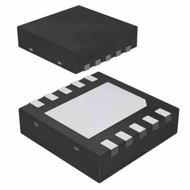
2.5 mm x 3 mm 10-pin VSON Package
Proximity Switches
Capacitive and Inductive Sensors
Digital Outputs
3 Description
The TIOS101(x) devices are configurable as highside, low-side or push-pull drivers. These devices are
capable of withstanding up to 1.2 kV (500 Ω) of IEC
61000-4-5 surge and feature integrated reverse
polarity protection.
A simple pin-programmable interface allows easy
interfacing to the controller circuits. The output current
limit can be configured using an external resistor.
Fault reporting and internal protection functions are
provided for under voltage, over circuit current and
over temperature.
Device Information
PACKAGE(1)
PART NUMBER
BODY SIZE (NOM)
TIOS101
TIOS1013
VSON (10)
2.50 mm x 3.00 mm
TIOS1015
(1)
For all available devices, see the orderable addendum at the
end of the data sheet.
TIO S101(x)
VCC_OUT
VCC
VOL TA GE
REGULATOR
0.1 µF
100 V
1 µF
10 V
IN
Sen sor
Front-End
EN
CONTROL
LOG IC
10 kŸ
OUT
DIA GNOSTICS
and
CONTROL
NFA UL T
CUR_OK
TMP_OK
PWR_OK
GND
ILIM_ADJ
R SET
Typical Application Diagram
An©IMPORTANT
NOTICEIncorporated
at the end of this data sheet addresses availability, warranty, changes, use in
safety-critical
applications,
Copyright
2021 Texas Instruments
Submit
Document
Feedback
intellectual property matters and other important disclaimers. PRODUCTION DATA.
Product Folder Links: TIOS101 TIOS1013 TIOS1015
1
�TIOS101, TIOS1013, TIOS1015
www.ti.com
SLLSEV6C – JULY 2017 – REVISED FEBRUARY 2021
Table of Contents
1 Features............................................................................1
2 Applications..................................................................... 1
3 Description.......................................................................1
4 Revision History.............................................................. 2
5 Pin Configuration and Functions...................................3
6 Specifications.................................................................. 4
6.1 Absolute Maximum Ratings........................................ 4
6.2 ESD Ratings............................................................... 4
6.3 Recommended Operating Conditions.........................4
6.4 Thermal Information....................................................5
6.5 Electrical Characteristics.............................................5
6.6 Switching Characteristics............................................6
6.7 Typical Characteristics................................................ 7
7 Parameter Measurement Information............................ 8
8 Detailed Description........................................................9
8.1 Overview..................................................................... 9
8.2 Functional Block Diagrams......................................... 9
8.3 Feature Description...................................................10
8.4 Device Functional Modes..........................................15
9 Application Information Disclaimer............................. 17
9.1 Application Information............................................. 17
9.2 Typical Application.................................................... 17
10 Power Supply Recommendations..............................21
11 Layout........................................................................... 22
11.1 Layout Guidelines................................................... 22
11.2 Layout Example...................................................... 22
12 Device and Documentation Support..........................23
12.1 Receiving Notification of Documentation Updates..23
12.2 Support Resources................................................. 23
12.3 Trademarks............................................................. 23
12.4 Electrostatic Discharge Caution..............................23
12.5 Glossary..................................................................23
4 Revision History
Changes from Revision B (June 2019) to Revision C (February 2021)
Page
• Added Functional Safety to the Features list ..................................................................................................... 1
Changes from Revision A (August 2018) to Revision B (June 2019)
Page
• Added device numbers TIOS1013 and TIOS1015 to the data sheet ................................................................ 1
• Changed all TIOS101-3 To: TIOS1013 and TIOS101-5 To: TIOS1015 ............................................................. 1
• Changed Feature From: Reverse Polarity Protection of up to 55 V on VCC To: Reverse Polarity Protection of
up to 60 V on VCC .............................................................................................................................................1
• Changed the Supply voltage values From: MIN = –55 V, MAX = 50 V To: MIN = –60 V, MAX = 60 V in the
Absolute Maximum Ratings ............................................................................................................................... 4
• Changed the Voltage difference Max value From: 55 V To: 60 V in the Absolute Maximum Ratings ............... 4
• Changed |55 V| To: |60 V| in the Leakage current Test Conditions in the Electrical Characteristics.................. 5
• Changed text From: "not exceed 55 V DC at any time." To: "not exceed 60 V DC at any time." in the Reverse
Polarity Protection section................................................................................................................................ 13
Changes from Revision * (July 2017) to Revision A (August 2018)
Page
• Changed the Thermal Information table values..................................................................................................5
2
Submit Document Feedback
Copyright © 2021 Texas Instruments Incorporated
Product Folder Links: TIOS101 TIOS1013 TIOS1015
�TIOS101, TIOS1013, TIOS1015
www.ti.com
SLLSEV6C – JULY 2017 – REVISED FEBRUARY 2021
5 Pin Configuration and Functions
VCC_IN/OUT
1
10
NFAULT
2
9
VCC
NC
3
8
OUT
IN
4
7
GND
EN
5
6
ILIM_ADJ
Thermal
Pad
NC
Not to scale
Figure 5-1. DMW Package, 10-Pin (VSON), Top View
Table 5-1. Pin Functions
PIN
NAME
NO.
I/O
DESCRIPTION
OUT
8
O
VCC
9
POWER
Supply voltage (24 V nominal)
GND
7
POWER
Device ground
EN
5
I
Driver enable input signal from the local controller. Logic low sets the OUT output at Hi-Z. Weak internal pulldown.
IN
4
I
Transmit data input from the local controller. No effect if EN is low. Logic high sets low-side switch. Logic low
sets high-side switch. Weak internal pull-up.
VCC_IN/OUT
1
POWER
ILIM_ADJ
6
I
NFAULT
NC
Thermal Pad
Switch output
3.3-V or 5-V linear regulator output; external 3.3-V or 5-V logic supply input for option without LDO.
Input for current limit adjustment. Connect resistor RSET between ILIM_ADJ and GND.
Fault indicator output signal to the microcontroller. A low level indicates either an over- current, an
undervoltage in supply or an overtemperature condition. Connect this pin via pull-up resistor to VCC_IN/OUT.
2
OPEN-DRAIN
3, 10
—
No internal connection.
—
—
Connect to GND plane for optimal thermal and electrical performance
Submit Document Feedback
Copyright © 2021 Texas Instruments Incorporated
Product Folder Links: TIOS101 TIOS1013 TIOS1015
3
�TIOS101, TIOS1013, TIOS1015
www.ti.com
SLLSEV6C – JULY 2017 – REVISED FEBRUARY 2021
6 Specifications
6.1 Absolute Maximum Ratings
over operating free-air temperature range (unless otherwise noted)(1) (2)
Supply voltage
MIN
MAX
UNIT
Steady state voltage for VCC and OUT
–60
60
V
Transient pulse width < 100 µs for VCC and OUT
–65
65
V
60
V
Voltage difference
|V(VCC) – V(OUT)|
Logic supply voltage (TIOS101)
VCC_IN
–0.3
6
V
Input logic voltage
IN, EN, ILIM_ADJ
–0.3
6
V
Output current
NFAULT
–5
5
mA
-55
170
°C
Storage temperature, Tstg
(1)
(2)
Stresses beyond those listed under Absolute Maximum Ratings may cause permanent damage to the device. These are stress ratings
only, which do not imply functional operation of the device at these or any other conditions beyond those indicated under
Recommended Operating Conditions. Exposure to absolute-maximum-rated conditions for extended periods may affect device
reliability.
All voltages are with reference to the GND pin, unless otherwise specified.
6.2 ESD Ratings
VALUE
V(ESD)
Electrostatic discharge
Human-body model (HBM), per ANSI/ESDA/JEDEC
All pins
JS-001(1)
±4000
Contact discharge, per IEC 61000-4-2(2) (3)
±16000
Electrical fast transient, per IEC
61000-4-4(2)
Surge protection with 500 Ω, per IEC 61000-4-5;
1.2/50 μs (2)
(1)
(2)
(3)
Pins VCC, OUT
and GND
UNIT
V
±4000
±1200
JEDEC document JEP155 states that 500-V HBM allows safe manufacturing with a standard ESD control process.
Minimum 100-nF capacitor is required between VCC and GND. Minimum 1-µF capacitor is required between VCC_IN/OUT and GND.
Passing level is ±4500 V if the device is powered and EN=IN=HIGH.
6.3 Recommended Operating Conditions
over operating free-air temperature range (unless otherwise noted)
4
V(VCC)
Supply voltage
V(VCC_IN)
Logic level input voltage (TIOS101 only)
RSET
External resistor for OUT current limit
1/tBIT
Signaling rate (push-pull mode)
MIN
NOM
MAX
7
24
36
V
3
3.3
3.6
V
4.5
5
5.5
V
3.3 V configuration
5 V configuration
I(VCC_OUT)
LDO output current (TIOS1013 and TIOS1015 only)
TA
Operating ambient temperature
TJ
Junction temperature
0
–40
Submit Document Feedback
UNIT
100
kΩ
250
kbps
20
mA
125
°C
150
°C
Copyright © 2021 Texas Instruments Incorporated
Product Folder Links: TIOS101 TIOS1013 TIOS1015
�TIOS101, TIOS1013, TIOS1015
www.ti.com
SLLSEV6C – JULY 2017 – REVISED FEBRUARY 2021
6.4 Thermal Information
TIOS101(x)
THERMAL METRIC(1)
UNIT
DMW (10 Pins)
RθJA
Junction-to-ambient thermal resistance
68.1
°C/W
RθJC(top)
Junction-to-case (top) thermal resistance
60.1
°C/W
RθJB
Junction-to-board thermal resistance
40.6
°C/W
ψJT
Junction-to-top characterization parameter
13.4
°C/W
ψJB
Junction-to-board characterization parameter
40.7
°C/W
RθJC(bot)
Junction-to-case (bottom) thermal resistance
25.2
°C/W
(1)
For more information about traditional and new thermal metrics, see the Semiconductor and IC Package Thermal Metrics application
report.
6.5 Electrical Characteristics
over operating free-air temperature range (unless otherwise noted)
PARAMETER
TEST CONDITIONS
MIN
TYP
MAX
UNIT
EN = LOW, no load
1.5
2.2
mA
EN = HIGH, no load
2
2.7
mA
0.8
V
POWER SUPPLIES (VCC)
I(VCC)
Quiescent supply current
LOGIC-LEVEL INPUTS (EN, IN)
VIL
Input logic low voltage
VIH
Input logic high voltage
RPD
Pull-down (EN) resistance
2
100
kΩ
V
RPU
Pull-up (IN) resistance
200
kΩ
CONTROL OUTPUT (NFAULT)
VOL
Output logic low voltage
IO = 4 mA
0.5
V
IOZ
Output high impedance leakage
Output in Hi-Z, VO = 0 V or VCC_IN/OUT
1
µA
I = 250 mA
1.75
V
I = 200 mA
1.5
V
I = 100 mA
1.1
V
I = 250 mA
1.75
V
I = 200 mA
1.5
V
I = 100 mA
1.1
V
µA
–1
DRIVER OUTPUT (OUT)
High-side driver residual voltage
VDS(ON)
Low-side driver residual voltage
IP
IO(LIM)
OUT pull-up/down current
Driver output current limit
EN = LOW, IN = LOW, pull-down current
40
50
80
EN = LOW, IN = HIGH, pull-up current
40
50
80
µA
RSET = 100 kΩ
35
50
70
mA
RSET = 0 kΩ
300
350
400
mA
RSET = OPEN(1)
300
350
400
mA
PROTECTION CIRCUITS
V(UVLO)
VCC under voltage lockout
V(UVLO,HYS
VCC under voltage hysteresis
)
V(UVLO_IN)
VCC falling; NFAULT = Hi-Z
6
V
VCC rising; NFAULT = LOW
6.5
V
Rising to falling threshold
100
VCC_IN under voltage lockout (No VCC_IN falling; NFAULT = Hi-Z
LDO option)
VCC_IN rising; NFAULT = LOW
V(UVLO,HYS VCC_IN under voltage hysteresis
(No LDO option)
)
T(WRN)
Thermal warning
T(SDN)
Thermal shutdown
T(HYS)
Thermal hysteresis for shutdown
Rising to falling threshold
mV
2.4
V
2.5
V
100
mV
125
Die temperature TJ
150
°C
160
°C
10
°C
Submit Document Feedback
Copyright © 2021 Texas Instruments Incorporated
Product Folder Links: TIOS101 TIOS1013 TIOS1015
5
�TIOS101, TIOS1013, TIOS1015
www.ti.com
SLLSEV6C – JULY 2017 – REVISED FEBRUARY 2021
6.5 Electrical Characteristics (continued)
over operating free-air temperature range (unless otherwise noted)
PARAMETER
IREV
TEST CONDITIONS
MIN
TYP
MAX
UNIT
V(OUT) < V(VCC) or
V(OUT) > V(VCC)
up to |36 V|
50
µA
V(OUT) < V(OUT) or
Leakage current in reverse polarity V(OUT) > V(VCC)
up to |60 V|
80
µA
550
µA
10
µA
EN = HIGH, IN = LOW; V(OUT to VCC) = 3 V
EN = HIGH, IN = HIGH; V(OUT to GND) = -3 V
LINEAR REGULATOR (LDO)
V(VCC_OUT) Voltage regulator output
TIOS1015
4.75
5
5.25
V
TIOS1013
3.13
3.3
3.46
V
TIOS1015
1.9
V
TIOS1013
2.3
V
mV/V
V(DROP)
Voltage regulator drop-out voltage
(V(VCC) – V(VCC_OUT))
ICC = 20 mA load current
REG
Line regulation (dV(VCC_OUT)/
dV(VCC)
I(VCC_OUT) = 1 mA
1.7
LREG
Load regulation (dV(VCC_OUT)/
V(VCC_OUT))
V(VCC) = 24 V, I(VCC_OUT) = 100 µA to 20 mA
1%
PSSR
Power Supply Rejection Ratio
100 kHz, I(VCC_OUT) = 20 mA
(1)
40
dB
Current fault indication will be active. Current fault auto recovery will be de-activated.
6.6 Switching Characteristics
over operating free-air temperature range (unless otherwise noted)
PARAMETER
Driver propagation delay
tP(skew)
Driver propagation delay skew. |tPLH tPHL|
tPZH, tPZL
Driver enable delay
tPHZ, tPLZ
Driver disable delay
tr, tf
Driver output rise, fall time
|tr – tf|
Difference in rise and fall time
tSC
Current fault blanking time
tpSC
Current fault indication delay
tSCEN
Current fault driver re-enable wait time
t(UVLO)
(1)
6
TEST CONDITIONS
tPLH, tPHL
OUT re-enable delay after UVLO
MIN
See Figure 7-1
See Figure 7-2
See Figure 7-3
RL = 2 kΩ
CL = 5 nF
R(SET) = 0 Ω
TYP
MAX
UNIT
600
800
ns
100
175
ns
4
µs
4
µs
150
ns
50
ns
200
µs
260
(1)
15
V(UVLO) rising threshold crossing
time to OUT enable time
10
30
µs
ms
50
ms
OUT output remains Hi-Z for this time
Submit Document Feedback
Copyright © 2021 Texas Instruments Incorporated
Product Folder Links: TIOS101 TIOS1013 TIOS1015
�TIOS101, TIOS1013, TIOS1015
www.ti.com
SLLSEV6C – JULY 2017 – REVISED FEBRUARY 2021
6.7 Typical Characteristics
3
1.8
1.6
2.5
Residual Voltage (V)
Supply Current (mA)
1.4
2
1.5
1
1.2
1
0.8
0.6
0.4
0.5
EN = High
EN = Low
-40qC
25qC
125qC
0.2
0
0
0
5
10
No load
15
20
25
Supply Voltage (V)
30
35
40
0
50
D001
IN = OPEN
25°C
100
150
Load Current (mA)
200
250
D002
Figure 6-2. Residual Voltage vs Load Current: High Side
1.6
400
1.4
350
1.2
300
1
250
IO(LIM) (mA)
Residual Voltage (V)
Figure 6-1. Supply Current vs Supply Voltage
0.8
0.6
0.4
Low Side
High Side
200
150
100
-40qC
25qC
125qC
0.2
50
0
0
0
50
100
150
Load Current (mA)
200
250
0
20
D003
Figure 6-3. Residual Voltage vs Load Current: Low Side
40
60
RSET (k:)
80
100
D004
Figure 6-4. Current Limit vs RSET
Submit Document Feedback
Copyright © 2021 Texas Instruments Incorporated
Product Folder Links: TIOS101 TIOS1013 TIOS1015
7
�TIOS101, TIOS1013, TIOS1015
www.ti.com
SLLSEV6C – JULY 2017 – REVISED FEBRUARY 2021
7 Parameter Measurement Information
VCC
RL
IN
OUT
RL
CL
EN
Figure 7-1. Test Circuit for Driver Switching
VOH
VOH
80%
80%
50%
IN
tPHL
OUT
tPHL
OUT
VOH
50%
20%
20%
OUT
VOL
VOL
VOL
tr
tf
Figure 7-2. Waveforms for Driver Output Switching Measurements
IN = Low
IN = High
50%
50%
EN
EN
tPLZ
tPLZ
tPZH
tPHZ
VVCC/2
VOH
50%
20%
OUT
VOL
OUT
80%
50%
VVCC/2
Figure 7-3. Waveforms for Driver Enable or Disable Time Measurements
8
Submit Document Feedback
Copyright © 2021 Texas Instruments Incorporated
Product Folder Links: TIOS101 TIOS1013 TIOS1015
�TIOS101, TIOS1013, TIOS1015
www.ti.com
SLLSEV6C – JULY 2017 – REVISED FEBRUARY 2021
8 Detailed Description
8.1 Overview
Figure 8-1 shows that the device driver output (OUT) can be used in a push-pull, high-side, or low-side
configuration using the enable (EN) and transmit data (IN) input pins. OUT can drive resistive, large capacitive or
large inductive loads.
TIOS101 and TIOS101x devices have integrated IEC 61000-4-4/5 EFT and surge protection. In addition,
tolerance to ±65-V transients enables flexibility to choose from a wider range of TVS diodes if an application
requires higher levels of protection. These integrated robustness features will simplify the system-level design by
reducing the external protection circuitry.
These devices implement protection features for over-current, over-voltage and over-temperature conditions.
The devices also provide a current-limit setting of the driver output current using an external resistor.
The TIOS101x devices derive the low voltage supply from the typical 24 V industrial supply via an internal linear
regulator to provide power to the local controller and sensor circuitry.
8.2 Functional Block Diagrams
VCC
VCC_IN
Control
Logic
IN
EN
OUT
Diagnostics
& Control
NFAULT
CUR_OK
TMP_OK
PWR_OK
GND
ILIM_ADJ
Figure 8-1. Block Diagram, TIOS101
Voltage
Regulator
VCC_OUT
Control
Logic
IN
EN
VCC
OUT
Diagnostics
& Control
NFAULT
CUR_OK
TMP_OK
PWR_OK
GND
ILIM_ADJ
Figure 8-2. Block Diagram, TIOS101x
Submit Document Feedback
Copyright © 2021 Texas Instruments Incorporated
Product Folder Links: TIOS101 TIOS1013 TIOS1015
9
�TIOS101, TIOS1013, TIOS1015
www.ti.com
SLLSEV6C – JULY 2017 – REVISED FEBRUARY 2021
8.3 Feature Description
8.3.1 Current Limit Configuration
The output current can be configured with an internal resistor on ILIM_ADJ pin. The maximum settable current
limit is 300 mA. This maximum setting specifies a minimum of 300 mA over temperature and voltage.
Output disable due to current fault and current fault auto recovery features can be disabled by floating ILIM_ADJ
pin. However, the current fault indication is still active in this configuration. This feature is useful when driving
large capacitances.
Table 8-1. Current Limitation
ILIM_ADJ Pin Condition
OUT Current Limit
NFAULT Indication During Fault
Output Disable and Auto
Recovery
RSET resistor to GND
Variable
Yes
Yes
Connected to GND
300 mA
Yes
Yes
OPEN
300 mA
Yes
No
8.3.2 Current Fault Detection, Indication and Auto Recovery
If the output current at OUT exceeds the internally set current limit IO(LIM) for a duration longer than tSC, the
NFAULT pin is driven logic low to indicate a fault condition. The output is turned off, but the LDO continues to
function. The output periodically retries to check if the output is still in the over current condition. In this mode,
the output is switched on for tSC in tSCEN intervals. Current fault auto recovery mode can be disabled by setting
ILIM_ADJ = OPEN. See Table 8-3.Toggling EN will clear NFAULT.
8.3.3 Thermal Warning, Thermal Shutdown
If the die temperature exceeds T(WRN), the NFAULT flag is held low indicating a potential over temperature
problem. When the TJ exceeds T(SDN), The output is disabled but the LDO remains operational. As soon as the
temperature drops below the temperature threshold (and after T(HYS)), the internal circuit re-enables the driver,
subject to the state of the EN and IN pins.
10
Submit Document Feedback
Copyright © 2021 Texas Instruments Incorporated
Product Folder Links: TIOS101 TIOS1013 TIOS1015
�TIOS101, TIOS1013, TIOS1015
www.ti.com
SLLSEV6C – JULY 2017 – REVISED FEBRUARY 2021
8.3.4 Fault Reporting (NFAULT)
NFAULT is driven low if either a current fault condition is detected, die temperature has exceeded T(WRN) or
supply has dropped below the UVLO threshold. NFAULT returns to high-impedance as soon as all three fault
conditions clear.
&
EN
*
EN
Current
Fault
T >TWRN
CUR_OK = L
Driver = OFF
LDO= ON
t= tSCEN
T < (TSD + THYS)
Out at IO(LIM) and T < TWRN
OUT NOT at IO(LIM)
T > TWRN
T < TWRN & EN*
T<
RN
TW
RN
TW
OUT at IO(LIM)
T>
CUR_OK = Z
TMP_OK = L
Driver= EN/EN*
LDO= ON
T > TSD
CUR_OK = Z
Driver = ON
LDO = ON
for t > tsc
Thermal
Warning
Normal
Operation
EN*
CUR_OK=Z
Driver = OFF
LDO = ON
OUT at IO(LIM)
Output at Hi-Z
Current
Fault Recovery
Thermal
Shutdown
CUR_OK = L
CUR_OK = Z
TMP_OK = L
Driver = OFF
LDO = ON
Driver = ON for tsc
LDO= ON
NFAULT = [CUR_OK && PWR_OK && TMP_OK]
Figure 8-3. Device State Diagram
Submit Document Feedback
Copyright © 2021 Texas Instruments Incorporated
Product Folder Links: TIOS101 TIOS1013 TIOS1015
11
�TIOS101, TIOS1013, TIOS1015
www.ti.com
SLLSEV6C – JULY 2017 – REVISED FEBRUARY 2021
8.3.5 Device Function Tables
Table 8-2. Driver Function
EN
IN
OUT
COMMENT
L / Open
X
Hi-Z
H
L
H
OUT is sourcing current (high-side drive)
H
H / Open
L
OUT is sinking current (low-side drive)
Device is in ready-to-receive state
Table 8-3. Current Limit Indicator Function (t > tSC)
EN
IN
H
H / Open
H
L
L / Open
X
OUT CURRENT
NFAULT
COMMENT
| I(OUT) | > IO(LIM)
L
OUT current exceeds the set limit for over tSC
| I(OUT) | < IO(LIM)
Z
Normal operation
| I(OUT) | > IO(LIM)
L
OUT current exceeds the set limit for over tSC
| I(OUT) | < IO(LIM)
Z
Normal operation
X
Z
Driver is disabled, current limit indicator is inactive
8.3.6 The Integrated Voltage Regulator (LDO)
The TIOS1013 and TIOS1015 each have an integrated linear voltage regulator (LDO) which can supply power to
external components. The voltage regulator is specified for VCC voltages in the range of 7 V to 36 V with respect
to GND. The LDO is capable of delivering up to 20 mA. The LDO output is current limited to 35-mA to limit the
inrush current onto VCC_OUT decoupling capacitors during initial power up.
The LDO is designed to be stable with standard ceramic capacitors with values of 1 μF or larger at the output.
X5R- and X7R-type capacitors are best because they have minimal variation in value and ESR over
temperature. Maximum ESR should be less than 1 Ω. With tolerance and dc bias effects, the minimum
capacitance to ensure stability is 1 μF.
12
Submit Document Feedback
Copyright © 2021 Texas Instruments Incorporated
Product Folder Links: TIOS101 TIOS1013 TIOS1015
�TIOS101, TIOS1013, TIOS1015
www.ti.com
SLLSEV6C – JULY 2017 – REVISED FEBRUARY 2021
8.3.7 Reverse Polarity Protection
Reverse polarity protection circuitry protects the devices against accidental reverse polarity connections to the
VCC, OUT and GND pins. The maximum voltage between any of the pins may not exceed 60 V DC at any time.
Figure 8-4 and Figure 8-5 shows all the possible connection combinations.
VCC
VCC
DC
OUT
TIOS101(x)
OUT
DC
TIOS101(x)
RL
GND
RL
GND
Correct
Configuration
Reverse Polarity Prot ected
Fault Conditions
VCC
VCC
DC
OUT
TIOS101(x)
GND
RL
OUT
TIOS101(x)
GND
DC
RL
Reverse Polarity Prot ected
Reverse Polarity Prot ected
Fault Conditions
Fault Conditions
VCC
TIOS101(x)
VCC
DC
OUT
RL
GND
OUT
DC
TIOS101(x)
GND
RL
Reverse Polarity Prot ected
Reverse Polarity Prot ected
Fault Conditions
Fault Conditions
Figure 8-4. High-Side Driver Configuration
Submit Document Feedback
Copyright © 2021 Texas Instruments Incorporated
Product Folder Links: TIOS101 TIOS1013 TIOS1015
13
�TIOS101, TIOS1013, TIOS1015
www.ti.com
SLLSEV6C – JULY 2017 – REVISED FEBRUARY 2021
VCC
VCC
DC
OUT
TIOS101(x)
DC
OUT
TIOS101(x)
RL
RL
GND
GND
Reverse Polarity Prot ected
Fault Conditions
Correct
Configuration
VCC
VCC
DC
OUT
TIOS101(x)
DC
OUT
TIOS101(x)
RL
RL
GND
GND
Reverse Polarity Prot ected
Fault Conditions
Reverse Polarity Prot ected
Fault Conditions
VCC
VCC
TIOS101(x)
DC
OUT
TIOS101(x)
DC
OUT
RL
RL
GND
GND
Reverse Polarity Prot ected
Fault Conditions
Reverse Polarity Prot ected
Fault Conditions
Figure 8-5. Low-Side Driver Configuration
14
Submit Document Feedback
Copyright © 2021 Texas Instruments Incorporated
Product Folder Links: TIOS101 TIOS1013 TIOS1015
�TIOS101, TIOS1013, TIOS1015
www.ti.com
SLLSEV6C – JULY 2017 – REVISED FEBRUARY 2021
8.3.8 Integrated Surge Protection and Transient Waveform Tolerance
The VCC and OUT pins of the device are capable of withstanding up to 1.2 kV of 1.2/50 – 8/20 μs IEC
61000-4-5 surge with a source impedance of 500 Ω. The surge testing should be performed with a minimum 100
nF supply decoupling capacitor between VCC and GND, and 1 µF between VCC_IN/OUT and GND.
External TVS diodes may be required for higher transient protection levels. The system designer should ensure
that the maximum clamping voltage of the external diodes should be < 65 V at the desired current level. The
device is capable of withstanding up to ±65-V transient pulses < 100 µs.
Combination
Wave
Generator
R
Protection
Equipment
Auxiliary
Equipment
EUT
VCC
OUT
Decoupling
Network
>100nF
GND
1.2/50 - 80/20 µs CWG
R = 500 Ω
Figure 8-6. Surge Test Setup
8.3.9 Power Up Sequence
VCC_IN and VCC domains can be powered up in any sequence. In the event of VCC is powered and VCC_IN is
not, the OUT pin remains in high impedance.
8.3.10 Undervoltage Lock-Out (UVLO)
The device enters UVLO if the VCC voltage falls below V(UVLO). (For the device without the integrated LDO, the
device monitors VCC_IN in addition to VCC. UVLO happens if either supply falls below the threshold.)
As soon as the supply falls below V(UVLO), NFAULT is pulled low, the LDO is turned off and the OUT output is
disabled (Hi-Z). Receiver performance is not specified in this mode.
When the supply rises above V(UVLO), NFAULT returns to Hi-Z (given no other fault conditions present) and the
LDO will be enabled immediately. The OUT output will be turned on after T(UVLO) delay.
8.4 Device Functional Modes
These devices can operate in three different modes.
8.4.1 NPN Configuration (N-Switch Mode)
Set IN pin high (or open) and use EN pin as control for realizing the function of an N-switch (low-side
configuration) on OUT.
8.4.2 PNP Configuration (P-Switch Mode)
Set IN pin low and use EN pin as control for realizing the function of a P-switch (high-side configuration) on OUT.
8.4.3 Push-Pull Mode
Set EN pin high and toggle IN as control for realizing the function of a push-pull output on OUT. Table 8-4, Table
8-5, and Table 8-6 summarize the pin configurations to accomplish the functional modes.
Submit Document Feedback
Copyright © 2021 Texas Instruments Incorporated
Product Folder Links: TIOS101 TIOS1013 TIOS1015
15
�TIOS101, TIOS1013, TIOS1015
www.ti.com
SLLSEV6C – JULY 2017 – REVISED FEBRUARY 2021
Table 8-4. NPN Mode
EN
IN
OUT
L / Open
H / Open
Hi-Z
H
H / Open
N-Switch
Table 8-5. PNP Mode
EN
IN
OUT
L / Open
L
Hi-Z
H
L
P-Switch
Table 8-6. Push-Pull Mode
EN
16
IN
OUT
L / Open
X
Hi-Z
H
H / Open
N-Switch
H
L
P-Switch
Submit Document Feedback
Copyright © 2021 Texas Instruments Incorporated
Product Folder Links: TIOS101 TIOS1013 TIOS1015
�TIOS101, TIOS1013, TIOS1015
www.ti.com
SLLSEV6C – JULY 2017 – REVISED FEBRUARY 2021
9 Application Information Disclaimer
Note
Information in the following applications sections is not part of the TI component specification, and TI
does not warrant its accuracy or completeness. TI’s customers are responsible for determining
suitability of components for their purposes, as well as validating and testing their design
implementation to confirm system functionality.
9.1 Application Information
TIOS101 and TIOS101x are robust 24-V digital drivers for industrial sensors.
9.2 Typical Application
TIO S101(x)
VCC_OUT
VCC
VOL TA GE
REGULATOR
0.1 µF
100 V
1 µF
10 V
IN
Sen sor
Front-End
EN
CONTROL
LOG IC
10 kŸ
OUT
DIA GNOSTICS
and
CONTROL
NFA UL T
CUR_OK
TMP_OK
PWR_OK
GND
ILIM_ADJ
R SET
Figure 9-1. Typical Application Schematic
9.2.1 Design Requirements
Table 9-1 shows recommended components for a typical system design.
Table 9-1. Design Parameters
PARAMETERS
VALUE
Input voltage range (VCC)
24 V, 30 V (max)
Output current (OUT)
200 mA
Output voltage (VCC_OUT), Pick TIOS1015
5V
Maximum LDO output current (IVCC(OUT))
5 mA
Pull-up resistors for NFAULT
10 kΩ
VCC decoupling capacitor
0.1 µF / 100 V
LDO output capacitor
1 µF / 10 V
ILIM_ADJ resistor (RSET)
10 kΩ
Maximum Ambient Temperature, TA
105°C
Submit Document Feedback
Copyright © 2021 Texas Instruments Incorporated
Product Folder Links: TIOS101 TIOS1013 TIOS1015
17
�TIOS101, TIOS1013, TIOS1015
www.ti.com
SLLSEV6C – JULY 2017 – REVISED FEBRUARY 2021
9.2.2 Detailed Design Procedure
9.2.2.1 Maximum Junction Temperature Check
For a 200 mA current limit:
• The maximum driver output current limit, IO(LIM) = 250 mA (allowed for current limit tolerance).
• The maximum voltage drop across the high-side switch is given with VDS(ON) = 1.75 V.
This causes a power consumption of:
2&12 = 8&5(10) T +1(.+/) = 1.758 T 250 I# = 437.5 I9
(1)
For a 5 mA LDO current output,
2&.&1 = k8.+ F 88%%_176 o x +8%%_176 = :30 F 5;V x 5 mA = 125 mW
(2)
Total power dissipation,
2& = 2&12 + 2&.&1 = 437.5 I9 + 125 I9 = 562.5 I9
(3)
Multiply this value with the Junction-to-ambient thermal resistance of θJA = 68.1°C/W (taken from the Section 6.4
table) to receive the difference between junction temperature, TJ, and ambient temperature, TA:
¿6 = 6, F 6# = 2& x E,# = 562.5 I9 T 68.1°%/9 = 38.3°%
(4)
Add this value to the maximum ambient temperature of TA = 105°C to receive the final junction temperature:
6, FI=T = 6#FI=T + ¿6 = 105°% + 38.3°% = 143.3°%
(5)
As long as TJ-max is below the recommended maximum value of 150°C, no thermal shutdown will occur.
However, thermal warning may occur as the junction temperature is greater than TWRN.
Note that the modeling of the complete system may be necessary to predict junction temperature in smaller
PCBs and/or enclosures without air flow.
9.2.2.2 Driving Capacitive Loads
These devices are capable of driving capacitive loads on the OUT output. Assuming a pure capacitive load
without series/parallel resistance, the maximum capacitance that can be charged without triggering current fault
can be calculated as:
CLOAD
[IO LIM x t SC ]
V VCC
(6)
Higher capacitive loads can be driven if a series resistor is connected between the OUT and the load. Capacitive
loads can be connected to VCC and GND.
18
Submit Document Feedback
Copyright © 2021 Texas Instruments Incorporated
Product Folder Links: TIOS101 TIOS1013 TIOS1015
�TIOS101, TIOS1013, TIOS1015
www.ti.com
SLLSEV6C – JULY 2017 – REVISED FEBRUARY 2021
9.2.2.3 Driving Inductive Loads
The TIOS101(x) family is capable of magnetizing and demagnetizing inductive loads up to 1.5 H. These devices
contain internal circuitry that enables fast demagnetization when configured as either P-switch or N-switch mode.
In P-switch configuration, the load inductor L is magnetized when the OUT pin is driven high. When the PNP is
turned off, there is a significant amount of negative inductive kick back at the OUT pin. This voltage is clamped
internally at about -75 V.
Similarly in N-switch configuration, the load inductor L is magnetized when the OUT pin is driven low. When the
NPN is turned off, there is a significant amount of positive inductive kick back at the OUT pin. This voltage is
clamped internally at about 75 V.
The equivalent protection circuits are shown in Figure 9-2 and Figure 9-3. The minimum value of the resistive
load R can be calculated as:
R
V VCC
IO( LIM )
(7)
spacer
VCC
VCC
R
OUT
OUT
L
L
R
TIO S101(x)
Figure 9-3. NPN Mode
TIO S101(x)
Figure 9-2. PNP Mode
Submit Document Feedback
Copyright © 2021 Texas Instruments Incorporated
Product Folder Links: TIOS101 TIOS1013 TIOS1015
19
�TIOS101, TIOS1013, TIOS1015
www.ti.com
SLLSEV6C – JULY 2017 – REVISED FEBRUARY 2021
3 V/div
8 V/div
10 V/div
2 V/div
10 V/div
9.2.3 Application Curves
Time 10 ms/div
Time 1 Ps/div
Figure 9-5. OUT Power Up Delay, Low Side Mode
125 kHz
4 V/div
3 V/div
10 V/div
300 mA/div
10 V/div
800 mV/div
Figure 9-4. OUT in Push-Pull Mode
Time 50 Ps/div
Time 10 ms/div
Figure 9-7. OUT In Current Fault, Low Side Mode
4 V/div
4 V/div
300 mA/div
300 mA/div
6 V/div
6 V/div
Figure 9-6. OUT Power Up Delay, High Side Mode
Time 10 ms/div
Time 50 Ps/div
Figure 9-8. OUT In Current Fault, High Side Mode
20
Figure 9-9. OUT In Current Fault Auto Recovery,
Low Side Mode
Submit Document Feedback
Copyright © 2021 Texas Instruments Incorporated
Product Folder Links: TIOS101 TIOS1013 TIOS1015
�TIOS101, TIOS1013, TIOS1015
www.ti.com
3 V/div
4 V/div
40 V/div
300 mA/div
2 V/div
6 V/div
SLLSEV6C – JULY 2017 – REVISED FEBRUARY 2021
Time 10 ms/div
Time 10 ms/div
Figure 9-10. OUT In Current Fault Auto Recovery,
High Side Mode
1.5-H
Inductor
With =
100 Ω
RSET =
OPEN
3 V/div
40 V/div
2 V/div
Figure 9-11. OUT Driving, Low Side Mode
Time 10 ms/div
1.5-H Inductor
With = 100 Ω
RSET = OPEN
Figure 9-12. OUT Driving, High Side Mode
10 Power Supply Recommendations
The TIOS101 and TIOS101x are designed to operate from a 24-V nominal supply at VCC, which can vary by
+12 V and -17 V from the nominal value to remain within the device's recommended supply voltage range of 7 V
to 36 V. This supply should be buffered with at least a 100-nF/100-V capacitor.
Submit Document Feedback
Copyright © 2021 Texas Instruments Incorporated
Product Folder Links: TIOS101 TIOS1013 TIOS1015
21
�TIOS101, TIOS1013, TIOS1015
www.ti.com
SLLSEV6C – JULY 2017 – REVISED FEBRUARY 2021
11 Layout
11.1 Layout Guidelines
•
•
•
•
•
•
•
•
Use of a 4-layer board is recommended for good heat conduction. Use layer 1 (top layer) for control signals,
layer 2 as GND, layer 3 for the 24-V supply plane (VCC), and layer 4 for the regulated output supply
(VCC_IN/OUT).
Connect the thermal pad to GND with maximum amount of thermal vias for best thermal performance.
Use entire planes for VCC, VCC_IN/OUT and GND to assure minimum inductance.
The VCC terminal must be decoupled to ground with a low-ESR ceramic decoupling capacitor with a
minimum value of 100 nF. The capacitor must have a voltage rating of 50 V minimum (100 V depending on
max sensor supply fault rating) and an X5R or X7R dielectric.
• The optimum placement of the capacitor is closest to the VCC and GND terminals to reduce supply drops
during large supply current loads. See Figure 11-1 for a PCB layout example.
Connect all open-drain control outputs via 10 kΩ pull-up resistors to the VCC_IN/OUT plane to provide a
defined voltage potential to the system controller inputs when the outputs are high-impedance.
Connect the RSET resistor between ILIM_ADJ and GND.
Decouple the regulated output voltage at VCC_IN/OUT to ground with a low-ESR, 1 μF, ceramic decoupling
capacitor. The capacitor should have a voltage rating of 10 V minimum and an X5R or X7R dielectric.
11.2 Layout Example
VIA to Layer 2: Power Ground Plane (VCC)
VIA to Layer 3: 24V Supply Plane (GND)
VIA to Layer 4: Regulated Supply Plane (VCC_IN/OUT)
1uF/10V
VC
100nF/
50V
T
U
/O
N
_I
C
NFAULT
NC
VCC
VCC
NC
OUT
GND
EN
ILIM_ADJ
OUT
IN
Exposed Thermal
Pad Area
RSET
GND
Use Multiple Vias for
VCC and GND
Figure 11-1. Layout Example
22
Submit Document Feedback
Copyright © 2021 Texas Instruments Incorporated
Product Folder Links: TIOS101 TIOS1013 TIOS1015
�TIOS101, TIOS1013, TIOS1015
www.ti.com
SLLSEV6C – JULY 2017 – REVISED FEBRUARY 2021
12 Device and Documentation Support
12.1 Receiving Notification of Documentation Updates
To receive notification of documentation updates, navigate to the device product folder on ti.com. Click on
Subscribe to updates to register and receive a weekly digest of any product information that has changed. For
change details, review the revision history included in any revised document.
12.2 Support Resources
TI E2E™ support forums are an engineer's go-to source for fast, verified answers and design help — straight
from the experts. Search existing answers or ask your own question to get the quick design help you need.
Linked content is provided "AS IS" by the respective contributors. They do not constitute TI specifications and do
not necessarily reflect TI's views; see TI's Terms of Use.
12.3 Trademarks
TI E2E™ is a trademark of Texas Instruments.
All trademarks are the property of their respective owners.
12.4 Electrostatic Discharge Caution
This integrated circuit can be damaged by ESD. Texas Instruments recommends that all integrated circuits be handled
with appropriate precautions. Failure to observe proper handling and installation procedures can cause damage.
ESD damage can range from subtle performance degradation to complete device failure. Precision integrated circuits may
be more susceptible to damage because very small parametric changes could cause the device not to meet its published
specifications.
12.5 Glossary
TI Glossary
This glossary lists and explains terms, acronyms, and definitions.
Mechanical, Packaging, and Orderable Information
The following pages include mechanical, packaging, and orderable information. This information is the most
current data available for the designated devices. This data is subject to change without notice and revision of
this document. For browser-based versions of this data sheet, refer to the left-hand navigation.
Submit Document Feedback
Copyright © 2021 Texas Instruments Incorporated
Product Folder Links: TIOS101 TIOS1013 TIOS1015
23
�PACKAGE OPTION ADDENDUM
www.ti.com
2-Feb-2021
PACKAGING INFORMATION
Orderable Device
Status
(1)
Package Type Package Pins Package
Drawing
Qty
Eco Plan
(2)
Lead finish/
Ball material
MSL Peak Temp
Op Temp (°C)
Device Marking
(3)
(4/5)
(6)
TIOS1013DMWR
ACTIVE
VSON
DMW
10
1500
RoHS & Green
NIPDAU
Level-2-260C-1 YEAR
-40 to 125
TS1013
TIOS1013DMWT
ACTIVE
VSON
DMW
10
250
RoHS & Green
NIPDAU
Level-2-260C-1 YEAR
-40 to 125
TS1013
TIOS1015DMWR
ACTIVE
VSON
DMW
10
1500
RoHS & Green
NIPDAU
Level-2-260C-1 YEAR
-40 to 125
TS1015
TIOS1015DMWT
ACTIVE
VSON
DMW
10
250
RoHS & Green
NIPDAU
Level-2-260C-1 YEAR
-40 to 125
TS1015
TIOS101DMWR
ACTIVE
VSON
DMW
10
1500
RoHS & Green
NIPDAU
Level-2-260C-1 YEAR
-40 to 125
TS101
TIOS101DMWT
ACTIVE
VSON
DMW
10
250
RoHS & Green
NIPDAU
Level-2-260C-1 YEAR
-40 to 125
TS101
(1)
The marketing status values are defined as follows:
ACTIVE: Product device recommended for new designs.
LIFEBUY: TI has announced that the device will be discontinued, and a lifetime-buy period is in effect.
NRND: Not recommended for new designs. Device is in production to support existing customers, but TI does not recommend using this part in a new design.
PREVIEW: Device has been announced but is not in production. Samples may or may not be available.
OBSOLETE: TI has discontinued the production of the device.
(2)
RoHS: TI defines "RoHS" to mean semiconductor products that are compliant with the current EU RoHS requirements for all 10 RoHS substances, including the requirement that RoHS substance
do not exceed 0.1% by weight in homogeneous materials. Where designed to be soldered at high temperatures, "RoHS" products are suitable for use in specified lead-free processes. TI may
reference these types of products as "Pb-Free".
RoHS Exempt: TI defines "RoHS Exempt" to mean products that contain lead but are compliant with EU RoHS pursuant to a specific EU RoHS exemption.
Green: TI defines "Green" to mean the content of Chlorine (Cl) and Bromine (Br) based flame retardants meet JS709B low halogen requirements of


 工商网监
湘ICP备2023018690号
工商网监
湘ICP备2023018690号
