�������� ��������
����
����� �
������ �
���
������ �����
������� ����
��
SLVS423 A− MAY 2002 − REVISED SEPTEMBER 2002
D
D
D
D
D
D
D
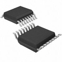
D, N OR PW PACKAGE
(TOP VIEW)
Two Complete PWM Control Circuits
Outputs Drive MOSFETs Directly
Oscillator Frequency . . . 50 kHz to 2 MHz
3.6-V to 20-V Supply-Voltage Range
Low Supply Current . . . 3.5 mA Typ
Adjustable Dead-Time Control, 0% to 100%
1.26-V Reference
CT
RT
DTC1
IN1 +
IN1 −
COMP1
GND
OUT1
description
1
16
2
15
3
14
4
13
5
12
6
11
7
10
8
9
REF
SCP
DTC2
IN2 +
IN2 −
COMP2
VCC
OUT2
The TL1454A is a dual-channel pulse-width-modulation (PWM) control circuit, primarily intended
for low-power, dc/dc converters. Applications
include LCD displays, backlight inverters, notebook computers, and other products requiring
small, high-frequency, dc/dc converters.
Each PWM channel has its own error amplifier, PWM comparator, dead-time control comparator, and MOSFET
driver. The voltage reference, oscillator, undervoltage lockout, and short-circuit protection are common to both
channels.
Channel 1 is configured to drive n-channel MOSFETs in step-up or flyback converters, and channel 2 is
configured to drive p-channel MOSFETs in step-down or inverting converters. The operating frequency is set
with an external resistor and an external capacitor, and dead time is continuously adjustable from 0 to 100%
duty cycle with a resistive divider network. Soft start can be implemented by adding a capacitor to the dead-time
control (DTC) network. The error-amplifier common-mode input range includes ground, which allows the
TL1454A to be used in ground-sensing battery chargers as well as voltage converters.
AVAILABLE OPTIONS
PACKAGED DEVICES†
TA
SMALL OUTLINE
(D)
PLASTIC DIP
(N)
TSSOP
(PW)
SSOP
(DB)
SOP-EIAJ
(NS)
CHIP FORM
(Y)
−20°C to 85°C
TL1454ACD
TL1454ACN
TL1454ACPWR
TL1454ACDB
TL1454ACNS
TL1454AY
† The D, DB and NS packages are available taped and reeled. Add the suffix R to the device name (e.g., TL1454ACDR). The PW package is
available only left-end taped and reeled (indicated by the R suffix on the device type; e.g., TL1454ACPWR).
Copyright 2002, Texas Instruments Incorporated
���
����� ��� �������!��� �" #$��%�! �" �� &$'(�#�!��� )�!%*
���)$#!" #������ !� "&%#���#�!���" &%� !+% !%��" �� �%,�" ��"!�$�%�!"
"!��)��) -�����!.* ���)$#!��� &��#%""��/ )�%" ��! �%#%""���(. ��#($)%
!%"!��/ �� �(( &����%!%�"*
POST OFFICE BOX 655303
• DALLAS, TEXAS 75265
1
��������� ��������
����
����� �
������ �
���
������ �����
������� ����
��
SLVS423 A− MAY 2002 − REVISED SEPTEMBER 2002
functional block diagram
VCC
10
Voltage
REF
GND
COMP1
IN1 +
IN1 −
RT CT
2
1
1.26 V
2.5 V
7
16
To Internal
Circuitry
1.2 V
OSC
5
VCC
PWM
Comparator 1
6
4
REF
1.8 V
+
_
8
OUT1
Error
Amplifier 1
PWM
Comparator 2
COMP2 11
13
+
IN2 +
12 _
IN2 −
Error
Amplifier 2
VCC
UVLO
and
SCP Latch
9
SCP
Comparator 2
1V
1V
SCP
Comparator 1
0.65 V
0.65 V
1.27 V
15
SCP
2
POST OFFICE BOX 655303
3
14
DTC1 DTC2
• DALLAS, TEXAS 75265
OUT2
��������� ��������
����
����� �
������ �
���
������ �����
������� ����
��
SLVS423 A− MAY 2002 − REVISED SEPTEMBER 2002
TL1454AY chip information
This device, when properly assembled, displays characteristics similar to the TL1454AC. Thermal compression
or ultrasonic bonding may be used on the doped aluminum bonding pads. The chips may be mounted with
conductive epoxy or a gold-silicon preform.
BONDING PAD ASSIGNMENTS
(15)
(14)
(13) (12)
(11)
(10)
(9)
(16)
86
(8)
(1)
(2)
(4)
(3)
(5)
(6)
(7)
108
CT
RT
DTC1
IN1 +
IN1−
COMP1
GND
OUT1
(1)
(16)
(2)
(15)
(3)
(14)
(4)
(13)
(5)
TL1454AY
(12)
(6)
(11)
(7)
(10)
(8)
(9)
REF
SCP
CHIP THICKNESS: 15 TYPICAL
DTC2
BONDING PADS: 4 × 4 MINIMUM
IN2+
TJmax = 150°C
IN2 −
TOLERANCES ARE ± 10%.
COMP2
ALL DIMENSIONS ARE IN MILS.
VCC
OUT2
POST OFFICE BOX 655303
• DALLAS, TEXAS 75265
3
��������� ��������
����
����� �
������ �
���
������ �����
������� ����
��
SLVS423 A− MAY 2002 − REVISED SEPTEMBER 2002
theory of operation
reference voltage
A linear regulator operating from VCC generates a 2.5-V supply for the internal circuits and the 1.26-V reference,
which can source a maximum of 1 mA for external loads. A small ceramic capacitor (0.047 µF to 0.1 µF) between
REF and ground is recommended to minimize noise pickup.
error amplifier
The error amplifier generates the error signal used by the PWM to adjust the power-switch duty cycle for the
desired converter output voltage. The signal is generated by comparing a sample of the output voltage to the
voltage reference and amplifying the difference. An external resistive divider connected between the converter
output and ground, as shown in Figure 1, is generally required to obtain the output voltage sample.
The amplifier output is brought out on COMP to allow the frequency response of the amplifier to be shaped with
an external RC network to stabilize the feedback loop of the converter. DC loading on the COMP output is limited
to 45 µA (the maximum amplifier source current capability).
Figure 1 illustrates the sense-divider network and error-amplifier connections for converters with positive output
voltages. The divider network is connected to the noninverting amplifier input because the PWM has a phase
inversion; the duty cycle decreases as the error-amplifier output increases.
TL1454A
REF
COMP
Compensation
Network
R3
Converter
Output
IN −
IN +
VO
R1
_
To PWM
+
R2
Figure 1. Sense Divider/Error Amplifier
Configuration for Converters with Positive Outputs
The output voltage is given by:
V
O
+V
ref
ǒ1 ) R1
Ǔ
R2
where Vref = 1.26 V.
The dc source resistance of the error-amplifier inputs should be 10 kΩ or less and approximately matched to
minimize output voltage errors caused by the input-bias current. A simple procedure for determining appropriate
values for the resistors is to choose a convenient value for R3 (10 kΩ or less) and calculate R1 and R2 using:
R1 +
R2 +
4
R 3V
O
V –V
O ref
R 3V
V
O
ref
POST OFFICE BOX 655303
• DALLAS, TEXAS 75265
��������� ��������
����
����� �
������ �
���
������ �����
������� ����
��
SLVS423 A− MAY 2002 − REVISED SEPTEMBER 2002
error amplifier
R1 and R2 should be tight-tolerance (±1% or better) devices with low and/or matched temperature coefficients
to minimize output voltage errors. A device with a ±5% tolerance is suitable for R3.
REF
COMP
R2
Compensation
Network
IN −
IN +
R1
_
To PWM
+
R3
Converter
V
Output O
Figure 2. Sense Divider/Error Amplifier Configuration for Converters with Negative Outputs
Figure 2 shows the divider network and error-amplifier configuration for negative output voltages. In general,
the comments for positive output voltages also apply for negative outputs. The output voltage is given by:
V
R V
+ * 1 ref
O
R2
The design procedure for choosing the resistor value is to select a convenient value for R2 (instead of R3 in
the procedure for positive outputs) and calculate R1 and R3 using:
R V
R1 + * 2 O
V
ref
R3 +
R 1R 2
R1 ) R2
Values in the 10-kΩ to 20-kΩ range work well for R2. R3 can be omitted and the noninverting amplifier connected
to ground in applications where the output voltage tolerance is not critical.
oscillator
The oscillator frequency can be set between 50 kHz and 2 MHz with a resistor connected between RT and GND
and a capacitor between CT and GND (see Figure 3). Figure 6 is used to determine RT and CT for the desired
operating frequency. Both components should be tight-tolerance, temperature-stable devices to minimize
frequency deviation. A 1% metal-film resistor is recommended for RT, and a 10%, or better, NPO ceramic
capacitor is recommended for CT.
TL1454A
RT
CT
2
1
RT
CT
Figure 3. Oscillator Timing
POST OFFICE BOX 655303
• DALLAS, TEXAS 75265
5
��������� ��������
����
����� �
������ �
���
������ �����
������� ����
��
SLVS423 A− MAY 2002 − REVISED SEPTEMBER 2002
dead-time control (DTC) and soft start
The two PWM channels have independent dead-time control inputs so that the maximum power-switch duty
cycles can be limited to less then 100%. The dead-time is set with a voltage applied to DTC; the voltage is
typically obtained from a resistive divider connected between the reference and ground as shown in Figure 4.
Soft start is implemented by adding a capacitor between REF and DTC.
The voltage, VDT, required to limit the duty cycle to a maximum value is given by:
V
DT
+V
O(max)
ǒ
*D V
O(max)
*V
O(min)
Ǔ * 0.65
where VO(max) and VO(min) are obtained from Figure 9, and D is the maximum duty cycle.
Predicting the regulator startup or rise time is complicated because it depends on many variables, including:
input voltage, output voltage, filter values, converter topology, and operating frequency. In general, the output
will be in regulation within two time constants of the soft-start circuit. A five-to-ten millisecond time constant
usually works well for low-power converters.
The DTC input can be grounded in applications where achieving a 100% duty cycle is desirable, such as a buck
converter with a very low input-to-output differential voltage. However, grounding DTC prevents the
implementation of soft start, and the output voltage overshoot at power-on is likely to be very large. A better
arrangement is to omit RDT1 (see Figure 4) and choose RDT2 = 47 kΩ. This configuration ensures that the duty
cycle can reach 100% and still allows the designer to implement soft start using CSS.
16
REF
TL1454A
RDT1
CSS
DTC
RDT2
Figure 4. Dead-Time Control and Soft Start
PWM comparator
Each of the PWM comparators has dual inverting inputs. One inverting input is connected to the output of the
error amplifier; the other inverting input is connected to the DTC terminal. Under normal operating conditions,
when either the error-amplifier output or the dead-time control voltage is higher than that for the PWM triangle
wave, the output stage is set inactive (OUT1 low and OUT2 high), turning the external power stage off.
undervoltage-lockout (UVLO) protection
The undervoltage-lockout circuit turns the output circuit off and resets the SCP latch whenever the supply
voltage drops too low (to approximately 2.9 V) for proper operation. A hysteresis voltage of 200 mV eliminates
false triggering on noise and chattering.
short-circuit protection (SCP)
The TL1454A SCP function prevents damage to the power switches when the converter output is shorted to
ground. In normal operation, SCP comparator 1 clamps SCP to approximately 185 mV. When one of the
converter outputs is shorted, the error amplifier output (COMP) will be driven below 1 V to maximize duty cycle
and force the converter output back up. When the error amplifier output drops below 1 V, SCP comparator 1
releases SCP, and capacitor, CSCP, which is connected between SCP and GND, begins charging. If the
error-amplifier output rises above 1 V before CSCP is charged to 1 V, SCP comparator 1 discharges CSCP and
normal operation resumes. If CSCP reaches 1 V, SCP comparator 2 turns on and sets the SCP latch, which turns
off the output drives and resets the soft-start circuit. The latch remains set until the supply voltage is lowered
to 2 V or less, or CSCP is discharged externally.
6
POST OFFICE BOX 655303
• DALLAS, TEXAS 75265
��������� ��������
����
����� �
������ �
���
������ �����
������� ����
��
SLVS423 A− MAY 2002 − REVISED SEPTEMBER 2002
short-circuit protection (SCP) (continued)
The SCP time-out period must be greater than the converter start-up time or the converter will not start. Because
high-value capacitor tolerances tend to be ± 20% or more and IC resistor tolerances are loose as well, it is best
to choose an SCP time-out period 10-to-15 times greater than the converter startup time. The value of CSCP
may be determined using Figure 6, or it can be calculated using:
T
C SCP + SCP
80.3
where CSCP is in µF and TSCP is the time-out period in ms.
output stage
The output stage of the TL1454A is a totem-pole output with a maximum source/sink current rating of 40 mA
and a voltage rating of 20 V. The output is controlled by a complementary output AND gate and is turned on
(sourcing current for OUT1, sinking current for OUT2) when all the following conditions are met: 1) the oscillator
triangle wave voltage is higher than both the DTC voltage and the error-amplifier output voltage, 2) the
undervoltage-lockout circuit is inactive, and 3) the short-circuit protection circuit is inactive.
absolute maximum ratings over operating free-air temperature range (unless otherwise noted)†
Supply voltage, VCC (see Note 1) . . . . . . . . . . . . . . . . . . . . . . . . . . . . . . . . . . . . . . . . . . . . . . . . . . . . . . . . . . . . 23 V
Error amplifier input voltage: IN1+, IN1 −, IN2+, IN2 − . . . . . . . . . . . . . . . . . . . . . . . . . . . . . . . . . . . . . . . . . . . . 23 V
Output voltage: OUT1, OUT2 . . . . . . . . . . . . . . . . . . . . . . . . . . . . . . . . . . . . . . . . . . . . . . . . . . . . . . . . . . . . . . . . 20 V
Continuous output current: OUT1, OUT2 . . . . . . . . . . . . . . . . . . . . . . . . . . . . . . . . . . . . . . . . . . . . . . . . . . ± 200 mA
Peak output current: OUT1, OUT2 . . . . . . . . . . . . . . . . . . . . . . . . . . . . . . . . . . . . . . . . . . . . . . . . . . . . . . . . . . . . 1 A
Continuous total dissipation . . . . . . . . . . . . . . . . . . . . . . . . . . . . . . . . . . . . . . . . . . . See Dissipation Rating Table
Operating free-air temperature range, TA: C suffix . . . . . . . . . . . . . . . . . . . . . . . . . . . . . . . . . . . . −20°C to 85°C
Storage temperature range, Tstg . . . . . . . . . . . . . . . . . . . . . . . . . . . . . . . . . . . . . . . . . . . . . . . . . . . −65°C to 150°C
Lead temperature 1,6 mm (1/16 inch) from case for 10 seconds . . . . . . . . . . . . . . . . . . . . . . . . . . . . . . . 260°C
† Stresses beyond those listed under “absolute maximum ratings” may cause permanent damage to the device. These are stress ratings only, and
functional operation of the device at these or any other conditions beyond those indicated under “recommended operating conditions” is not
implied. Exposure to absolute-maximum-rated conditions for extended periods may affect device reliability.
NOTE 1: All voltage values are with respect to network GND.
DISSIPATION RATING TABLE
PACKAGE
TA ≤ 25°C
POWER RATING
DERATING FACTOR
ABOVE TA = 25°C
TA = 70°C
POWER RATING
TA = 85°C
POWER RATING
D
950 mW
7.6 mW/°C
608 mW
494 mW
DB
1000 mW
8.0 mW/°C
640 mW
520 mW
N
1250 mW
10.0 mW/°C
800 mW
650 mW
NS
1953 mW
15.6 mW/°C
1250 mW
1015 mW
PW
500 mW
4.0 mW/°C
320 mW
260 mW
POST OFFICE BOX 655303
• DALLAS, TEXAS 75265
7
��������� ��������
����
����� �
������ �
���
������ �����
������� ����
��
SLVS423 A− MAY 2002 − REVISED SEPTEMBER 2002
recommended operating conditions
Supply voltage, VCC
Error amplifier common-mode input voltage
MIN
MAX
3.6
20
UNIT
V
−0.2
1.45
V
Output voltage, VO
20
V
Output current, IO
± 40
mA
COMP source current
−45
µA
COMP sink current
100
µA
1
mA
Reference output current
COMP dc load resistance
100
kΩ
Timing capacitor, CT
10
Timing resistor, RT
5.1
100
kΩ
Oscillator frequency
50
2000
kHz
−20
85
°C
Operating free-air temperature, TA
TL1454AC
4000
pF
electrical characteristics over recommended operating free-air temperature range, VCC = 6 V,
fosc = 500 kHz (unless otherwise noted)
reference
TL1454A
PARAMETER
Vref
TEST CONDITIONS
Output voltage, REF
Input regulation
Output regulation
Output voltage change with temperature
IOS
Short-circuit output current
MIN
TYP
MAX
1.22
1.26
1.32
IO = 1 mA,
IO = 1 mA
TA = 25°C
VOC = 3.6 V to 20 V,
IO = 0.1 mA to 1 mA
IO = 1 mA
TA = TA(min) to 25°C,
IO = 1 mA
−12.5
TA = 25°C to 85°C,
Vref = 0 V
IO = 1 mA
−12.5
−2.5
12.5
1.20
1.34
2
UNIT
V
6
mV
1
7.5
mV
−1.25
12.5
30
mV
mA
undervoltage lockout (UVLO)
TL1454A
PARAMETER
VIT +
VIT −
Positive-going threshold voltage
Vhys
Hysteresis, VIT + − VIT −
TEST CONDITIONS
MIN
TYP
MAX
2.9
Negative-going threshold voltage
TA = 25
25°C
C
100
UNIT
V
2.7
V
200
mV
short-circuit protection (SCP)
TL1454A
PARAMETER
VIT
Vstby†
Input threshold voltage
VI(latched)
Latched-mode input voltage
VIT(COMP)
Comparator threshold voltage
TEST CONDITIONS
TA = 25°C
Standby voltage
MAX
0.93
1
1.07
V
140
185
230
mV
60
120
mV
COMP1, COMP2
POST OFFICE BOX 655303
• DALLAS, TEXAS 75265
UNIT
TYP
No pullup
Input source current
TA = 25°C,
VO(SCP) = 0
† This symbol is not presently listed within EIA / JEDEC standards for semiconductor symbology.
8
MIN
1
−5
−15
V
−20
µA
��������� ��������
����
����� �
������ �
���
������ �����
������� ����
��
SLVS423 A− MAY 2002 − REVISED SEPTEMBER 2002
electrical characteristics over recommended operating free-air temperature range, VCC = 6 V,
fosc = 500 kHz (unless otherwise noted) (continued)
oscillator
TL1454A
PARAMETER
fosc
TEST CONDITIONS
Frequency
CT = 120 pF,
RT = 10 kΩ
VCC = 3.6 V to 20 V,
TA = TA(min) to 25°C
TA = 25°C
MIN
Standard deviation of frequency
Frequency change with voltage
Frequency change with temperature
TYP
MAX
500
kHz
50
kHz
10
TA = 25°C to 85°C
UNIT
kHz
−2
± 30
−10
± 30
kHz
Maximum ramp voltage
1.8
V
Minimum ramp voltage
1.1
V
dead-time control (DTC)
TL1454A
PARAMETER
VIT
Input threshold voltage
VI(latched)
IIB
Latched-mode input voltage
TEST CONDITIONS
MIN
TYP
MAX
Duty cycle = 0%
0.98
1.1
1.22
Duty cycle = 100%
0.38
0.5
0.62
1.2
Common-mode input bias current
DTC1, IN1+ ≈ 1.2 V
Latched-mode (source) current
TA = 25°C
UNIT
V
V
4
µA
µA
−100
error-amplifier
TL1454A
PARAMETER
VIO
IIO
Input offset voltage
IIB
VICR
Input bias current
AV
Open-loop voltage gain
Input offset current
Input voltage range
TEST CONDITIONS
VO = 1.25 V,
MIN
TYP
VIC = 1.25 V
−160
VCC = 3.6 V to 20 V
RFB = 200 kΩ
70
nA
nA
V
3
MHz
dB
Common-mode rejection ratio
60
80
Positive output voltage swing
2.3
2.43
IO +
IO −
Output sink current
0.63
VO = 1.20 V
VO = 1.80 V
100
−500
dB
VOM(max)
VOM(min)
VID = − 0.1 V,
VID = 0.1 V,
mV
80
CMRR
Negative output voltage swing
UNIT
6
−0.2 to 1.40
Unity-gain bandwidth
Output source current
MAX
0.8
V
0.1
0.5
mA
−45
−70
µA
output
TL1454A
PARAMETER
VOH
High-level output voltage
VOL
Low-level output voltage
trv
tfv
Output voltage rise time
Output voltage fall time
TEST CONDITIONS
IO = − 8 mA
IO = −8 mA @ VCC = >10 V
IO = − 40 mA
IO = 40 mA @ VCC = >10 V
IO = 8 mA
IO = 40 mA
CL = 2000 pF,
POST OFFICE BOX 655303
TA = 25°C
• DALLAS, TEXAS 75265
MIN
TYP
VCC−2
VCC−2.3 V
VCC−2
4.5
MAX
UNIT
V
4.4
VCC−2.3 V
0.1
0.4
1.8
2.5
220
220
V
ns
9
��������� ��������
����
����� �
������ �
���
������ �����
������� ����
��
SLVS423 A− MAY 2002 − REVISED SEPTEMBER 2002
electrical characteristics over recommended operating free-air temperature range, VCC = 6 V,
fosc = 500 kHz (unless otherwise noted) (continued)
supply current
TL1454A
PARAMETER
ICC(stby)
Standby supply current
ICC(average)
Average supply current
TEST CONDITIONS
MIN
RT open,
CT = 1.5 V, No load,
VO (COMP1, COMP2) = 1.25 V,
RT = 10 kΩ,
CT = 120 pF,
50% duty cycle,
Outputs open
UNIT
TYP
MAX
3.1
6
mA
3.5
7
mA
electrical characteristics, VCC = 6 V, fosc = 500 kHz, TA = 25°C (unless otherwise noted)
reference
TL1454AY
PARAMETER
Vref
TEST CONDITIONS
Output voltage, REF
IO = 1 mA
VOC = 3.6 V to 20 V,
Input regulation
Output regulation
Output voltage change with temperature
IOS
Short-circuit output current
MIN
TYP
MAX
1.26
IO = 1 mA
IO = 0.1 mA to 1 mA
IO = 1 mA
V
2
mV
1
mV
−1.25
IO = 1 mA
Vref = 0 V
UNIT
mV
−2.5
30
mA
undervoltage lockout (UVLO)
TL1454AY
PARAMETER
TEST CONDITIONS
MIN
TYP
MAX
UNIT
VIT +
VIT −
Positive-going threshold voltage
2.9
Negative-going threshold voltage
2.7
V
V
Vhys
Hysteresis, VIT + − VIT −
200
mV
short-circuit protection (SCP)
TL1454AY
PARAMETER
VIT
Vstby†
Input threshold voltage
VI(latched)
VIT(COMP)
Latched-mode input voltage
TEST CONDITIONS
MIN
TYP
MAX
1
Standby voltage
No pullup
Comparator threshold voltage
COMP1, COMP2
Input source current
VO(SCP) = 0
† This symbol is not presently listed within EIA / JEDEC standards for semiconductor symbology.
UNIT
V
185
mV
60
mV
1
V
−15
µA
oscillator
TL1454AY
PARAMETER
fosc
TEST CONDITIONS
Frequency
CT = 120 pF,
RT = 10 kΩ
Standard deviation of frequency
Frequency change with voltage
Frequency change with temperature
10
VCC = 3.6 V to 20 V
TA = TA(min) to 25°C
TA = 25°C to 85°C
MIN
TYP
MAX
UNIT
500
kHz
50
kHz
10
kHz
−2
−10
kHz
Maximum ramp voltage
1.8
V
Minimum ramp voltage
1.1
V
POST OFFICE BOX 655303
• DALLAS, TEXAS 75265
��������� ��������
����
����� �
������ �
���
������ �����
������� ����
��
SLVS423 A− MAY 2002 − REVISED SEPTEMBER 2002
electrical characteristics, VCC = 6 V, fosc = 500 kHz, TA = 25°C (unless otherwise noted) (continued)
dead-time control (DTC)
TL1454AY
PARAMETER
VIT
Input threshold voltage
VI(latched)
Latched-mode input voltage
TEST CONDITIONS
MIN
TYP
Duty cycle = 0%
1.1
Duty cycle = 100%
0.5
Latched-mode (source) current
MAX
UNIT
V
1.2
V
−100
µA
error-amplifier
TL1454AY
PARAMETER
IIB
AV
Input bias current
Open-loop voltage gain
TEST CONDITIONS
VO = 1.25 V,
RFB = 200 kΩ
MIN
VIC = 1.25 V
TYP
−160
Unity-gain bandwidth
dB
MHz
dB
80
VOM(max)
VOM(min)
Positive output voltage swing
2.43
Negative output voltage swing
0.63
IO +
IO −
Output sink current
Output source current
nA
3
Common-mode rejection ratio
VO = 1.20 V
VO = 1.80 V
UNIT
80
CMRR
VID = − 0.1 V,
VID = 0.1 V,
MAX
V
0.5
mA
−70
µA
output
TL1454AY
PARAMETER
TEST CONDITIONS
MIN
TYP
High-level output voltage
IO = − 8 mA
IO = − 40 mA
4.5
VOH
Low-level output voltage
IO = 8 mA
IO = 40 mA
0.1
VOL
trv
tfv
Output voltage rise time
Output voltage fall time
MAX
V
4.4
V
1.8
220
CL = 2000 pF
UNIT
ns
220
supply current
TL1454AY
PARAMETER
TEST CONDITIONS
MIN
TYP
MAX
UNIT
ICC(stby)
Standby supply current
RT open,
CT = 1.5 V, No load,
VO (COMP1, COMP2) = 1.25 V,
3.1
mA
ICC(average)
Average supply current
RT = 10 kΩ,
50% duty cycle,
3.5
mA
POST OFFICE BOX 655303
CT = 120 pF,
Outputs open
• DALLAS, TEXAS 75265
11
��������� ��������
����
����� �
������ �
���
������ �����
������� ����
��
SLVS423 A− MAY 2002 − REVISED SEPTEMBER 2002
PARAMETER MEASUREMENT INFORMATION
Oscillator
COMP
DTC
1.8 V
1.2 V
1V
SCP Reference
OUT1
H
Dead-Time 100%
L
OUT2
H
Dead-Time 100%
L
H
SCP Comparator
Output
L
2.5 V
1V
0V
SCP
(tpe)
VCC
2.9-V Typical
Lockout threshold
0V
Figure 5. Timing Diagram
12
POST OFFICE BOX 655303
• DALLAS, TEXAS 75265
��������� ��������
����
����� �
������ �
���
������ �����
������� ����
��
SLVS423 A− MAY 2002 − REVISED SEPTEMBER 2002
TYPICAL CHARACTERISTICS
OSCILLATOR FREQUENCY
vs
TIMING RESISTANCE
10 2
10 M
VCC = 6 V
RT = 5.1 kΩ
TA = 25°C
CT = 10 pF
1M
t − Oscillation Period − µ s
f − Oscillator Frequency − Hz
VCC = 6 V
TA = 25°C
CT = 120 pF
CT = 300 pF
100 k
CT = 1000 pF
CT = 3900 pF
10 k
OSCILLATOR PERIOD
vs
TIMING CAPACITANCE
10 1
10 0
10 −1
1k
1k
10 k
10 0
100 k
RT − Timing Resistance − Ω
10 1
PWM TRIANGLE WAVEFORM AMPLITUDE
vs
TIMING CAPACITANCE
2
1.9
VCC = 6 V
RT = 10 kΩ
CT = 120 pF
PWM Triangle Waveform Amplitude − V
f osc − Oscillator Frequency − kHz
530
510
500
490
0
10 5
10 4
Figure 7
OSCILLATOR FREQUENCY
vs
FREE-AIR TEMPERATURE
480
−50
10 3
CT − Timing Capacitance − pF
Figure 6
520
10 2
50
100
VO(max)
1.8
1.7
1.6
1.5
1.4
1.3
1.2
VO(min)
1.1
1
0.9
0.8
0.7
0.6
0.5
10 0
VCC = 6 V
RT = 5.1 kΩ
TA = 25°C
TA − Free-Air Temperature − °C
10 1
10 2
10 3
10 4
Timing Capacitance − pF
Figure 8
Figure 9
POST OFFICE BOX 655303
• DALLAS, TEXAS 75265
13
��������� ��������
����
����� �
������ �
���
������ �����
������� ����
��
SLVS423 A− MAY 2002 − REVISED SEPTEMBER 2002
TYPICAL CHARACTERISTICS
DTC INPUT THRESHOLD VOLTAGE
vs
FREE-AIR TEMPERATURE
2
VCC = 6 V
RT = 5.1 kΩ
CT = 1000 pF
VCC = 6 V
TA = 25°C
1.2
t SCP − SCP Time-Out Period − s
DTC Input Threshold Voltage − V
1.4
SCP TIME-OUT PERIOD
vs
SCP CAPACITANCE
VIT (0% Duty Cycle)
1
0.8
0.6
VIT (100% Duty Cycle)
0.4
−50
1.5
1
0.5
0
0
50
TA − Free-Air Temperature − °C
0
100
5
10
SCP THRESHOLD VOLTAGE
vs
FREE-AIR TEMPERATURE
SCP LATCH RESET VOLTAGE
vs
FREE-AIR TEMPERATURE
3.5
VCC = 6 V
VCC = 6 V
VI(reset) − SCP Latch Reset Voltage − V
VIT − SCP Threshold Voltage − V
1.04
1.02
1
0.98
0.96
0
50
100
3
2.5
2
1.5
1
−50
−25
TA − Free-Air Temperature − °C
0
25
Figure 13
POST OFFICE BOX 655303
50
75
TA − Free-Air Temperature − °C
Figure 12
14
25
Figure 11
Figure 10
0.94
−50
20
15
SCP Capacitance − µF
• DALLAS, TEXAS 75265
100
��������� ��������
����
����� �
������ �
���
������ �����
������� ����
��
SLVS423 A− MAY 2002 − REVISED SEPTEMBER 2002
TYPICAL CHARACTERISTICS
UVLO THRESHOLD VOLTAGE
vs
FREE-AIR TEMPERATURE
DUTY CYCLE
vs
DTC INPUT VOLTAGE
120
VCC = 6 V
CT = 120 pF
RT = 10 kΩ
TA = 25°C
VIT(H)
100
3
VIL(L)
80
2.5
Duty Cycle − %
VIT(H) VIT(L) − UVLO Threshold Voltage − V
3.5
2
60
40
1.5
20
1
−50
−25
0
25
50
75
0
100
0.25
0
TA − Free-Air Temperature − °C
0.5
1
1.25
1.5
Figure 15
Figure 14
ERROR-AMPLIFIER MAXIMUM OUTPUT VOLTAGE
vs
SOURCE CURRENT
ERROR-AMPLIFIER MINIMUM OUTPUT VOLTAGE
vs
SINK CURRENT
2.5
2.5
VCC = 6 V
VID = 0.1 V
TA = 25°C
2
1.5
1
0.5
0
0
40
120
80
VOM − − Error-Amplifier Minimum Output Voltage − V
VOM + − Error-Amplifier Maximum Output Voltage − V
0.75
VI(DTC) − DTC Input Voltage − V
VCC = 6 V
VID = 0.1 V
2
1.5
1
0.5
0
0
Source Current − µA
Figure 16
0.5
1
Sink Current − mA
1.5
Figure 17
POST OFFICE BOX 655303
• DALLAS, TEXAS 75265
15
��������� ��������
����
����� �
������ �
���
������ �����
������� ����
��
SLVS423 A− MAY 2002 − REVISED SEPTEMBER 2002
TYPICAL CHARACTERISTICS
VO(PP) − Error Amplifier Maximum Peak-to-Peak
Output Voltage Swing − V
2.5
VCC = 6 V
TA = 25°C
2
1.5
1
0.5
0
1k
10 k
100 k
1M
10 M
100 M
f − Frequency − Hz
ERROR-AMPLIFIER MINIMUM OUTPUT
VOLTAGE SWING
vs
FREE-AIR TEMPERATURE
VOM+ − Error-Ampplifier Minimum Output Voltage Swing − V
ERROR AMPLIFIER MAXIMUM
PEAK-TO-PEAK OUTPUT VOLTAGE SWING
vs
FREQUENCY
0.8
VCC = 6 V
No Load
Amplifier 1
0.7
0.6
0.5
0.4
ÁÁ
ÁÁ
0.3
−50
−25
0
25
50
75
TA − Free-Air Temperature − °C
Figure 19
Figure 18
ERROR AMPLIFIER OPEN-LOOP GAIN AND PHASE SHIFT
vs
FREQUENCY
−0°
VCC = 6 V
TA = 25°C
−36°
60
Gain
−72°
40
Phase Shift
20
−108°
0
−144°
−20
100
1k
10 k
100 k
1M
f − Frequency − Hz
Figure 20
16
POST OFFICE BOX 655303
• DALLAS, TEXAS 75265
−180°
10 M
Phase Shift
Error Amplifier Open-Loop Gain − dB
80
100
��������� ��������
����
����� �
������ �
���
������ �����
������� ����
��
SLVS423 A− MAY 2002 − REVISED SEPTEMBER 2002
VOM+ − Error-Ampplifier Positive Output Voltage Swing − V
TYPICAL CHARACTERISTICS
ERROR-AMPLIFIER POSITIVE OUTPUT
VOLTAGE SWING
vs
FREE-AIR TEMPERATURE
2.5
VCC = 6 V
No Load
Amplifier 1
2.45
2.4
ÁÁ
ÁÁ
ÁÁ
2.35
−50
−25
0
25
50
75
TA − Free-Air Temperature − °C
100
Figure 21
HIGH-LEVEL OUTPUT VOLTAGE
vs
OUTPUT CURRENT
HIGH-LEVEL OUTPUT VOLTAGE
vs
FREE-AIR TEMPERATURE
6
5.5
VCC = 6 V
VOH − High-Level Output Voltage − V
VOH − High-Level Output Voltage − V
VCC = 6 V
TA = 25°C
5
4
3
2
1
0
20
40
60
IO − Output Current − mA
80
5
IO = 8 mA
4.5
IO = 40 mA
4
3.5
3
−50
−25
0
25
50
75
TA − Free-Air Temperature − °C
100
Figure 23
Figure 22
POST OFFICE BOX 655303
• DALLAS, TEXAS 75265
17
��������� ��������
����
����� �
������ �
���
������ �����
������� ����
��
SLVS423 A− MAY 2002 − REVISED SEPTEMBER 2002
TYPICAL CHARACTERISTICS
LOW-LEVEL OUTPUT VOLTAGE
vs
LOW-LEVEL OUTPUT CURRENT
LOW-LEVEL OUTPUT VOLTAGE
vs
FREE-AIR TEMPERATURE
6
250
VOL − Low-Level Output Voltage − mV
VOL − Low-Level Output Voltage − V
VCC = 6 V
TA = 25°C
5
4
3
2
1
0
20
40
60
IOL − Low-Level Output Current − mA
VCC = 6 V
IO = 8 mA
200
150
100
50
0
−50
80
−25
0
25
50
75
TA − Free-Air Temperature − °C
Figure 25
Figure 24
LOW-LEVEL OUTPUT VOLTAGE
vs
FREE-AIR TEMPERATURE
AVERAGE SUPPLY CURRENT
vs
FREE-AIR TEMPERATURE
6
3
I CC(a) − Average Supply Current − mA
VOL − Low-Level Output Voltage − V
VCC = 6 V
IO = 40 mA
2.5
2
1.5
1
0.5
−50
−25
0
25
50
75
TA − Free-Air Temperature − °C
100
5
VCC = 6 V
RT = 10 kΩ
CT = 1.5 V
COMP1, COMP2 = 1.25 V
No Load
4
3
2
1
−50
−25
0
25
Figure 27
POST OFFICE BOX 655303
50
75
TA − Free-Air Temperature − °C
Figure 26
18
100
• DALLAS, TEXAS 75265
100
��������� ��������
����
����� �
������ �
���
������ �����
������� ����
��
SLVS423 A− MAY 2002 − REVISED SEPTEMBER 2002
TYPICAL CHARACTERISTICS
STANDBY SUPPLY CURRENT
vs
SUPPLY VOLTAGE
STANDBY SUPPLY CURRENT
vs
FREE-AIR TEMPERATURE
6
VCC = 6 V
RT = Open
CT = 1.5 V
COMP1, COMP2 = 1.25 V
No Load
TA = 25°C
5
I CC(stby) − Standby Supply Current − mA
I CC(stby) − Standby Supply Current − mA
6
4
3
2
5
10
15
20
4
3
2
1
− 50
1
0
5
VCC = 6 V
CT = 1.5 V
RT = Open
COMP1, COMP2 = 1.25 V
No Load
25
VCC − Supply Voltage − V
0
100
50
TA − Free-Air Temperature − °C
Figure 28
Figure 29
REFERENCE VOLTAGE
vs
SUPPLY VOLTAGE
REFERENCE VOLTAGE
vs
SUPPLY VOLTAGE
1.5
1.27
Vref − Reference Voltage − V
Vref − Reference Voltage − V
TA = 25°C
1
0.5
1.26
1.25
1.24
IO = 1 mA
TA = 25°C
0
0
5
10
15
20
VCC − Supply Voltage − V
25
1.23
0
5
10
15
20
25
VCC − Supply Voltage − V
Figure 31
Figure 30
POST OFFICE BOX 655303
• DALLAS, TEXAS 75265
19
��������� ��������
����
����� �
������ �
���
������ �����
������� ����
��
SLVS423 A− MAY 2002 − REVISED SEPTEMBER 2002
TYPICAL CHARACTERISTICS
REFERENCE VOLTAGE
vs
FREE-AIR TEMPERATURE
1.27
Vref − Reference Voltage − V
VCC = 6 V
IO = − 1 mA
1.26
1.25
1.24
1.23
−50
−25
0
25
50
75
TA − Free-Air Temperature − °C
Figure 32
20
POST OFFICE BOX 655303
• DALLAS, TEXAS 75265
100
�PACKAGE OPTION ADDENDUM
www.ti.com
14-Oct-2022
PACKAGING INFORMATION
Orderable Device
Status
(1)
Package Type Package Pins Package
Drawing
Qty
Eco Plan
(2)
Lead finish/
Ball material
MSL Peak Temp
Op Temp (°C)
Device Marking
(3)
Samples
(4/5)
(6)
TL1454ACD
ACTIVE
SOIC
D
16
40
RoHS & Green
NIPDAU
Level-1-260C-UNLIM
-20 to 85
TL1454AC
Samples
TL1454ACDBR
ACTIVE
SSOP
DB
16
2000
RoHS & Green
NIPDAU
Level-1-260C-UNLIM
-20 to 85
T1454A
Samples
TL1454ACN
ACTIVE
PDIP
N
16
25
RoHS & Green
NIPDAU
N / A for Pkg Type
-20 to 85
TL1454ACN
Samples
TL1454ACNSR
ACTIVE
SO
NS
16
2000
RoHS & Green
NIPDAU
Level-1-260C-UNLIM
-20 to 85
TL1454A
Samples
TL1454ACPW
ACTIVE
TSSOP
PW
16
90
RoHS & Green
NIPDAU
Level-1-260C-UNLIM
-20 to 85
T1454A
Samples
TL1454ACPWR
ACTIVE
TSSOP
PW
16
2000
RoHS & Green
NIPDAU
Level-1-260C-UNLIM
-20 to 85
T1454A
Samples
(1)
The marketing status values are defined as follows:
ACTIVE: Product device recommended for new designs.
LIFEBUY: TI has announced that the device will be discontinued, and a lifetime-buy period is in effect.
NRND: Not recommended for new designs. Device is in production to support existing customers, but TI does not recommend using this part in a new design.
PREVIEW: Device has been announced but is not in production. Samples may or may not be available.
OBSOLETE: TI has discontinued the production of the device.
(2)
RoHS: TI defines "RoHS" to mean semiconductor products that are compliant with the current EU RoHS requirements for all 10 RoHS substances, including the requirement that RoHS substance
do not exceed 0.1% by weight in homogeneous materials. Where designed to be soldered at high temperatures, "RoHS" products are suitable for use in specified lead-free processes. TI may
reference these types of products as "Pb-Free".
RoHS Exempt: TI defines "RoHS Exempt" to mean products that contain lead but are compliant with EU RoHS pursuant to a specific EU RoHS exemption.
Green: TI defines "Green" to mean the content of Chlorine (Cl) and Bromine (Br) based flame retardants meet JS709B low halogen requirements of