TL1464I
QUAD PULSE-WIDTH-MODULATION CONTROL CIRCUIT
SLVS266 – FEBRUARY 2000
D
D
D
D
D
D
D
High-Speed Drive Controller for PNP Power
Transistor
Internal-Regulator Provides a Stable 1.5 V
Reference Supply
Low Start-Up Voltage 3.1 V
Internal Short-Circuit Protection
Internal Undervoltage Lockout Protection
Internal Shut-Down Circuit by Channel
Controllable Base Current of External
Transistor
description
The TL1464I incorporates on a single monolithic chip all the functions required in the construction of a
pulse-width-modulation control circuit. Designed primarily for power supply control, the TL1464I contains an
on-chip 1.5 V regulator, four error amplifiers, an oscillator, two dead-time comparators, undervoltage lockout
circuitry, short circuit protection, standby control circuitry, and output circuits.
The external speed-up capacitors provide exceptional rise and fall time performance for the PNP power
transistor.
The TL1464I operates from 3.1 V supply voltage and 2 pair of four-outputs (CH-1/CH-3, CH-2/CH-4 the same
period) at the inverse phase of each other. As a result, the TL1464I provides high-efficiency power supply.
FUNCTION TABLE
OUTPUT FUNCTIONS
INPUTS
STANDBY
STANDBY-2 TO4
VREF
OUTPUT-1
OUTPUT-2
OUTPUT-3
OUTPUT-4
VI ≤ 0.4 V
VI ≤ 0.4 V, VI ≥ 2.4 V
VI ≥ 2.4 V
L
OFF
OFF
OFF
OFF
H
ON
ON
ON
ON
VI ≥ 2.4
24V
VI ≥ 0.4 V
H
ON
See Note
See Note
See Note
NOTE: When the STANDBY input is high (≥ 2.4 V), OUTPUT-2 to 4 are controlled individually. If STANDBY-2 input is low
(≤ 0.4 V), OUTPUT-2 is turned off. When CH-2 standby mode is released, CH-2 can do the soft-start function.
Please be aware that an important notice concerning availability, standard warranty, and use in critical applications of
Texas Instruments semiconductor products and disclaimers thereto appears at the end of this data sheet.
Copyright 2000, Texas Instruments Incorporated
PRODUCTION DATA information is current as of publication date.
Products conform to specifications per the terms of Texas Instruments
standard warranty. Production processing does not necessarily include
testing of all parameters.
POST OFFICE BOX 655303
• DALLAS, TEXAS 75265
1
�TL1464I
QUAD PULSE-WIDTH-MODULATION CONTROL CIRCUIT
SLVS266 – FEBRUARY 2000
OUTPUT GND-3,4
OUTPUT BIAS-3
BOOT CAP.H-3
BOOT CAP.L-3
OUTPUT-3
OUTPUT VCC-3
OUTPUT VCC-2
OUTPUT-2
BOOT CAP.L-2
BOOT CAP.H-2
OUTPUT BIAS-2
OUTPUT GND-1,2
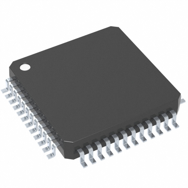
PT PACKAGE
(TOP VIEW)
48 47 46 45 44 43 42 41 40 39 38 37
OUTPUT VCC-4
OUTPUT-4
BOOT CAP.L-4
BOOT CAP.H-4
OUTPUT BIAS -4
NONINV INPUT-4
INV INPUT-4
FEEDBACK-4
NONINV INPUT-3
INV INPUT-3
FEEDBACK-3
VCC
1
36
2
35
3
34
4
33
5
32
6
31
7
30
8
29
9
28
10
27
11
26
12
25
2
SCP
VREF
GND
STANDBY-4
STANDBY-3
STANDBY-2
STANDBY
FEEDBACK-2
INV INPUT-2
NONINV INPUT-2
RT
CT
13 14 15 16 17 18 19 20 21 22 23 24
POST OFFICE BOX 655303
• DALLAS, TEXAS 75265
OUTPUT VCC–1
OUTPUT-1
BOOT CAP.L-1
BOOT CAP.H-1
OUTPUT BIAS-1
DTC-1
OUTPUT MONITOR-1
NONINV INPUT-1
INV INPUT-1
FEEDBACK-1
DTC-2
OUTPUT MONITOR-2
�TL1464I
QUAD PULSE-WIDTH-MODULATION CONTROL CIRCUIT
SLVS266 – FEBRUARY 2000
functional block diagram
BC_H1
BC_L1
OUTVCC1
DCT1
++
OUT1
BIAS1
–
SCP
GND12
+
–
OM1
COMP1
ERR AMP1
–
+
FB1
INV1
NON1
BC_H2
BC_L2
OUTVCC1
DCT2
++
OUT2
BIAS2
–
SCP
+
–
OM2
COMP2
ERR AMP2
–
+
FB2
INV2
NON2
BC_H3
BC_L3
OUTVCC3
ERR AMP3
–
+
COMP3
+
FB3
INV3
NON3
OUT3
BIAS3
–
SCP
+
–
GND34
BC_H4
BC_L4
OUTVCC4
ERR AMP4
–
+
COMP4
+
FB4
INV4
NON4
OUT4
BIAS4
–
SCP
+
–
Standby
Logic
CT
OSC
RT
+
SCP
Standby
Logic
VREF
STANDBY
Voltage
REF
– SCP
Comp
GND
U.V.L.O.
VCC
STANDBY3
STANDBY1 STANDBY2
POST OFFICE BOX 655303
• DALLAS, TEXAS 75265
3
�TL1464I
QUAD PULSE-WIDTH-MODULATION CONTROL CIRCUIT
SLVS266 – FEBRUARY 2000
Terminal Functions
TERMINAL
NAME
NO.
I/O
DESCRIPTION
BOOT CAP.H-1
33
BOOT CAP.L-1
34
BOOT CAP.H-2
39
BOOT CAP.L-2
40
BOOT CAP.H-3
46
BOOT CAP.L-3
45
BOOT CAP.H-4
4
BOOT CAP.L-4
3
CT
14
Timing capacitor connect pin
DTC-1
31
Dead-time control input pin (CH-1)
DTC-2
26
Dead-time control input pin (CH-2)
FEEDBACK-1
27
Error amplifier output pin (CH-1)
FEEDBACK-2
22
Error amplifier output pin (CH-2)
FEEDBACK-3
11
Error amplifier output pin (CH-3)
FEEDBACK-4
8
Error amplifier output pin (CH-4)
GND
17
Ground pin
INV INPUT-1
28
Error amplifier inverting input pin (CH-1)
INV INPUT-2
23
Error amplifier inverting input pin (CH-2)
INV INPUT-3
10
Error amplifier inverting input pin (CH-3)
INV INPUT-4
7
Error amplifier inverting input pin (CH-4)
NONINV INPUT-1
29
Error amplifier noninverting input pin (CH-1)
NONINV INPUT-2
24
Error amplifier noninverting input pin (CH-2)
NONINV INPUT-3
9
Error amplifier noninverting input pin (CH-3)
NONINV INPUT-4
6
Error amplifier noninverting input pin (CH-4)
OUTPUT-1
35
Output pin (CH-1)
OUTPUT-2
41
Output pin (CH-2)
OUTPUT-3
44
Output pin (CH-3)
OUTPUT-4
2
Output pin (CH-4)
OUTPUT BIAS-1
32
Output ON current setup pin (CH-1)
OUTPUT BIAS-2
38
Output ON current setup pin (CH-2)
OUTPUT BIAS-3
47
Output ON current setup pin (CH-3)
OUTPUT BIAS-4
5
Output ON current setup pin (CH-4)
OUTPUT GND-1,2
37
Output ground pin (CH-1,2)
OUTPUT GND-3,4
48
Output ground pin (CH-3,4)
OUTPUT MONITOR-1
30
Output monitor comparator input pin (CH-1)
OUTPUT MONITOR-2
25
Output monitor comparator input pin (CH-2)
OUTPUT VCC-1
36
Output supply pin (CH-1)
OUTPUT VCC-2
42
Output supply pin (CH-2)
OUTPUT VCC-3
43
Output supply pin (CH-3)
OUTPUT VCC-4
1
Output supply pin (CH-4)
RT
SCP
13
Timing resistor connect pin
15
Short-circuit protection capacitor connect pin
4
Boot strap capacitor connect pin (CH
Boot-strap
(CH-1)
1)
Boot strap capacitor connect pin (CH
Boot-strap
(CH-2)
2)
Boot strap capacitor connect pin (CH
Boot-strap
(CH-3)
3)
Boot strap capacitor connect pin (CH
4)
Boot-strap
(CH-4)
POST OFFICE BOX 655303
• DALLAS, TEXAS 75265
�TL1464I
QUAD PULSE-WIDTH-MODULATION CONTROL CIRCUIT
SLVS266 – FEBRUARY 2000
Terminal Functions (Continued)
TERMINAL
NAME
NO.
I/O
DESCRIPTION
STANDBY
21
Output-1 to 4 control pin. Input L level voltage (0.4 V max). All outputs function and VREF are shutdown.
STANDBY-2
20
Output-2 control pin. Input L level voltage (0.4 V max), output-2 function is shutdown.
STANDBY-3
19
Output-3 control pin. Input L level voltage (0.4 V max), output-3 function is shutdown.
STANDBY-4
18
Output-4 control pin. Input L level voltage (0.4 V max), output-4 function is shutdown.
VCC
12
Power supply pin
absolute maximum ratings over operating free-air temperature (unless otherwise noted)†
Supply voltage range, VCC (see Note 1) . . . . . . . . . . . . . . . . . . . . . . . . . . . . . . . . . . . . . . . . . . . . . . . . . . . . . . 13 V
Amplifier input voltage, VIC . . . . . . . . . . . . . . . . . . . . . . . . . . . . . . . . . . . . . . . . . . . . . . . . . . . . . . . . . . . . . . . . . . 13 V
Output voltage, VO . . . . . . . . . . . . . . . . . . . . . . . . . . . . . . . . . . . . . . . . . . . . . . . . . . . . . . . . . . . . . . . . . . . . . . . . . 13 V
Peak output current (sink), I(SINK) . . . . . . . . . . . . . . . . . . . . . . . . . . . . . . . . . . . . . . . . . . . . . . . . . . . . . . . . . 100 mA
Peak output current (source), ISOURCE . . . . . . . . . . . . . . . . . . . . . . . . . . . . . . . . . . . . . . . . . . . . . . . . . . . . . . . . 1 A
Continuous total dissipation at (or below) 25°C free-air temperature (unit), PD . . . . . . . . . . . . . . . . . . 695 mW
Continuous total dissipation at (or below) 25°C free-air temperature (using board), PD
(see Note 2) . . . . . . . . . . . . . . . . . . . . . . . . . . . . . . . . . . . . . . . . . . . . . . . . . . . . . . . . . . . . . . . . . . . 1315 mW
Operating free-air temperature range, TA . . . . . . . . . . . . . . . . . . . . . . . . . . . . . . . . . . . . . . . . . . . . – 20°C to 75°C
Storage temperature range, Tstg . . . . . . . . . . . . . . . . . . . . . . . . . . . . . . . . . . . . . . . . . . . . . . . . . . . – 65°C to 150°C
Lead temperature 1,6 mm (1/16 inch) from case for 10 seconds . . . . . . . . . . . . . . . . . . . . . . . . . . . . . . . 260°C
† Stresses beyond those listed under “absolute maximum ratings” may cause permanent damage to the device. These are stress ratings only, and
functional operation of the device at these or any other conditions beyond those indicated under “recommended operating conditions” is not
implied. Exposure to absolute-maximum-rated conditions for extended periods may affect device reliability.
NOTES: 1. All voltage4 value are with respect to network ground terminal.
2. Using t1.6 × 50 × 50 mm glass epoxy resin.
recommended operating conditions
MIN
Supply voltage, VCC
Amplifier input voltage,
voltage VIC
Standby input voltage,
voltage VI (pins 18
18, 19
19. 20
20. 21)
NOM
MAX
UNIT
3.1
12
V
CH-1,2
–0.1
CH-3,4
0
VCC–1.8
VCC–1.8
V
H level
2.4
VCC
0.4
V
L level
Output voltage, VO
Current into feedback terminal, I(CAMP)
Feedback resistor, R(NF)
100
Boot-strap capacitor, C(BOOT)
100
Bias resistor, R(BIAS)
1.2
Bias capacitor, C(BIAS)
Timing capacitor, C(T)
V
µA
kΩ
500
pF
20
30
Timing resistor, R(T)
12
–45
200
pF
7
50
kΩ
68
1000
Oscillation frequency, f(OSC)
0.05
2
MHz
Operating free-air temperature, TA
–20
75
°C
POST OFFICE BOX 655303
• DALLAS, TEXAS 75265
pF
5
�TL1464I
QUAD PULSE-WIDTH-MODULATION CONTROL CIRCUIT
SLVS266 – FEBRUARY 2000
electrical characteristics over recommended operating free-air temperature range, VCC = 6 V, f =
1 MHz (unless otherwise noted)
reference section
PARAMETER
TEST CONDITIONS
Vref
R(EGIN)
Output voltage (pin 16)
TA = 25°C,
VOS = 3.1 V to 12 V,
R(EFL)
Output regulation
V(RTC1)
R(RTC2)
Output voltage change with temperature
IOS
Short-circuit output current
Input regulation
I(OR) = –1 mA
I(OR) = –1 mA
MIN
TYP
MAX
1.485
1.50
1.515
V
2
12.5
mV
1
7.5
mV
–0.2%
±2%
–0.2%
±2%
I(OR) = –0.1 mA to –1 mA
TA = 20°C to 25°C
TA = 25°C to 75°C
Vref = 0 V
4
8
MIN
TYP
UNIT
mA
undervoltage lockout section
PARAMETER
TEST CONDITIONS
MAX
UNIT
VIH
VIL
Upper threshold voltage
2.7
V
Lower threshold voltage
2.5
V
Vhys
VR
Hysteresis
0.1
0.2
V
2.2
2.3
V
MIN
TYP
TA = 25°C
Reset threshold voltage (VCC)
output voltage monitor section
PARAMETER
TEST CONDITIONS
VIO(M)
Input offset voltage
TA = 25°C (CH-1,2)
VI = 1.5 V (pins 6 and 9),
TA = 25°C (CH-3,4)
I(BOM)
Input bias current
VI = 0 V
V(IOM)
Input voltage range
UNIT
V
10.5
–200
VCC = 3.1 V ~ 12 V
MAX
0
–500
0 to
VCC–1.8
nA
V
protection control section
PARAMETER
V(tPC)
V(stby)
Input threshold voltage (pin 15)
VI
I(bPC)
Latched input voltage (pin 15)
TEST CONDITIONS
TA = 25°C
Standby voltage (pin 15)
Input source current (pin 15)
TA = 25°C
MIN
TYP
MAX
1.45
1.50
1.55
V
40
70
100
mV
10
30
mV
–3
–6
µA
TYP
MAX
–1
UNIT
oscillator section
PARAMETER
TEST CONDITIONS
Frequency
Ct = 100 pF,
Standard deviation of frequency
All values are constant
7%
f(dV)
f(dT1)
Frequency change with voltage
VCC = 3 V ~ 12 V
TA = 20°C to 25°C
1%
–0.5%
±4%
TA = 25°C to 75°C
0.5%
±4%
f(dT2)
6
Frequency change with temperature
POST OFFICE BOX 655303
• DALLAS, TEXAS 75265
Rt = 10 kΩ
MIN
f(OSC)
f(dev)
1
UNIT
MHz
�TL1464I
QUAD PULSE-WIDTH-MODULATION CONTROL CIRCUIT
SLVS266 – FEBRUARY 2000
electrical characteristics over recommended operating free-air temperature range, VCC = 6 V, f =
1 MHz (unless otherwise noted) (continued)
dead-time control section
PARAMETER
I(Idt)
I(dt)
Input current
V(dt)
VIO
Latched input voltage
TEST CONDITIONS
Latched mode sink current
Input
In
ut threshold voltage
V(tt00)
MIN
TYP
MAX
UNIT
–1
–4
µA
1
2
mA
TA = 25°C
I(dt) = 100 µA
0.3
Zero duty cycle
0.6
0.7
0.8
100% duty cycle
1.3
1.4
1.5
MIN
TYP
MAX
UNIT
0.5
V
V
error-amplifier section
PARAMETER
TEST CONDITIONS
VIO
IIO
Input offset voltage
Input offset current
VO = 1 V
VO = 1 V
IIB
Input bias current
VO = 1 V
–200
CH-1,2
VICR
Common mode input voltage
Common-mode
VCC = 3.1
3 1 V ~ 12 V
CH-3,4
A(v)
B1
Open-loop voltage amplification
CMRR
Common-mode rejection ratio
Maximum output voltage swing
IO(vr+)
Output current (sink)
II+
Sink current (pin 24) (standby mode)
IOM–
Output current (source)
mV
nA
–500
nA
–0.1 to
VCC–1.8
V
0 to
VCC–1.8
RI = 200 kΩ
60
75
dB
6
MHz
VIC = –0.1 V ~ VCC – 1.8 V
60
80
dB
Unity-gain bandwidth
VOM+
VOM–
±10
±100
Vref–0.1
0.2
V
VID = –0.1 V, VO = 1.25 V
VI = 0.3 V (pin 24)
VI = 0 V (pin 20)
0.5
1
mA
0.1
0.5
mA
VID = 0.1 V,
–45
–85
µA
VO = 0.75 V
output section
PARAMETER
I(SINK)
Output current (sink)
MIN
TYP
MAX
R(BIAS) = 2.4 kΩ
TEST CONDITIONS
15
20
25
R(BIAS) = 5.8 kΩ
7.5
10
12.5
MIN
TYP
MAX
UNIT
mA
total device
PARAMETER
IO(CS)
IO(CA)
TEST CONDITIONS
UNIT
Standby supply current
Standby pin input voltage = 0 V
1
200
µA
Average supply current
Rt = 10 kΩ
4
7
mA
POST OFFICE BOX 655303
• DALLAS, TEXAS 75265
7
�TL1464I
QUAD PULSE-WIDTH-MODULATION CONTROL CIRCUIT
SLVS266 – FEBRUARY 2000
OSCILLATOR
WAVEFORM (see Note A)
1.4 V
DEAD-TIME
INPUT VOLTAGE
ERROR AMP. OUTPUT
0.7 V
0V
“H”
PWM COMP. OUTPUT
“L”
DEAD-TIME 100%
“H”
OUTPUT PIN WAVEFORM
“L”
REGULATED OUTPUT
VOLTAGE (see Note B)
VA
VA
VA
0V
Vref + 0.7 V
1.5 V
SCP PIN WAVEFORM
tpe
“H”
SCP COMP. OUTPUT
“L”
POWER SUPPLY
VOLTAGE
VCC
2.7 V
0V
Protection Enable Time, tpe = 477×103 Cpe (sec)
Figure 1. Timing Diagram (CH-1/CH-2)
OSCILLATOR
WAVEFORM (see Note A)
ERROR AMP. OUTPUT
1.4 V
0.7 V
“H”
PWM COMP. OUTPUT
“L”
DEAD-TIME 100%
“H”
OUTPUT PIN WAVEFORM
“L”
REGULATED OUTPUT
VOLTAGE (see Note B)
VA
VA
VA
0V
Vref + 0.7 V
1.5 V
SCP PIN WAVEFORM
tpe
“H”
SCP COMP. OUTPUT
“L”
POWER SUPPLY
VOLTAGE
VCC
2.7 V
0V
Protection Enable Time, tpe = 477×103 Cpe (sec)
Figure 2. Timing Diagram (CH-3/CH-4)
NOTES: A. Oscillator waveform of CH-1 and CH-2 is inverting output each other.
B. Va = input voltage of pin 29 (pin 24)
8
POST OFFICE BOX 655303
• DALLAS, TEXAS 75265
�TL1464I
QUAD PULSE-WIDTH-MODULATION CONTROL CIRCUIT
SLVS266 – FEBRUARY 2000
MECHANICAL DATA
PT (S-PQFP-G48)
PLASTIC QUAD FLATPACK
0,27
0,17
0,50
36
0,08 M
25
37
24
48
13
0,13 NOM
1
12
5,50 TYP
7,20
SQ
6,80
9,20
SQ
8,80
Gage Plane
0,25
0,05 MIN
1,45
1,35
Seating Plane
1,60 MAX
0°– 7°
0,75
0,45
0,10
4040052 / C 11/96
NOTES: A.
B.
C.
D.
All linear dimensions are in millimeters.
This drawing is subject to change without notice.
Falls within JEDEC MS-026
This may also be a thermally enhanced plastic package with leads conected to the die pads.
POST OFFICE BOX 655303
• DALLAS, TEXAS 75265
9
�PACKAGE OPTION ADDENDUM
www.ti.com
10-Dec-2020
PACKAGING INFORMATION
Orderable Device
Status
(1)
Package Type Package Pins Package
Drawing
Qty
Eco Plan
(2)
Lead finish/
Ball material
MSL Peak Temp
Op Temp (°C)
Device Marking
(3)
(4/5)
(6)
TL1464IPT
ACTIVE
LQFP
PT
48
250
RoHS & Green
NIPDAU
Level-1-260C-UNLIM
-20 to 75
Z1464
(1)
The marketing status values are defined as follows:
ACTIVE: Product device recommended for new designs.
LIFEBUY: TI has announced that the device will be discontinued, and a lifetime-buy period is in effect.
NRND: Not recommended for new designs. Device is in production to support existing customers, but TI does not recommend using this part in a new design.
PREVIEW: Device has been announced but is not in production. Samples may or may not be available.
OBSOLETE: TI has discontinued the production of the device.
(2)
RoHS: TI defines "RoHS" to mean semiconductor products that are compliant with the current EU RoHS requirements for all 10 RoHS substances, including the requirement that RoHS substance
do not exceed 0.1% by weight in homogeneous materials. Where designed to be soldered at high temperatures, "RoHS" products are suitable for use in specified lead-free processes. TI may
reference these types of products as "Pb-Free".
RoHS Exempt: TI defines "RoHS Exempt" to mean products that contain lead but are compliant with EU RoHS pursuant to a specific EU RoHS exemption.
Green: TI defines "Green" to mean the content of Chlorine (Cl) and Bromine (Br) based flame retardants meet JS709B low halogen requirements of


 工商网监
湘ICP备2023018690号
工商网监
湘ICP备2023018690号
