TL16C2552
www.ti.com
SLWS163A – SEPTEMBER 2005 – REVISED JUNE 2006
1.8-V to 5-V DUAL UART WITH 16-BYTE FIFOS
FEATURES
•
•
•
•
•
•
•
•
•
•
•
•
•
•
•
•
•
Programmable Auto-RTS and Auto-CTS
In Auto-CTS Mode, CTS Controls the
Transmitter
In Auto-RTS Mode, RCV FIFO Contents, and
Threshold Control RTS
Serial and Modem Control Outputs Drive a
RJ11 Cable Directly When Equipment is on
the Same Power Drop
Capable of Running With All Existing
TL16C450 Software
After Reset, All Registers Are Identical to the
TL16C450 Register Set
Up to 24-MHz Clock Rate for up to 1.5-Mbaud
Operation With VCC = 5 V
Up to 20-MHz Clock Rate for up to
1.25-Mbaud Operation With VCC = 3.3 V
Up to 16-MHz Clock Rate for up to 1-Mbaud
Operation With VCC = 2.5 V
Up to 10-MHz Clock Rate for up to 625-kbaud
Operation With VCC = 1.8 V
In the TL16C450 Mode, Hold and Shift
Registers Eliminate the Need for Precise
Synchronization Between the CPU and Serial
Data
Programmable Baud Rate Generator Allows
Division of Any Input Reference Clock by 1 to
(216 - 1) and Generates an Internal 16 × Clock
Standard Asynchronous Communication Bits
(Start, Stop, and Parity) Added to or Deleted
From the Serial Data Stream
5-V, 3.3-V, 2.5-V, and 1.8 V Operation
Independent Receiver Clock Input
Transmit, Receive, Line Status, and Data Set
Interrupts Independently Controlled
Fully Programmable Serial Interface
Characteristics:
– 5-, 6-, 7-, or 8-Bit Characters
– Even-, Odd-, or No-Parity Bit Generation
and Detection
– 1-, 1 ½-, or 2-Stop Bit Generation
– Baud Generation (dc to 1 Mbit/s)
•
•
•
•
•
•
•
•
•
•
False-Start Bit Detection
Complete Status Reporting Capabilities
3-State Output TTL Drive Capabilities for
Bidirectional Data Bus and Control Bus
Line Break Generation and Detection
Internal Diagnostic Capabilities:
– Loopback Controls for Communications
Link Fault Isolation
– Break, Parity, Overrun, and Framing Error
Simulation
Fully Prioritized Interrupt System Controls
Modem Control Functions (CTS, RTS, DSR,
DTR, RI, and DCD)
Available in 44-Pin PLCC (FN) or 32-Pin QFN
(RHB) Packages
Each UART's Internal Register Set May Be
Written Concurrently to Save Setup Time
Multi-Function Output (MF) Allows Users to
Select Among Several Functions, Saving
Package Pins
APPLICATIONS
•
•
•
•
•
•
Point-of-Sale Terminals
Gaming Terminals
Portable Applications
Router Control
Cellular Data
Factory Automation
DESCRIPTION
The TL16C2552 is a dual universal asynchronous
receiver and transmitter (UART). It incorporates the
functionality of two TL16C550D UARTs, each UART
having its own register set and FIFOs. The two
UARTs share only the data bus interface and clock
source, otherwise they operate independently.
Another name for the UART function is
Asynchronous Communications Element (ACE), and
these terms will be used interchangeably. The bulk
of this document describes the behavior of each
ACE, with the understanding that two such devices
are incorporated into the TL16C2552.
Please be aware that an important notice concerning availability, standard warranty, and use in critical applications of Texas
Instruments semiconductor products and disclaimers thereto appears at the end of this data sheet.
PRODUCTION DATA information is current as of publication date.
Products conform to specifications per the terms of the Texas
Instruments standard warranty. Production processing does not
necessarily include testing of all parameters.
Copyright © 2005–2006, Texas Instruments Incorporated
�TL16C2552
www.ti.com
SLWS163A – SEPTEMBER 2005 – REVISED JUNE 2006
CTSA
CDA
1 44 43 42 41 40
DSRA
2
RIA
3
VCC
D0
TXRDYA
4
D1
D2
D4
5
D5
7
39
RXA
8
38
TXA
D7
9
37
DTRA
A0
10
36
RTSA
XTAL1
11
35
MFA
GND
12
34
INTA
XTAL2
13
33
VCC
A1
14
32
TXRDYB
A2
15
31
RIB
CHSEL
16
30
CDB
INTB
17
29
DSRB
TL16C2552FN
CTSB
DTRB
TXB
IOR
RXB
RTSB
GND
IOW
RESET
CS
MFB
18 19 20 21 22 23 24 25 26 27 28
D5
D4
D3
D2
D1
D0
VCC
CTSA
32
31
30
29
28
27
26
25
RHB PACKAGE
(TOP VIEW)
D6
1
24
RXA
D7
2
23
TXA
A0
3
22
RTSA
XTAL1
4
21
INTA
XTAL2
5
20
GND
A1
6
19
NC
A2
7
18
NC
CHSEL
8
17
CTSB
10
11
12
13
14
15
16
CS
IOW
RESET
RTSB
IOR
RXB
TXB
TL16C2552RHB
9
Each ACE has a TXRDY and RXRDY output that
can be used to interface to a DMA controller.
6
D6
Each ACE performs serial-to-parallel conversions on
data received from a peripheral device or modem
and stores the parallel data in its receive buffer or
FIFO, and each ACE performs parallel-to-serial
conversions on data sent from its CPU after storing
the parallel data in its transmit buffer or FIFO. The
CPU can read the status of either ACE at any time.
Each ACE includes complete modem control
capability and a processor interrupt system that can
be tailored to the application.
Each ACE includes a programmable baud rate
generator capable of dividing a reference clock with
divisors of from 1 to 65535, thus producing a 16×
internal reference clock for the transmitter and
receiver logic. Each ACE accommodates up to a
1.5-Mbaud serial data rate (24-MHz input clock). As
a reference point, that speed would generate a
667-ns bit time and a 6.7-µs character time (for 8,N,1
serial data), with the internal clock running at 24
MHz.
D3
FN PACKAGE
(TOP VIEW)
INTB
Each ACE is a speed and voltage range upgrade of
the TL16C550C, which in turn is a functional
upgrade of the TL16C450. Functionally equivalent to
the TL16C450 on power up or reset (single character
or TL16C450 mode), each ACE can be placed in an
alternate FIFO mode. This relieves the CPU of
excessive software overhead by buffering received
and to be transmitted characters. Each receiver and
transmitter store up to 16 bytes in their respective
FIFOs, with the receive FIFO including three
additional bits per byte for error status. In the FIFO
mode, a selectable autoflow control feature can
significantly reduce software overload and increase
system efficiency by automatically controlling serial
data flow using handshakes between the RTS output
and CTS input, thus eliminating overruns in the
receive FIFO.
NC − No internal connection
NOTE: The 32-pin RHB package does not provide access to DSRA,
DSRB, RIA, RIB, CDA, CDB inputs and MFA, MFB, DTRA, DTRB,
TXRDYA, TXRDYB outputs.
2
Submit Documentation Feedback
�TL16C2552
www.ti.com
SLWS163A – SEPTEMBER 2005 – REVISED JUNE 2006
TL16C2552 Block Diagram
UART Channel A
TXA
A2 − A0
16 Byte Tx FIFO
D7 − D0
Tx
CS
CTSA
DTRA
UART Regs
CHSEL
BAUD
Rate
Gen
IOR
IOW
DSRA, RIA, CDA
RTSA
16 Byte Rx FIFO
Rx
RXA
INTA
Data Bus
Interface
INTB
UART Channel B
TXRDYA
TXB
TXRDYB
16 Byte Tx FIFO
Tx
MFA
CTSB
DTRB
MFB
UART Regs
BAUD
Rate
Gen
RESET
DSRB, RIB, CDB
RTSB
16 Byte Rx FIFO
Rx
Crystal
OSC
Buffer
XTAL1
XTAL2
RXB
VCC
GND
A.
MF output allows selection of OP, BAUDOUT, or RXRDY per channel.
DEVICE INFORMATION
TERMINAL FUNCTIONS
TERMINAL
NAME
I/O
DESCRIPTION
FN NO.
RHB NO.
A0
10
3
I
Address 0 select bit. Internal registers address selection
A1
14
6
I
Address 1 select bit. Internal registers address selection
A2
15
7
I
Address 2 select bit. Internal registers address selection
42, 30
–
I
Carrier detect (active low). These inputs are associated with individual UART channels A and
B. A low on these pins indicates that a carrier has been detected by the modem for that
channel. The state of these inputs is reflected in the modem status register (MSR).
CDA, CDB
CHSEL
16
8
I
Channel select. UART channel A or B is selected by the state of this pin when CS is a logic 0.
A logic 0 on the CHSEL selects the UART channel B while a logic 1 selects UART channel A.
CHSEL could just be an address line from the user CPU such as A3. Bit 0 of the alternate
function register (AFR) can temporarily override CHSEL function, allowing the user to write to
both channel register simultaneously with one write cycle when CS is low. It is especially
useful during the initialization routine.
CS
18
10
I
UART chip select (active low). This pin selects channel A or B in accordance with the state of
the CHSEL pin. This allows data to be transferred between the user CPU and the 2552.
I
Clear to send (active low). These inputs are associated with individual UART channels A and
B. A logic low on the CTS pins indicates the modem or data set is ready to accept transmit
data from the 2552. Status can be tested by reading MSR bit 4. These pins only affect the
transmit and receive operations when auto CTS function is enabled through the enhanced
feature register (EFR) bit 7, for hardware flow control operation.
CTSA,
CTSB
40, 28
25, 17
Submit Documentation Feedback
3
�TL16C2552
www.ti.com
SLWS163A – SEPTEMBER 2005 – REVISED JUNE 2006
DEVICE INFORMATION (continued)
TERMINAL FUNCTIONS (continued)
TERMINAL
NAME
FN NO.
RHB NO.
D0-D4
2-6
27 - 31
D5-D7
7-9
32, 1, 2
DSRA,
DSRB
41, 29
–
DTRA,
DTRB
37, 27
–
GND
12, 22
20
DESCRIPTION
I/O
Data bus (bidirectional). These pins are the eight bit, 3-state data bus for transferring
information to or from the controlling CPU. D0 is the least significant bit and the first data bit in
a transmit or receive serial data stream.
I
Data set ready (active low). These inputs are associated with individual UART channels A
and B. A logic low on these pins indicates the modem or data set is powered on and is ready
for data exchange with the UART. The state of these inputs is reflected in the modem status
register (MSR).
O
Data terminal ready (active low). These outputs are associated with individual UART channels
A and B. A logic low on these pins indicates that theTLl16C2552 is powered on and ready.
These pins can be controlled through the modem control register. Writing a 1 to MCR bit 0
sets the DTR output to low, enabling the modem. The output of these pins is high after writing
a 0 to MCR bit 0, or after a reset.
Signal and power ground.
34, 17
21, 9
O
Interrupt A and B (active high). These pins provide individual channel interrupts, INT A and B.
INT A and B are enabled when MCR bit 3 is set to a logic 1, interrupt sources are enabled in
the interrupt enable register (IER). Interrupt conditions include: receiver errors, available
receiver buffer data, available transmit buffer space or when a modem status flag is detected.
INTA-B are in the high-impedance state after reset.
IOR
24
14
I
Read input (active low strobe). A high to low transition on IOR will load the contents of an
internal register defined by address bits A0-A2 onto the TL16C2552 data bus (D0-D7) for
access by an external CPU.
IOW
20
11
I
Write input (active low strobe). A low to high transition on IOW will transfer the contents of the
data bus (D0-D7) from the external CPU to an internal register that is defined by address bits
A0-A2 and CSA and CSB
NC
–
18, 19
INTA, INTB
No internal connection
35, 19
–
O
Multi-function output. This output pin can function as the OP, BAUDOUT, or RXRDY pin. One
of these output signal functions can be selected by the user programmable bits 1-2 of the
alternate function register (AFR). These signal functions are described as follows:
1. OP - When OP (active low) is selected, the MF pin is a logic 0 when MCR bit 3 is set to
a logic 1 (see MCR bit 3). MCR bit 3 defaults to a logic 1 condition after a reset or
power-up.
2. BAUDOUT - When BAUDOUT function is selected, the 16× baud rate clock output is
available at this pin.
3. RXRDY - RXRDY (active low) is intended for monitoring DMA data transfers.
If it is not used, leave it unconnected.
RESET
21
12
I
Reset. RESET will reset the internal registers and all the outputs. The UART transmitter
output and the receiver input will be disabled during reset time. See TL16C2552 external
reset conditions for initialization details. RESET is an active-high input.
RIA, RIB
43, 31
–
I
Ring indicator (active low). These inputs are associated with individual UART channels A and
B. A logic low on these pins indicates the modem has received a ringing signal from the
telephone line. A low to high transition on these input pins generates a modem status
interrupt, if enabled. The state of these inputs is reflected in the modem status register (MSR)
MFA, MFB
4
I/O
RTSA,
RTSB
36, 23
22, 13
O
Request to send (active low). These outputs are associated with individual UART channels A
and B. A low on the RTS pin indicates the transmitter has data ready and waiting to send.
Writing a 1 in the modem control register (MCR bit 1) sets these pins to low, indicating data is
available. After a reset, these pins are set to high. These pins only affects the transmit and
receive operation when auto RTS function is enabled through the enhanced feature register
(EFR) bit 6, for hardware flow control operation.
RXA, RXB
39, 25
24, 15
I
Receive data input. These inputs are associated with individual serial channel data to the
2552. During the local loopback mode, these RX input pins are disabled and TX data is
internally connected to the UART RX input internally.
TXA, TXB
38, 26
23, 16
O
Transmit data. These outputs are associated with individual serial transmit channel data from
the 2552. During the local loopback mode, the TX input pin is disabled and TX data is
internally connected to the UART RX input.
TXRDYA,
TXRDYB
1, 32
–
O
Transmit ready (active low). TXRDY A and B go low when there are at least a trigger level
numbers of spaces available. They go high when the TX buffer is full.
VCC
33, 44
26
I
Power supply inputs.
Submit Documentation Feedback
�TL16C2552
www.ti.com
SLWS163A – SEPTEMBER 2005 – REVISED JUNE 2006
DEVICE INFORMATION (continued)
TERMINAL FUNCTIONS (continued)
TERMINAL
NAME
FN NO.
RHB NO.
I/O
DESCRIPTION
XTAL1
11
4
I
Crystal or external clock input. XTAL1 functions as a crystal input or as an external clock
input. A crystal can be connected between XTAL1 and XTAL2 to form an internal oscillator
circuit (see Figure 5). Alternatively, an external clock can be connected to XTAL1 to provide
custom data rates.
XTAL2
13
5
O
Output of the crystal oscillator or buffered clock. See also XTAL1. XTAL2 is used as a crystal
oscillator output or buffered a clock output.
Detailed Description
Autoflow Control (see Figure 1)
Autoflow control is comprised of auto-CTS and auto-RTS. With auto-CTS, the CTS input must be active before
the transmitter FIFO can emit data. With auto-RTS, RTS becomes active when the receiver needs more data
and notifies the sending serial device. When RTS is connected to CTS, data transmission does not occur unless
the receiver FIFO has space for the data; thus, overrun errors are eliminated using ACE1 and ACE2 from a
TLC16C2552 with the autoflow control enabled. If not, overrun errors occur when the transmit data rate exceeds
the receiver FIFO read latency.
ACE1
RCV
FIFO
ACE2
RX
Serial to
Parallel
RTS
Flow
Control
TX
CTS
Parallel
to Serial
XMT
FIFO
Flow
Control
D7 −D0
D7 −D0
XMT
FIFO
TX
Parallel
to Serial
CTS
Flow
Control
RX
RTS
Serial to
Parallel
RCV
FIFO
Flow
Control
Figure 1. Autoflow Control (Auto-RTS and Auto-CTS) Example
Auto-RTS (See Figure 2 and Figure 3)
Auto-RTS data flow control originates in the receiver timing and control block (see functional block diagram) and
is linked to the programmed receiver FIFO trigger level. When the receiver FIFO level reaches a trigger level of
1, 4, or 8 (see Figure 3), RTS is deasserted. With trigger levels of 1, 4, and 8, the sending ACE may send an
additional byte after the trigger level is reached (assuming the sending ACE has another byte to send) because
it may not recognize the deassertion of RTS until after it has begun sending the additional byte. RTS is
automatically reasserted once the RCV FIFO is emptied by reading the receiver buffer register.
When the trigger level is 14 (see Figure 5), RTS is deasserted after the first data bit of the 16th character is
present on the RX line. RTS is reasserted when the RCV FIFO has at least one available byte space.
Submit Documentation Feedback
5
�TL16C2552
www.ti.com
SLWS163A – SEPTEMBER 2005 – REVISED JUNE 2006
Auto-CTS (See Figure 2)
The transmitter circuitry checks CTS before sending the next data byte. When CTS is active, it sends the next
byte. To stop the transmitter from sending the following byte, CTS must be released before the middle of the last
stop bit that is currently being sent (see Figure 2). The auto-CTS function reduces interrupts to the host system.
When flow control is enabled, CTS level changes do not trigger host interrupts because the device automatically
controls its own transmitter. Without auto-CTS, the transmitter sends any data present in the transmit FIFO and
a receiver overrun error may result.
Enabling Autoflow Control and Auto-CTS
Autoflow control is enabled by setting modem control register bits 5 (autoflow enable or AFE) and 1 (RTS) to a
1. Autoflow incorporates both auto-RTS and auto-CTS. When only auto-CTS is desired, bit 1 in the modem
control register should be cleared (this assumes that a control signal is driving CTS).
Auto-CTS and Auto-RTS Functional Timing
Start
SOUT
Bits 0 −7
Start
Stop
Bits 0 −7 Stop
Start
Bits 0 −7 Stop
CTS
Figure 2. CTS Functional Timing Waveforms
SIN
Start
Byte N
Stop
Start
Byte N+1
Start
Stop
Byte
RTS
RD
(RD RBR)
1
2
N
N+1
Figure 3. RTS Functional Timing Waveforms, RCV FIFO Trigger Level = 1, 4, or 8 Bytes
SIN
RTS
Byte 14
Byte 15
Start
Byte 16
Stop
Start
Byte 18 Stop
RTS Released After the
First Data Bit of Byte 16
RD
(RD RBR)
Figure 4. RTS Functional Timing Waveforms, RCV FIFO Trigger Level = 14 Bytes
6
Submit Documentation Feedback
Stop
�TL16C2552
www.ti.com
SLWS163A – SEPTEMBER 2005 – REVISED JUNE 2006
Internal
Data Bus
9−2
D(7−0)
XTAL1
XTAL2
A0
A1
A2
11
13
Data
Bus
Buffer
Crystal
OSC
Buffer
8
S
e
l
e
c
t
Receiver
FIFO
8
Receiver
Shift
Register
Receiver
Buffer
Register
Receiver
Timing and
Control
Line
Control
Register
CHSEL
RESET
IOR
IOW
TXRDYA
MFA
TXRDYB
MFB
RXA, B
36, 23
RTSA, B
10
14
Divisor
Latch (LS)
15
Baud
Generator
Divisor
Latch (MS)
CS
39, 25
18
16
21
24
Transmitter
Timing and
Control
Line
Status
Register
Select
and
Control
Logic
Transmitter
FIFO
Transmitter
Holding
Register
20
1
35
8
Modem
Control
Register
32
S
e
l
e
c
t
8
Transmitter
Shift
Register
Autoflow
Control
(AFE)
38, 26
TXA, B
8
40, 28
19
37, 27
Modem
Status
Register
8
Modem
Control
Logic
41, 29
42, 30
43, 31
34, 17
CTSA, B
DTRA, B
DSRA, b
CDA,B
RIA, B
INTA, B
VCC
GND
33, 44
12, 22
Power
Supply
Interrupt
Enable
Register
Interrupt
Identification
Register
8
Interrupt
Control
Logic
8
FIFO
Control
Register
A.
Pin numbers shown are for 44-pin PLCC FN package.
Figure 5. Functional Block Diagram
Submit Documentation Feedback
7
�TL16C2552
www.ti.com
SLWS163A – SEPTEMBER 2005 – REVISED JUNE 2006
ABSOLUTE MAXIMUM RATINGS (1)
over operating free-air temperature range (unless otherwise noted)
UNIT
Supply voltage range, VCC (2)
-0.5 V to 7 V
Input voltage range at any input, VI
-0.5 V to 7 V
Output voltage range, VO
-0.5 V to 7 V
Operating free-air temperature, TA, TL16C2552
0°C to 70°C
Operating free-air temperature, TA, TL16C2552I
-40°C to 85°C
Storage temperature range, Tstg
-65°C to 150°C
Lead temperature 1,6 mm (1/16 inch) from case for 10 seconds
(1)
(2)
260°C
Stresses beyond those listed under "absolute maximum ratings" may cause permanent damage to the device. These are stress ratings
only, and functional operation of the device at these or any other conditions beyond those indicated under "recommended operating
conditions" is not implied. Exposure to absolute-maximum-rated conditions for extended periods may affect device reliability.
All voltage values are with respect to VSS.
RECOMMENDED OPERATING CONDITIONS
over operating free-air temperature range (unless otherwise noted)
1.8 V ±10%
MIN
NOM
MAX
UNIT
1.62
1.8
1.98
V
0
VCC
V
High-level input voltage
1.4
1.98
V
Low-level input voltage
-0.3
0.4
V
0
VCC
V
High-level output current (all outputs)
0.5
mA
Low-level output current (all outputs)
1
mA
10
MHz
VCC
Supply voltage
VI
Input voltage
VIH
VIL
VO
Output voltage
IOH
IOL
Oscillator/clock speed
2.5 V ±10%
VCC
Supply voltage
VI
Input voltage
VIH
High-level input voltage
VIL
Low-level input voltage
VO
Output voltage
IOH
High-level output current (all outputs)
IOL
Low-level output current (all outputs)
MIN
NOM
MAX
UNIT
2.25
2.5
2.75
V
0
VCC
V
1.8
2.75
V
-0.3
0.6
V
0
VCC
1
Oscillator/clock speed
3.3 V ±10%
NOM
3.3
2
mA
16
MHz
MAX
UNIT
VCC
Supply voltage
3
VI
Input voltage
0
VIH
High-level input voltage
VIL
Low-level input voltage
VO
Output voltage
VCC
V
IOH
High-level output current (all outputs)
1.8
mA
IOL
Low-level output current (all outputs)
3.2
mA
Oscillator/clock speed
20
MHz
MAX
UNIT
VCC
Supply voltage
VI
Input voltage
3.6
V
VCC
V
0.7VCC
V
0.3VCC
0
5 V ±10%
8
MIN
V
mA
MIN
NOM
4.5
5
0
Submit Documentation Feedback
V
5.5
V
VCC
V
�TL16C2552
www.ti.com
SLWS163A – SEPTEMBER 2005 – REVISED JUNE 2006
RECOMMENDED OPERATING CONDITIONS (continued)
over operating free-air temperature range (unless otherwise noted)
5 V ±10%
MIN
VIH
High-level input voltage
All except XTAL1, XTAL2
XTAL1, XTAL2
VIL
Low-level input voltage
VO
Output voltage
IOH
High-level output current (all outputs)
IOL
Low-level output current (all outputs)
NOM
MAX
UNIT
2
V
0.7VCC
All except XTAL1, XTAL2
0.8
XTAL1, XTAL2
V
0.3VCC
0
VCC
V
4
Oscillator/clock speed
mA
4
mA
24
MHz
ELECTRICAL CHARACTERISTICS
over recommended ranges of supply voltage and operating free-air temperature (unless otherwise noted)
1.8 V Nominal
PARAMETER
TEST CONDITIONS
MIN
TYP (1) MAX
UNIT
VOH
High-level output voltage (2)
VOL
Low-level output
voltage (2)
IOL = 1 mA
0.5
V
II
Input current
VCC = 1.98 V, VSS = 0, VI = 0 to 1.98 V, All other terminals
floating
10
µA
IOZ
High-impedance-state output
current
VCC = 1.98 V, VSS = 0, VI = 0 to 1.98 V, Chip selected in write
mode or chip deselected
±20
µA
ICC
Supply current
VCC = 1.98 V, TA = 0°C, RXA, RXB, DSRA, DSRB, CDA, CDB,
CTSA, CTSB, RIA, and RIB at 1.4 V, All other inputs at 0.4 V,
XTAL1 at 10 MHz, No load on outputs
1.5
mA
Ci(CL
Clock input impedance
15
20
pF
20
30
pF
6
10
pF
10
20
pF
IOH = -0.5 mA
1.3
V
K)
CO(C
Clock output impedance
LK)
CI
Input impedance
CO
Output impedance
(1)
(2)
VCC = 0, VSS = 0, f = 1 MHz,
TA = 25°C, All other terminals grounded
All typical values are at VCC = 1.8 V and TA = 25°C.
These parameters apply for all outputs except XTAL2.
ELECTRICAL CHARACTERISTICS
over recommended ranges of supply voltage and operating free-air temperature (unless otherwise noted)
2.5 V Nominal
PARAMETER
TEST CONDITIONS
MIN TYP (1) MAX
UNIT
VOH
High-level output voltage (2)
VOL
Low-level output
voltage (2)
IOL = 2 mA
0.5
V
II
Input current
VCC = 2.75 V, VSS = 0, VI = 0 to 2.75 V, All other terminals
floating
10
µA
IOZ
High-impedance-state output
current
VCC = 2.75 V, VSS = 0, VI = 0 to 2.75 V, Chip selected in
write mode or chip deselected
±20
µA
ICC
Supply current
VCC = 2.75 V, TA = 0°C, RXA, RXB, DSRA, DSRB, CDA,
CDB, CTSA, CTSB, RIA, and RIB at 1.8 V, All other inputs at
0.6 V, XTAL1 at 16 MHz, No load on outputs
2.5
mA
(1)
(2)
IOH = -1 mA
1.8
V
All typical values are at VCC = 2.5 V and TA = 25°C.
These parameters apply for all outputs except XTAL2.
ADDED SPACE
Submit Documentation Feedback
9
�TL16C2552
www.ti.com
SLWS163A – SEPTEMBER 2005 – REVISED JUNE 2006
ELECTRICAL CHARACTERISTICS (continued)
over recommended ranges of supply voltage and operating free-air temperature (unless otherwise noted)
2.5 V Nominal
PARAMETER
TEST CONDITIONS
MIN TYP (1) MAX
UNIT
Ci(CLK)
Clock input impedance
15
20
pF
CO(CLK)
Clock output impedance
20
30
pF
CI
Input impedance
6
10
pF
CO
Output impedance
10
20
pF
VCC = 0, VSS = 0, f = 1 MHz,
TA = 25°C, All other terminals grounded
ELECTRICAL CHARACTERISTICS
over recommended ranges of supply voltage and operating free-air temperature (unless otherwise noted)
3.3 V Nominal
PARAMETER
TEST CONDITIONS
MIN
TYP (1)
MAX
UNIT
VOH
High-level output voltage (2)
VOL
Low-level output
voltage (2)
IOL = 3.2 mA
0.5
V
II
Input current
VCC = 3.6 V, VSS = 0, VI = 0 to 3.6 V, All other terminals
floating
10
µA
IOZ
High-impedance-state output
current
VCC = 3.6 V, VSS = 0, VI = 0 to 3.6 V, Chip selected in
write mode or chip deselected
±20
µA
ICC
Supply current
VCC = 3.6 V, TA = 0°C, RXA, RXB, DSRA, DSRB, CDA,
CDB, CTSA, CTSB, RIA, and RIB at 2 V, All other inputs
at 0.8 V, XTAL1 at 20 MHz, No load on outputs
4
mA
Ci(CLK)
Clock input impedance
15
20
pF
CO(CLK)
Clock output impedance
20
30
pF
CI
Input impedance
6
10
pF
CO
Output impedance
10
20
pF
(1)
(2)
10
IOH = -1.8 mA
VCC = 0, VSS = 0, f = 1 MHz,
TA = 25°C, All other terminals grounded
All typical values are at VCC = 3.3 V and TA = 25°C.
These parameters apply for all outputs except XTAL2.
Submit Documentation Feedback
2.4
V
�TL16C2552
www.ti.com
SLWS163A – SEPTEMBER 2005 – REVISED JUNE 2006
ELECTRICAL CHARACTERISTICS
over recommended ranges of supply voltage and operating free-air temperature (unless otherwise noted)
5 V Nominal
PARAMETER
TEST CONDITIONS
TYP (1)
MIN
MAX
UNIT
VOH
High-level output voltage (2)
VOL
Low-level output
voltage (2)
IOL = 4 mA
0.4
V
II
Input current
VCC = 5.5 V, VSS = 0, VI = 0 to 5.5 V, All other
terminals floating
10
µA
IOZ
High-impedance-state output
current
VCC = 5.5 V, VSS = 0, VI = 0 to 5.5 V, Chip selected in
write mode or chip deselected
±20
µA
ICC
Supply current
VCC = 5.5 V, TA = 0°C, RXA, RXB, DSRA, DSRB,
CDA, CDB, CTSA, CTSB, RIA, and RIB at 2 V, All
other inputs at 0.8 V, XTAL1 at 24 MHz, No load on
outputs
7.5
mA
Ci(CLK)
Clock input impedance
15
20
pF
CO(CLK)
Clock output impedance
20
30
pF
CI
Input impedance
6
10
pF
CO
Output impedance
10
20
pF
(1)
(2)
IOH = -4 mA
4
V
VCC = 0, VSS = 0, f = 1 MHz,
TA = 25°C, All other terminals grounded
All typical values are at VCC = 5 V and TA = 25°C.
These parameters apply for all outputs except XTAL2.
TIMING REQUIREMENTS
over recommended ranges of supply voltage and operating free-air temperature (unless otherwise noted)
LIMITS
PARAMETER
ALT.
SYMBOL
FIGURE
TEST
CONDITIONS
1.8 V
MIN
tw8
Pulse duration, RESET
tw1
Pulse duration, clock high
tRESET
tXH
tw2
Pulse duration, clock low
tXL
tcR
Cycle time, read (tw7 + td8 + th7)
tcW
Cycle time, write (tw6 + td5 + th4)
tw6
Pulse duration, IOW or CS
tw7
2.5 V
MAX
MIN
3.3 V
MAX
MIN
5V
MAX
MIN
UNIT
MAX
1
1
1
1
µs
6
40
25
20
18
ns
RC
8
115
80
62
57
ns
WC
7
115
80
62
57
ns
tIOW
7
80
55
45
40
ns
Pulse duration, IOR or CS
tIOR
8
80
55
45
40
ns
tSU3
Setup time, data valid before IOW↑ or CS↑
tDS
7
25
20
15
15
ns
th4
Hold time, address valid after IOW↑ or CS↑
tWA
7
20
15
10
10
ns
th5
Hold time, data valid after IOW↑ or CS↑
tDH
7
15
10
5
5
ns
th7
Hold time, data valid after IOR↑ or CS↑
tRA
8
20
15
10
10
ns
td5
Delay time, address valid before IOW↓ or CS↓
tAW
7
15
10
7
7
ns
td8
Delay time, address valid to IOR↓ or CS↓
tAR
8
15
10
7
7
td10
Delay time, IOR↓ or CS↓ to data valid
tRVD
8
CL = 30 pF
55
35
25
20
ns
td11
Delay time, IOR↑ or CS↑ to floating data
tHZ
8
CL = 30 pF
40
30
20
20
ns
td12
Write cycle to write cycle delay
7
100
75
60
50
ns
td13
Read cycle to read cycle delay
8
100
75
60
50
ns
ns
BAUD GENERATOR SWITCHING CHARACTERISTICS
over recommended ranges of supply voltage and operating free-air temperature, CL = 30 pF (for FN package only)
LIMITS
PARAMETER
ALT.
SYMBOL
FIGURE
TEST
CONDITIONS
1.8 V
MIN
MAX
2.5 V
MIN
3.3 V
MAX
MIN
5V
MAX
MIN
UNIT
MAX
tw3
Pulse duration, BAUDOUT low
tLW
6
CLK ÷ 2
80
50
42
35
tw4
Pulse duration, BAUDOUT high
tHW
6
CLK ÷ 2
80
50
42
35
td1
Delay time, XIN↑ to BAUDOUT↑
tBLD
6
55
40
30
25
ns
td2
Delay time, XIN↑↓ to BAUDOUT↓
tBHD
6
55
40
30
25
ns
Submit Documentation Feedback
ns
ns
11
�TL16C2552
www.ti.com
SLWS163A – SEPTEMBER 2005 – REVISED JUNE 2006
RECEIVER SWITCHING CHARACTERISTICS
over recommended ranges of supply voltage and operating free-air temperature (unless otherwise noted)
(1)
LIMITS
ALT.
SYMBOL
PARAMETER
TEST
CONDITIONS
FIGURE
1.8 V
MIN
2.5 V
MAX
MIN
3.3 V
MAX
MIN
5V
MAX
td12
Delay time, RCLK to sample
tSCD
9
20
15
10
td13
Delay time, stop to set INT or read RBR to LSI
interrupt or stop to RXRDY↓
tSINT
8, 9, 10,
11, 12
1
1
1
td14
Delay time, read RBR/LSR to reset INT
tRINT
8, 9, 10,
11, 12
CL = 30 pF
100
90
80
td26
Delay time, RCV threshold byte to RTS↑
19
td27
Delay time, read of last byte in receive FIFO to
RTS↓
td28
td29
(1)
(2)
MIN
UNIT
MAX
10
1
ns
RCLK
cycle
70
ns
CL = 30 pF
2
baudout
cycles (2)
19
CL = 30 pF
2
baudout
cycles
Delay time, first data bit of 16th character to RTS↑
20
CL = 30 pF
2
baudout
cycles
Delay time, RBRRD low to RTS↓
20
CL = 30 pF
2
baudout
cycles
In the FIFO mode, the read cycle (RC) = 1 baudclock (min) between reads of the receive FIFO and the status registers (interrupt
identification register or line status register).
A baudout cycle is equal to the period of the input clock divided by the programmed divider in DLL, DLM.
TRANSMITTER SWITCHING CHARACTERISTICS
over recommended ranges of supply voltage and operating free-air temperature (unless otherwise noted)
LIMITS
PARAMETER
ALT. SYMBOL
FIGURE
TEST
CONDITIONS
1.8 V
2.5 V
3.3 V
5V
UNIT
MIN
MAX
MIN
MAX
MIN
MAX
MIN
MAX
td15
Delay time, initial write to transmit start
tIRS
14
8
24
8
24
8
24
8
24
baudout
cycles
td16
Delay time, start to INT
tSTI
14
8
10
8
10
8
10
8
10
baudout
cycles
td17
Delay time, IOW (WR THR) to reset INT
tHR
14
td18
Delay time, initial write to INT (THRE (1))
tSI
14
td19
Delay time, read IOR↑ to reset INT (THRE (1))
tIR
14
CL = 30 pF
70
50
td20
Delay time, write to TXRDY inactive
tWXI
15, 16
CL = 30 pF
60
45
td21
Delay time, start to TXRDY active
tSXA
15, 16
CL = 30 pF
9
9
tSU4
Setup time, CTS↑ before midpoint of stop bit
18
td25
Delay time, CTS low to TX↓
18
(1)
CL = 30 pF
70
16
34
30
60
16
50
34
16
20
CL = 30 pF
50
ns
34
baudout
cycles
35
35
ns
35
35
ns
9
9
baudout
cycles
24
baudout
cycles
34
10
24
16
10
24
ns
24
THRE = Transmitter Holding Register Empty; IIR = Interrupt Identification Register.
MODEM CONTROL SWITCHING CHARACTERISTICS
over operating free-air temperature range (unless otherwise noted)
LIMITS
PARAMETER
ALT.
SYMBOL
FIGURE
TEST
CONDITIONS
1.8 V
MIN
2.5 V
MAX
MIN
3.3 V
MAX
MIN
5V
MAX
MIN
UNIT
MAX
td22
Delay time, WR MCR to output
tMDO
17
CL = 30 pF
90
70
60
50
ns
td23
Delay time, modem interrupt to set INT
tSIM
17
CL = 30 pF
60
50
40
35
ns
td24
Delay time, RD MSR to reset INT
tRIM
17
CL = 30 pF
80
60
50
40
ns
12
Submit Documentation Feedback
�TL16C2552
www.ti.com
SLWS163A – SEPTEMBER 2005 – REVISED JUNE 2006
Typical Characteristics
Supply Current
vs
Frequency
Supply Current
vs
Frequency
0.5
VCC = 2.5 V
TA = 22°C
1.0
Divisor = 1
0.9
Divisor = 2
0.3
Divisor = 3
Divisor = 10
Divisor = 255
0.2
ICC − Supply Current − mA
0.4
ICC − Supply Current − mA
Divisor = 1
1.1
VCC = 1.8 V
TA = 22°C
0.1
Divisor = 2
0.8
Divisor = 3
0.7
Divisor = 10
Divisor = 255
0.6
0.5
0.4
0.3
0.2
0.1
0.0
0
1
2
3
4
5
6
7
8
9
0.0
10
0
2
4
f − Frequency − MHz
10
12
14
16
G002
Figure 7.
Supply Current
vs
Frequency
Supply Current
vs
Frequency
4.0
Divisor = 1
VCC = 3.3 V
TA = 22°C
Divisor = 1
VCC = 5 V
TA = 22°C
3.6
1.6
3.2
Divisor = 2
1.4
Divisor = 3
1.2
Divisor = 10
Divisor = 255
1.0
0.8
0.6
ICC − Supply Current − mA
ICC − Supply Current − mA
8
Figure 6.
2.0
1.8
6
f − Frequency − MHz
G001
Divisor = 3
2.4
1.6
1.2
0.8
0.2
0.4
0
2
4
6
8
10
12
14
16
18
20
Divisor = 10
Divisor = 255
2.0
0.4
0.0
Divisor = 2
2.8
0.0
0
f − Frequency − MHz
G003
Figure 8.
4
8
12
16
20
24
f − Frequency − MHz
G004
Figure 9.
Submit Documentation Feedback
13
�TL16C2552
www.ti.com
SLWS163A – SEPTEMBER 2005 – REVISED JUNE 2006
N
tw1
tw2
XTAL
td2
td1
MFA,B
(1/1)
td1
td2
MFA,B
(1/2)
tw3
tw4
MFA,B
(1/3)
MFA,B
(1/N)
(N > 3)
2 XIN Cycles
(N −2) XIN Cycles
Figure 10. Input Clock and Baud Generator Timing Waveforms
(For FN Package Only) (When AFR2:1 = 01)
CHSEL,
A2 −A0
Valid Address
Valid Address
td5
td5
th4
th4
tw6
tw6
CS
td12
tw6
tw6
IOW
tsu3
D7 −D0
th5
Valid Data
Figure 11. Write Cycle Timing Waveforms
14
Submit Documentation Feedback
tsu3
th5
Valid Data
�TL16C2552
www.ti.com
SLWS163A – SEPTEMBER 2005 – REVISED JUNE 2006
CHSEL,
A2 −A0
Valid Address
Valid Address
td8
td8
th7
th7
tw7
tw7
CS
td13
tw7
tw7
IOR
td10
td10
td11
D7 −D0
th11
Valid Data
Valid Data
Figure 12. Read Cycle Timing Waveforms
RCLK
(Internal)
td12
8 CLKs
Sample Clock
(Internal)
TL16C450 Mode:
RXA, RXB
Start
Data Bits 5− 8
Parity
Stop
Sample Clock
INT
(data ready)
50%
td13
INT
(RCV error)
td14
50%
50%
IOR
(read RBR)
IOR
(read LSR)
50%
50%
50%
Active
Active
td14
Figure 13. Receiver Timing Waveforms
Submit Documentation Feedback
15
�TL16C2552
www.ti.com
SLWS163A – SEPTEMBER 2005 – REVISED JUNE 2006
RXA, RXB
Data Bits 5 −8
Stop
Sample Clock
(Internal)
Trigger Level
INT
(FCR6, 7 = 0, 0)
50%
50%
(FIFO at or above
trigger level)
(FIFO below
trigger level)
td13
(see Note A)
INT
Line Status
Interrupt (LSI)
td14
50%
50%
td14
IOR
(RD LSR)
Active
50%
Active
IOR
(RD RBR)
50%
Figure 14. Receive FIFO First Byte (Sets DR Bit) Waveforms
RXA, RXB
Stop
Sample Clock
(Internal)
Time-Out or
Trigger Level
Interrupt
50%
50%
(FIFO below
trigger level)
td13
td14
(see Note A)
50%
Line Status
Interrupt (LSI)
td13
50%
Top Byte of FIFO
td14
IOP
(RD LSR)
IOR
(RD RBR)
(FIFO at or above
trigger level)
50%
50%
Active
50%
Active
Previous Byte
Read From FIFO
Figure 15. Receive FIFO Bytes Other Than the First Byte (DR Internal Bit Already Set) Waveforms
16
Submit Documentation Feedback
�TL16C2552
www.ti.com
SLWS163A – SEPTEMBER 2005 – REVISED JUNE 2006
IOR
(RD RBR)
50%
Active
See Note A
RXA, RXB
(first byte)
Stop
Sample Clock
(Internal)
td13
(see Note B)
td14
50%
50%
RXRDYA, RXRDYB
Figure 16. Receiver Ready (RXRDY) Waveforms, FCR0 = 0 or FCR0 = 1 and FCR3 = 0 (Mode 0)
IOR
(RD RBR)
Active
50%
See Note A
RXA, RXB
(first byte that reaches
the trigger level)
Sample Clock
(Internal)
td13
(see Note B)
td14
50%
RXRDYA, RXRDYB
50%
Figure 17. Receiver Ready (RXRDY) Waveforms, FCR0 = 1 and FCR3 = 1 (Mode 1)
Start
50%
TXA, TXB
Data Bits
Parity
td15
INT
(THRE)
50%
Stop
Start
50%
td16
50%
50%
50%
50%
td18
td17
td17
IOW 50%
(WR THR)
50%
50%
td19
IOR
50%
Figure 18. Transmitter Timing Waveforms
Submit Documentation Feedback
17
�TL16C2552
www.ti.com
SLWS163A – SEPTEMBER 2005 – REVISED JUNE 2006
Byte 1
IOW
(WR THR)
TXA, TXB
50%
Data
Parity
Stop
Start
50%
td21
td20
TXRDYA, TXRDYB
50%
50%
Figure 19. Transmitter Ready (TXRDY) Waveforms, FCR0 = 0 or FCR0 = 1 and FCR3 = 0 (Mode 0)
Byte 16
IOW
(WR THR)
TXA, TXB
50%
Data
Parity
Stop
td21
td20
TXRDYA, TXRDYB
Start
50%
50%
50%
FIFO Full
Figure 20. Transmitter Ready (TXRDY) Waveforms, FCR0 = 1 and FCR3 = 1 (Mode 1)
IOW
(WR MCR)
50%
50%
td22
td22
RTSA, RTSB, DTRA,
DTRB, OPA, OPB
50%
50%
50%
CTSA, CTSB, DSRA,
DSRB, CDA, CDB
td23
INT
(modem)
50%
50%
50%
td24
IOR
(RD MSR)
td23
50%
RI
50%
Figure 21. Modem Control Timing Waveforms
18
Submit Documentation Feedback
�TL16C2552
www.ti.com
SLWS163A – SEPTEMBER 2005 – REVISED JUNE 2006
tsu4
CTSA, CTSB
50%
50%
td25
TXA, TXB
50%
Midpoint of Stop Bit
Figure 22. CTS and TX Autoflow Control Timing (Start and Stop) Waveforms
Midpoint of Stop Bit
RXA, RXB
td26
td27
50%
50%
RTSA,
RTSB
50%
IOR
Figure 23. Auto-RTS Timing for RCV Threshold of 1, 4, or 8 Waveforms
Midpoint of Data Bit 0
RXA,
RXB
15th Character
16th Character
td28
td29
50%
50%
RTSA,
RTSB
50%
IOR
Figure 24. Auto-RTS Timing for RCV Threshold of 14 Waveforms
Submit Documentation Feedback
19
�TL16C2552
www.ti.com
SLWS163A – SEPTEMBER 2005 – REVISED JUNE 2006
APPLICATION INFORMATION
TXA, B
D7 −D0
D7 −D0
MEMR or I/OR
MEMW or I/OW
INTR
C
P
U
B
u
s
RESET
A0
A1
A2
RXA, B
IOR
RTSA, B
IOW
DTRA, B
INTA, B
DSRA, B
RESET
EIA-232-D
Drivers
and Receivers
CDA, B
A0
CTSA, B
A1
RIA, B
A2
TL16C2552
A3
CHSEL
XTAL1
CS
CS
3.072 MHz
33 pF
XTAL2
(Optional)
33 pF
Figure 25. Basic TL16C2552 Configuration
20
Submit Documentation Feedback
�TL16C2552
www.ti.com
SLWS163A – SEPTEMBER 2005 – REVISED JUNE 2006
APPLICATION INFORMATION (continued)
Alternate
Crystal Control
TL16C2552
XTAL1
11
33 pF
10, 14, 15
A0 −A23
A0 −A2
XTAL2
13
(Optional)
16
Address
Decoder
18
33 pF
CHSEL
CS
CPU
DTRA, B
RTSA, B
37, 27
36, 23
1
21
RSI/ABT
RESET
D0 −D7
2−9
Buffer
(Optional)
AD0−AD15
D0 −D7
43, 31
RIA, B
42, 30
PHI1
20
CDA, B
PHI2
8
41, 29
6
DSRA, B
CTSA, B
PHI1
RSTO
RD
PHI2
24
TCU
20
WR
IOR
40, 28
38, 26
TXA, B
2
IOW
39, 25
RXA, B
34, 17
5
3
INTA, B
7
1
GND
(VSS)
A.
12, 22
33, 44
EIA-232-D
Connector
VCC
Pin numbers shown are for 44-pin PLCC FN package.
Figure 26. Typical TL16C2552 Connection
Submit Documentation Feedback
21
�TL16C2552
www.ti.com
SLWS163A – SEPTEMBER 2005 – REVISED JUNE 2006
PRINCIPLES OF OPERATION
Register Selection
Table 1. Register Selection
DLAB (1)
A2
A1
0
L
L
L
Receiver buffer (read), transmitter holding register (write)
0
L
L
H
Interrupt enable register
0
L
H
L
Interrupt identification register (read only)
(1)
A0
REGISTER
0
L
H
L
FIFO control register (write)
X
L
H
H
Line control register
X
H
L
L
Modem control register
X
H
L
H
Line status register
X
H
H
L
Modem status register
X
H
H
H
Scratch register
1
L
L
L
Divisor latch (LSB)
1
L
L
H
Divisor latch (MSB)
1
L
H
L
Alternate function register (AFR)
The divisor latch access bit (DLAB) is the most significant bit of the line control register. The DLAB signal is controlled by writing to this
bit location (see Table 4).
Table 2. ACE Reset Functions
REGISTER/SIGNAL
RESET CONTROL
RESET STATE
Interrupt enable register
Master reset
All bits cleared (0 - 3 forced and 4 - 7 permanent)
Interrupt identification register
Master reset
Bit 0 is set, bits 1, 2, 3, 6, and 7 are cleared, and bits
4 - 5 are permanently cleared
FIFO control register
Master reset
All bits cleared
Line control register
Master reset
All bits cleared
Modem control register
Master reset
All bits, except bit 3, cleared (6 - 7 permanent), MCR
3 set
Line status register
Master reset
Bits 5 and 6 are set; all other bits are cleared
Modem status register
Master reset
Bits 0 - 3 are cleared; bits 4 - 7 are input signals
TX
Master reset
High
INT
Master reset MCR3
Interrupt condition (receiver error flag)
Interrupt condition (received data available)
Interrupt condition (transmitter holding register
empty)
Interrupt condition (modem status changes)
Output buffer enabled
Read LSR/MR
Low
Read RBR/MR
Low
Read IR/write THR/MR
Low
Read MSR/MR
Low
OP
Master reset
Low
RTS
Master reset
High
DTR
Master reset
High
Scratch register
Master reset
No effect
Divisor latch (LSB and MSB) registers
Master reset
No effect
Receiver buffer register
Master reset
No effect
Master reset
No effect
Transmitter holding register
RCVR FIFO
MR/FCR1 - FCR0/DFCR0
All bits cleared
XMIT FIFO
MR/FCR2 - FCR0/DFCR0
All bits cleared
Master reset
All bits cleared
Alternate function register (AFR)
22
Submit Documentation Feedback
�TL16C2552
www.ti.com
SLWS163A – SEPTEMBER 2005 – REVISED JUNE 2006
Accessible Registers
The system programmer, using the CPU, has access to and control over any of the ACE registers that are
summarized in Table 2. These registers control ACE operations, receive data, and transmit data. Descriptions of
these registers follow Table 3.
Table 3. Summary of Accessible Registers
BIT
NO.
REGISTER ADDRESS
DLAB = 0
DLAB = 1
0
0
1
2
2
3
4
5
6
7
0
1
2
Receiver
Buffer
Register
(Read
Only)
Transmitte
r Holding
Register
(Write
Only)
Interrupt
Enable
Register
Interrupt
Ident
.Register
(Read
Only)
FIFO
Control
Register
(Write
Only)
Line
Control
Register
Modem
Control
Register
Line
Status
Register
Modem
Status
Register
Scratch
Register
Divisor
Latch
(LSB)
Divisor
Latch
(MSB)
Alternate
Function
Register
RBR
THR
IER
IIR
FCR
LCR
MCR
LSR
MSR
SCR
DLL
DLM
AFR
0
Data Bit
0 (1)
Data Bit 0
Enable
Received
Data
Available
Interrupt
(ERBI)
0 if
Interrupt
Pending
FIFO
Enable
Word
Length
Select Bit 0
(WLS0)
Data
Terminal
Ready
(DTR)
Data
Ready
(DR)
Delta Clear
to Send
(∆CTS)
Bit 0
Bit 0
Bit 8
Concurrent
Write
1
Data Bit 1
Data Bit 1
Enable
Transmitter
Holding
Register
Empty
Interrupt
(ETBEI)
Interrupt ID
Bit 1
Receiver
FIFO
Reset
Word
Length
Select Bit 1
(WLS1)
Request to
Send
(RTS)
Overrun
Error (OE)
Delta Data
Set Ready
(∆DSR)
Bit 1
Bit 1
Bit 9
BAUDOUT
Select
2
Data Bit 2
Data Bit 2
Enable
Receiver
Line Status
Interrupt
(ELSI)
Interrupt ID
Bit 2
Transmitter
FIFO
Reset
Number of
Stop Bits
(STB)
OUT1
Parity Error
(PE)
Trailing
Edge Ring
Indicator
(TERI)
Bit 2
Bit 2
Bit 10
RXRDY
Select
3
Data Bit 3
Data Bit 3
Enable
Modem
Status
Interrupt
(EDSSI)
Interrupt ID
Bit 3 (2)
DMA Mode
Select
Parity
Enable
(PEN)
INT
Enable, OP
Control
Framing
Error (FE)
Delta Data
Carrier
Detect
(∆DCD)
Bit 3
Bit 3
Bit 11
0
4
Data Bit 4
Data Bit 4
0
0
Reserved
Even Parity
Select
(EPS)
Loop
Break
Interrupt
(BI)
Clear to
Send
(CTS)
Bit 4
Bit 4
Bit 12
0
5
Data Bit 5
Data Bit 5
0
0
Reserved
Stick Parity
Autoflow
Control
Enable
(AFE)
Transmitter
Holding
Register
(THRE)
Data Set
Ready
(DSR)
Bit 5
Bit 5
Bit 13
0
6
Data Bit 6
Data Bit 6
0
FIFOs
Enabled (2)
Receiver
Trigger
(LSB)
Break
Control
0
Transmitter
Empty
(TEMT)
Ring
Indicator
(RI)
Bit 6
Bit 6
Bit 14
0
7
Data Bit 7
Data Bit 7
0
FIFOs
Enabled (2)
Receiver
Trigger
(MSB)
Divisor
Latch
Access Bit
(DLAB)
0
Error in
RCVR
FIFO (2)
Data
Carrier
Detect
(DCD)
Bit 7
Bit 7
Bit 15
0
(1)
(2)
Bit 0 is the least significant bit. It is the first bit serially transmitted or received.
These bits are always 0 in the TL16C450 mode.
FIFO Control Register (FCR)
The FCR is a write-only register at the same location as the IIR, which is a read-only register. The FCR enables
and clears the FIFOs, sets the receiver FIFO trigger level, and selects the type of DMA signaling.
• Bit 0: This bit, when set, enables the transmitter and receiver FIFOs. Bit 0 must be set when other FCR bits
are written to or they are not programmed. Changing this bit clears the FIFOs.
• Bit 1: This bit, when set, clears all bytes in the receiver FIFO and clears its counter. The shift register is not
cleared. The 1 that is written to this bit position is self-clearing.
• Bit 2: This bit, when set, clears all bytes in the transmit FIFO and clears its counter. The shift register is not
cleared. The 1 that is written to this bit position is self-clearing.
• Bit 3: When FCR0 is set, setting FCR3 causes RXRDY and TXRDY to change from level 0 to level 1.
• Bits 4 and 5: These two bits are reserved for future use.
• Bits 6 and 7: These two bits set the trigger level for the receiver FIFO interrupt (see Table 4).
Submit Documentation Feedback
23
�TL16C2552
www.ti.com
SLWS163A – SEPTEMBER 2005 – REVISED JUNE 2006
Table 4. Receiver FIFO Trigger Level
BIT 7
BIT 6
RECEIVER FIFO TRIGGER LEVEL (BYTES)
0
0
01
0
1
04
1
0
08
1
1
14
FIFO Interrupt Mode Operation
When the receiver FIFO and receiver interrupts are enabled (FCR0 = 1, IER0 = 1, IER2 = 1), a receiver interrupt
occurs as follows:
1. The received data available interrupt is issued to the microprocessor when the FIFO has reached its
programmed trigger level. It is cleared when the FIFO drops below its programmed trigger level.
2. The IIR receive data available indication also occurs when the FIFO trigger level is reached, and like the
interrupt, it is cleared when the FIFO drops below the trigger level.
3. The receiver line status interrupt (IIR = 06) has higher priority than the received data available (IIR = 04)
interrupt.
4. The data ready bit (LSR0) is set when a character is transferred from the shift register to the receiver FIFO.
It is cleared when the FIFO is empty.
When the receiver FIFO and receiver interrupts are enabled:
1. FIFO time-out interrupt occurs if the following conditions exist:
a. At least one character is in the FIFO.
b. The most recent serial character was received more than four continuous character times ago (if two
stop bits are programmed, the second one is included in this time delay).
c. The most recent microprocessor read of the FIFO has occurred more than four continuous character
times before. This causes a maximum character received command to interrupt an issued delay of
160 ms at a 300-baud rate with a 12-bit character.
2. Character times are calculated by using the RCLK input for a clock signal (makes the delay proportional to
the baud rate).
3. When a time-out interrupt has occurred, it is cleared and the timer is cleared when the microprocessor reads
one character from the receiver FIFO.
4. When a time-out interrupt has not occurred, the time-out timer is cleared after a new character is received or
after the microprocessor reads the receiver FIFO.
When the transmitter FIFO and THRE interrupt are enabled (FCR0 = 1, IER1 = 1), transmit interrupts occur as
follows:
1. The transmitter holding register empty interrupt [IIR (3 -0) = 2] occurs when the transmit FIFO is empty. It is
cleared [IIR (3 -0) = 1] when the THR is written to (1 to 16 characters may be written to the transmit FIFO
while servicing this interrupt) or the IIR is read.
2. The transmitter holding register empty interrupt is delayed one character time minus the last stop bit time
when there have not been at least two bytes in the transmitter FIFO at the same time since the last time that
the FIFO was empty. The first transmitter interrupt after changing FCR0 is immediate if it is enabled.
FIFO Polled Mode Operation
With FCR0 = 1 (transmitter and receiver FIFOs enabled), clearing IER0, IER1, IER2, IER3, or all four to 0 puts
the ACE in the FIFO polled mode of operation. Because the receiver and transmitter are controlled separately,
either one or both can be in the polled mode of operation.
In this mode, the user program checks receiver and transmitter status using the LSR. As stated previously:
• LSR0 is set as long as one byte is in the receiver FIFO.
• LSR1 - LSR 4 specify which error(s) have occurred. Character error status is handled the same way as
when in the interrupt mode; the IIR is not affected since IER2 = 0.
• LSR5 indicates when the THR is empty.
• LSR6 indicates that both the THR and TSR are empty.
24
Submit Documentation Feedback
�TL16C2552
www.ti.com
SLWS163A – SEPTEMBER 2005 – REVISED JUNE 2006
•
LSR7 indicates whether any errors are in the receiver FIFO.
There is no trigger level reached or time-out condition indicated in the FIFO polled mode. However, the
receiver and transmitter FIFOs are still fully capable of holding characters.
Interrupt Enable Register (IER)
The IER enables each of the five types of interrupts (see Table 5) and enables INTRPT in response to an
interrupt generation. The IER can also disable the interrupt system by clearing bits 0 through 3. The contents of
this register are summarized in Table 3 and are described in the following bullets.
• Bit 0: When set, this bit enables the received data available interrupt.
• Bit 1: When set, this bit enables the THRE interrupt.
• Bit 2: When set, this bit enables the receiver line status interrupt.
• Bit 3: When set, this bit enables the modem status interrupt.
• Bits 4 through 7: These bits are not used (always cleared).
Interrupt Identification Register (IIR)
The ACE has an on-chip interrupt generation and prioritization capability that permits a flexible interface with the
most popular microprocessors.
The ACE provides four prioritized levels of interrupts:
• Priority 1 - Receiver line status (highest priority)
• Priority 2 - Receiver data ready or receiver character time-out
• Priority 3 - Transmitter holding register empty
• Priority 4 - Modem status (lowest priority)
When an interrupt is generated, the IIR indicates that an interrupt is pending and encodes the type of interrupt in
its three least significant bits (bits 0, 1, and 2). The contents of this register are summarized in Table 3 and
described in Table 5. Details on each bit is as follows:
• Bit 0: This bit is used either in a hardwired prioritized or polled interrupt system. When bit 0 is cleared, an
interrupt is pending. If bit 0 is set, no interrupt is pending.
• Bits 1 and 2: These two bits identify the highest priority interrupt pending as indicated in Table 3.
• Bit 3: This bit is always cleared in TL16C450 mode. In FIFO mode, bit 3 is set with bit 2 to indicate that a
time-out interrupt is pending.
• Bits 4 and 5: These two bits are not used (always cleared).
• Bits 6 and 7: These bits are always cleared in TL16C450 mode. They are set when bit 0 of the FIFO control
register is set.
Table 5. Interrupt Control Functions
INTERRUPT IDENTIFICATION
REGISTER
PRIORITY
LEVEL
BIT 3
BIT 2
BIT 1
BIT 0
0
0
0
1
None
0
1
1
0
0
1
0
1
1
0
INTERRUPT TYPE
INTERRUPT SOURCE
INTERRUPT RESET
METHOD
None
None
None
1
Receiver line status
Overrun error, parity
error, framing error, or
break interrupt
Read the line status
register
0
2
Received data available
Receiver data available in Read the receiver buffer
the TL16C450 mode or
register
trigger level reached in
the FIFO mode
0
2
Character time-out
indication
No characters have been
removed from or input to
the receiver FIFO during
the last four character
times, and there is at
least one character in it
during this time
Submit Documentation Feedback
Read the receiver buffer
register
25
�TL16C2552
www.ti.com
SLWS163A – SEPTEMBER 2005 – REVISED JUNE 2006
Table 5. Interrupt Control Functions (continued)
INTERRUPT IDENTIFICATION
REGISTER
PRIORITY
LEVEL
INTERRUPT TYPE
INTERRUPT SOURCE
INTERRUPT RESET
METHOD
BIT 3
BIT 2
BIT 1
BIT 0
0
0
1
0
3
Transmitter holding
register empty
Transmitter holding
register empty
Read the interrupt
identification register (if
source of interrupt) or
writing into the transmitter
holding register
0
0
0
0
4
Modem status
Clear to send, data set
ready, ring indicator, or
data carrier detect
Read the modem status
register
Line Control Register (LCR)
The system programmer controls the format of the asynchronous data communication exchange through the
LCR. In addition, the programmer is able to retrieve, inspect, and modify the contents of the LCR; this eliminates
the need for separate storage of the line characteristics in system memory. The contents of this register are
summarized in Table 3 and described in the following bulleted list.
• Bits 0 and 1: These two bits specify the number of bits in each transmitted or received serial character.
These bits are encoded as shown in Table 6.
Table 6. Serial Character Word Length
•
BIT 1
BIT 0
WORD LENGTH
0
0
5 bits
0
1
6 bits
1
0
7 bits
1
1
8 bits
Bit 2: This bit specifies either one, one and one-half, or two stop bits in each transmitted character. When bit
2 is cleared, one stop bit is generated in the data. When bit 2 is set, the number of stop bits generated is
dependent on the word length selected with bits 0 and 1. The receiver clocks only the first stop bit
regardless of the number of stop bits selected. The number of stop bits generated in relation to word length
and bit 2 are shown in Table 7.
Table 7. Number of Stop Bits Generated
•
•
•
•
26
BIT 2
Word Length Selected by Bits 1 and 2
Number of Stop Bits Generated
0
Any word length
1
1
5 bits
1½
1
6 bits
2
1
7 bits
2
1
8 bits
2
Bit 3: This bit is the parity enable bit. When bit 3 is set, a parity bit is generated in transmitted data between
the last data word bit and the first stop bit. In received data, if bit 3 is set, parity is checked. When bit 3 is
cleared, no parity is generated or checked.
Bit 4: This bit is the even parity select bit. When parity is enabled (bit 3 is set) and bit 4 is set, even parity
(an even number of logic 1s in the data and parity bits) is selected. When parity is enabled and bit 4 is
cleared, odd parity (an odd number of logic 1s) is selected.
Bit 5: This bit is the stick parity bit. When bits 3, 4, and 5 are set, the parity bit is transmitted and checked as
cleared. When bits 3 and 5 are set and bit 4 is cleared, the parity bit is transmitted and checked as set. If bit
5 is cleared, stick parity is disabled.
Bit 6: This bit is the break control bit. Bit 6 is set to force a break condition; i.e., a condition where TX is
forced to the spacing (cleared) state. When bit 6 is cleared, the break condition is disabled and has no effect
on the transmitter logic; it only effects TX.
Submit Documentation Feedback
�TL16C2552
www.ti.com
SLWS163A – SEPTEMBER 2005 – REVISED JUNE 2006
•
Bit 7: This bit is the divisor latch access bit (DLAB). Bit 7 must be set to access the divisor latches of the
baud generator during a read or write. Bit 7 must be cleared during a read or write to access the receiver
buffer, the THR, or the IER.
Line Status Register (LSR)
NOTE:
The line status register is intended for read operations only; writing to this register is
not recommended outside of a factory testing environment.
The LSR provides information to the CPU concerning the status of data transfers. The contents of this register
are summarized in Table 3 and described in the following bulleted list.
• Bit 0: This bit is the data ready (DR) indicator for the receiver. DR is set whenever a complete incoming
character has been received and transferred into the RBR or the FIFO. DR is cleared by reading all of the
data in the RBR or the FIFO.
NOTE:
Bits 1 through 4 are the error conditions that produce a receiver line status interrupt.
•
•
•
•
•
•
•
Bit 1: This bit is the overrun error (OE) indicator. When OE is set, it indicates that before the character in the
RBR was read, it was overwritten by the next character transferred into the register. OE is cleared every
time the CPU reads the contents of the LSR. If the FIFO mode data continues to fill the FIFO beyond the
trigger level, an overrun error occurs only after the FIFO is full, and the next character has been completely
received in the shift register. An overrun error is indicated to the CPU as soon as it happens. The character
in the shift register is overwritten, but it is not transferred to the FIFO.
Bit 2: This bit is the parity error (PE) indicator. When PE is set, it indicates that the parity of the received
data character does not match the parity selected in the LCR (bit 4). PE is cleared every time the CPU
reads the contents of the LSR. In the FIFO mode, this error is associated with the particular character in the
FIFO to which it applies. This error is revealed to the CPU when its associated character is at the top of the
FIFO.
Bit 3: This bit is the framing error (FE) indicator. When FE is set, it indicates that the received character did
not have a valid (set) stop bit. FE is cleared every time the CPU reads the contents of the LSR. In the FIFO
mode, this error is associated with the particular character in the FIFO to which it applies. This error is
revealed to the CPU when its associated character is at the top of the FIFO. The ACE tries to resynchronize
after a framing error. To accomplish this, it is assumed that the framing error is due to the next start bit. The
ACE samples this start bit twice and then accepts the input data.
Bit 4: This bit is the break interrupt (BI) indicator. When BI is set, it indicates that the received data input was
held low for longer than a full-word transmission time. A full-word transmission time is defined as the total
time to transmit the start, data, parity, and stop bits. BI is cleared every time the CPU reads the contents of
the LSR. In the FIFO mode, this error is associated with the particular character in the FIFO to which it
applies. This error is revealed to the CPU when its associated character is at the top of the FIFO. When a
break occurs, only one 0 character is loaded into the FIFO. The next character transfer is enabled after RX
goes to the marking state for at least two RCLK samples and then receives the next valid start bit.
Bit 5: This bit is the THRE indicator. THRE is set when the THR is empty, indicating that the ACE is ready to
accept a new character. If the THRE interrupt is enabled when THRE is set, an interrupt is generated. THRE
is set when the contents of the THR are transferred to the TSR. THRE is cleared concurrent with the loading
of the THR by the CPU. In the FIFO mode, THRE is set when the transmit FIFO is empty; it is cleared when
at least one byte is written to the transmit FIFO.
Bit 6: This bit is the transmitter empty (TEMT) indicator. TEMT bit is set when the THR and the TSR are
both empty. When either the THR or the TSR contains a data character, TEMT is cleared. In the FIFO
mode, TEMT is set when the transmitter FIFO and shift register are both empty.
Bit 7: In the TL16C450 mode, this bit is always cleared. In the FIFO mode, LSR7 is set when there is at
least one parity, framing, or break error in the FIFO. It is cleared when the microprocessor reads the LSR
and there are no subsequent errors in the FIFO.
Submit Documentation Feedback
27
�TL16C2552
www.ti.com
SLWS163A – SEPTEMBER 2005 – REVISED JUNE 2006
Modem Control Register (MCR)
The MCR is an 8-bit register that controls an interface with a modem, data set, or peripheral device that is
emulating a modem. The contents of this register are summarized in Table 3 and are described in the following
bulleted list.
• Bit 0: This bit (DTR) controls the DTR output.
• Bit 1: This bit (RTS) controls the RTS output.
• Bit 2: This bit (OUT1) is reserved for output and can also be used for loopback mode.
• Bit 3: This bit (OUT2) controls the high-impedance state output buffer for the INT signal and the OP output.
When low, the INT signal is in a high-impedance state and OP is high. When high, the INT signal is enabled
and OP is low. OP is presented on MF when AFR (2:1) = 00.
• Bit 4: This bit (LOOP) provides a local loop back feature for diagnostic testing of the ACE. When LOOP is
set, the following occurs:
– The transmitter TX is set high.
– The receiver RX is disconnected.
– The output of the TSR is looped back into the receiver shift register input.
– The four modem control inputs (CTS, DSR, CD, and RI) are disconnected.
– The four modem control outputs (DTR, RTS, OUT1, and OUT2) are internally connected to the four
modem control inputs.
– The four modem control outputs are forced to the inactive (high) levels.
• Bit 5: This bit (AFE) is the autoflow control enable. When set, the autoflow control as described in the
detailed description is enabled.
In the diagnostic mode, data that is transmitted is immediately received. This allows the processor to verify
the transmit and receive data paths to the ACE. The receiver and transmitter interrupts are fully operational.
The modem control interrupts are also operational, but the modem control interrupt's sources are now the
lower four bits of the MCR instead of the four modem control inputs. All interrupts are still controlled by the
IER.
The ACE flow can be configured by programming bits 1 and 5 of the MCR as shown in Table 8.
Table 8. ACE Flow Configuration
MCR BIT 5 (AFE)
MCR BIT 1 (RTS)
ACE FLOW CONFIGURATION
1
1
Auto-RTS and auto-CTS enabled (autoflow control enabled)
1
0
Auto-CTS only enabled
0
X
Auto-RTS and auto-CTS disabled
Modem Status Register (MSR)
The MSR is an 8-bit register that provides information about the current state of the control lines from the
modem, data set, or peripheral device to the CPU. Additionally, four bits of this register provide change
information; when a control input from the modem changes state, the appropriate bit is set. All four bits are
cleared when the CPU reads the MSR. The contents of this register are summarized in Table 3 and are
described in the following bulleted list.
• Bit 0: This bit is the change in clear-to-send (∆CTS) indicator. ∆CTS indicates that the CTS input has
changed state since the last time it was read by the CPU. When ∆CTS is set (autoflow control is not enabled
and the modem status interrupt is enabled), a modem status interrupt is generated. When autoflow control is
enabled (∆CTS is cleared), no interrupt is generated.
• Bit 1: This bit is the change in data set ready (∆DSR) indicator. ∆DSR indicates that the DSR input has
changed state since the last time it was read by the CPU. When ∆DSR is set and the modem status
interrupt is enabled, a modem status interrupt is generated.
• Bit 2: This bit is the trailing edge of the ring indicator (TERI) detector. TERI indicates that the RI input to the
chip has changed from a low to a high level. When TERI is set and the modem status interrupt is enabled, a
modem status interrupt is generated.
• Bit 3: This bit is the change in data carrier detect (∆DCD) indicator. ∆DCD indicates that the DCD input to
the chip has changed state since the last time it was read by the CPU. When ∆DCD is set and the modem
status interrupt is enabled, a modem status interrupt is generated.
28
Submit Documentation Feedback
�TL16C2552
www.ti.com
SLWS163A – SEPTEMBER 2005 – REVISED JUNE 2006
•
•
•
•
Bit 4: This bit is the complement of the clear-to-send (CTS) input. When the ACE is in the diagnostic test
mode (LOOP [MCR4] = 1), this bit is equal to the MCR bit 1 (RTS).
Bit 5: This bit is the complement of the data set ready (DSR) input. When the ACE is in the diagnostic test
mode (LOOP [MCR4] = 1), this bit is equal to the MCR bit 0 (DTR).
Bit 6: This bit is the complement of the ring indicator (RI) input. When the ACE is in the diagnostic test mode
(LOOP [MCR4] = 1), this bit is equal to the MCR bit 2 (OUT1).
Bit 7: This bit is the complement of the data carrier detect (DCD) input. When the ACE is in the diagnostic
test mode (LOOP [MCR4] = 1), this bit is equal to the MCR bit 3 (OUT2).
Programmable Baud Generator
The ACE contains a programmable baud generator that takes a clock input in the range between dc and 16
MHz and divides it by a divisor in the range between 1 and (216 -1). The output frequency of the baud generator
is sixteen times (16 y) the baud rate. The formula for the divisor is:
divisor = XIN frequency input P (desired baud rate y 16)
Two 8-bit registers, called divisor latches, store the divisor in a 16-bit binary format. These divisor latches must
be loaded during initialization of the ACE in order to ensure desired operation of the baud generator. When
either of the divisor latches is loaded, a 16-bit baud counter is also loaded to prevent long counts on initial load.
Table 9 and Table 10 illustrate the use of the baud generator with crystal frequencies of 1.8432 MHz and 3.072
MHz respectively. For baud rates of 38.4 kbits/s and below, the error obtained is small. The accuracy of the
selected baud rate is dependent on the selected crystal frequency (see Figure 27 for examples of typical clock
circuits).
Table 9. Baud Rates Using a 1.8432-MHz Crystal
DESIRED BAUD
RATE
DIVISOR USED TO GENERATE 16×
CLOCK
50
2304
75
1536
110
1047
0.026
134.5
857
0.058
150
768
300
384
600
192
1200
96
1800
64
2000
58
2400
48
3600
32
4800
24
7200
16
9600
12
19200
6
38400
3
56000
2
PERCENT ERROR DIFFERENCE BETWEEN DESIRED AND
ACTUAL
0.69
2.86
Table 10. Baud Rates Using a 3.072-MHz Crystal
DESIRED BAUD
RATE
DIVISOR USED TO GENERATE 16×
CLOCK
50
3840
75
2560
110
1745
0.026
134.5
1428
0.034
Submit Documentation Feedback
29
�TL16C2552
www.ti.com
SLWS163A – SEPTEMBER 2005 – REVISED JUNE 2006
Table 10. Baud Rates Using a 3.072-MHz Crystal (continued)
DESIRED BAUD
RATE
DIVISOR USED TO GENERATE 16×
CLOCK
150
1280
300
640
600
320
1200
160
1800
107
2000
96
2400
80
3600
53
4800
40
7200
27
9600
20
19200
10
38400
5
0.312
0.628
1.23
VCC
VCC
Driver
XIN
XIN
External
Clock
C1
Crystal
RP
Optional
Driver
Optional
Clock
Output
RX2
Oscillator Clock
to Baud Generator
Logic
XOUT
Oscillator Clock
to Baud Generator
Logic
XOUT
C2
Figure 27. Typical Clock Circuits
Table 11. Typical Crystal Oscillator Network
CRYSTAL
RP
RX2 (optional)
C1
C2
3.072 MHz
1 MΩ
1.5 kΩ
10 - 30 pF
40 - 60 pF
1.8432 MHz
1 MΩ
1.5 kΩ
10 - 30 pF
40 - 60 pF
16 MHz
1 MΩ
0 kΩ
33 pF
33 pF
Receiver Buffer Register (RBR)
The ACE receiver section consists of a receiver shift register (RSR) and a RBR. The RBR is actually a 16-byte
FIFO. Timing is derived from the input clock divided by the programmed devisor. Receiver section control is a
function of the ACE line control register.
The ACE RSR receives serial data from RX. The RSR then concatenates the data and moves it into the RBR
FIFO. In the TL16C450 mode, when a character is placed in the RBR and the received data available interrupt is
enabled (IER0 = 1), an interrupt is generated. This interrupt is cleared when the data is read out of the RBR. In
the FIFO mode, the interrupts are generated based on the control setup in the FIFO control register.
Scratch Register
The scratch register is an 8-bit register that is intended for the programmer's use as a scratchpad in the sense
that it temporarily holds the programmer's data without affecting any other ACE operation.
30
Submit Documentation Feedback
�TL16C2552
www.ti.com
SLWS163A – SEPTEMBER 2005 – REVISED JUNE 2006
Transmitter Holding Register (THR)
The ACE transmitter section consists of a THR and a transmitter shift register (TSR). The THR is actually a
16-byte FIFO. Timing is derived from the input clock divided by the programmed devisor. Transmitter section
control is a function of the ACE line control register.
The ACE THR receives data off the internal data bus and when the shift register is idle, moves it into the TSR.
The TSR serializes the data and outputs it at TX. In the TL16C450 mode, if the THR is empty and the
transmitter holding register empty (THRE) interrupt is enabled (IER1 = 1), an interrupt is generated. This
interrupt is cleared when a character is loaded into the register. In the FIFO mode, the interrupts are generated
based on the control setup in the FIFO control register.
Alternate Function Register (AFR) - Read/Write
This register is used to select specific modes of MF operation and to allow both UART register sets to be written
concurrently.
AFR[0]: Concurrent Write Mode
When this bit is set, the CPU can write concurrently to the same register in both UARTs. This function is
intended to reduce the dual UART initialization time. It can be used by the CPU when both channels are
initialized to the same state. The external CPU can set or clear this bit by accessing either register set. When
this bit is set, the channel select pin still selects the channel to be accessed during read operations. The user
should ensure that LCR bit 7 of both channels are in the same state before executing a concurrent write to the
registers at addresses 0, 1, or 2.
• Logic 0 = No concurrent write (default)
• Logic 1 = Register set A and B are written concurrently with a single external CPU I/O write operation.
AFR[2:1]: MF Output Select
These bits select a signal function for output on the MF A/B pins. These signal functions are described as: OP,
BAUDOUT, or RXRDY. Only one signal function can be selected at a time.
MF Function
Bit 2
Bit 1
MF Function
0
0
OP (default)
0
1
BAUDOUT
1
0
RXRDY
1
1
Reserved
AFR[7:3]: Reserved
All are initialized to logic 0.
Table 12. Typical Package Thermal Resistance Data
Package
32-Pin TQFP RHB
θJA = xx°C/W
θJC = xx°C/W
44-Pin PLCC FN
θJA = 46.2°C/W
θJC = 22°C/W
Table 13. Typical Package Weight
Package
Weight in Grams
32-Pin TQFP RHB
0.15
44-Pin PLCC FN
0.5
Submit Documentation Feedback
31
�PACKAGE MATERIALS INFORMATION
www.ti.com
5-Jan-2022
TUBE
*All dimensions are nominal
Device
Package Name
Package Type
Pins
SPQ
L (mm)
W (mm)
T (µm)
B (mm)
TL16C2552FN
FN
PLCC
44
26
18.42
5.13
640
NA
TL16C2552FNG4
FN
PLCC
44
26
18.42
5.13
640
NA
TL16C2552IFN
FN
PLCC
44
26
18.42
5.13
640
NA
Pack Materials-Page 1
��PACKAGE OUTLINE
FN0044A
PLCC - 4.57 mm max height
SCALE 0.800
PLASTIC CHIP CARRIER
B
.180 MAX
[4.57]
.650-.656
[16.51-16.66]
NOTE 3
A
6
1 44
(.008)
[0.2]
40
7
.020 MIN
[0.51]
39
PIN 1 ID
(OPTIONAL)
.650-.656
[16.51-16.66]
NOTE 3
.582-.638
[14.79-16.20]
17
29
18
28
.090-.120 TYP
[2.29-3.04]
44X .026-.032
[0.66-0.81]
C
SEATING PLANE
44X .013-.021
[0.33-0.53]
.007 [0.18]
C A B
40X .050
[1.27]
.004 [0.1] C
.685-.695
[17.40-17.65]
TYP
4215154/A 04/2017
NOTES:
1. All linear dimensions are in inches. Any dimensions in brackets are in millimeters. Any dimensions in parenthesis are for reference only.
Controlling dimensions are in inches. Dimensioning and tolerancing per ASME Y14.5M.
2. This drawing is subject to change without notice.
3. Dimension does not include mold protrusion. Maximum allowable mold protrusion .01 in [0.25 mm] per side.
4. Reference JEDEC registration MS-018.
www.ti.com
�EXAMPLE BOARD LAYOUT
FN0044A
PLCC - 4.57 mm max height
PLASTIC CHIP CARRIER
SYMM
44X (.093 )
[2.35]
1
6
44
40
7
39
44X (.030 )
[0.75]
SYMM
(.64 )
[16.2]
40X (.050 )
[1.27]
29
17
(R.002 ) TYP
[0.05]
18
28
(.64 )
[16.2]
LAND PATTERN EXAMPLE
EXPOSED METAL SHOWN
SCALE:4X
EXPOSED METAL
.002 MAX
[0.05]
ALL AROUND
METAL
SOLDER MASK
OPENING
.002 MIN
[0.05]
ALL AROUND
EXPOSED METAL
METAL UNDER
SOLDER MASK
SOLDER MASK
OPENING
NON SOLDER MASK
DEFINED
(PREFERRED)
SOLDER MASK
DEFINED
SOLDER MASK DETAILS
4215154/A 04/2017
NOTES: (continued)
5. Publication IPC-7351 may have alternate designs.
6. Solder mask tolerances between and around signal pads can vary based on board fabrication site.
www.ti.com
�EXAMPLE STENCIL DESIGN
FN0044A
PLCC - 4.57 mm max height
PLASTIC CHIP CARRIER
SYMM
44X (.093 )
[2.35]
6
1
44
40
7
39
44X (.030 )
[0.75]
SYMM
(.64 )
[16.2]
40X (.050 )
[1.27]
29
17
(R.002 ) TYP
[0.05]
18
28
(.64 )
[16.2]
SOLDER PASTE EXAMPLE
BASED ON 0.125 mm THICK STENCIL
SCALE:4X
4215154/A 04/2017
NOTES: (continued)
7. Laser cutting apertures with trapezoidal walls and rounded corners may offer better paste release. IPC-7525 may have alternate
design recommendations.
8. Board assembly site may have different recommendations for stencil design.
www.ti.com
�GENERIC PACKAGE VIEW
RHB 32
VQFN - 1 mm max height
PLASTIC QUAD FLATPACK - NO LEAD
5 x 5, 0.5 mm pitch
Images above are just a representation of the package family, actual package may vary.
Refer to the product data sheet for package details.
4224745/A
www.ti.com
�IMPORTANT NOTICE AND DISCLAIMER
TI PROVIDES TECHNICAL AND RELIABILITY DATA (INCLUDING DATA SHEETS), DESIGN RESOURCES (INCLUDING REFERENCE
DESIGNS), APPLICATION OR OTHER DESIGN ADVICE, WEB TOOLS, SAFETY INFORMATION, AND OTHER RESOURCES “AS IS”
AND WITH ALL FAULTS, AND DISCLAIMS ALL WARRANTIES, EXPRESS AND IMPLIED, INCLUDING WITHOUT LIMITATION ANY
IMPLIED WARRANTIES OF MERCHANTABILITY, FITNESS FOR A PARTICULAR PURPOSE OR NON-INFRINGEMENT OF THIRD
PARTY INTELLECTUAL PROPERTY RIGHTS.
These resources are intended for skilled developers designing with TI products. You are solely responsible for (1) selecting the appropriate
TI products for your application, (2) designing, validating and testing your application, and (3) ensuring your application meets applicable
standards, and any other safety, security, regulatory or other requirements.
These resources are subject to change without notice. TI grants you permission to use these resources only for development of an
application that uses the TI products described in the resource. Other reproduction and display of these resources is prohibited. No license
is granted to any other TI intellectual property right or to any third party intellectual property right. TI disclaims responsibility for, and you
will fully indemnify TI and its representatives against, any claims, damages, costs, losses, and liabilities arising out of your use of these
resources.
TI’s products are provided subject to TI’s Terms of Sale or other applicable terms available either on ti.com or provided in conjunction with
such TI products. TI’s provision of these resources does not expand or otherwise alter TI’s applicable warranties or warranty disclaimers for
TI products.
TI objects to and rejects any additional or different terms you may have proposed. IMPORTANT NOTICE
Mailing Address: Texas Instruments, Post Office Box 655303, Dallas, Texas 75265
Copyright © 2022, Texas Instruments Incorporated
�
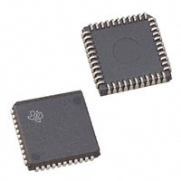


 工商网监
湘ICP备2023018690号
工商网监
湘ICP备2023018690号
