Product
Folder
Sample &
Buy
Support &
Community
Tools &
Software
Technical
Documents
TL1963A, TL1963A-15, TL1963A-18, TL1963A-25, TL1963A-33
SLVS719G – JUNE 2008 – REVISED JANUARY 2015
TL1963A-xx 1.5-A Low-Noise Fast-Transient-Response Low-Dropout Regulator
1 Features
3 Description
•
•
•
•
•
•
•
•
•
The TL1963A-xx devices are low-dropout (LDO)
regulators optimized for fast transient response. The
device can supply 1.5 A of output current with a
dropout voltage of 340 mV. Operating quiescent
current is 1 mA, dropping to less than 1 μA in
shutdown. Quiescent current is well controlled; it does
not rise in dropout as with many other regulators. In
addition to fast transient response, the TL1963A-xx
regulators have very low output noise, which makes
them ideal for sensitive RF supply applications.
1
•
•
•
•
Optimized for Fast Transient Response
Output Current: 1.5 A
Dropout Voltage: 340 mV
Low Noise: 40 μVRMS (10 Hz to 100 kHz)
1-mA Quiescent Current
No Protection Diodes Needed
Controlled Quiescent Current in Dropout
Fixed Output Voltages: 1.5 V, 1.8 V, 2.5 V, 3.3 V
Adjustable Output from 1.21 V to 20 V (TL1963A
Only)
Less Than 1-μA Quiescent Current in Shutdown
Stable With 10-μF Ceramic Output Capacitor
Reverse-Battery Protection
Reverse-Current Protection
Device Information(1)
PART NUMBER
TL1963A
TL1963A-15
Industrial
Wireless Infrastructure
Radio-Frequency Systems
3.3-V to 2.5-V Logic Power Supplies
Post Regulator for Switching Supplies
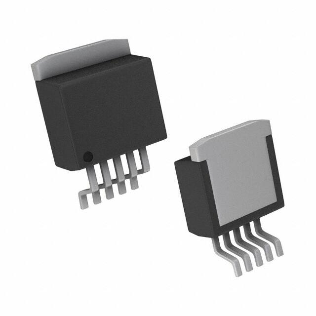
TO-263 (5)
10.16 mm × 8.42 mm
6.50 mm × 3.50 mm
SOT (4)
TO-263 (5)
10.16 mm × 8.42 mm
SOT (6)
TL1963A-18
6.50 mm × 3.50 mm
SOT (4)
TO-263 (5)
10.16 mm × 8.42 mm
SOT (6)
TL1963A-25
6.50 mm × 3.50 mm
SOT (4)
TO-263 (5)
10.16 mm × 8.42 mm
SOT (6)
TL1963A-33
BODY SIZE (NOM)
6.50 mm × 3.50 mm
SOT (6)
2 Applications
•
•
•
•
•
PACKAGE
SOT (6)
6.50 mm × 3.50 mm
SOT (4)
TO-263 (5)
10.16 mm × 8.42 mm
(1) For all available packages, see the orderable addendum at
the end of the data sheet.
Simplified Schematic
Dropout Voltage vs Output Current
500
450
Dropout Voltage – mV
400
350
TA = 125°C
300
250
200
TA = 25°C
150
100
50
0
0
0.2
0.4
0.6
0.8
1
1.2
1.4
1.6
Output Current – A
1
An IMPORTANT NOTICE at the end of this data sheet addresses availability, warranty, changes, use in safety-critical applications,
intellectual property matters and other important disclaimers. PRODUCTION DATA.
�TL1963A, TL1963A-15, TL1963A-18, TL1963A-25, TL1963A-33
SLVS719G – JUNE 2008 – REVISED JANUARY 2015
www.ti.com
Table of Contents
1
2
3
4
5
6
7
8
9
Features ..................................................................
Applications ...........................................................
Description .............................................................
Revision History.....................................................
Description (continued).........................................
Device Comparison Table.....................................
Pin Configuration and Functions .........................
Specifications.........................................................
1
1
1
2
3
3
3
5
8.1
8.2
8.3
8.4
8.5
8.6
5
5
5
5
6
8
Absolute Maximum Ratings .....................................
ESD Ratings..............................................................
Recommended Operating Conditions.......................
Thermal Information ..................................................
Electrical Characteristics...........................................
Typical Characteristics ..............................................
Detailed Description ............................................ 13
9.1 Overview ................................................................. 13
9.2 Functional Block Diagram ....................................... 13
9.3 Feature Description................................................. 13
9.4 Device Functional Modes........................................ 15
10 Application and Implementation........................ 16
10.1 Application Information.......................................... 16
10.2 Typical Applications .............................................. 16
11 Power Supply Recommendations ..................... 21
12 Layout................................................................... 21
12.1 Layout Guidelines ................................................. 21
12.2 Layout Example .................................................... 22
12.3 Thermal Considerations ........................................ 24
13 Device and Documentation Support ................. 26
13.1
13.2
13.3
13.4
Related Links ........................................................
Trademarks ...........................................................
Electrostatic Discharge Caution ............................
Glossary ................................................................
26
26
26
26
14 Mechanical, Packaging, and Orderable
Information ........................................................... 26
4 Revision History
Changes from Revision F (January 2014) to Revision G
•
2
Page
Added ESD Ratings table, Feature Description section, Device Functional Modes, Application and Implementation
section, Power Supply Recommendations section, Layout section, Device and Documentation Support section, and
Mechanical, Packaging, and Orderable Information section ................................................................................................. 1
Submit Documentation Feedback
Copyright © 2008–2015, Texas Instruments Incorporated
Product Folder Links: TL1963A TL1963A-15 TL1963A-18 TL1963A-25 TL1963A-33
�TL1963A, TL1963A-15, TL1963A-18, TL1963A-25, TL1963A-33
www.ti.com
SLVS719G – JUNE 2008 – REVISED JANUARY 2015
5 Description (continued)
Output voltage range is from 1.21 V to 20 V. The TL1963A-xx regulators are stable with output capacitance as
low as 10 μF. Small ceramic capacitors can be used without the necessary addition of ESR as is common with
other regulators. Internal protection circuitry includes reverse-battery protection, current limiting, thermal limiting,
and reverse-current protection. The devices are available in fixed output voltages of 1.5 V, 1.8 V, 2.5 V, 3.3 V,
and as an adjustable device with a 1.21-V reference voltage.
6 Device Comparison Table
DEVICE
OUTPUT VOLTAGE
PIN 5 (DCQ AND KTT ONLY)
TL1963A
Adjustable
ADJ
TL1963A-15
1.5 V
SENSE
TL1963A-18
1.8 V
SENSE
TL1963A-25
2.5 V
SENSE
TL1963A-33
3.3 V
SENSE
7 Pin Configuration and Functions
GND
DCQ PACKAGE
(TOP VIEW)
5
4
3
2
1
6
SENSE/ADJ
OUT
GND
IN
SHDN
GND
DCY PACKAGE
(TOP VIEW)
4
3
OUT
2
GND
1
IN
KTT PACKAGE
(TOP VIEW)
5
4
3
2
1
Copyright © 2008–2015, Texas Instruments Incorporated
SENSE/ADJ
OUT
GND
IN
SHDN
Submit Documentation Feedback
Product Folder Links: TL1963A TL1963A-15 TL1963A-18 TL1963A-25 TL1963A-33
3
�TL1963A, TL1963A-15, TL1963A-18, TL1963A-25, TL1963A-33
SLVS719G – JUNE 2008 – REVISED JANUARY 2015
www.ti.com
Pin Functions
PIN
DESCRIPTION
5
I
Adjust. For the adjustable TL1963A, this is the input to the error amplifier. This pin is clamped
internally to ±7 V. It has a bias current of 3 μA that flows into the pin. The ADJ pin voltage is
1.21 V referenced to ground, and the output voltage range is 1.21 V to 20 V.
3
—
DCQ
DCY
KTT
ADJ
5
—
GND
3, 6
2, 4
Ground
IN
2
1
2
I
Input. Power is supplied to the device through the IN pin. A bypass capacitor is required on
this pin if the device is more than six inches away from the main input filter capacitor. In
general, the output impedance of a battery rises with frequency, so it is advisable to include a
bypass capacitor in battery-powered circuits. A bypass capacitor (ceramic) in the range of
1 μF to 10 μF is sufficient. The TL1963A-xx regulators are designed to withstand reverse
voltages on the IN pin with respect to ground and the OUT pin. In the case of a reverse input,
which can happen if a battery is plugged in backwards, the device acts as if there is a diode in
series with its input. There is no reverse-current flow into the regulator, and no reverse
voltage appears at the load. The device protects both itself and the load.
OUT
4
3
4
O
Output. The output supplies power to the load. A minimum output capacitor (ceramic) of
10 μF is required to prevent oscillations. Larger output capacitors are required for applications
with large transient loads to limit peak voltage transients.
I
Sense. For fixed voltage versions of the TL1963A-xx (TL1963A-1.5, TL1963A-1.8, TL1963A2.5, and TL1963A-3.3), the SENSE pin is the input to the error amplifier. Optimum regulation
is obtained at the point where the SENSE pin is connected to the OUT pin of the regulator. In
critical applications, small voltage drops are caused by the resistance (RP) of PC traces
between the regulator and the load. These may be eliminated by connecting the SENSE pin
to the output at the load as shown in Figure 32. Note that the voltage drop across the external
PCB traces adds to the dropout voltage of the regulator. The SENSE pin bias current is 600
μA at the rated output voltage. The SENSE pin can be pulled below ground (as in a dual
supply system in which the regulator load is returned to a negative supply) and still allow the
device to start and operate.
Shutdown. The SHDN pin is used to put the TL1963A-xx regulators into a low-power
shutdown state. The output is off when the SHDN pin is pulled low. The SHDN pin can be
driven either by 5-V logic or open-collector logic with a pullup resistor. The pullup resistor is
required to supply the pullup current of the open-collector gate, normally several
microamperes, and the SHDN pin current, typically 3 μA. If unused, the SHDN pin must be
connected to VIN. The device is in the low-power shutdown state if the SHDN pin is not
connected.
SENSE
4
I/O
NAME
5
—
5
SHDN
1
—
1
I
Thermal
Pad
—
—
—
—
Submit Documentation Feedback
For the KTT package, the exposed thermal pad is connected to ground and must be soldered
to the PCB for rated thermal performance.
Copyright © 2008–2015, Texas Instruments Incorporated
Product Folder Links: TL1963A TL1963A-15 TL1963A-18 TL1963A-25 TL1963A-33
�TL1963A, TL1963A-15, TL1963A-18, TL1963A-25, TL1963A-33
www.ti.com
SLVS719G – JUNE 2008 – REVISED JANUARY 2015
8 Specifications
8.1 Absolute Maximum Ratings
over operating virtual-junction temperature range (unless otherwise noted)
Input voltage, VIN
(1)
MIN
MAX
IN
–20
20
OUT
–20
20
Input-to-output differential (2)
–20
20
SENSE
–20
20
ADJ
–7
7
SHDN
–20
20
Output short-circuit duration, tshort
UNIT
V
Indefinite
Maximum lead temperature (10-s soldering time), Tlead
300
°C
Maximum junction temperature, TJMAX
125
°C
150
°C
Storage temperature, Tstg
(1)
(2)
–65
Stresses beyond those listed under Absolute Maximum Ratings may cause permanent damage to the device. These are stress ratings
only, and functional operation of the device at these or any other conditions beyond those indicated under Recommended Operating
Conditions is not implied. Exposure to conditions beyond the recommended operating maximum for extended periods may affect device
reliability.
Absolute maximum input-to-output differential voltage cannot be achieved with all combinations of rated IN pin and OUT pin voltages.
With the IN pin at 20 V, the OUT pin may not be pulled below 0 V. The total measured voltage from IN to OUT can not exceed ±20 V.
8.2 ESD Ratings
VALUE
V(ESD)
(1)
(2)
Electrostatic discharge
Human body model (HBM), per ANSI/ESDA/JEDEC JS-001 (1)
±2000
Charged-device model (CDM), per JEDEC specification JESD22C101 (2)
±1000
UNIT
V
JEDEC document JEP155 states that 500-V HBM allows safe manufacturing with a standard ESD control process.
JEDEC document JEP157 states that 250-V CDM allows safe manufacturing with a standard ESD control process.
8.3 Recommended Operating Conditions
over operating free-air temperature range (unless otherwise noted)
VIN
Input voltage range (1)
VIH
SHDN High-Level Input Voltage
VIL
SHDN Low-Level Input Voltage
TJ
Recommended operating junction temperature range
(1)
MIN
MAX
VOUT + VDO
20
V
2
20
V
0.25
V
125
°C
–40
UNIT
TL1963A, TL1963A-15, and TL1963A-18 may require a higher minimum input voltage under some output voltage/load conditions as
indicated under Electrical Characteristics.
8.4 Thermal Information
TL1963A-xx
THERMAL METRIC (1) (2)
KTT
DCQ
DCY
5 PINS
6 PINS
4 PINS
RθJA
Junction-to-ambient thermal resistance
32.9
50.5
57.9
RθJC(top)
Junction-to-case (top) thermal resistance
37.6
31.1
38.6
RθJB
Junction-to-board thermal resistance
18.9
5.1
7.1
ψJT
Junction-to-top characterization parameter
5.7
1.0
1.7
ψJB
Junction-to-board characterization parameter
17.3
5.0
7.0
RθJC(bot)
Junction-to-case (bottom) thermal resistance
1.0
—
—
(1)
(2)
UNIT
°C/W
For more information about traditional and new thermal metrics, see the IC Package Thermal Metrics application report, SPRA953.
For thermal estimates of this device based on PCB copper area, see the TI PCB Thermal Calculator.
Copyright © 2008–2015, Texas Instruments Incorporated
Submit Documentation Feedback
Product Folder Links: TL1963A TL1963A-15 TL1963A-18 TL1963A-25 TL1963A-33
5
�TL1963A, TL1963A-15, TL1963A-18, TL1963A-25, TL1963A-33
SLVS719G – JUNE 2008 – REVISED JANUARY 2015
www.ti.com
8.5 Electrical Characteristics
Over recommended operating temperature range TJ = –40 to 125 °C (unless otherwise noted) (1)
PARAMETER
Minimum input voltage (3) (4)
VIN
TEST CONDITIONS
25°C
1.9
Full range
2.1
2.5
VIN = 2.5 V to 20 V,
ILOAD = 1 mA to 1.5 A
VIN = 2.3 V, ILOAD = 1 mA
TL1963A-18
Regulated output voltage (5)
VIN = 2.8 V to 20 V,
ILOAD = 1 mA to 1.5 A
VIN = 3 V, ILOAD = 1 mA
TL1963A-25
VIN = 3.5 V to 20 V,
ILOAD = 1 mA to 1.5 A
VIN = 3.8 V, ILOAD = 1 mA
TL1963A-33
VIN = 4.3 V to 20 V,
ILOAD = 1 mA to 1.5 A
VIN = 2.21 V, ILOAD = 1 mA
ADJ pin voltage (3) (5)
Line regulation
Load regulation
(1)
(2)
(3)
(4)
(5)
6
MAX
ILOAD = 1.5 A
VIN = 2.21 V, ILOAD = 1 mA
VADJ
MIN TYP (2)
ILOAD = 0.5 A
TL1963A-15
VOUT
TJ
25°C
1.477
1.5
1.523
Full range
1.447
1.5
1.545
25°C
1.773
1.8
1.827
Full range
1.737
1.8
1.854
25°C
2.462
2.5
2.538
Full range
2.412
2.5
2.575
25°C
3.25
3.3
3.35
Full range
3.2
3.3
3.4
25°C
1.192
1.21
1.228
VIN = 2.5 V to 20 V,
ILOAD = 1 mA to 1.5 A
Full range
1.174
1.21
1.246
TL1963A-15
ΔVIN = 2.21 V to 20 V,
ILOAD = 1 mA
Full range
2
6
TL1963A-18
ΔVIN = 2.3 V to 20 V,
ILOAD = 1 mA
Full range
2.5
7
TL1963A-25
ΔVIN = 3 V to 20 V,
ILOAD = 1 mA
Full range
3
10
TL1963A-33
ΔVIN = 3.8 V to 20 V,
ILOAD = 1 mA
Full range
3.5
10
TL1963A (3)
ΔVIN = 2.21 V to 20 V,
ILOAD = 1 mA
Full range
1.5
5
TL1963A-15
VIN = 2.5 V,
ΔILOAD = 1 mA to 1.5 A
Full range
TL1963A-18
VIN = 2.8 V,
ΔILOAD = 1 mA to 1.5 A
Full range
TL1963A
25°C
25°C
25°C
TL1963A-25
VIN = 3.5 V,
ΔILOAD = 1 mA to 1.5 A
Full range
TL1963A-33
VIN = 4.3 V,
ΔILOAD = 1 mA to 1.5 A
Full range
TL1963A (3)
VIN = 2.5 V,
ΔILOAD = 1 mA to 1.5 A
Full range
25°C
25°C
2
UNIT
V
V
V
mV
9
18
2
10
20
2.5
15
30
3
mV
20
70
2
8
18
The TL1963A-xx regulators are tested and specified under pulse load conditions such that TJ ≉ TA. They are fully tested at TA = 25°C.
Performance at –40 and 125°C is specified by design, characterization, and correlation with statistical process controls.
Typical values represent the likely parametric nominal values determined at the time of characterization. Typical values depend on the
application and configuration and may vary over time. Typical values are not ensured on production material.
The TL1963A is tested and specified for these conditions with the ADJ pin connected to the OUT pin.
For the TL1963A, TL1963A-15 and TL1963A-18, dropout voltages are limited by the minimum input voltage specification under some
output voltage/load conditions.
Operating conditions are limited by maximum junction temperature. The regulated output voltage specification does not apply for all
possible combinations of input voltage and output current. When operating at maximum input voltage, the output current range must be
limited. When operating at maximum output current, the input voltage range must be limited.
Submit Documentation Feedback
Copyright © 2008–2015, Texas Instruments Incorporated
Product Folder Links: TL1963A TL1963A-15 TL1963A-18 TL1963A-25 TL1963A-33
�TL1963A, TL1963A-15, TL1963A-18, TL1963A-25, TL1963A-33
www.ti.com
SLVS719G – JUNE 2008 – REVISED JANUARY 2015
Electrical Characteristics (continued)
Over recommended operating temperature range TJ = –40 to 125 °C (unless otherwise noted)(1)
PARAMETER
TEST CONDITIONS
Dropout voltage (4) (6) (7)
VIN = VOUT(NOMINAL)
eN
IADJ
Output voltage noise
ADJ pin bias current
ILOAD = 100 mA
I SHDN
0.1
0.17
0.22
25°C
0.19
Full range
0.27
0.34
Full range
0.45
0.55
ILOAD = 0 mA
Full range
1
1.5
ILOAD = 1 mA
Full range
1.1
1.6
ILOAD = 100 mA
Full range
3.8
5.5
ILOAD = 500 mA
Full range
15
25
ILOAD = 1.5 A
Full range
80
120
25°C
40
25°C
VOUT = OFF to ON
Full range
VOUT = ON to OFF
Full range
0.25
3
10
0.9
2
0.75
25°C
0.01
1
25°C
3
30
Quiescent current in shutdown
VIN = 6 V, V SHDN = 0 V
25°C
0.01
1
Ripple rejection
VIN – VOUT = 1.5 V (avg), VRIPPLE = 0.5 VP-P,
fRIPPLE = 120 Hz, ILOAD = 0.75 A
25°C
VIN = 7 V, VOUT = 0 V
25°C
IIL
Input reverse leakage current
Reverse output current (10)
VIN = VOUT(NOMINAL) + 1
Full range
VIN = –20 V, VOUT = 0 V
Full range
55
mA
μVRMS
V SHDN = 20 V
Current limit
V
0.35
25°C
COUT = 10 μF, ILOAD = 1.5 A,
BW = 10 Hz to 100 kHz
UNIT
0.1
V SHDN = 0 V
SHDN pin current
ILIMIT
IRO
0.06
Full range
(3) (9)
Shutdown threshold
0.02
25°C
ILOAD = 1.5 A
IGND
MAX
Full range
ILOAD = 500 mA
GND pin current (7) (8)
VIN = VOUT(NOMINAL) + 1
MIN TYP (2)
25°C
ILOAD = 1 mA
VDO
TJ
63
μA
V
μA
μA
dB
2
A
1.6
1
TL1963A-15
VOUT = 1.5 V, VIN < 1.5 V
25°C
600
1200
TL1963A-18
VOUT = 1.8 V, VIN < 1.8 V
25°C
600
1200
TL1963A-25
VOUT = 2.5 V, VIN < 2.5 V
25°C
600
1200
TL1963A-33
VOUT = 3.3 V, VIN < 3.3 V
25°C
600
1200
TL1963A
VOUT = 1.21 V, VIN < 1.21 V
25°C
300
600
μA
μA
(6)
Dropout voltage is the minimum input to output voltage differential needed to maintain regulation at a specified output current. In
dropout, the output voltage is equal to: VIN – VDROPOUT.
(7) To satisfy requirements for minimum input voltage, the TL1963A is tested and specified for these conditions with an external resistor
divider (two 4.12-kΩ resistors) for an output voltage of 2.4 V. The external resistor divider adds a 300-µA DC load on the output.
(8) GND pin current is tested with VIN = (VOUT(NOMINAL) + 1 V) and a current source load. The GND pin current decreases at higher input
voltages.
(9) ADJ pin bias current flows into the ADJ pin.
(10) Reverse output current is tested with the IN pin grounded and the OUT pin forced to the rated output voltage. This current flows into the
OUT pin and out the GND pin.
Copyright © 2008–2015, Texas Instruments Incorporated
Submit Documentation Feedback
Product Folder Links: TL1963A TL1963A-15 TL1963A-18 TL1963A-25 TL1963A-33
7
�TL1963A, TL1963A-15, TL1963A-18, TL1963A-25, TL1963A-33
SLVS719G – JUNE 2008 – REVISED JANUARY 2015
www.ti.com
8.6 Typical Characteristics
Typical characteristics apply to all TL1963A-xx devices unless otherwise noted.
480
500
450
IOUT = 1.5 A
400
Dropout Voltage – mV
Dropout Voltage – mV
360
350
TA = 125°C
300
250
200
TA = 25°C
150
240
IOUT = 0.5 A
IOUT = 100 mA
120
100
50
IOUT = 1 mA
0
0
0.2
0.4
0.6
0.8
1
1.2
1.4
0
-50
1.6
-25
0
25
50
75
100
125
TA – Free-Air Temperature – °C
Output Current – A
Figure 1. Dropout Voltage vs Output Current
Figure 2. Dropout Voltage vs Temperature
1.5
VIN = 6 V
1.4
IOUT = 0 A
Quiescent Current – mA
1.3
VSHDN = VIN
1.2
1.1
TL1963A-3.3
VOUT
Fixed 3.3 V
1
0.9
TL1963A
(Adjustable)
VOUT Adjustable
0.8
0.7
0.6
0.5
-50
-25
0
25
50
75
100
125
TA – Free-Air Temperature – °C
VIN = 6 V
IOUT = 0 A
VSHDN = VIN
Figure 3. Quiescent Current vs Temperature
IOUT = 1 mA
TL1963A-25
Figure 5. TL1963A-25 Output Voltage vs Temperature
8
Submit Documentation Feedback
IOUT = 1 mA
TL1963A-18
Figure 4. TL1963A-18 Output Voltage vs Temperature
IOUT = 1 mA
TL1963A-33
Figure 6. TL1963A-33 Output Voltage vs Temperature
Copyright © 2008–2015, Texas Instruments Incorporated
Product Folder Links: TL1963A TL1963A-15 TL1963A-18 TL1963A-25 TL1963A-33
�TL1963A, TL1963A-15, TL1963A-18, TL1963A-25, TL1963A-33
www.ti.com
SLVS719G – JUNE 2008 – REVISED JANUARY 2015
Typical Characteristics (continued)
Typical characteristics apply to all TL1963A-xx devices unless otherwise noted.
1.2
1.23
1.225
Quiescent Current (mA)
1
Output Voltage (V)
1.22
1.215
1.21
1.205
1.2
0.8
0.6
0.4
0.2
1.195
1.19
-50
0
-25
0
25
50
75
Free-Air Temperature (qC)
IOUT = 1 mA
100
0
125
2
D020
TJ = 25 °C
VIN = 6 V
Figure 7. TL1963A Output Voltage vs Temperature
4
6
8
10
12
Input Voltage (V)
14
ROUT = 4.3kΩ
16
18
20
D021
VSHDN = VIN
Figure 8. Quiescent Current vs Input Voltage
10
IOUT = 10 mA
IOUT = 100 mA
IOUT = 300 mA
9
Ground Current (mA)
8
7
6
5
4
3
2
1
0
0
1
2
TJ = 25 °C
3
4
5
6
Input Voltage (V)
7
VOUT = 1.21 V
8
9
10
D022
VSHDN = VIN
Figure 9. TL1963A Ground Current vs Input Voltage
TJ = 25 °C
VSHDN = VIN
Figure 11. TL1963A-33 Ground Current vs Input Voltage
Copyright © 2008–2015, Texas Instruments Incorporated
TJ = 25 °C
VOUT = 1.21 V
VSHDN = VIN
Figure 10. TL1963A Ground Current vs Input Voltage
TJ = 25 °C
VSHDN = VIN
Figure 12. TL1963A-33 Ground Current vs Input Voltage
Submit Documentation Feedback
Product Folder Links: TL1963A TL1963A-15 TL1963A-18 TL1963A-25 TL1963A-33
9
�TL1963A, TL1963A-15, TL1963A-18, TL1963A-25, TL1963A-33
SLVS719G – JUNE 2008 – REVISED JANUARY 2015
www.ti.com
Typical Characteristics (continued)
Typical characteristics apply to all TL1963A-xx devices unless otherwise noted.
VSHDN = 0 V
VIN = VOUT(nom) + 1
Figure 14. Quiescent Current in Shutdown vs Input Voltage
Figure 13. Ground Current vs Output Current
2.5
1
2
0.75
SHDN Input Current – µA
SHDN Input Current (PA)
2.25
0.5
0.25
1.75
1.5
1.25
1
0.75
0.5
0
-50
0.25
-25
0
25
50
75
Free-Air Temperature (qC)
100
125
D011
VSHON = 0 V
0
2
4
6
8
10
12
14
16
18
20
SHDN Input Voltage – V
Figure 15. SHDN Pin Current (ISHDN) vs Temperature
IOUT = 1 mA
Figure 16. SHDN Pin Current (ISHDN) vs SHDN Input Voltage
IOUT = 1 mA
Figure 17. SHDN Threshold (OFF to ON) vs Temperature
10
0
Submit Documentation Feedback
Figure 18. SHDN Threshold (ON to OFF) vs Temperature
Copyright © 2008–2015, Texas Instruments Incorporated
Product Folder Links: TL1963A TL1963A-15 TL1963A-18 TL1963A-25 TL1963A-33
�TL1963A, TL1963A-15, TL1963A-18, TL1963A-25, TL1963A-33
www.ti.com
SLVS719G – JUNE 2008 – REVISED JANUARY 2015
Typical Characteristics (continued)
Typical characteristics apply to all TL1963A-xx devices unless otherwise noted.
5
4.5
ADJ Bias Current – µA
4
3.5
3
2.5
2
1.5
1
0.5
0
-50
-25
0
25
50
75
100
125
TA – Free-Air Temperature – °C
ΔVOUT = 100 mV
Figure 19. ADJ Bias Current vs Temperature
Figure 20. Current Limit vs Input-to-Output Differential
Voltage
12
TJ = 25°C
Reverse Output Current – mA
10
VIN = 0 V
Current flows into OUT pin
8
VOUT(Adjustable)
Adjustable
TL1963A
VOUT =VVOUT
ADJ = VADJ
6
4
2
0
TL1963A-3.3
VOUT
Fixed 3.3 V
V VOUT= =VVFB
OUT
FB
-2
0
2
4
6
8
10
Output Voltage – V
VIN = 7 V
TJ = 25 °C
VIN = 0 V
Current flows into OUT pin
VOUT = 0 V
Figure 21. Current Limit vs Temperature
Figure 22. Reverse Output Current vs Output Voltage
1000
Reverse Output Current – µA
VIN = 0 V
800
600
VOUT
Fixed 3.3V
TL1963A-3.3
VOUT= =3.3
3.3VV
VOUT
400
200
0
-50
V
OUT Adjustable
TL1963A
(Adjustable)
VOUT
OUT =
V
= 1.21
1.21 VV
-25
0
25
50
75
100
125
TA – Free-Air Temperature – °C
VIN = 0 V
Figure 23. Reverse Output Current vs Temperature
Copyright © 2008–2015, Texas Instruments Incorporated
VRIPPLE = 0.05 VPP
VIN = 2.7 V
CIN = 0
TA = 25 °C
COUT = 10 µF (ceramic)
Figure 24. Ripple Rejection vs Frequency
Submit Documentation Feedback
Product Folder Links: TL1963A TL1963A-15 TL1963A-18 TL1963A-25 TL1963A-33
11
�TL1963A, TL1963A-15, TL1963A-18, TL1963A-25, TL1963A-33
SLVS719G – JUNE 2008 – REVISED JANUARY 2015
www.ti.com
Typical Characteristics (continued)
Typical characteristics apply to all TL1963A-xx devices unless otherwise noted.
20
1
IOUT = 1.5 A
15
10(ceramic)
µF
COUTC=OUT
10=µF
IOUT =IOUT
1.5=A1.5 A
TL1963A
VOUT(Adjustable)
Adjustable
5
Output Noise
Hz
Output
NoiseVoltage
Voltage––µV/
µVÖRMS
Load Regulation – mV
10
0
-5
-10
TL1963A-1.8
VOUT
Fixed 1.8 V
-15
TL1963A-2.5
VOUT
Fixed 2.5 V
-20
-25
TL1963A-3.3
V
OUT Fixed 3.3 V
0.1
TL1963A
(Adjustable)
VOUT Adjustable
TL1963A-3.3
VOUT
Fixed 3.3 V
-30
-35
-50
-25
0
25
50
75
100
125
0.01
10
100
TA – Free-Air Temperature – °C
IOUT = 1 mA to 1.5 A
COUT = 10 µF
(ceramic)
Figure 25. Load Regulation vs Temperature
VIN = 4.3 V
CIN = 10 µF
COUT = 10 µF (ceramic)
10k
100k
IOUT = 1.5 A
Figure 26. Output Noise Voltage vs Frequency
VIN = 4.3 V
CIN = 10 µF
COUT = 10 µF (ceramic)
Figure 27. Load Transient Response
IOUT = 1.5 A
1k
Frequency - Hz
Figure 28. Load Transient Response
CIN = 10 µF
COUT = 10 µF (ceramic)
Figure 29. Line Transient response
12
Submit Documentation Feedback
Copyright © 2008–2015, Texas Instruments Incorporated
Product Folder Links: TL1963A TL1963A-15 TL1963A-18 TL1963A-25 TL1963A-33
�TL1963A, TL1963A-15, TL1963A-18, TL1963A-25, TL1963A-33
www.ti.com
SLVS719G – JUNE 2008 – REVISED JANUARY 2015
9 Detailed Description
9.1 Overview
The TL1963A-xx series are 1.5-A low-dropout regulators optimized for fast transient response. The devices can
supply 1.5 A at a dropout voltage of 340 mV. The low operating quiescent current (1 mA) drops to less than 1 μA
in shutdown. In addition to the low quiescent current, the TL1963A-xx regulators incorporate several protection
features that make them ideal for use in battery-powered systems. The devices are protected against both
reverse input and reverse output voltages. In battery-backup applications where the output can be held up by a
backup battery when the input is pulled to ground, the TL1963A-xx acts as if it has a diode in series with its
output and prevents reverse-current flow. Additionally, in dual-supply applications where the regulator load is
returned to a negative supply, the output can be pulled below ground by as much as (20 V – VIN) and still allow
the device to start and operate.
9.2 Functional Block Diagram
9.3 Feature Description
9.3.1 Overload Recovery
Like many IC power regulators, the TL1963A-xx has safe operating area protection. The safe area protection
decreases the current limit as input-to-output voltage increases and keeps the power transistor inside a safe
operating region for all values of input-to-output voltage. The protection is designed to provide some output
current at all values of input-to-output voltage up to the device breakdown.
When power is first turned on, as the input voltage rises, the output follows the input, allowing the regulator to
start up into very heavy loads. During start-up, as the input voltage is rising, the input-to-output voltage
differential is small, allowing the regulator to supply large output currents. With a high input voltage, a problem
can occur wherein removal of an output short does not allow the output voltage to recover. Other regulators also
exhibit this phenomenon, so it is not unique to the TL1963A-xx.
Copyright © 2008–2015, Texas Instruments Incorporated
Submit Documentation Feedback
Product Folder Links: TL1963A TL1963A-15 TL1963A-18 TL1963A-25 TL1963A-33
13
�TL1963A, TL1963A-15, TL1963A-18, TL1963A-25, TL1963A-33
SLVS719G – JUNE 2008 – REVISED JANUARY 2015
www.ti.com
Feature Description (continued)
The problem occurs with a heavy output load when the input voltage is high and the output voltage is low.
Common situations occur immediately after the removal of a short circuit or when the shutdown pin is pulled high
after the input voltage has already been turned on. The load line for such a load may intersect the output current
curve at two points. If this happens, there are two stable output operating points for the regulator. With this
double intersection, the input power supply may need to be cycled down to zero and brought up again to make
the output recover.
9.3.2 Output Voltage Noise
The TL1963A-xx regulators have been designed to provide low output voltage noise over the 10-Hz to 100-kHz
bandwidth while operating at full load. Output voltage noise is typically 35 nV/√Hz over this frequency bandwidth
for the TL1963A (adjustable version). For higher output voltages (generated by using a resistor divider), the
output voltage noise is gained up accordingly. This results in RMS noise over the 10-Hz to 100-kHz bandwidth of
14 μVRMS for the TL1963A, increasing to 38 μVRMS for the TL1963A-33.
Higher values of output voltage noise may be measured when care is not exercised with regard to circuit layout
and testing. Crosstalk from nearby traces can induce unwanted noise onto the output of the TL1963A-xx. Powersupply ripple rejection must also be considered; the TL1963A-xx regulators do not have unlimited power-supply
rejection and pass a small portion of the input noise through to the output.
9.3.3 Protection Features
The TL1963A-xx regulators incorporate several protection features which make them ideal for use in batterypowered circuits. In addition to the normal protection features associated with monolithic regulators, such as
current limiting and thermal limiting, the devices are protected against reverse input voltages, reverse output
voltages and reverse voltages from output to input.
Current limit protection and thermal overload protection are intended to protect the device against current
overload conditions at the output of the device. For normal operation, the junction temperature should not exceed
125°C.
The input of the device withstands reverse voltages of 20 V. Current flow into the device is limited to less than
1 mA (typically less than 100 μA), and no negative voltage appears at the output. The device protects both itself
and the load. This provides protection against batteries that can be plugged in backward.
The output of the TL1963A-xx can be pulled below ground without damaging the device. If the input is left open
circuit or grounded, the output can be pulled below ground by 20 V. For fixed voltage versions, the output acts
like a large resistor, typically 5 kΩ or higher, limiting current flow to typically less than 600 μA. For adjustable
versions, the output acts like an open circuit; no current flows out of the pin. If the input is powered by a voltage
source, the output sources the short-circuit current of the device and protects itself by thermal limiting. In this
case, grounding the SHDN pin turns off the device and stops the output from sourcing the short-circuit current.
The ADJ pin of the adjustable device can be pulled above or below ground by as much as 7 V without damaging
the device. If the input is left open circuit or grounded, the ADJ pin acts like an open circuit when pulled below
ground and like a large resistor (typically 5 kΩ) in series with a diode when pulled above ground.
In situations where the ADJ pin is connected to a resistor divider that would pull the ADJ pin above its 7-V clamp
voltage if the output is pulled high, the ADJ pin input current must be limited to less than 5 mA. For example, a
resistor divider is used to provide a regulated 1.5-V output from the 1.21-V reference when the output is forced to
20 V. The top resistor of the resistor divider must be chosen to limit the current into the ADJ pin to less than
5 mA when the ADJ pin is at 7 V. The 13-V difference between OUT and ADJ divided by the 5-mA maximum
current into the ADJ pin yields a minimum top resistor value of 2.6 kΩ.
In circuits where a backup battery is required, several different input/output conditions can occur. The output
voltage may be held up while the input is either pulled to ground, pulled to some intermediate voltage, or is left
open circuit.
When the IN pin of the TL1963A-xx is forced below the OUT pin or the OUT pin is pulled above the IN pin, input
current typically drops to less than 2 μA. This can happen if the input of the device is connected to a discharged
(low voltage) battery and the output is held up by either a backup battery or a second regulator circuit. The state
of the SHDN pin has no effect on the reverse output current when the output is pulled above the input.
14
Submit Documentation Feedback
Copyright © 2008–2015, Texas Instruments Incorporated
Product Folder Links: TL1963A TL1963A-15 TL1963A-18 TL1963A-25 TL1963A-33
�TL1963A, TL1963A-15, TL1963A-18, TL1963A-25, TL1963A-33
www.ti.com
SLVS719G – JUNE 2008 – REVISED JANUARY 2015
9.4 Device Functional Modes
Table 1. Device States
SHDN
DEVICE STATE
H
Regulated Voltage
L
Shutdown
Copyright © 2008–2015, Texas Instruments Incorporated
Submit Documentation Feedback
Product Folder Links: TL1963A TL1963A-15 TL1963A-18 TL1963A-25 TL1963A-33
15
�TL1963A, TL1963A-15, TL1963A-18, TL1963A-25, TL1963A-33
SLVS719G – JUNE 2008 – REVISED JANUARY 2015
www.ti.com
10 Application and Implementation
NOTE
Information in the following applications sections is not part of the TI component
specification, and TI does not warrant its accuracy or completeness. TI’s customers are
responsible for determining suitability of components for their purposes. Customers should
validate and test their design implementation to confirm system functionality.
10.1 Application Information
This section will highlight some of the design considerations when implementing this device in various
applications.
10.1.1 Output Capacitance and Transient Response
The TL1963A-xx regulators are designed to be stable with a wide range of output capacitors. The ESR of the
output capacitor affects stability, most notably with small capacitors. A minimum output capacitor of 10 μF with
an ESR of 3 Ω or less is recommended to prevent oscillations. Larger values of output capacitance can decrease
the peak deviations and provide improved transient response for larger load current changes. Bypass capacitors,
used to decouple individual components powered by the TL1963A-xx, increase the effective output capacitor
value.
Extra consideration must be given to the use of ceramic capacitors. Ceramic capacitors are manufactured with a
variety of dielectrics, each with different behavior over temperature and applied voltage. The most common
dielectrics used are Z5U, Y5V, X5R and X7R. The Z5U and Y5V dielectrics are good for providing high
capacitances in a small package, but exhibit strong voltage and temperature coefficients. When used with a 5-V
regulator, a 10-μF Y5V capacitor can exhibit an effective value as low as 1 μF to 2 μF over the operating
temperature range. The X5R and X7R dielectrics result in more stable characteristics and are more suitable for
use as the output capacitor. The X7R type has better stability across temperature, while the X5R is less
expensive and is available in higher values.
Voltage and temperature coefficients are not the only sources of problems. Some ceramic capacitors have a
piezoelectric response. A piezoelectric device generates voltage across its terminals due to mechanical stress,
similar to the way a piezoelectric accelerometer or microphone works. For a ceramic capacitor, the stress can be
induced by vibrations in the system or thermal transients.
10.2 Typical Applications
10.2.1 Adjustable Output Operation
NOTE: All capacitors are ceramic.
Figure 30. Adjustable Output Voltage Operation
16
Submit Documentation Feedback
Copyright © 2008–2015, Texas Instruments Incorporated
Product Folder Links: TL1963A TL1963A-15 TL1963A-18 TL1963A-25 TL1963A-33
�TL1963A, TL1963A-15, TL1963A-18, TL1963A-25, TL1963A-33
www.ti.com
SLVS719G – JUNE 2008 – REVISED JANUARY 2015
Typical Applications (continued)
10.2.1.1 Design Requirements
Table 2. Design Parameters
DESIGN PARAMETER
EXAMPLE VALUE
Input Voltage (VIN)
5.0 V
Output Voltage (VOUT)
2.5 V
Output Current (IOUT)
0 A to 1 A
Load Regulation
1%
10.2.1.2 Detailed Design Procedure
The TL1963A has an adjustable output voltage range of 1.21 V to 20 V. The output voltage is set by the ratio of
two external resistors R1 and R2 as shown in Figure 30. The device maintains the voltage at the ADJ pin at 1.21
V referenced to ground. The current in R1 is then equal to (1.21 V/R1), and the current in R2 is the current in R1
plus the ADJ pin bias current. The ADJ pin bias current, 3 µA at 25°C, flows through R2 into the ADJ pin. The
output voltage can be calculated using Equation 1.
R2
VOUT = 1.21V(1 +
) + IADJ ´ R2
(1)
R1
The value of R1 should be less than 4.17 kΩ to minimize errors in the output voltage caused by the ADJ pin bias
current. Note that in shutdown the output is turned off, and the divider current is zero. For an output voltage of
2.50 V, R1 will be set to 4.0 kΩ. R2 is then found to be 4.22 kΩ using the equation above.
4.22kW
VOUT = 1.21V(1 +
) + 3µA ´ 4.22kW
4.0kW
(2)
VOUT = 2.50 V
(3)
The adjustable device is tested and specified with the ADJ pin tied to the OUT pin for an output voltage of 1.21
V. Specifications for output voltages greater than 1.21 V are proportional to the ratio of the desired output voltage
to 1.21 V: VOUT/1.21 V. For example, load regulation for an output current change of 1 mA to 1.5 A is –2 mV (typ)
at VOUT = 1.21 V. At VOUT = 2.50 V, the typical load regulation is:
(2.50 V/1.21 V)(–2 mV) = –4.13 mV
(4)
Figure 33 shows the actual change in output is ~3 mV for a 1A load step. The maximum load regulation at 25 °C
is –8 mV. At VOUT = 2.50 V, the maximum load regulation is:
(2.50 V/1.21 V)(–8 mV) = –16.53 mV
(5)
Since 16.53 mV is only 0.7% of the 2.5 V output voltage, the load regulation will meet the design requirements.
10.2.1.2.1 Fixed Operation
The TL1963A-xx can be used in a fixed voltage configuration. The SENSE/ADJ pin should be connected to OUT
for proper operation. An example of this is shown in Figure 31. The TL1963A can also be used in this
configuration for a fixed output voltage of 1.21 V.
IN
VIN > 3 V
10 µF
(ceramic)
TL1963A-2.5
SHDN
2.5 V at 1.5 A
OUT
10 µF
(ceramic)
SENSE
GND
Figure 31. 3.3-V to 2.5-V Regulator
During fixed voltage operation, the SENSE/ADJ pin can be used for a Kelvin connection if routed separately to
the load. This allows the regulator to compensate for voltage drop across parasitic resistances (RP) between the
output and the load. This becomes more crucial with higher load currents.
Copyright © 2008–2015, Texas Instruments Incorporated
Submit Documentation Feedback
Product Folder Links: TL1963A TL1963A-15 TL1963A-18 TL1963A-25 TL1963A-33
17
�TL1963A, TL1963A-15, TL1963A-18, TL1963A-25, TL1963A-33
SLVS719G – JUNE 2008 – REVISED JANUARY 2015
www.ti.com
RP
IN
OUT
TL1963A
VIN
SHDN
SENSE
Load
GND
RP
Figure 32. Kelvin Sense Connection
10.2.1.3 Application Curve
Figure 33. 1-A Load Transient Response (COUT = 10 uF)
18
Submit Documentation Feedback
Copyright © 2008–2015, Texas Instruments Incorporated
Product Folder Links: TL1963A TL1963A-15 TL1963A-18 TL1963A-25 TL1963A-33
�TL1963A, TL1963A-15, TL1963A-18, TL1963A-25, TL1963A-33
www.ti.com
SLVS719G – JUNE 2008 – REVISED JANUARY 2015
10.2.2 Paralleling Regulators for Higher Output Current
NOTE: All capacitors are ceramic.
Figure 34. Paralleling Regulators For Higher Output Current
10.2.2.1 Design Requirements
Table 3. Design Parameters
DESIGN PARAMETER
EXAMPLE VALUE
Input Voltage (VIN)
6.0 V
Output Voltage (VOUT)
3.3 V
Output Current (IOUT)
3.0 A
10.2.2.2 Detailed Design Procedure
In an application requiring higher output current, an adjustable output regular can be placed in parallel with a
fixed output regulator to increase the current capacity. Two sense resistors and a comparator can be used to
control the feedback loop of the adjustable regulator in order to balance the current between the two regulators.
In Figure 34 resistors R1 and R2 are used to sense the current flowing into each regulator and should have a
very low resistance to avoid unnecessary power loss. R1 and R2 should have the same value and a tolerance of
1% or better so the current is shared equally between the regulators. For this example, a value of 0.01 Ω will be
used.
Copyright © 2008–2015, Texas Instruments Incorporated
Submit Documentation Feedback
Product Folder Links: TL1963A TL1963A-15 TL1963A-18 TL1963A-25 TL1963A-33
19
�TL1963A, TL1963A-15, TL1963A-18, TL1963A-25, TL1963A-33
SLVS719G – JUNE 2008 – REVISED JANUARY 2015
www.ti.com
The TLV3691 rail-to-rail nanopower comparator output will alternate between VIN and GND depending on the
currents flowing into each of the two regulators. To design this control circuit, begin by looking at the case where
the two output currents are approximately equal and the comparator output is low. In this case, the output of the
TL1963A should be set the same as the fixed voltage regulator. The TL1963A-33 has a 3.3 V fixed output, so
this will be the set point for the adjustable regulator. Begin by selecting a R7 value less than 4.17 kΩ. In this
example, 3.3 kΩ will be used. R5 will need to have a high resistance to satisfy Equation 10, for this example 100
kΩ was chosen. Then find the parallel resistance of R5 and R7 since they are both connected from the ADJ pin
to GND using Equation 6.
R5 ´ R7
= 3.19kΩ
(R5 | |R7) =
R5 + R7
(6)
Once the R5 and R7 parallel resistance in calculated, the value for R6 can be found using Equation 7.
V
R6 = OUT (R5 | |R7) - (R5 || R7)
1.22V
3.3V
R6 =
(3.19kW ) - (3.19kW )
1.22V
R6 = 5.45 kΩ
(7)
(8)
(9)
In the case where the TL1963A-33 is sourcing more current than TL1963A, the comparator output will go high.
This will lower the voltage at the ADJ pin causing the TL1963A to try and raise the output voltage by sourcing
more current. The TL1963A-33 will then react by sourcing less current to try and keep the output from rising.
When the current through the TL1963A-33 becomes less than the TL1963A, the comparator output will return to
GND. In order for this to happen, Equation 10 must be satisfied:
æ R7 ö
æ R6 ö
VIN ç
÷ + (VIN - VOUT )ç R5 + R6 ÷ < Vref
R5
R7
+
è
ø
è
ø
(10)
3.3kW
5.45kW
æ
ö
æ
ö
6V ç
÷ + (2.7V) ç 100kW + 5.45kW ÷ < 1.21V
è 100kW + 3.3kW ø
è
ø
(11)
(12)
(13)
0.19 V + 0.14 V < 1.21 V
0.33 V < 1.21 V
10.2.2.3 Application Curve
Figure 35. Parallel Regulators Sharing Load Current
20
Submit Documentation Feedback
Copyright © 2008–2015, Texas Instruments Incorporated
Product Folder Links: TL1963A TL1963A-15 TL1963A-18 TL1963A-25 TL1963A-33
�TL1963A, TL1963A-15, TL1963A-18, TL1963A-25, TL1963A-33
www.ti.com
SLVS719G – JUNE 2008 – REVISED JANUARY 2015
11 Power Supply Recommendations
The device is designed to operate with an input voltage supply up to 20 V. The minimum input voltage should
provide adequate headroom greater than the dropout voltage in order for the device to have a regulated output. If
the input supply is noisy, additional input capacitors with low ESR can help improve the output noise
performance.
12 Layout
12.1 Layout Guidelines
•
•
•
•
•
•
For best performance, all traces should be as short as possible.
Use wide traces for IN, OUT, and GND to minimize the parasitic electrical effects.
A minimum output capacitor of 10 μF with an ESR of 3 Ω or less is recommended to prevent oscillations. X5R
and X7R dielectrics are preferred.
Place the Output Capacitor as close as possible to the OUT pin of the device.
The tab of the DCQ package should be connected to ground.
The exposed thermal pad of the KTT package should be connected to a wide ground plane for effective heat
dissipation.
Copyright © 2008–2015, Texas Instruments Incorporated
Submit Documentation Feedback
Product Folder Links: TL1963A TL1963A-15 TL1963A-18 TL1963A-25 TL1963A-33
21
�TL1963A, TL1963A-15, TL1963A-18, TL1963A-25, TL1963A-33
SLVS719G – JUNE 2008 – REVISED JANUARY 2015
www.ti.com
12.2 Layout Example
Figure 36. TO-263 Layout Example (KTT)
22
Submit Documentation Feedback
Copyright © 2008–2015, Texas Instruments Incorporated
Product Folder Links: TL1963A TL1963A-15 TL1963A-18 TL1963A-25 TL1963A-33
�TL1963A, TL1963A-15, TL1963A-18, TL1963A-25, TL1963A-33
www.ti.com
SLVS719G – JUNE 2008 – REVISED JANUARY 2015
Layout Example (continued)
Figure 37. 6SOT-223 Layout Example (DCQ)
Copyright © 2008–2015, Texas Instruments Incorporated
Submit Documentation Feedback
Product Folder Links: TL1963A TL1963A-15 TL1963A-18 TL1963A-25 TL1963A-33
23
�TL1963A, TL1963A-15, TL1963A-18, TL1963A-25, TL1963A-33
SLVS719G – JUNE 2008 – REVISED JANUARY 2015
www.ti.com
Layout Example (continued)
Figure 38. 4SOT-223 Layout Example (DCY)
12.3 Thermal Considerations
The power handling capability of the device is limited by the recommended maximum operating junction
temperature (125°C). The power dissipated by the device is made up of two components:
• Output current multiplied by the input/output voltage differential: IOUT(VIN – VOUT)
• GND pin current multiplied by the input voltage: IGNDVIN
The GND pin current can be found using the GND Pin Current graphs in Typical Characteristics. Power
dissipation is equal to the sum of the two components listed above.
24
Submit Documentation Feedback
Copyright © 2008–2015, Texas Instruments Incorporated
Product Folder Links: TL1963A TL1963A-15 TL1963A-18 TL1963A-25 TL1963A-33
�TL1963A, TL1963A-15, TL1963A-18, TL1963A-25, TL1963A-33
www.ti.com
SLVS719G – JUNE 2008 – REVISED JANUARY 2015
Thermal Considerations (continued)
The TL1963A-xx series regulators have internal thermal limiting designed to protect the device during overload
conditions. For continuous normal conditions, the recommended maximum operating junction temperature is 125
°C. It is important to give careful consideration to all sources of thermal resistance from junction to ambient.
Additional heat sources mounted nearby must also be considered.
For surface-mount devices, heat sinking is accomplished by using the heat-spreading capabilities of the PC
board and its copper traces. Copper board stiffeners and plated through-holes can also be used to spread the
heat generated by power devices.
Table 4 lists thermal resistance for several different board sizes and copper areas. All measurements were taken
in still air on 1/16" FR-4 board with 1-oz copper.
Table 4. Thermal Data for KTT Package (5-Pin TO-263)
COPPER AREA
TOPSIDE
(1)
BACKSIDE
THERMAL RESISTANCE
(JUNCTION TO AMBIENT)
2500 mm2
2500 mm2
2500 mm2
23°C/W
2
2
2500 mm2
25°C/W
2
2
33°C/W
1000 mm
2500 mm
2
125 mm
(1)
BOARD AREA
2500 mm
2500 mm
Device is mounted on topside.
12.3.1 Calculating Junction Temperature
Example: Given an output voltage of 3.3 V, an input voltage range of 4 V to 6 V, an output current range of 0 mA
to 500 mA, and a maximum ambient temperature of 50°C, what is the operating junction temperature?
The power dissipated by the device is equal to:
IOUT(MAX)(VIN(MAX) – VOUT) + IGND(VIN(MAX))
where
•
•
•
IOUT(MAX) = 500 mA
VIN(MAX) = 6 V
IGND at (IOUT = 500 mA, VIN = 6 V) = 10 mA
(14)
So,
P = 500 mA × (6 V – 3.3 V) + 10 mA × 6 V = 1.41 W
(15)
Using a KTT package, the thermal resistance is in the range of 23°C/W to 33°C/W, depending on the copper
area. So the junction temperature rise above ambient is approximately equal to:
1.41 W × 28°C/W = 39.5°C
(16)
The junction temperature rise can then be added to the maximum ambient temperature to find the operating
junction temperature (TJ):
TJ = 50°C + 39.5°C = 89.5°C
Copyright © 2008–2015, Texas Instruments Incorporated
(17)
Submit Documentation Feedback
Product Folder Links: TL1963A TL1963A-15 TL1963A-18 TL1963A-25 TL1963A-33
25
�TL1963A, TL1963A-15, TL1963A-18, TL1963A-25, TL1963A-33
SLVS719G – JUNE 2008 – REVISED JANUARY 2015
www.ti.com
13 Device and Documentation Support
13.1 Related Links
The table below lists quick access links. Categories include technical documents, support and community
resources, tools and software, and quick access to sample or buy.
Table 5. Related Links
PARTS
PRODUCT FOLDER
SAMPLE & BUY
TECHNICAL
DOCUMENTS
TOOLS &
SOFTWARE
SUPPORT &
COMMUNITY
TL1963A
Click here
Click here
Click here
Click here
Click here
TL1963A-15
Click here
Click here
Click here
Click here
Click here
TL1963A-18
Click here
Click here
Click here
Click here
Click here
TL1963A-25
Click here
Click here
Click here
Click here
Click here
TL1963A-33
Click here
Click here
Click here
Click here
Click here
13.2 Trademarks
All trademarks are the property of their respective owners.
13.3 Electrostatic Discharge Caution
These devices have limited built-in ESD protection. The leads should be shorted together or the device placed in conductive foam
during storage or handling to prevent electrostatic damage to the MOS gates.
13.4 Glossary
SLYZ022 — TI Glossary.
This glossary lists and explains terms, acronyms, and definitions.
14 Mechanical, Packaging, and Orderable Information
The following pages include mechanical, packaging, and orderable information. This information is the most
current data available for the designated devices. This data is subject to change without notice and revision of
this document. For browser-based versions of this data sheet, refer to the left-hand navigation.
26
Submit Documentation Feedback
Copyright © 2008–2015, Texas Instruments Incorporated
Product Folder Links: TL1963A TL1963A-15 TL1963A-18 TL1963A-25 TL1963A-33
�PACKAGE OPTION ADDENDUM
www.ti.com
23-May-2025
PACKAGING INFORMATION
Orderable part number
Status
Material type
(1)
(2)
Package | Pins
Package qty | Carrier
RoHS
(3)
Lead finish/
Ball material
MSL rating/
Peak reflow
(4)
(5)
Op temp (°C)
Part marking
(6)
TL1963A-15DCQR
Active
Production
SOT-223 (DCQ) | 6
2500 | LARGE T&R
Yes
NIPDAU
Level-2-260C-1 YEAR
-40 to 125
1963A-15
TL1963A-15DCQR.A
Active
Production
SOT-223 (DCQ) | 6
2500 | LARGE T&R
Yes
NIPDAU
Level-2-260C-1 YEAR
-40 to 125
1963A-15
TL1963A-15DCQT
Active
Production
SOT-223 (DCQ) | 6
250 | SMALL T&R
Yes
NIPDAU
Level-2-260C-1 YEAR
-40 to 125
1963A-15
TL1963A-15DCQT.A
Active
Production
SOT-223 (DCQ) | 6
250 | SMALL T&R
Yes
NIPDAU
Level-2-260C-1 YEAR
-40 to 125
1963A-15
TL1963A-15DCYR
Active
Production
SOT-223 (DCY) | 4
2500 | LARGE T&R
Yes
SN
Level-2-260C-1 YEAR
-40 to 125
TF
TL1963A-15DCYR.A
Active
Production
SOT-223 (DCY) | 4
2500 | LARGE T&R
Yes
SN
Level-2-260C-1 YEAR
-40 to 125
TF
TL1963A-15DCYT
Active
Production
SOT-223 (DCY) | 4
250 | SMALL T&R
Yes
SN
Level-2-260C-1 YEAR
-40 to 125
TF
TL1963A-15DCYT.A
Active
Production
SOT-223 (DCY) | 4
250 | SMALL T&R
Yes
SN
Level-2-260C-1 YEAR
-40 to 125
TF
TL1963A-15KTTR
Active
Production
DDPAK/
TO-263 (KTT) | 5
500 | LARGE T&R
Yes
SN
Level-3-245C-168 HR
-40 to 125
TL1963A-15
TL1963A-15KTTR.A
Active
Production
DDPAK/
TO-263 (KTT) | 5
500 | LARGE T&R
Yes
SN
Level-3-245C-168 HR
-40 to 125
TL1963A-15
TL1963A-18DCQR
Active
Production
SOT-223 (DCQ) | 6
2500 | LARGE T&R
Yes
NIPDAU
Level-2-260C-1 YEAR
-40 to 125
1963A-18
TL1963A-18DCQR.A
Active
Production
SOT-223 (DCQ) | 6
2500 | LARGE T&R
Yes
NIPDAU
Level-2-260C-1 YEAR
-40 to 125
1963A-18
TL1963A-18DCQT
Active
Production
SOT-223 (DCQ) | 6
250 | SMALL T&R
Yes
NIPDAU
Level-2-260C-1 YEAR
-40 to 125
1963A-18
TL1963A-18DCQT.A
Active
Production
SOT-223 (DCQ) | 6
250 | SMALL T&R
Yes
NIPDAU
Level-2-260C-1 YEAR
-40 to 125
1963A-18
TL1963A-18DCYR
Active
Production
SOT-223 (DCY) | 4
2500 | LARGE T&R
Yes
SN
Level-2-260C-1 YEAR
-40 to 125
TG
TL1963A-18DCYR.A
Active
Production
SOT-223 (DCY) | 4
2500 | LARGE T&R
Yes
SN
Level-2-260C-1 YEAR
-40 to 125
TG
TL1963A-18KTTR
Active
Production
DDPAK/
TO-263 (KTT) | 5
500 | LARGE T&R
Yes
SN
Level-3-245C-168 HR
-40 to 125
TL1963A-18
TL1963A-18KTTR.A
Active
Production
DDPAK/
TO-263 (KTT) | 5
500 | LARGE T&R
Yes
SN
Level-3-245C-168 HR
-40 to 125
TL1963A-18
TL1963A-25DCQR
Active
Production
SOT-223 (DCQ) | 6
2500 | LARGE T&R
Yes
NIPDAU
Level-2-260C-1 YEAR
-40 to 125
1963A-25
TL1963A-25DCQR.A
Active
Production
SOT-223 (DCQ) | 6
2500 | LARGE T&R
Yes
NIPDAU
Level-2-260C-1 YEAR
-40 to 125
1963A-25
TL1963A-25DCQT
Active
Production
SOT-223 (DCQ) | 6
250 | SMALL T&R
Yes
NIPDAU
Level-2-260C-1 YEAR
-40 to 125
1963A-25
TL1963A-25DCQT.A
Active
Production
SOT-223 (DCQ) | 6
250 | SMALL T&R
Yes
NIPDAU
Level-2-260C-1 YEAR
-40 to 125
1963A-25
TL1963A-25DCYR
Active
Production
SOT-223 (DCY) | 4
2500 | LARGE T&R
Yes
SN
Level-2-260C-1 YEAR
-40 to 125
TH
TL1963A-25DCYR.A
Active
Production
SOT-223 (DCY) | 4
2500 | LARGE T&R
Yes
SN
Level-2-260C-1 YEAR
-40 to 125
TH
TL1963A-25DCYT
Active
Production
SOT-223 (DCY) | 4
250 | SMALL T&R
Yes
SN
Level-2-260C-1 YEAR
-40 to 125
TH
TL1963A-25DCYT.A
Active
Production
SOT-223 (DCY) | 4
250 | SMALL T&R
Yes
SN
Level-2-260C-1 YEAR
-40 to 125
TH
Addendum-Page 1
�PACKAGE OPTION ADDENDUM
www.ti.com
Orderable part number
(1)
23-May-2025
Status
Material type
(1)
(2)
Package | Pins
Package qty | Carrier
RoHS
(3)
Lead finish/
Ball material
MSL rating/
Peak reflow
(4)
(5)
Op temp (°C)
Part marking
(6)
TL1963A-25KTTR
Active
Production
DDPAK/
TO-263 (KTT) | 5
500 | LARGE T&R
Yes
SN
Level-3-245C-168 HR
-40 to 125
TL1963A-25
TL1963A-25KTTR.A
Active
Production
DDPAK/
TO-263 (KTT) | 5
500 | LARGE T&R
Yes
SN
Level-3-245C-168 HR
-40 to 125
TL1963A-25
TL1963A-33DCQR
Active
Production
SOT-223 (DCQ) | 6
2500 | LARGE T&R
Yes
NIPDAU
Level-2-260C-1 YEAR
-40 to 125
1963A-33
TL1963A-33DCQR.A
Active
Production
SOT-223 (DCQ) | 6
2500 | LARGE T&R
Yes
NIPDAU
Level-2-260C-1 YEAR
-40 to 125
1963A-33
TL1963A-33DCQRG4
Active
Production
SOT-223 (DCQ) | 6
2500 | LARGE T&R
Yes
NIPDAU
Level-2-260C-1 YEAR
-40 to 125
1963A-33
TL1963A-33DCQRG4.A
Active
Production
SOT-223 (DCQ) | 6
2500 | LARGE T&R
Yes
NIPDAU
Level-2-260C-1 YEAR
-40 to 125
1963A-33
TL1963A-33DCQT
Active
Production
SOT-223 (DCQ) | 6
250 | SMALL T&R
Yes
NIPDAU
Level-2-260C-1 YEAR
-40 to 125
1963A-33
TL1963A-33DCQT.A
Active
Production
SOT-223 (DCQ) | 6
250 | SMALL T&R
Yes
NIPDAU
Level-2-260C-1 YEAR
-40 to 125
1963A-33
TL1963A-33DCYR
Active
Production
SOT-223 (DCY) | 4
2500 | LARGE T&R
Yes
SN
Level-2-260C-1 YEAR
-40 to 125
TJ
TL1963A-33DCYR.A
Active
Production
SOT-223 (DCY) | 4
2500 | LARGE T&R
Yes
SN
Level-2-260C-1 YEAR
-40 to 125
TJ
TL1963A-33KTTR
Active
Production
DDPAK/
TO-263 (KTT) | 5
500 | LARGE T&R
Yes
SN
Level-3-245C-168 HR
-40 to 125
TL1963A-33
TL1963A-33KTTR.A
Active
Production
DDPAK/
TO-263 (KTT) | 5
500 | LARGE T&R
Yes
SN
Level-3-245C-168 HR
-40 to 125
TL1963A-33
TL1963ADCQR
Active
Production
SOT-223 (DCQ) | 6
2500 | LARGE T&R
Yes
NIPDAU
Level-2-260C-1 YEAR
-40 to 125
TL1963A
TL1963ADCQR.A
Active
Production
SOT-223 (DCQ) | 6
2500 | LARGE T&R
Yes
NIPDAU
Level-2-260C-1 YEAR
-40 to 125
TL1963A
TL1963ADCQRG4
Active
Production
SOT-223 (DCQ) | 6
2500 | LARGE T&R
Yes
NIPDAU
Level-2-260C-1 YEAR
-40 to 125
TL1963A
TL1963ADCQRG4.A
Active
Production
SOT-223 (DCQ) | 6
2500 | LARGE T&R
Yes
NIPDAU
Level-2-260C-1 YEAR
-40 to 125
TL1963A
TL1963ADCQT
Active
Production
SOT-223 (DCQ) | 6
250 | SMALL T&R
Yes
NIPDAU
Level-2-260C-1 YEAR
-40 to 125
TL1963A
TL1963ADCQT.A
Active
Production
SOT-223 (DCQ) | 6
250 | SMALL T&R
Yes
NIPDAU
Level-2-260C-1 YEAR
-40 to 125
TL1963A
TL1963AKTTR
Active
Production
DDPAK/
TO-263 (KTT) | 5
500 | LARGE T&R
Yes
SN
Level-3-245C-168 HR
-40 to 125
TL1963A
TL1963AKTTR.A
Active
Production
DDPAK/
TO-263 (KTT) | 5
500 | LARGE T&R
Yes
SN
Level-3-245C-168 HR
-40 to 125
TL1963A
TL1963AKTTRG3
Active
Production
DDPAK/
TO-263 (KTT) | 5
500 | LARGE T&R
Yes
SN
Level-3-245C-168 HR
-40 to 125
TL1963A
Status: For more details on status, see our product life cycle.
Addendum-Page 2
�PACKAGE OPTION ADDENDUM
www.ti.com
23-May-2025
(2)
Material type: When designated, preproduction parts are prototypes/experimental devices, and are not yet approved or released for full production. Testing and final process, including without limitation quality assurance,
reliability performance testing, and/or process qualification, may not yet be complete, and this item is subject to further changes or possible discontinuation. If available for ordering, purchases will be subject to an additional
waiver at checkout, and are intended for early internal evaluation purposes only. These items are sold without warranties of any kind.
(3)
RoHS values: Yes, No, RoHS Exempt. See the TI RoHS Statement for additional information and value definition.
(4)
Lead finish/Ball material: Parts may have multiple material finish options. Finish options are separated by a vertical ruled line. Lead finish/Ball material values may wrap to two lines if the finish value exceeds the maximum
column width.
(5)
MSL rating/Peak reflow: The moisture sensitivity level ratings and peak solder (reflow) temperatures. In the event that a part has multiple moisture sensitivity ratings, only the lowest level per JEDEC standards is shown.
Refer to the shipping label for the actual reflow temperature that will be used to mount the part to the printed circuit board.
(6)
Part marking: There may be an additional marking, which relates to the logo, the lot trace code information, or the environmental category of the part.
Multiple part markings will be inside parentheses. Only one part marking contained in parentheses and separated by a "~" will appear on a part. If a line is indented then it is a continuation of the previous line and the two
combined represent the entire part marking for that device.
Important Information and Disclaimer:The information provided on this page represents TI's knowledge and belief as of the date that it is provided. TI bases its knowledge and belief on information provided by third parties, and
makes no representation or warranty as to the accuracy of such information. Efforts are underway to better integrate information from third parties. TI has taken and continues to take reasonable steps to provide representative
and accurate information but may not have conducted destructive testing or chemical analysis on incoming materials and chemicals. TI and TI suppliers consider certain information to be proprietary, and thus CAS numbers
and other limited information may not be available for release.
In no event shall TI's liability arising out of such information exceed the total purchase price of the TI part(s) at issue in this document sold by TI to Customer on an annual basis.
OTHER QUALIFIED VERSIONS OF TL1963A :
• Automotive : TL1963A-Q1
NOTE: Qualified Version Definitions:
• Automotive - Q100 devices qualified for high-reliability automotive applications targeting zero defects
Addendum-Page 3
�PACKAGE MATERIALS INFORMATION
www.ti.com
27-Oct-2024
TAPE AND REEL INFORMATION
REEL DIMENSIONS
TAPE DIMENSIONS
K0
P1
B0 W
Reel
Diameter
Cavity
A0
B0
K0
W
P1
A0
Dimension designed to accommodate the component width
Dimension designed to accommodate the component length
Dimension designed to accommodate the component thickness
Overall width of the carrier tape
Pitch between successive cavity centers
Reel Width (W1)
QUADRANT ASSIGNMENTS FOR PIN 1 ORIENTATION IN TAPE
Sprocket Holes
Q1
Q2
Q1
Q2
Q3
Q4
Q3
Q4
User Direction of Feed
Pocket Quadrants
*All dimensions are nominal
Device
Package Package Pins
Type Drawing
SPQ
Reel
Reel
A0
Diameter Width (mm)
(mm) W1 (mm)
B0
(mm)
K0
(mm)
P1
(mm)
TL1963A-15DCQR
SOT-223
DCQ
6
2500
330.0
12.4
TL1963A-15DCQT
SOT-223
DCQ
6
250
177.8
TL1963A-15DCYR
SOT-223
DCY
4
2500
330.0
TL1963A-15DCYT
SOT-223
DCY
4
250
TL1963A-15KTTR
DDPAK/
TO-263
KTT
5
500
TL1963A-18DCQR
SOT-223
DCQ
6
TL1963A-18DCQT
SOT-223
DCQ
6
TL1963A-18DCYR
SOT-223
DCY
TL1963A-18KTTR
DDPAK/
TO-263
KTT
TL1963A-25DCQR
SOT-223
TL1963A-25DCQT
SOT-223
TL1963A-25DCYR
TL1963A-25DCYT
TL1963A-25KTTR
7.1
7.45
1.88
8.0
12.0
Q3
12.4
7.1
7.45
1.88
8.0
12.0
Q3
12.4
7.05
7.4
1.9
8.0
12.0
Q3
180.0
12.4
7.05
7.4
1.9
8.0
12.0
Q3
330.0
24.4
10.8
16.3
5.11
16.0
24.0
Q2
2500
330.0
12.4
7.1
7.45
1.88
8.0
12.0
Q3
250
177.8
12.4
7.1
7.45
1.88
8.0
12.0
Q3
4
2500
330.0
12.4
7.05
7.4
1.9
8.0
12.0
Q3
5
500
330.0
24.4
10.8
16.3
5.11
16.0
24.0
Q2
DCQ
6
2500
330.0
12.4
7.1
7.45
1.88
8.0
12.0
Q3
DCQ
6
250
177.8
12.4
7.1
7.45
1.88
8.0
12.0
Q3
SOT-223
DCY
4
2500
330.0
12.4
7.05
7.4
1.9
8.0
12.0
Q3
SOT-223
DCY
4
250
180.0
12.4
7.05
7.4
1.9
8.0
12.0
Q3
DDPAK/
TO-263
KTT
5
500
330.0
24.4
10.8
16.3
5.11
16.0
24.0
Q2
Pack Materials-Page 1
W
Pin1
(mm) Quadrant
�PACKAGE MATERIALS INFORMATION
www.ti.com
27-Oct-2024
Device
Package Package Pins
Type Drawing
SPQ
Reel
Reel
A0
Diameter Width (mm)
(mm) W1 (mm)
B0
(mm)
K0
(mm)
P1
(mm)
W
Pin1
(mm) Quadrant
TL1963A-33DCQR
SOT-223
DCQ
6
2500
330.0
12.4
7.1
7.45
1.88
8.0
12.0
Q3
TL1963A-33DCQRG4
SOT-223
DCQ
6
2500
330.0
12.4
7.1
7.45
1.88
8.0
12.0
Q3
TL1963A-33DCQT
SOT-223
DCQ
6
250
177.8
12.4
7.1
7.45
1.88
8.0
12.0
Q3
TL1963A-33DCYR
SOT-223
DCY
4
2500
330.0
12.4
7.05
7.4
1.9
8.0
12.0
Q3
TL1963A-33KTTR
DDPAK/
TO-263
KTT
5
500
330.0
24.4
10.8
16.3
5.11
16.0
24.0
Q2
TL1963ADCQR
SOT-223
DCQ
6
2500
330.0
12.4
7.1
7.45
1.88
8.0
12.0
Q3
TL1963ADCQRG4
SOT-223
DCQ
6
2500
330.0
12.4
7.1
7.45
1.88
8.0
12.0
Q3
TL1963ADCQT
SOT-223
DCQ
6
250
177.8
12.4
7.1
7.45
1.88
8.0
12.0
Q3
TL1963AKTTR
DDPAK/
TO-263
KTT
5
500
330.0
24.4
10.8
16.3
5.11
16.0
24.0
Q2
Pack Materials-Page 2
�PACKAGE MATERIALS INFORMATION
www.ti.com
27-Oct-2024
TAPE AND REEL BOX DIMENSIONS
Width (mm)
W
L
H
*All dimensions are nominal
Device
Package Type
Package Drawing
Pins
SPQ
Length (mm)
Width (mm)
Height (mm)
TL1963A-15DCQR
SOT-223
DCQ
6
2500
346.0
346.0
41.0
TL1963A-15DCQT
SOT-223
DCQ
6
250
180.0
180.0
85.0
TL1963A-15DCYR
SOT-223
DCY
4
2500
340.0
340.0
38.0
TL1963A-15DCYT
SOT-223
DCY
4
250
190.0
190.0
30.0
TL1963A-15KTTR
DDPAK/TO-263
KTT
5
500
340.0
340.0
38.0
TL1963A-18DCQR
SOT-223
DCQ
6
2500
346.0
346.0
41.0
TL1963A-18DCQT
SOT-223
DCQ
6
250
180.0
180.0
85.0
TL1963A-18DCYR
SOT-223
DCY
4
2500
340.0
340.0
38.0
TL1963A-18KTTR
DDPAK/TO-263
KTT
5
500
340.0
340.0
38.0
TL1963A-25DCQR
SOT-223
DCQ
6
2500
346.0
346.0
41.0
TL1963A-25DCQT
SOT-223
DCQ
6
250
180.0
180.0
85.0
TL1963A-25DCYR
SOT-223
DCY
4
2500
340.0
340.0
38.0
TL1963A-25DCYT
SOT-223
DCY
4
250
190.0
190.0
30.0
TL1963A-25KTTR
DDPAK/TO-263
KTT
5
500
340.0
340.0
38.0
TL1963A-33DCQR
SOT-223
DCQ
6
2500
346.0
346.0
41.0
TL1963A-33DCQRG4
SOT-223
DCQ
6
2500
346.0
346.0
41.0
TL1963A-33DCQT
SOT-223
DCQ
6
250
180.0
180.0
85.0
TL1963A-33DCYR
SOT-223
DCY
4
2500
340.0
340.0
38.0
Pack Materials-Page 3
�PACKAGE MATERIALS INFORMATION
www.ti.com
27-Oct-2024
Device
Package Type
Package Drawing
Pins
SPQ
Length (mm)
Width (mm)
Height (mm)
TL1963A-33KTTR
DDPAK/TO-263
KTT
5
500
340.0
340.0
38.0
TL1963ADCQR
SOT-223
DCQ
6
2500
346.0
346.0
29.0
TL1963ADCQRG4
SOT-223
DCQ
6
2500
346.0
346.0
29.0
TL1963ADCQT
SOT-223
DCQ
6
250
180.0
180.0
85.0
TL1963AKTTR
DDPAK/TO-263
KTT
5
500
340.0
340.0
38.0
Pack Materials-Page 4
���PACKAGE OUTLINE
DCQ0006A
SOT - 1.8 mm max height
SCALE 2.000
PLASTIC SMALL OUTLINE
7.26
6.86
3.6
3.4
NOTE 3
0.08
PIN 1
INDEX AREA
B
A
1
1.27
TYP
6.6
6.4
NOTE 3
5.08
6
0.1
0.10
0.02
(1.6)
0.51
0.41
C A B
5X
0.1
3.05
2.95
C A B
5
1.8 MAX
0.32
0.24
0.25
GAGE PLANE
C
0 -8
TYP
1.14
0.91
SEATING PLANE
4214845/C 11/2021
NOTES:
1. All linear dimensions are in millimeters. Any dimensions in parenthesis are for reference only. Dimensioning and tolerancing
per ASME Y14.5M.
2. This drawing is subject to change without notice.
3. This dimension does not include mold flash, protrusions, or gate burrs. Mold flash, protrusions, or gate burrs shall not
exceed 0.15 mm per side.
www.ti.com
�EXAMPLE BOARD LAYOUT
DCQ0006A
SOT - 1.8 mm max height
PLASTIC SMALL OUTLINE
(6)
1
0.2 TYP
4X (1.27)
(1.35)
SYMM
6
(3.2)
(R0.05) TYP
(0.775) TYP
5X (0.65)
5
PKG
5X (2.05)
(2.05)
LAND PATTERN EXAMPLE
EXPOSED METAL SHOWN
SCALE: 10X
SOLDER MASK
OPENING
METAL
METAL UNDER
SOLDER MASK
SOLDER MASK
OPENING
EXPOSED METAL
0.07 MAX
ALL AROUND
0.07 MIN
ALL AROUND
EXPOSED METAL
SOLDER MASK DETAILS
4214845/C 11/2021
NOTES: (continued)
4. Publication IPC-7351 may have alternate designs.
5. Solder mask tolerances between and around signal pads can vary based on board fabrication site.
6. Vias are optional depending on application, refer to device data sheet. If any vias are implemented, refer to their locations shown
on this view. It is recommended that vias under paste be filled, plugged or tented.
www.ti.com
�EXAMPLE STENCIL DESIGN
DCQ0006A
SOT - 1.8 mm max height
PLASTIC SMALL OUTLINE
(6)
1
(0.56) TYP
(1.27) TYP
(0.755)
SYMM
6
4X (1.31)
(R0.05) TYP
4X (0.92)
5X (0.65)
5
5X (2.05)
SYMM
SOLDER PASTE EXAMPLE
BASED ON 0.125 mm THICK STENCIL
SCALE: 10X
4214845/C 11/2021
NOTES: (continued)
7. Laser cutting apertures with trapezoidal walls and rounded corners may offer better paste release. IPC-7525 may have alternate
design recommendations.
8. Board assembly site may have different recommendations for stencil design.
www.ti.com
�MECHANICAL DATA
MPDS094A – APRIL 2001 – REVISED JUNE 2002
DCY (R-PDSO-G4)
PLASTIC SMALL-OUTLINE
6,70 (0.264)
6,30 (0.248)
3,10 (0.122)
2,90 (0.114)
4
0,10 (0.004) M
3,70 (0.146)
3,30 (0.130)
7,30 (0.287)
6,70 (0.264)
Gauge Plane
1
2
0,84 (0.033)
0,66 (0.026)
2,30 (0.091)
4,60 (0.181)
1,80 (0.071) MAX
3
0°–10°
0,10 (0.004) M
0,25 (0.010)
0,75 (0.030) MIN
1,70 (0.067)
1,50 (0.059)
0,35 (0.014)
0,23 (0.009)
Seating Plane
0,08 (0.003)
0,10 (0.0040)
0,02 (0.0008)
4202506/B 06/2002
NOTES: A.
B.
C.
D.
All linear dimensions are in millimeters (inches).
This drawing is subject to change without notice.
Body dimensions do not include mold flash or protrusion.
Falls within JEDEC TO-261 Variation AA.
POST OFFICE BOX 655303
• DALLAS, TEXAS 75265
��IMPORTANT NOTICE AND DISCLAIMER
TI PROVIDES TECHNICAL AND RELIABILITY DATA (INCLUDING DATA SHEETS), DESIGN RESOURCES (INCLUDING REFERENCE
DESIGNS), APPLICATION OR OTHER DESIGN ADVICE, WEB TOOLS, SAFETY INFORMATION, AND OTHER RESOURCES “AS IS”
AND WITH ALL FAULTS, AND DISCLAIMS ALL WARRANTIES, EXPRESS AND IMPLIED, INCLUDING WITHOUT LIMITATION ANY
IMPLIED WARRANTIES OF MERCHANTABILITY, FITNESS FOR A PARTICULAR PURPOSE OR NON-INFRINGEMENT OF THIRD
PARTY INTELLECTUAL PROPERTY RIGHTS.
These resources are intended for skilled developers designing with TI products. You are solely responsible for (1) selecting the appropriate
TI products for your application, (2) designing, validating and testing your application, and (3) ensuring your application meets applicable
standards, and any other safety, security, regulatory or other requirements.
These resources are subject to change without notice. TI grants you permission to use these resources only for development of an
application that uses the TI products described in the resource. Other reproduction and display of these resources is prohibited. No license
is granted to any other TI intellectual property right or to any third party intellectual property right. TI disclaims responsibility for, and you
will fully indemnify TI and its representatives against, any claims, damages, costs, losses, and liabilities arising out of your use of these
resources.
TI’s products are provided subject to TI’s Terms of Sale or other applicable terms available either on ti.com or provided in conjunction with
such TI products. TI’s provision of these resources does not expand or otherwise alter TI’s applicable warranties or warranty disclaimers for
TI products.
TI objects to and rejects any additional or different terms you may have proposed. IMPORTANT NOTICE
Mailing Address: Texas Instruments, Post Office Box 655303, Dallas, Texas 75265
Copyright © 2025, Texas Instruments Incorporated
�