�����
����� �
��
� �
����
��� ��
���� �
SLOS250G − JUNE 1999 − REVISED JANUARY 2005
D Wide Range of Supply Voltages, Single
D
D
D
D
D
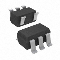
DBV PACKAGE
(TOP VIEW)
Supply 3 V to 30 V, or Dual Supplies
Class AB Output Stage
True Differential-Input Stage
Low Input Bias Current
Internal Frequency Compensation
Short-Circuit Protection
IN+
VCC−/GND
IN−
1
5
VCC+
4
OUT
2
3
description/ordering information
The TL343 is a single operational amplifier similar in performance to the µA741, but with several distinct
advantages. It is designed to operate from a single supply over a range of voltages from 3 V to 30 V. Operation
from split supplies also is possible, provided the difference between the two supplies is 3 V to 30 V. The
common-mode input range includes the negative supply. Output range is from the negative supply to
VCC − 1.5 V.
ORDERING INFORMATION
TA
VIOMAX
AT 25°C
−40°C to 125°C
10 mV
ORDERABLE
PART NUMBER
PACKAGE†
SOT-23-5 (DBV)
Reel of 3000
TL343IDBVR
Reel of 250
TL343IDBVT
TOP-SIDE
MARKING‡
T4I_
† Package drawings, standard packing quantities, thermal data, symbolization, and PCB design guidelines are available
at www.ti.com/sc/package.
‡ The actual top-side marking has one additional character that designates the assembly/test site.
symbol
−
IN−
+
IN+
OUT
Please be aware that an important notice concerning availability, standard warranty, and use in critical applications of
Texas Instruments semiconductor products and disclaimers thereto appears at the end of this data sheet.
Copyright 2005, Texas Instruments Incorporated
�
�����
� ���� ����������� �� ����!�� �� �� "�#$������� %��!&
��%���� ������� �� �"!����������� "!� �'! �!��� �� �!(�� �������!���
����%��% )������*&
��%������ "���!����+ %�!� ��� �!�!�����$* ���$�%!
�!����+ �� �$$ "����!�!��&
POST OFFICE BOX 655303
• DALLAS, TEXAS 75265
1
������
����� �
��
� �
����
��� ��
���� �
SLOS250G − JUNE 1999 − REVISED JANUARY 2005
schematic
VCC+
5 pF
IN+
OUT
IN−
2.4 kΩ
VCC−/GND
NOTE A: Component values shown are nominal.
absolute maximum ratings over operating free-air temperature range (unless otherwise noted)
MAX
VCC+
VCC−
Supply voltage (see Note 1)
Supply voltage, VCC+ with respect to VCC−
UNIT
18
−18
V
36
V
Differential input voltage (see Note 2)
±36
V
Input voltage (see Notes 1 and 3)
±18
V
Package thermal impedance, θJA (see Notes 4 and 5)
206
°C/W
150
°C
−65 to 150
°C
Operating virtual junction temperature, TJ
Storage temperature range, Tstg
NOTES: 1.
2.
3.
4.
These voltage values are with respect to the midpoint between VCC+ and VCC−.
Differential voltages are at IN+ with respect to IN−.
Neither input must ever be more positive than VCC+ or more negative than VCC−.
Maximum power dissipation is a function of TJ(max), θJA, and TA. The maximum allowable power dissipation at any allowable
ambient temperature is PD = (TJ(max) − TA)/θJA. Selecting the maximum of 150°C can affect reliability.
5. The package thermal impedance is calculated in accordance with JESD 51-7.
2
POST OFFICE BOX 655303
• DALLAS, TEXAS 75265
������
����� �
��
� �
����
��� ��
���� �
SLOS250G − JUNE 1999 − REVISED JANUARY 2005
recommended operating conditions
VCC
VCC+
VCC−
TA
Single-supply voltage
Dual-supply voltage
Operating free-air temperature
MIN
MAX
3
30
1.5
15
−1.5
−15
−40
125
UNIT
V
V
°C
electrical characteristics at specified free-air temperature, VCC± = ±15 V (unless otherwise noted)
TEST CONDITIONS†
PARAMETER
MIN
25°C
VIO
Input offset voltage
See Note 6
aV
Temperature coefficient
of input offset voltage
See Note 6
IIO
Input offset current
See Note 6
aI
Temperature coefficient
of input offset current
See Note 6
IIB
Input bias current
See Note 6
VICR
Common-mode input voltage range‡
VOM
Peak output-voltage swing
IO
IO
12
Full range
10
25°C
30
−200
VCC−
to 13
VCC−
to 13.5
25°C
±12
±13.5
25°C
±10
±13
Full range
±10
25°C
20
Full range
15
AVD
Large-signal differential
voltage amplification
VO = ±10 V,
RL = 2 kΩ
BOM
Maximum-output-swing bandwidth
VOPP = 20 V,
THD ≤ 5%,
AVD = 1,
RL = 2 kΩ
25°C
B1
φm
Unity-gain bandwidth
VO = 50 mV,
CL = 200 pF,
RL = 10 kΩ
Phase margin
RL = 2 kΩ
ri
Input resistance
f = 20 Hz
25°C
ro
Output resistance
f = 20 Hz
25°C
CMRR
Common-mode rejection ratio
25°C
kSVS
Supply-voltage sensitivity (∆VIO/∆VCC)
Short-circuit output current§
VIC = VICR(min)
VCC± = ±2.5 to ±15 V
−500
nA
V
V
200
V/mV
9
kHz
25°C
1
MHz
25°C
44
Deg
1
MΩ
0.3
75
Ω
70
90
dB
30
150
µV/V
±10
±30
±55
mA
0.7
2.8
25°C
25°C
mA
† All characteristics are measured under open-loop conditions, with zero common-mode voltage, unless otherwise specified. Full range for TA is
−40°C to 125°C.
‡ The VICR limits are linked directly, volt-for-volt, to supply voltage; the positive limit is 2 V less than VCC+.
§ Temperature and/or supply voltages must be limited to ensure that the dissipation rating is not exceeded.
NOTE 6: VIO, IIO, IIB, and ICC are defined at VO = 0.
POST OFFICE BOX 655303
See Note 6
nA
pA/°C
−800
25°C
mV
50
50
Full range
UNIT
µV/°C
200
Full range
RL = 2 kΩ
No load,
10
Full range
RL = 10 kΩ
Total supply current
MAX
2
Full range
25°C
IOS
ICC
TYP
• DALLAS, TEXAS 75265
25°C
3
������
����� �
��
� �
����
��� ��
���� �
SLOS250G − JUNE 1999 − REVISED JANUARY 2005
electrical characteristics, VCC+ = 3 V and 5 V, VCC− = 0 V, TA = 25°C (unless otherwise noted)
TEST CONDITIONS†
PARAMETER
VIO
IIO
Input offset voltage
IIB
VOM
Input bias current
MIN
VO = 1.5 V and 2.5 V
VO = 1.5 V and 2.5 V
Input offset current
Peak output voltage swing‡
VO = 1.5 V and 2.5 V
RL = 10 kΩ
AVD
Large-signal differential voltage
amplification
VO = 1.7 V to 3.3 V,
kSVS
Supply-voltage sensitivity (∆VIO/∆VCC±)
RL = 2 kΩ
TYP
MAX
UNIT
2
10
mV
30
50
nA
−200
−500
nA
3.3
3.5
V
20
200
V/mV
VCC± = ±2.5 V to ±15 V
VO = 1.5 V and 2.5 V,
150
ICC
Supply current
No load
0.7
1.75
† All characteristics are measured under open-loop conditions, with zero common-mode input voltage, unless otherwise specified.
‡ Output swings essentially to ground.
µV/V
mA
operating characteristics, VCC± = ±15 V, TA = 25°C, AVD = 1 (unless otherwise noted)
PARAMETER
TYP
UNIT
VI = ±10 V,
∆VO = 50 mV,
CL = 100 pF,
RL = 2 kΩ,
See Figure 1
1
V/µs
CL = 100 pF,
RL = 10 kΩ,
See Figure 1
0.35
µs
CL = 100 pF,
RL = 10 kΩ,
See Figure 1
0.35
µs
Overshoot factor
∆VO = 50 mV,
∆VO = 50 mV,
CL = 100 pF,
RL = 10 kΩ,
See Figure 1
20%
Crossover distortion
VI(PP) = 30 mV,
VOPP = 2 V,
f = 10 kHZ
SR
Slew rate at unity gain
tr
tf
Rise time
Fall time
TEST CONDITIONS
PARAMETER MEASUREMENT INFORMATION
+
−
VI
OUT
CL = 100 pF
RL
Figure 1. Unity-Gain Amplifier
4
POST OFFICE BOX 655303
• DALLAS, TEXAS 75265
1%
������
����� �
��
� �
����
��� ��
���� �
SLOS250G − JUNE 1999 − REVISED JANUARY 2005
TYPICAL CHARACTERISTICS†
INPUT BIAS CURRENT
vs
FREE-AIR TEMPERATURE
250
VCC± = ±15 V
TA = 25°C
200
I IB − Input Bias Current − nA
I IB − Input Bias Current − nA
250
INPUT BIAS CURRENT
vs
SUPPLY VOLTAGE
150
100
50
0
−75
−50
−25
0
25
50
75
100
200
150
100
50
0
125
0
2
TA − Free-Air Temperature − °C
RL = 10 kΩ
TA = 25°C
25
20
15
10
5
4
6
8
10
12
14
16
MAXIMUM PEAK-TO-PEAK OUTPUT VOLTAGE
vs
FREQUENCY
VOPP − Maximum Peak-to-Peak Output Voltage − V
VOPP − Maximum Peak-to-Peak Output Voltage − V
30
2
8
Figure 3
MAXIMUM PEAK-TO-PEAK OUTPUT VOLTAGE
vs
SUPPLY VOLTAGE
0
6
|VCC±| − Supply Voltage − V
Figure 2
0
4
10
12
14
16
ÎÎÎÎÎ
ÎÎÎÎÎ
ÎÎÎÎÎ
ÎÎÎÎÎ
ÎÎÎÎÎ
30
VCC± = ±15 V
CL = 0
RL = 10 kΩ
TA = 25°C
See Figure 1
25
20
15
10
5
0
1k
|VCC±| − Supply Voltage − V
10 k
100 k
1M
f − Frequency − Hz
Figure 4
Figure 5
† Operation of the device at these or any other conditions beyond those indicated under “recommended operating conditions” is not implied.
POST OFFICE BOX 655303
• DALLAS, TEXAS 75265
5
������
����� �
��
� �
����
��� ��
���� �
SLOS250G − JUNE 1999 − REVISED JANUARY 2005
106
LARGE-SIGNAL
DIFFERENTIAL VOLTAGE AMPLIFICATION
vs
FREQUENCY
ÎÎÎÎÎ
ÎÎÎÎÎ
ÎÎÎÎÎ
VOLTAGE-FOLLOWER
LARGE-SIGNAL PULSE RESPONSE
VCC± = ±15 V
RL = 2 kΩ
TA = 25°C
105
104
103
102
ÎÎÎÎÎ
ÎÎÎÎÎ
ÎÎÎÎÎ
VCC± = ±15 V
RL = 2 kΩ
TA = 25°C
See Figure 1
10
Input/Output Voltages − V
A VD − Large-Signal Differential Voltage Amplification − dB
TYPICAL CHARACTERISTICS†
Output
5
0
−5
10
Input
−10
1
1
10
100
1k
10 k
100 k
1M
0
10
20
30
40
50
60
70
80
90
t − Time − µs
f − Frequency − Hz
Figure 7
Figure 6
† Operation of the device at these or any other conditions beyond those indicated under “recommended operating conditions” is not implied.
6
POST OFFICE BOX 655303
• DALLAS, TEXAS 75265
�PACKAGE OPTION ADDENDUM
www.ti.com
29-Jan-2021
PACKAGING INFORMATION
Orderable Device
Status
(1)
Package Type Package Pins Package
Drawing
Qty
Eco Plan
(2)
Lead finish/
Ball material
MSL Peak Temp
Op Temp (°C)
(3)
Device Marking
(4/5)
(6)
TL343IDBVR
ACTIVE
SOT-23
DBV
5
3000
RoHS & Green
NIPDAU | SN
Level-1-260C-UNLIM
-40 to 125
(T4IG, T4IJ, T4IL,
T4IS)
TL343IDBVT
ACTIVE
SOT-23
DBV
5
250
RoHS & Green
NIPDAU | SN
Level-1-260C-UNLIM
-40 to 125
(T4IG, T4IJ, T4IL,
T4IU)
(1)
The marketing status values are defined as follows:
ACTIVE: Product device recommended for new designs.
LIFEBUY: TI has announced that the device will be discontinued, and a lifetime-buy period is in effect.
NRND: Not recommended for new designs. Device is in production to support existing customers, but TI does not recommend using this part in a new design.
PREVIEW: Device has been announced but is not in production. Samples may or may not be available.
OBSOLETE: TI has discontinued the production of the device.
(2)
RoHS: TI defines "RoHS" to mean semiconductor products that are compliant with the current EU RoHS requirements for all 10 RoHS substances, including the requirement that RoHS substance
do not exceed 0.1% by weight in homogeneous materials. Where designed to be soldered at high temperatures, "RoHS" products are suitable for use in specified lead-free processes. TI may
reference these types of products as "Pb-Free".
RoHS Exempt: TI defines "RoHS Exempt" to mean products that contain lead but are compliant with EU RoHS pursuant to a specific EU RoHS exemption.
Green: TI defines "Green" to mean the content of Chlorine (Cl) and Bromine (Br) based flame retardants meet JS709B low halogen requirements of


 工商网监
湘ICP备2023018690号
工商网监
湘ICP备2023018690号
