TL3472
HIGH-SLEW-RATE, SINGLE-SUPPLY OPERATIONAL AMPLIFIER
SLOS200G − OCTOBER 1997 − REVISED JULY 2003
D
D
D
D
D
D
D
D
D OR P PACKAGE
(TOP VIEW)
Wide Gain-Bandwidth Product . . . 4 MHz
High Slew Rate . . . 13 V/μs
Fast Settling Time . . . 1.1 μs to 0.1%
Wide-Range Single-Supply
Operation . . . 4 V to 36 V
Wide Input Common-Mode Range Includes
Ground (VCC−)
Low Total Harmonic Distortion . . . 0.02%
Large-Capacitance Drive
Capability . . . 10,000 pF
Output Short-Circuit Protection
1OUT
1IN−
1IN+
VCC−/GND
1
8
2
7
3
6
4
5
VCC+
2OUT
2IN−
2IN+
description/ordering information
Quality, low-cost, bipolar fabrication with innovative design concepts is employed for the TL3472 operational
amplifier. This device offers 4 MHz of gain-bandwidth product, 13-V/μs slew rate, and fast settling time, without
the use of JFET device technology. Although the TL3472 can be operated from split supplies, it is particularly
suited for single-supply operation because the common-mode input voltage range includes ground potential
(VCC−). With a Darlington transistor input stage, this device exhibits high input resistance, low input offset
voltage, and high gain. The all-npn output stage, characterized by no dead-band crossover distortion and large
output voltage swing, provides high-capacitance drive capability, excellent phase and gain margins, low
open-loop high-frequency output impedance, and symmetrical source/sink ac frequency response. This
low-cost amplifier is an alternative to the MC33072 and the MC34072 operational amplifiers.
ORDERING INFORMATION
PDIP (P)
0°C
0
C to 70°C
70 C
SOIC (D)
PDIP (P)
−40°C
40 C to 105
105°C
C
†
ORDERABLE
PART NUMBER
PACKAGE†
TA
SOIC (D)
Tube of 25
TL3472CP
Tube of 50
TL3472CD
Reel of 2500
TL3472CDR
Tube of 25
TL3472IP
Tube of 50
TL3472ID
Reel of 2500
TL3472IDR
TOP-SIDE
MARKING
TL3472CP
3472C
TL3472IP
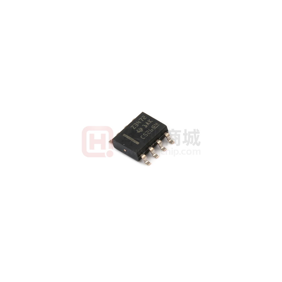
Z3472
Package drawings, standard packing quantities, thermal data, symbolization, and PCB design
guidelines are available at www.ti.com/sc/package.
Please be aware that an important notice concerning availability, standard warranty, and use in critical applications of
Texas Instruments semiconductor products and disclaimers thereto appears at the end of this data sheet.
Copyright © 2003, Texas Instruments Incorporated
PRODUCTION DATA information is current as of publication date.
Products conform to specifications per the terms of Texas Instruments
standard warranty. Production processing does not necessarily include
testing of all parameters.
POST OFFICE BOX 655303
• DALLAS, TEXAS 75265
1
�TL3472
HIGH-SLEW-RATE, SINGLE-SUPPLY OPERATIONAL AMPLIFIER
SLOS200G − OCTOBER 1997 − REVISED JULY 2003
schematic (each amplifier)
VCC+
OUT
IN−
IN+
VCC−/GND
2
POST OFFICE BOX 655303
• DALLAS, TEXAS 75265
�TL3472
HIGH-SLEW-RATE, SINGLE-SUPPLY OPERATIONAL AMPLIFIER
SLOS200G − OCTOBER 1997 − REVISED JULY 2003
absolute maximum ratings over operating free-air temperature range (unless otherwise noted)†
Supply voltage (see Note 1): VCC+ . . . . . . . . . . . . . . . . . . . . . . . . . . . . . . . . . . . . . . . . . . . . . . . . . . . . . . . . . . . 18 V
VCC− . . . . . . . . . . . . . . . . . . . . . . . . . . . . . . . . . . . . . . . . . . . . . . . . . . . . . . . . . . −18 V
Differential input voltage, VID (see Note 2) . . . . . . . . . . . . . . . . . . . . . . . . . . . . . . . . . . . . . . . . . . . . . . . . . . . . ±36 V
Input voltage, VI (any input) . . . . . . . . . . . . . . . . . . . . . . . . . . . . . . . . . . . . . . . . . . . . . . . . . . . . . . . . . . . . . . . . VCC±
Input current, II (each input) . . . . . . . . . . . . . . . . . . . . . . . . . . . . . . . . . . . . . . . . . . . . . . . . . . . . . . . . . . . . . . . ±1 mA
Output current, IO . . . . . . . . . . . . . . . . . . . . . . . . . . . . . . . . . . . . . . . . . . . . . . . . . . . . . . . . . . . . . . . . . . . . . . . ±80 mA
Total current into VCC+ . . . . . . . . . . . . . . . . . . . . . . . . . . . . . . . . . . . . . . . . . . . . . . . . . . . . . . . . . . . . . . . . . . . . 80 mA
Total current out of VCC− . . . . . . . . . . . . . . . . . . . . . . . . . . . . . . . . . . . . . . . . . . . . . . . . . . . . . . . . . . . . . . . . . . 80 mA
Duration of short-circuit current at (or below) 25°C (see Note 3) . . . . . . . . . . . . . . . . . . . . . . . . . . . . . . Unlimited
Package thermal impedance, θJA (see Notes 4 and 5): D package . . . . . . . . . . . . . . . . . . . . . . . . . . . . 97°C/W
P package . . . . . . . . . . . . . . . . . . . . . . . . . . . . 85°C/W
Operating virtual junction temperature, TJ . . . . . . . . . . . . . . . . . . . . . . . . . . . . . . . . . . . . . . . . . . . . . . . . . . . 150°C
Lead temperature 1.6 mm (1/16 inch) from case for 10 seconds . . . . . . . . . . . . . . . . . . . . . . . . . . . . . . . 260°C
Storage temperature range, Tstg . . . . . . . . . . . . . . . . . . . . . . . . . . . . . . . . . . . . . . . . . . . . . . . . . . . −65°C to 150°C
†
Stresses beyond those listed under “absolute maximum ratings” may cause permanent damage to the device. These are stress ratings only, and
functional operation of the device at these or any other conditions beyond those indicated under “recommended operating conditions” is not
implied. Exposure to absolute-maximum-rated conditions for extended periods may affect device reliability.
NOTES: 1. All voltage values, except differential voltages, are with respect to the midpoint between VCC+ and VCC−.
2. Differential voltages are at the noninverting input with respect to the inverting input. Excessive input current can flow when the input
is less than VCC− − 0.3 V.
3. The output can be shorted to either supply. Temperature and/or supply voltages must be limited to ensure that the maximum
dissipation rating is not exceeded.
4. Maximum power dissipation is a function of TJ(max), θJA, and TA. The maximum allowable power dissipation at any allowable
ambient temperature is PD = (TJ(max) − TA)/θJA. Operating at the absolute maximum TJ of 150°C can impact reliability.
5. The package thermal impedance is calculated in accordance with JESD 51-7.
recommended operating conditions
MIN
VCC±
Supply voltage
VIC
Common mode input voltage
Common-mode
TA
Operating free-air
free air temperature
VCC = 5 V
VCC± = ±15 V
TL3472C
TL3472I
POST OFFICE BOX 655303
• DALLAS, TEXAS 75265
MAX
4
36
0
2.8
−15
12.8
0
70
−40
105
UNIT
V
V
°C
3
�TL3472
HIGH-SLEW-RATE, SINGLE-SUPPLY OPERATIONAL AMPLIFIER
SLOS200G − OCTOBER 1997 − REVISED JULY 2003
electrical characteristics at specified free-air temperature, VCC± = ±15 V (unless otherwise noted)
PARAMETER
aV
IO
Input offset voltage
Temperature coefficient of
input offset voltage
VCC = ±15 V
VIC = 0,
VO = 0,
RS = 50 Ω
Input offset current
VCC = ±15 V
IIB
Input bias current
VCC = ±15 V
Common mode
Common-mode
input voltage range
High-level
High
level output voltage
Low-level
Low
level output voltage
AVD
Large signal differential
Large-signal
voltage amplification
IOS
Short circuit output current
Short-circuit
CMRR
10
range‡
VCC− = 0,
Full range‡
10
25°C
6
25°C
100
25°C
−15
to
12.8
Full range‡
−15
to
12.8
3.7
4
25°C
13.6
14
RL = 2 kΩ
Full range‡
13.4
V
0.3
RL = 10 kΩ
25°C
−14.7
−14.3
RL = 2 kΩ
Full range‡
25°C
RL = 2 kΩ
Source: VID = 1 V,
VO = 0
Sink: VID = −1 V,
VO = 0
Common mode rejection ratio
Common-mode
VIC = VICR(min),
(min)
RS = 50 Ω
kSVR
Supply-voltage rejection ratio
(ΔVCC±/ΔVIO)
VCC± = ±13.5 V to ±16.5 V,
ICC
Supply
pp y current (per
(p channel))
Full
RS = 100 Ω
100
V/mV
20
−34
20
27
25°C
65
97
dB
25°C
70
97
dB
mA
25°C
3.5
4.5
4.5
5.5
25°C
3.5
4.5
VCC+ = 5 V, VO = 2.5 V, VCC− = 0, No load
• DALLAS, TEXAS 75265
25
Full range‡
All typical values are at TA = 25°C.
‡ Full range is 0°C to 70°C for the TL3472C device and −40°C to 105°C for the TL3472I device.
V
−13.5
−10
25°C
No load
POST OFFICE BOX 655303
range‡
nA
V
0.1
VO = ±10 V
V,
nA
500
25°C
VO = 0
0,
RL = 2 kΩ
75
700
25°C
VCC− = 0,
mV
μV/°C
300
Full range‡
RL = 2 kΩ
UNIT
12
Full range‡
†
4
10
1.0
RL = 10 kΩ
VCC+ = 5 V,
VOL
1.5
25°C
MIN
RS = 50 Ω
VCC+ = 5 V,
VOH
25°C
Full
VCC = ±15 V
IIO
VICR
MAX
TA
VCC = 5 V
VIO
TYP†
TEST CONDITIONS
mA
�TL3472
HIGH-SLEW-RATE, SINGLE-SUPPLY OPERATIONAL AMPLIFIER
SLOS200G − OCTOBER 1997 − REVISED JULY 2003
operating characteristics, VCC± = ±15 V, TA = 25°C
PARAMETER
SR+
Positive slew rate
SR−
Negative slew rate
TEST CONDITIONS
VI = −10
10 V to 10 V,
RL = 2 kΩ, CL = 300 pF
AV = 1
MIN
TYP
8
MAX
UNIT
10
V/μs
AV = −1
13
V/μs
To 0.1%
1.1
To 0.01%
2.2
μss
ts
Settling time
AVD = −1,
1 10
10-V
V step
Vn
Equivalent input noise voltage
f = 1 kHz,
49
nV/√Hz
In
Equivalent input noise current
f = 1 kHz
0.22
pA/√Hz
THD
Total harmonic distortion
VO(PP) = 2 V to 20 V, RL = 2 kΩ, AVD = 10, f = 10 kHz
0.02
%
GBW
Gain-bandwidth product
f =100 kHz
BW
Power bandwidth
VO(PP) = 20 V
V, RL = 2 kΩ
kΩ, AVD = 1,
1 THD = 5.0%
5 0%
φm
RS = 100 Ω
3
4
MHz
160
kHz
CL = 0
70
CL = 300 pF
50
CL = 0
12
Phase margin
RL = 2 kΩ
Gain margin
RL = 2 kΩ
ri
Differential input resistance
VIC = 0
150
MΩ
Ci
Input capacitance
VIC = 0
2.5
pF
Channel separation
f = 10 kHz
101
dB
Open-loop output impedance
f = 1 MHz,
20
Ω
zo
POST OFFICE BOX 655303
CL = 300 pF
AV = 1
• DALLAS, TEXAS 75265
4
deg
dB
5
�PACKAGE OPTION ADDENDUM
www.ti.com
10-Dec-2020
PACKAGING INFORMATION
Orderable Device
Status
(1)
Package Type Package Pins Package
Drawing
Qty
Eco Plan
(2)
Lead finish/
Ball material
MSL Peak Temp
Op Temp (°C)
Device Marking
(3)
(4/5)
(6)
TL3472CD
ACTIVE
SOIC
D
8
75
RoHS & Green
NIPDAU
Level-1-260C-UNLIM
0 to 70
3472C
TL3472CDR
ACTIVE
SOIC
D
8
2500
RoHS & Green
NIPDAU
Level-1-260C-UNLIM
0 to 70
3472C
TL3472CP
ACTIVE
PDIP
P
8
50
RoHS & Green
NIPDAU
N / A for Pkg Type
0 to 70
TL3472CP
TL3472ID
ACTIVE
SOIC
D
8
75
RoHS & Green
NIPDAU
Level-1-260C-UNLIM
-40 to 105
Z3472
TL3472IDR
ACTIVE
SOIC
D
8
2500
RoHS & Green
NIPDAU
Level-1-260C-UNLIM
-40 to 105
Z3472
TL3472IP
ACTIVE
PDIP
P
8
50
RoHS & Green
NIPDAU
N / A for Pkg Type
-40 to 105
TL3472IP
(1)
The marketing status values are defined as follows:
ACTIVE: Product device recommended for new designs.
LIFEBUY: TI has announced that the device will be discontinued, and a lifetime-buy period is in effect.
NRND: Not recommended for new designs. Device is in production to support existing customers, but TI does not recommend using this part in a new design.
PREVIEW: Device has been announced but is not in production. Samples may or may not be available.
OBSOLETE: TI has discontinued the production of the device.
(2)
RoHS: TI defines "RoHS" to mean semiconductor products that are compliant with the current EU RoHS requirements for all 10 RoHS substances, including the requirement that RoHS substance
do not exceed 0.1% by weight in homogeneous materials. Where designed to be soldered at high temperatures, "RoHS" products are suitable for use in specified lead-free processes. TI may
reference these types of products as "Pb-Free".
RoHS Exempt: TI defines "RoHS Exempt" to mean products that contain lead but are compliant with EU RoHS pursuant to a specific EU RoHS exemption.
Green: TI defines "Green" to mean the content of Chlorine (Cl) and Bromine (Br) based flame retardants meet JS709B low halogen requirements of


 工商网监
湘ICP备2023018690号
工商网监
湘ICP备2023018690号

