�����
���
�����
�� ��� �����
SLVS050D − JUNE 1976 − REVISED JANUARY 2005
D
D
D
D
D
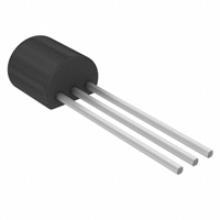
LP PACKAGE
(TOP VIEW)
Temperature Compensated
Programmable Output Voltage
Low Output Resistance
Low Output Noise
Sink Capability up to 100 mA
CATHODE
ANODE
REF
description/ordering information
The TL430 is a 3-terminal adjustable shunt regulator, featuring excellent temperature stability, wide operating
current range, and low output noise. The output voltage can be set by two external resistors to any desired value
between 3 V and 30 V. The TL430 can replace Zener diodes in many applications, providing improved
performance.
The TL430C is characterized for operation from 0°C to 70°C.
ORDERING INFORMATION
0°C to 70°C
ORDERABLE
PART NUMBER
PACKAGE†
TA
TO-226 / TO-92 (LP)
Bulk of 1000
TL430CLP
Reel of 2000
TL430CLPR
TOP-SIDE
MARKING
TL430C
† Package drawings, standard packing quantities, thermal data, symbolization, and PCB design
guidelines are available at www.ti.com/sc/package.
symbol
REF
ANODE
CATHODE
Please be aware that an important notice concerning availability, standard warranty, and use in critical applications of
Texas Instruments semiconductor products and disclaimers thereto appears at the end of this data sheet.
Copyright 2005, Texas Instruments Incorporated
���� ����� ���� ����������� �� ����!�� �� �� "�#$������� %��!&
���%���� ������� �� �"!����������� "!� �'! �!��� �� �!(�� �������!���
����%��% )������*& ���%������ "���!����+ %�!� ��� �!�!�����$* ���$�%!
�!����+ �� �$$ "����!�!��&
POST OFFICE BOX 655303
• DALLAS, TEXAS 75265
1
������
���
�����
�� ��� �����
SLVS050D − JUNE 1976 − REVISED JANUARY 2005
absolute maximum ratings over operating free-air temperature range (unless otherwise noted)†
Regulator voltage (see Note 1) . . . . . . . . . . . . . . . . . . . . . . . . . . . . . . . . . . . . . . . . . . . . . . . . . . . . . . . . . . . . . . 30 V
Continuous regulator current . . . . . . . . . . . . . . . . . . . . . . . . . . . . . . . . . . . . . . . . . . . . . . . . . . . . . . . . . . . . . 150 mA
Package thermal impedance, θJA (see Notes 2 and 3)
. . . . . . . . . . . . . . . . . . . . . . . . . . . . . . . . . . . . 140°C/W
Operating virtual junction temperature, TJ . . . . . . . . . . . . . . . . . . . . . . . . . . . . . . . . . . . . . . . . . . . . . . . . . . . 150°C
Lead temperature 1,6 mm (1/16 inch) from case for 10 seconds . . . . . . . . . . . . . . . . . . . . . . . . . . . . . . . 260°C
Storage temperature range, Tstg . . . . . . . . . . . . . . . . . . . . . . . . . . . . . . . . . . . . . . . . . . . . . . . . . . . −65°C to 150°C
† Stresses beyond those listed under “absolute maximum ratings” may cause permanent damage to the device. These are stress ratings only, and
functional operation of the device at these or any other conditions beyond those indicated under “recommended operating conditions” is not
implied. Exposure to absolute-maximum-rated conditions for extended periods may affect device reliability.
NOTES: 1. All voltage values are with respect to the anode terminal.
2. Maximum power dissipation is a function of TJ(max), θJA, and TA. The maximum allowable power dissipation at any allowable
ambient temperature is PD = (TJ(max) − TA)/θJA. Operating at the absolute maximum TJ of 150°C can impact reliability.
3. The package thermal impedance is calculated in accordance with JESD 51-7.
recommended operating conditions
VZ
IZ
Regulator voltage
TA
Operating free-air temperature range
Regulator current
TL430C
MIN
MAX
Vref
2
30
UNIT
V
100
mA
0
70
°C
electrical characteristics over recommended operating conditions, TA = 25°C (unless otherwise
noted)
TEST
FIGURE
PARAMETER
TEST CONDITIONS
VI(ref)
Reference input voltage
1
VZ = VI(ref),
VZ = VI(ref),
TA = 0°C to 70°C
IZ = 10 mA
IZ = 10 mA,
αVI(ref)
Temperature coefficient of reference input
voltage
1
II(ref)
Reference input current
2
IZ = 10 mA,
R2 = ∞
R1 = 10 kΩ,
IZK
Regulator current near lower knee of
regulation range
1
VZ = VI(ref)
IZK
Regulator current at maximum
limit of regulation range
1
VZ = VI(ref)
VZ = 5 V to 30 V,
rz
Differential regulator resistance
(see Note 5)
1
VZ = VI(ref),
∆IZ = (52 − 2) mA
Vn
Noise voltage
2
f = 0.1 Hz to 10 Hz
2
TL430C
MIN
TYP
MAX
2.5
2.75
3
120
UNIT
V
ppm/°C
3
10
µA
0.5
2
mA
50
See Note 4
mA
100
1.5
VZ = 3 V
VZ = 12 V
3
Ω
50
200
µV
VZ = 30 V
650
NOTES: 4. The average power dissipation, VZ • IZ • duty cycle, must not exceed the maximum continuous rating in any 10-ms interval.
5. The regulator resistance for VZ > VI(ref), rz, is given by:
ǒ
r zȀ + r z 1 ) R1
R2
2
Ǔ
POST OFFICE BOX 655303
• DALLAS, TEXAS 75265
������
���
�����
�� ��� �����
SLVS050D − JUNE 1976 − REVISED JANUARY 2005
PARAMETER MEASUREMENT INFORMATION
Input
VZ
IZ
Input
R1
VZ
II(ref)
IZ
TL430
R2
VI(ref)
TL430
VI(ref)
V
Figure 1. Test Circuit for VZ = VI(ref)
POST OFFICE BOX 655303
Z
+ V
I(ref)
ǒ1 ) R1
Ǔ ) II(ref)
R2
R1
Figure 2. Test Circuit for VZ > VI(ref)
• DALLAS, TEXAS 75265
3
������
���
�����
�� ��� �����
SLVS050D − JUNE 1976 − REVISED JANUARY 2005
TYPICAL CHARACTERISTICS
SMALL-SIGNAL REGULATOR IMPEDANCE
vs
FREQUENCY
CATHODE CURRENT
vs
CATHODE VOLTAGE
160
VZ = VI(ref)
TA = 25°C
2.8
2.6
2.4
2.2
2
1.8
100
80
IZ
60
40
20
1.4
0
102
103
104
105
106
IZM
120
1.6
10
VZ = VI(ref)
TA = 25°C
140
I − Cathode Current − mA
z z − Small-Signal Regulator Impedance − Ω
3
IZK
0
1
f − Frequency − Hz
3
2
4
V − Cathode Voltage − V
Figure 3
Figure 4
APPLICATION INFORMATION
V+
R
V+
VO
30 Ω
R1
4.7 kΩ
VI(ref)
R2
R1
R2
V
O
[
ǒ1 ) R1
Ǔ VI(ref)
R2
V
Figure 5. Shunt Regulator
4
POST OFFICE BOX 655303
O
[
ǒ1 ) R1
Ǔ VI(ref)
R2
Figure 6. Series Regulator
• DALLAS, TEXAS 75265
VO
������
���
�����
�� ��� �����
SLVS050D − JUNE 1976 − REVISED JANUARY 2005
APPLICATION INFORMATION
V+
µA7805 Regulator
IN
VO
OUT
GND
RCL
IO
V+
R1
R2
I
O
[
I(ref)
R
CL
Min V
Figure 7. Current Limiter
V+
ǒ1 ) R1
Ǔ VI(ref)
R2
O
+
O
+ V
V
V
I(ref)
) 5V
Figure 8. Output Control of a 3-Terminal
Fixed Regulator
VO
V+
VO
R1
R1
R2
Q1
R2
V
O
[
ǒ1 ) R1
Ǔ VI(ref)
R2
V
limit
[
Figure 9. Higher-Current Applications
ǒ1 ) R1
Ǔ ǒVI(ref) ) VBE(Q1)Ǔ
R2
Figure 10. Crowbar
VCC
R1B
R1A
Low limit [ V
R2A
R2B
I(ref)
High limit [ V
I(ref)
ǒ1 ) R1B
Ǔ ) VD
R2B
ǒ1 ) R1A
Ǔ
R2A
Figure 11. VCC Monitor
POST OFFICE BOX 655303
• DALLAS, TEXAS 75265
5
�PACKAGE OPTION ADDENDUM
www.ti.com
25-Sep-2021
PACKAGING INFORMATION
Orderable Device
Status
(1)
Package Type Package Pins Package
Drawing
Qty
Eco Plan
(2)
Lead finish/
Ball material
MSL Peak Temp
Op Temp (°C)
Device Marking
(3)
(4/5)
(6)
TL430CLP
ACTIVE
TO-92
LP
3
1000
RoHS & Green
SN
N / A for Pkg Type
0 to 70
TL430C
TL430CLPE3
ACTIVE
TO-92
LP
3
1000
RoHS & Green
SN
N / A for Pkg Type
0 to 70
TL430C
(1)
The marketing status values are defined as follows:
ACTIVE: Product device recommended for new designs.
LIFEBUY: TI has announced that the device will be discontinued, and a lifetime-buy period is in effect.
NRND: Not recommended for new designs. Device is in production to support existing customers, but TI does not recommend using this part in a new design.
PREVIEW: Device has been announced but is not in production. Samples may or may not be available.
OBSOLETE: TI has discontinued the production of the device.
(2)
RoHS: TI defines "RoHS" to mean semiconductor products that are compliant with the current EU RoHS requirements for all 10 RoHS substances, including the requirement that RoHS substance
do not exceed 0.1% by weight in homogeneous materials. Where designed to be soldered at high temperatures, "RoHS" products are suitable for use in specified lead-free processes. TI may
reference these types of products as "Pb-Free".
RoHS Exempt: TI defines "RoHS Exempt" to mean products that contain lead but are compliant with EU RoHS pursuant to a specific EU RoHS exemption.
Green: TI defines "Green" to mean the content of Chlorine (Cl) and Bromine (Br) based flame retardants meet JS709B low halogen requirements of
很抱歉,暂时无法提供与“TL430CLPR”相匹配的价格&库存,您可以联系我们找货
免费人工找货- 国内价格 香港价格
- 2000+4.902872000+0.63426
- 4000+4.779524000+0.61831
- 6000+4.717736000+0.61031
- 10000+4.6492910000+0.60146
- 14000+4.6092914000+0.59629