��������
��
���
���
��������
SGLS268 − OCTOBER 2004
D Controlled Baseline
D
D
D
D
D
D
D
D
D
NS PACKAGE
(TOP VIEW)
− One Assembly/Test Site, One Fabrication
Site
Extended Temperature Performance of
−55°C to 125°C
Enhanced Diminishing Manufacturing
Sources (DMS) Support
Enhanced Product-Change Notification
Qualification Pedigree†
Excellent Dynamic Range
Wide Bandwidth
Built-In Temperature Compensation
Log Linearity (30-dB Sections) . . . 1 dB Typ
Wide Input Voltage Range
CA2
VCC −
CA2′
A1
Y
Y
A2
VCC +
1
16
2
15
3
14
4
13
5
12
6
11
7
10
8
9
NC
CB2
CB2′
GND
B1
Z
Z
B2
NC — No internal connection
† Component qualification in accordance with JEDEC and industry
standards to ensure reliable operation over an extended
temperature range. This includes, but is not limited to, Highly
Accelerated Stress Test (HAST) or biased 85/85, temperature
cycle, autoclave or unbiased HAST, electromigration, bond
intermetallic life, and mold compound life. Such qualification
testing should not be viewed as justifying use of this component
beyond specified performance and environmental limits.
DESCRIPTION
This amplifier circuit contains four 30-dB logarithmic stages. Gain in each stage is such that the output of each
stage is proportional to the logarithm of the input voltage over the 30-dB input voltage range. Each half of the
circuit contains two of these 30-dB stages summed together in one differential output that is proportional to the
sum of the logarithms of the input voltages of the two stages. The four stages may be interconnected to obtain
a theoretical input voltage range of 120-dB. In practice, this permits the input voltage range typically to be greater
than 80-dB with log linearity of ±0.5-dB (see application data). Bandwidth is from dc to 40 MHz.
This circuit is useful in data compression and analog compensation. This logarithmic amplifier is used in log IF
circuitry as well as video and log amplifiers.
The TL441M is characterized for operation over the full military temperature range of −55°C to 125°C.
ORDERING INFORMATION
TA
PACKAGE†
ORDERABLE
PART NUMBER
TOP-SIDE
MARKING
−55°C to 125°C
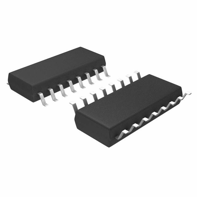
SOP (NS)
Tape and reel
TL441MNSREP
TL441MEP
† Package drawings, standard packing quantities, thermal data, symbolization, and PCB design guidelines
are available at www.ti.com/sc/package.
Please be aware that an important notice concerning availability, standard warranty, and use in critical applications of
Texas Instruments semiconductor products and disclaimers thereto appears at the end of this data sheet.
Copyright 2004, Texas Instruments Incorporated
���������� �
�
����������� �� ������� �� �� !�"#������� $���%
���$���� ������� �� �!������������ !�� �&� ����� �� ��'�� �����������
����$��$ (������)% ���$������ !��������* $��� ��� ���������#) ���#�$�
������* �� �## !���������%
POST OFFICE BOX 655303
• DALLAS, TEXAS 75265
1
���������
��
���
���
��������
SGLS268 − OCTOBER 2004
FUNCTIONAL LOGIC DIAGRAM (one half)
A1
(B1)
Log
Σ
−15 dB
Log
Y (Z)
Log
Y (Z)
CA2
(CB2)
A2
(B2)
−15 dB
Log
CA2′
(CB2′)
Y ∝ log A1 + log A2; Z ∝ log B1 + log B2 where: A1, A2, B1, and B2 are in dBV, 0 dBV = 1 V.
CA2, CA2′, CB2, and CB2′ are detector compensation inputs.
SCHEMATIC
VCC +
Y
Y
A2
A1
8
6
10
5
11
7
9
4
12
13
CA2′
CA2
VCC −
2
3
14
1
15
2
POST OFFICE BOX 655303
• DALLAS, TEXAS 75265
Z
Z
B2
B1
GND
CB2′
CB2
���������
��
���
���
��������
SGLS268 − OCTOBER 2004
ABSOLUTE MAXIMUM RATINGS OVER OPERATING FREE-AIR TEMPERATURE RANGE (unless
otherwise noted)†
TL441−EP
VCC+
VCC−
8V
Supply voltages (see Note 1)
−8 V
Input voltage (see Note 1)
θJA
6V
Output sink current (any one output)
30 mA
Package thermal impedance (see Notes 2 and 3)
83°C/W
Lead temperature 1,6 mm (1/16 inch) from case for 10 seconds
Tstg
260°C
Storage temperature range (see Note 4)
−65°C to 150°C
† Stresses beyond those listed under “absolute maximum ratings” may cause permanent damage to the device. These are stress ratings only, and
functional operation of the device at these or any other conditions beyond those indicated under “recommended operating conditions” is not
implied. Exposure to absolute-maximum-rated conditions for extended periods may affect device reliability.
NOTES: 1. All voltages, except differential out voltages, are with respect to network ground terminal.
2. Maximum power dissipation is a function of TJ(max), θJA, and TA. The maximum allowable power dissipation at any allowable
ambient temperature is PD = (TJ(max) − TA)/θJA. Operating at the absolute maximum TJ of 150°C can affect reliability.
3. The package thermal impedance is calculated in accordance with JESD 51-7.
4. Long-term high-temperature storage and/or extended use at maximum recommended operating conditions may result in a reduction
of overall device life. See http://www.ti.com/ep_quality for additional information on enhanced plastic packaging.
RECOMMENDED OPERATING CONDITIONS
MIN
MAX
UNIT
Peak-to-peak input voltage for each 30-dB stage
0.01
1
V
Operating free-air temperature, TA
−55
125
°C
TYP
MAX
UNIT
mV
ELECTRICAL CHARACTERISTICS, VCC± = ±6 V, TA = 255C
TEST
FIGURE
PARAMETER
MIN
Differential output offset voltage
1
±25
±70
Quiescent output voltage
2
5.45
5.6
5.85
DC scale factor (differential output), each 3-dB stage, −35 dBV to −5 dBV
3
7
8
11
AC scale factor (differential output)
8
DC error at −20 dBV (midpoint of −35 dBV to −5 dBV range)
3
1
Input impedance
mV/dB
2.6
Ω
200
Rise time, 10% to 90% points, CL = 24 pF
4
Supply current from VCC+
2
14.5
Supply current from VCC−
2
−6
Power dissipation
2
123
POST OFFICE BOX 655303
• DALLAS, TEXAS 75265
20
dB
Ω
500
Output impedance
V
mV/dB
35
ns
18.5
23
mA
−8.5
−10.5
mA
162
201
mW
3
���������
��
���
���
��������
SGLS268 − OCTOBER 2004
ELECTRICAL CHARACTERISTICS OVER OPERATING FREE-AIR TEMPERATURE RANGE,
VCC± = ±6 V (unless otherwise noted)
PARAMETER
TEST FIGURE
MIN
MAX
UNIT
±125
mV
Differential output offset voltage
1
Quiescent output voltage
2
5.3
5.85
DC scale factor (differential output) each 30-dB stage, −35 dBV to −5 dBV
3
6
11
DC error at −20 dBV (midpoint of −35 dBV to −5 dBV range)
TA = −55°C
TA = 125°C
V
mV/dB
4
3
3
dB
Supply current from VCC+
2
10
31
mA
Supply current from VCC−
2
−4.5
−15
mA
Power dissipation
2
87
276
mW
PARAMETER MEASUREMENT INFORMATION
VCC+
ICC +
VCC−
VCC+
VCC−
ICC −
CA2 CA2′ VCC+ VCC−
Y
A1
CA2 CA2′ VCC + VCC −
Y
A1
A2
B1
Y
B2
Z
DVM
Z
Y
A2
B1
Z
B2
Z
CB2 CB2′ GND
CB2 CB2′ GND
VO
PD = VCC+
Figure 1
4
•
ICC+ + VCC−
Figure 2
POST OFFICE BOX 655303
• DALLAS, TEXAS 75265
•
ICC−
���������
��
���
���
��������
SGLS268 − OCTOBER 2004
VCC+
VCC−
CA2 CA2′ VCC+ VCC−
Y
A1
Y
A2
B1
Z
B2
18 mV
100 mV
560 mV
DC
Power
Supply
DVM
Z
Scale Factor +
CB2 CB2′ GND
ƪVout(560 mV)–Vout(18mV)ƫ mV
Error +
30 dBV
ƪVout(100 mV)–0.5 Vout(560 mV)–0.5 Vout(18 mV)ƫ
Scale Factor
Figure 3
VCC+
CI
Atten
100 mV
0 mV
Pulse
Generator
50 Ω
VCC−
1000 pF
CA2 CA2′ VCC+ VCC−
Y
A1
Y
A2
B1
Z
B2
Tektronix
Sampling Scope
With Digital
Readout or
Equivalent
Z
CB2 CB2′
GND
CL
CL
NOTES: A. The input pulse has the following characteristics: tw = 200 ns, tr ≤ 2 ns, tf ≤ 2 ns, PRR ≤ 10 MHz.
B. Capacitor CI consists of three capacitors in parallel: 1 µF, 0.1 µF, and 0.01 µF.
C. CL includes probe and jig capacitance.
Figure 4
POST OFFICE BOX 655303
• DALLAS, TEXAS 75265
5
���������
��
���
���
��������
SGLS268 − OCTOBER 2004
TYPICAL CHARACTERISTICS
QUIESCENT OUTPUT VOLTAGE
vs
FREE-AIR TEMPERATURE
DIFFERENTIAL OUTPUT OFFSET VOLTAGE
vs
FREE-AIR TEMPERATURE
8
7
50
Quiescent Output Voltage − V
Differential Output Offset Voltage − mV
60
40
30
20
10
VCC ± = ± 6 V
See Figure 1
0
− 75 − 50 − 25
6
5
4
3
2
1
0
25
50
75
100
0
− 75 − 50 − 25
125
Figure 5
DC Error at Midpoint of 30-dBV Range − dBV
DC Scale Factor (Differential Output) − mV/dBV
10
8
6
4
VCC ± = ± 6 V
See Figure 3
25
75
100
125
50
75
100
125
2.0
1.8
1.6
1.4
1.2
1.0
0.8
0.6
0.4
0.2
VCC ± = ± 6 V
See Figure 3
0
− 75 − 50 − 25
TA − Free-Air Temperature − °C
0
25
Figure 8
POST OFFICE BOX 655303
50
75
100
TA − Free-Air Temperature − °C
Figure 7
6
50
DC ERROR
vs
FREE-AIR TEMPERATURE
12
0
25
Figure 6
DC SCALE FACTOR
vs
FREE-AIR TEMPERATURE
0
− 75 − 50 − 25
0
TA − Free-Air Temperature − °C
TA − Free-Air Temperature − °C
2
VCC ± = ± 6 V
See Figure 2
• DALLAS, TEXAS 75265
125
���������
��
���
���
��������
SGLS268 − OCTOBER 2004
OUTPUT RISE TIME
vs
LOAD CAPACITANCE
t r − Output Rise Time − ns
25
20
15
10
VCC ± = ± 6 V
TA = 25°C
See Figure 4, outputs
loaded symmetrically
5
0
0
5
10
15
20
25
CL − Load Capacitance − pF
30
Figure 9
POST OFFICE BOX 655303
• DALLAS, TEXAS 75265
7
���������
��
���
���
��������
SGLS268 − OCTOBER 2004
APPLICATION INFORMATION
Although designed for high-performance applications such as infrared detection, this device has a wide range
of applications in data compression and analog computation.
Basic Logarithmic Function
Functional Block Diagram
The basic logarithmic response is derived from
the exponential current-voltage relationship of
collector current and base-emitter voltage. This
relationship is given in the equation:
INPUT
A1
Log
−15 dB
m • VBE = In [(IC + ICES)/ICES]
where:
INPUT
B1
Log
−15 dB
Log
Log
CB2
CA2
IC =
ICES =
m =
VBE =
INPUT
A2
collector current
collector current at VBE = 0
Log
−15 dB
q/kT (in V − 1)
−15 dB
Log
base-emitter voltage
Log
Σ
CA2’
The differential input amplifier allows dual-polarity
inputs, is self-compensating for temperature
variations, and is relatively insensitive to
common-mode noise.
INPUT
B2
Log
Y
Σ
Y
Z
CB2’
Z
Outputs
Figure 10
Logarithmic Sections
As can be seen from the schematic, there are eight differential pairs. Each pair is a 15-dB log subsection, and
each input feeds two pairs, for a range of 30-dB per stage.
Four compensation points are available to allow slight variations in the gain (slope) of the two individual 15-dB
stages of input A2 and B2. By slightly changing the voltage on any of the compensation pins from their quiescent
values, the gain of that particular 15-dB stage can be adjusted to match the other 15-dB stage in the pair. The
compensation pins also can be used to match the transfer characteristics of input A2 to A1 or B2 to B1.
The log stages in each half of the circuit are summed by directly connecting their collectors together and
summing through a common-base output stage. The two sets of output collectors are used to give two log
outputs, Y and Y (or Z and Z), which are equal in amplitude, but opposite in polarity. This increases the versatility
of the device.
By proper choice of external connections, linear amplification, and linear attenuation many different applications
requiring logarithmic signal processing are possible.
Input Levels
The recommended input voltage range of any one stage is given as 0.01 V to 1 V. Input levels in excess of
1 V may result in a distorted output. When several log sections are summed together, the distorted area of one
section overlaps with the next section and the resulting distortion is insignificant. However, there is a limit to the
amount of overdrive that can be applied. As the input drive reaches ± 3.5 V, saturation occurs, clamping the
collector-summing line and severely distorting the output. Therefore, the signal to any input must be limited to
approximately ± 3 V to ensure a clean output.
8
POST OFFICE BOX 655303
• DALLAS, TEXAS 75265
���������
��
���
���
��������
SGLS268 − OCTOBER 2004
Output Levels
Differential-output-voltage levels are low, generally less than 0.6 V. As demonstrated in Figure 11, the output
swing and the slope of the output response can be adjusted by varying the gain by means of the slope control.
The coordinate origin also can be adjusted by positioning the offset of the output buffer.
Circuits
Figure 11 through Figure 18 show typical circuits using this logarithmic amplifier. Operational amplifiers not
otherwise designated are TLC271. For operation at higher frequencies, the TL592 is recommended instead of
the TLC271.
TYPICAL TRANSFER CHARACTERISTICS
1.4
1.2
Output Voltage − V
1.0
Adjusted for Increased
Slope and Offset
0.8
0.6
0.4
0.2
Adjusted For Minimum
Slope With Zero Offset
0
− 0.2
10 − 4
10 −3
10 −2
10 −1
1
101
Input Voltage − V
A1
−
+
Y
Origin
1/2
TL441
+
−
Input
A2 GND
Output
Y
Slope
Figure 11. Output Slope and Origin Adjustment
POST OFFICE BOX 655303
• DALLAS, TEXAS 75265
9
���������
��
���
���
��������
SGLS268 − OCTOBER 2004
TRANSFER CHARACTERISTICS of TWO
TYPICAL INPUT STAGES
0.4
Output Voltage − V
0.3
0.2
0.1
0
0.001
1
0.1
0.01
10
Input Voltage − V
2 kΩ, 1%
B1
2 kΩ, 1%
Z
20 kΩ
1/2
TL441
+
−
Output
2 kΩ, 1%
Input
B2 GND
Z
2 kΩ, 1%
Figure 12. Utilization of Separate Stages
10
POST OFFICE BOX 655303
• DALLAS, TEXAS 75265
���������
��
���
���
��������
SGLS268 − OCTOBER 2004
TRANSFER CHARACTERISTICS
WITH BOTH SIDES PARALLELED
0.4
Output Voltage − V
0.3
0.2
0.1
0
0.001
0.01
1
0.1
10
Input Voltage − V
2 kΩ, 1%
A1
Y
A2
20 kΩ
TL441
Input
2 kΩ, 1%
Y
−
Z
B1
+
Output
2 kΩ, 1%
B2
GND
Z
2 kΩ, 1%
Figure 13. Utilization of Paralleled Inputs
POST OFFICE BOX 655303
• DALLAS, TEXAS 75265
11
���������
��
���
���
��������
SGLS268 − OCTOBER 2004
TRANSFER CHARACTERISTICS
0.8
0.7
Output Voltage − V
0.6
0.5
0.4
0.3
0.2
0.1
0
10 − 4
10 −3
10 −2
10 −1
1
101
Input Voltage − V
2 kΩ
A1
Y
A2
Y
VCC + = 4 V
1 kΩ
15 kΩ
+
−
VCC − = − 4 V
5 kΩ
1 kΩ
20 kΩ
910 Ω
B1
Z
B2
Z
+
−
VCC + = 4 V
2 kΩ
+
−
100 Ω
Origin
TL441
910 Ω
Input
2 kΩ
Slope
5 kΩ
VCC − = − 4 V
5 kΩ
100 Ω
NOTES: A. nputs are limited by reducing the supply voltages for the input amplifiers to ± 4 V.
B. The gains of the input amplifiers are adjusted to achieve smooth transitions.
Figure 14. Logarithmic Amplifier With Input Voltage Range Greater Than 80 dB
12
POST OFFICE BOX 655303
• DALLAS, TEXAS 75265
Output
���������
��
���
���
��������
SGLS268 − OCTOBER 2004
R
A1
Y
TL441
A2
+
Input
A
−
R
R
R
R
+
Y
see
Note A
+
−
R
B1
+
B2
−
Y
1/2
TL441
A2
Y
+
−
Z
Input
B
OUTPUT W
(see Note B)
A1
−
Z
R
R
R
R
NOTES: A. Connections shown are for multiplication. For division, Z and Z connections are reversed.
B. Output W may need to be amplified to give actual product or quotient of A and B.
C. R designates resistors of equal value, typically 2 kΩ to 10 kΩ.
Multiplication: W = A • B ⇒ log W = log A + log B, or W = a(logaA + logaB)
Division: W = A/B ⇒ log W = log A − log B, or W = a(logaA + logaB)
Figure 15. Multiplication or Division
R
A1
Input
A
1/2
TL441
+
−
A2
nR
R
R
Y
−
R
+
−
B1
+
Y
+
−
B2
1/2
TL441
Z
Output
W
Z
R
nR
R
NOTE: R designates resistors of equal value, typically 2 kΩ to 10 kΩ. The power to which the input variable is raised is fixed by setting nR.
Output W may need to be amplified to give the correct value.
Exponential: W = An ⇒ log W = n log A, or W = a(n loga A)
Figure 16. Raising a Variable to a Fixed Power
POST OFFICE BOX 655303
• DALLAS, TEXAS 75265
13
���������
��
���
���
��������
SGLS268 − OCTOBER 2004
2 kΩ
Input
A
2 kΩ
Slope
Origin
−
A1
+
20 kΩ
+
A2
1/2
TL441
Y
Output
W
Y
−
2 kΩ
2 kΩ
NOTE: Adjust the slope to correspond to the base “a”. Exponential to any base: W = a.
Figure 17. Raising a Fixed Number to a Variable Power
2.2 kΩ
A1
Input
1
TL592
+
−
0.2 µF
0.2 µF
+
−
0.2 µF
2.2 kΩ
1 kΩ
50 Ω
TL441
TL592
Z
20 kΩ
B2
+
−
Open
0.2 µF
50 Ω
Output
1
1 kΩ
Gain Adj.
2.2 kΩ
B1
50 Ω
TL592
Y
Gain Adj. = 400 Ω
For 30 dB
Input
2
20 kΩ
A2
Open
50 Ω
Y
TL592
0.2 µF
+
−
0.2 µF
Output
2
Z
CA2 CA2’ CB2 CB2’
10
10
kΩ
kΩ
2.2 kΩ
1 kΩ
1 kΩ
Gain Adj.
Gain Adj. = 400 Ω
For 30 dB
VCC −
Figure 18. Dual-Channel RF Logarithmic Amplifier With 50-dB Input Range Per Channel at 10 MHz
14
POST OFFICE BOX 655303
• DALLAS, TEXAS 75265
�PACKAGE OPTION ADDENDUM
www.ti.com
10-Dec-2020
PACKAGING INFORMATION
Orderable Device
Status
(1)
Package Type Package Pins Package
Drawing
Qty
Eco Plan
(2)
Lead finish/
Ball material
MSL Peak Temp
Op Temp (°C)
Device Marking
(3)
(4/5)
(6)
TL441MNSREP
ACTIVE
SO
NS
16
2000
RoHS & Green
NIPDAU
Level-1-260C-UNLIM
-55 to 125
TL441MEP
V62/05603-01XE
ACTIVE
SO
NS
16
2000
RoHS & Green
NIPDAU
Level-1-260C-UNLIM
-55 to 125
TL441MEP
(1)
The marketing status values are defined as follows:
ACTIVE: Product device recommended for new designs.
LIFEBUY: TI has announced that the device will be discontinued, and a lifetime-buy period is in effect.
NRND: Not recommended for new designs. Device is in production to support existing customers, but TI does not recommend using this part in a new design.
PREVIEW: Device has been announced but is not in production. Samples may or may not be available.
OBSOLETE: TI has discontinued the production of the device.
(2)
RoHS: TI defines "RoHS" to mean semiconductor products that are compliant with the current EU RoHS requirements for all 10 RoHS substances, including the requirement that RoHS substance
do not exceed 0.1% by weight in homogeneous materials. Where designed to be soldered at high temperatures, "RoHS" products are suitable for use in specified lead-free processes. TI may
reference these types of products as "Pb-Free".
RoHS Exempt: TI defines "RoHS Exempt" to mean products that contain lead but are compliant with EU RoHS pursuant to a specific EU RoHS exemption.
Green: TI defines "Green" to mean the content of Chlorine (Cl) and Bromine (Br) based flame retardants meet JS709B low halogen requirements of