TLC2272-Q1, TLC2272A-Q1, TLC2274-Q1, TLC2274A-Q1
SGLS007G – FEBRUARY 2003 – REVISED AUGUST 2022
TLC227x-Q1 Advanced, Rail-To-Rail, LinCMOS™ Operational Amplifiers
•
•
•
•
•
•
•
•
•
•
•
AEC-Q100 qualified for automotive applications
– Temperature grade 1: –40°C to 125°C, TA
Functional Safety-Capable
– Documentation available to aid functional safety
system design (TLC2272-Q1)
– Documentation available to aid functional safety
system design (TLC2272A-Q1)
Output swing includes both supply rails
Low noise: 9 nV/√Hz typical at f = 1 kHz
Low input bias current: 1 pA typical
Fully specified for both single-supply and splitsupply operation
Common-mode input voltage range includes
negative rail
High-gain bandwidth: 2.2 MHz typical
High slew rate: 3.6 V/μs typical
Low input offset voltage: 950 μV maximum at
TA = 25°C
Macromodel included
2 Applications
•
•
•
•
•
•
•
•
•
•
•
•
•
Body control module
Battery management system
Car audio
DC/DC converter
Electric power steering
Engine control unit
Gasoline engine
Instrument clusters
Inverter and motor control
On-board charger
Telematics control unit
Transmission control
White goods (refrigerators, washing machines)
3 Description
The TLC227x-Q1 are dual and quad, LinCMOS™
operational amplifiers. Both devices exhibit rail-to-rail
output performance for increased dynamic range in
single- or split-supply applications. The TLC227x-Q1
family offers 2 MHz of bandwidth and 3 V/μs of slew
rate for higher-speed applications. These devices
offer comparable ac performance while having better
noise, input offset voltage, and power dissipation than
existing CMOS op amps. The TLC227x‑Q1 has a
noise voltage of 9 nV/√Hz—two times lower than
competitive solutions.
The TLC227x-Q1, exhibiting high input impedance
and low noise, are excellent for small-signal
conditioning for high-impedance sources, such as
piezoelectric transducers. In addition, the rail-to-rail
output feature, with single- or split-supplies, makes
this family a great choice when interfacing with
analog-to-digital converters (ADCs).
For precision applications, the TLC227xA-Q1 family
is available with a maximum input offset voltage of
950 μV. This family is fully characterized at 5 V and
±5 V.
These devices offer increased output dynamic range,
lower noise voltage, and lower input offset voltage.
This enhanced feature set allows the TLC227x-Q1
to be used in a wider range of applications. For
applications that require higher output drive and
wider input voltage range, see the TLV2432-Q1 and
TLV2442-Q1. All the parameters of the TLC227x-Q1
family enables these devices to be applicable in most
automotive applications.
Package Information
PACKAGE(1)
PART NUMBER
BODY SIZE (NOM)
TLC2272-Q1,
TLC2272A-Q1
SOIC (8)
4.90 mm x 3.91 mm
TSSOP (8)
3.00 mm × 4.40 mm
TLC2274-Q1,
TLC2274A-Q1
SOIC (14)
8.65 mm x 3.91 mm
TSSOP (14)
5.00 mm × 4.40 mm
(1)
For all available packages, see the orderable addendum at
the end of the data sheet.
V(OPP)
V
O(PP) − Maximum Peak-to-Peak Output Voltage (V)
1 Features
16
TA = 25°C
14
12
IO = ± 50 µA
10
IO = ± 500 µA
8
6
4
4
6
10
12
8
|VDD ±| − Supply Voltage (V)
14
16
Maximum Peak-To-Peak Output Voltage
vs Supply Voltage
An IMPORTANT NOTICE at the end of this data sheet addresses availability, warranty, changes, use in safety-critical applications,
intellectual property matters and other important disclaimers. PRODUCTION DATA.
�TLC2272-Q1, TLC2272A-Q1, TLC2274-Q1, TLC2274A-Q1
www.ti.com
SGLS007G – FEBRUARY 2003 – REVISED AUGUST 2022
Table of Contents
1 Features............................................................................1
2 Applications..................................................................... 1
3 Description.......................................................................1
4 Revision History.............................................................. 2
5 Pin Configuration and Functions...................................3
6 Specifications.................................................................. 4
6.1 Absolute Maximum Ratings........................................ 4
6.2 ESD Ratings............................................................... 4
6.3 Recommended Operating Conditions.........................4
6.4 Thermal Information....................................................5
6.5 Electrical Characteristics: VDD = 5 V (TLC2272Q1 and TLC2272A-Q1)................................................. 5
6.6 Electrical Characteristics: VDD± = ±5 V
(TLC2272-Q1 and TLC2272A-Q1)................................ 6
6.7 Electrical Characteristics: VDD = 5 V (TLC2274Q1 and TLC2274A-Q1)................................................. 8
6.8 Electrical Characteristics: VDD± = ±5 V
(TLC2274-Q1 and TLC2274A-Q1)................................ 9
6.9 Typical Characteristics.............................................. 11
7 Detailed Description......................................................22
7.1 Overview................................................................... 22
7.2 Functional Block Diagram......................................... 22
7.3 Feature Description...................................................22
7.4 Device Functional Modes..........................................22
8 Application and Implementation.................................. 23
8.1 Application Information............................................. 23
8.2 Typical Application.................................................... 24
8.3 Power Supply Recommendations.............................26
8.4 Layout....................................................................... 26
9 Device and Documentation Support............................27
9.1 Device Support......................................................... 27
9.2 Documentation Support............................................ 27
9.3 Receiving Notification of Documentation Updates....27
9.4 Support Resources................................................... 27
9.5 Trademarks............................................................... 27
9.6 Electrostatic Discharge Caution................................28
9.7 Glossary....................................................................28
10 Mechanical, Packaging, and Orderable
Information.................................................................... 28
4 Revision History
NOTE: Page numbers for previous revisions may differ from page numbers in the current version.
Changes from Revision F (March 2016) to Revision G (August 2022)
Page
• Updated the numbering format for tables, figures, and cross-references throughout the document..................1
• Added functional safety information to Features bullets..................................................................................... 1
Changes from Revision E (January 2012) to Revision F (March 2016)
Page
• Added Pin Configuration and Functions section, Feature Description section, Device Functional Modes,
Application and Implementation section, Power Supply Recommendations section, Layoutsection, Device
and Documentation Support section, and Mechanical, Packaging, and Orderable Information section............ 1
• Added ESD ratings table.................................................................................................................................... 4
Changes from Revision D (March 2009) to Revision E (January 2012)
Page
• Deleted ESD ratings table.................................................................................................................................. 4
2
Submit Document Feedback
Copyright © 2022 Texas Instruments Incorporated
Product Folder Links: TLC2272-Q1 TLC2272A-Q1 TLC2274-Q1 TLC2274A-Q1
�TLC2272-Q1, TLC2272A-Q1, TLC2274-Q1, TLC2274A-Q1
www.ti.com
SGLS007G – FEBRUARY 2003 – REVISED AUGUST 2022
5 Pin Configuration and Functions
Figure 5-1. TLC2272-Q1 and TLC2272A-Q1:
D (8‑Pin SOIC) or PW (8‑Pin TSSOP)
Packages, Top View
Figure 5-2. TLC2274-Q1 and TLC2274A-Q1:
D (14‑Pin SOIC) or PW (14‑Pin TSSOP)
Packages, Top View
Table 5-1. Pin Functions
PIN
NO.
NAME
TYPE
DESCRIPTION
TLC2272-Q1, TLC2274-Q1,
TLC2272A-Q1 TLC2274A-Q1
1IN+
3
3
Input
Noninverting input, channel 1
1IN–
2
1OUT
1
2
Input
Inverting input, channel 1
1
Output
2IN+
2IN–
5
5
Input
Noninverting input, channel 2
6
6
Input
Inverting input, channel 2
Output, channel 1
2OUT
7
7
Ouput
Output, channel 2
3IN+
—
10
Input
Noninverting input, channel 3
3IN–
—
9
Input
Inverting input, channel 3
3OUT
—
8
Output
4IN+
—
12
Input
Noninverting input, channel 4
4IN–
—
13
Input
Inverting input, channel 4
4OUT
—
14
Output
VDD+
8
4
Input
Positive (highest) supply
VDD–
4
11
Input
Negative (lowest) supply
Copyright © 2022 Texas Instruments Incorporated
Output, channel 3
Output, channel 4
Submit Document Feedback
Product Folder Links: TLC2272-Q1 TLC2272A-Q1 TLC2274-Q1 TLC2274A-Q1
3
�TLC2272-Q1, TLC2272A-Q1, TLC2274-Q1, TLC2274A-Q1
www.ti.com
SGLS007G – FEBRUARY 2003 – REVISED AUGUST 2022
6 Specifications
6.1 Absolute Maximum Ratings
over operating free-air temperature range (unless otherwise noted)(1)
MIN
MAX
UNIT
8
V
Supply voltage, VDD+(2)
VDD
–(2)
–8
V
Differential input voltage, VID (3)
Input voltage, VI(any
±16
input)(2)
VDD− − 0.3
V
VDD+
V
Input current, II (any input)
±5
mA
Output current, IO
±50
mA
Total current into VDD+
±50
mA
±50
mA
125
°C
260
°C
150
°C
Total current out of VDD–
Duration of short-circuit current at (or below) 25°C(4)
Unlimited
Operating free-air temperature range, TA
Lead temperature 1,6 mm (1/16 inch) from case for 10 seconds
–40
D or PW package
Storage temperature, Tstg
(1)
(2)
(3)
(4)
–65
Stresses beyond those listed under Absolute Maximum Ratings may cause permanent damage to the device. These are stress ratings
only, which do not imply functional operation of the device at these or any other conditions beyond those indicated under Section 6.3.
Exposure to absolute-maximum-rated conditions for extended periods may affect device reliability.
All voltage values, except differential voltages, are with respect to the midpoint between VDD+ and VDD−.
Differential voltages are at IN+ with respect to IN–. Excessive current will flow if input is brought below VDD– − 0.3 V.
The output can be shorted to either supply. Temperature or supply voltages must be limited so that the maximum dissipation rating is
not exceeded.
6.2 ESD Ratings
VALUE
V(ESD)
(1)
Electrostatic discharge
Human-body model (HBM), per AEC
HBM ESD classification level 2
Q100-002(1)
UNIT
±2000
V
Charged-device model (CDM), per AEC Q100-011
CDM ESD classification level C6
±1000
AEC Q100-002 indicates that HBM stressing shall be in accordance with the ANSI/ESDA/JEDEC JS-001 specification.
6.3 Recommended Operating Conditions
over operating free-air temperature range (unless otherwise noted)
MIN
4
MAX
UNIT
VDD±
Supply voltage
±2.2
±8
V
VI
Input voltage
VDD−
VDD+ −1.5
V
VIC
Common-mode input voltage
VDD−
VDD+ −1.5
V
TA
Operating free-air temperature
−40
125
°C
Submit Document Feedback
Copyright © 2022 Texas Instruments Incorporated
Product Folder Links: TLC2272-Q1 TLC2272A-Q1 TLC2274-Q1 TLC2274A-Q1
�TLC2272-Q1, TLC2272A-Q1, TLC2274-Q1, TLC2274A-Q1
www.ti.com
SGLS007G – FEBRUARY 2003 – REVISED AUGUST 2022
6.4 Thermal Information
TLC2272-Q1, TLC2272A-Q1
THERMAL
METRIC(1)
TLC2274-Q1, TLC2274A-Q1
D (SOIC)
PW (TSSOP)
D (SOIC)
PW (TSSOP)
8 PINS
8 PINS
14 PINS
14 PINS
UNIT
RθJA
Junction-to-ambient thermal resistance
115.6
175.8
83.8
111.6
°C/W
RθJC(top)
Junction-to-case (top) thermal resistance
61.8
58.8
43.2
41.2
°C/W
RθJB
Junction-to-board thermal resistance
55.9
104.3
38.4
54.7
°C/W
ψJT
Junction-to-top characterization parameter
14.3
5.9
9.4
3.9
°C/W
ψJB
Junction-to-board characterization parameter
55.4
102.3
38.1
53.9
°C/W
RθJC(bot)
Junction-to-case (bottom) thermal resistance
—
—
—
—
°C/W
(1)
For more information about traditional and new thermal metrics, see the Semiconductor and IC Package Thermal Metrics application
report.
6.5 Electrical Characteristics: VDD = 5 V (TLC2272-Q1 and TLC2272A-Q1)
at specified free-air temperature, VDD = 5 V; TA = 25°C, unless otherwise noted.
PARAMETER
TEST CONDITIONS
TLC2272-Q1
VIO
VIC = 0 V, VDD± = ±2.5 V,
VO = 0 V, RS = 50 Ω
Input offset voltage
TLC2272A-Q1
TLC2272-Q1
TLC2272A-Q1
αVIO
Temperature coefficient of
input offset voltage
Input offset voltage long-term
MIN
TA = 25°C
Input offset current
VIC = 0 V, VDD± = ±2.5 V, VO = 0 V, RS = 50 Ω
IIB
Input bias current
VIC = 0 V, VDD± = ±2.5 V, VO = 0 V, RS = 50 Ω
VICR
Common-mode input voltage
RS = 50 Ω; |VIO | ≤ 5 mV
Full Range(1)
High-level output voltage
2
0.5
Full Range(1)
1
Range(1)
–0.3
2.5
4
0
2.5
3.5
Full Range(1)
Full
IOL = 500 μA
IOL = 5 mA
AVD
Large-signal differential
voltage amplification
VIC = 2.5 V, VO = 1 V to 4 V
pA
pA
V
4.99
TA = 25°C
IOH = −200 μA
VIC = 2.5 V
60
800
Range(1)
4.85
RL = 10 kΩ(3)
4.93
4.85
TA = 25°C
4.25
Full Range(1)
4.25
IOL = 50 μA
Low-level output voltage
μV/mo
60
800
TA = 25°C
Full
µV
μV/°C
0.002
TA = 25°C
TA = 25°C
IOH = −1 mA
VOL
950
UNIT
1500
IOH = −20 μA
VOH
2500
3000
VIC = 0 V, VDD± = ±2.5 V, VO = 0 V, RS = 50 Ω
IIO
MAX
300
300
VIC = 0 V, VDD± = ±2.5 V, VO = 0 V, RS = 50 Ω
drift(2)
TYP
V
4.65
0.01
TA = 25°C
0.09
Full Range(1)
0.15
0.15
TA = 25°C
0.9
Full Range(1)
V
1.5
1.5
TA = 25°C
10
Full Range(1)
10
RL = 1 MΩ(3)
35
V/mV
175
rid
Differential input resistance
1012
ri
Common-mode input resistance
1012
Ω
ci
Common-mode input capacitance
f = 10 kHz, P package
8
pF
zo
Closed-loop output impedance
f = 1 MHz, AV = 10
140
Ω
CMRR
Common-mode rejection ratio
VIC = 0 V to 2.7 V, VO = 2.5 V, RS = 50 Ω
kSVR
Supply-voltage rejection ratio
(ΔVDD / ΔVIO)
VDD = 4.4 V to 16 V, VIC = VDD / 2, no load
Copyright © 2022 Texas Instruments Incorporated
TA = 25°C
70
Full Range(1)
70
TA = 25°C
80
Full Range(1)
80
75
95
Ω
dB
dB
Submit Document Feedback
Product Folder Links: TLC2272-Q1 TLC2272A-Q1 TLC2274-Q1 TLC2274A-Q1
5
�TLC2272-Q1, TLC2272A-Q1, TLC2274-Q1, TLC2274A-Q1
www.ti.com
SGLS007G – FEBRUARY 2003 – REVISED AUGUST 2022
6.5 Electrical Characteristics: VDD = 5 V (TLC2272-Q1 and TLC2272A-Q1) (continued)
at specified free-air temperature, VDD = 5 V; TA = 25°C, unless otherwise noted.
PARAMETER
TEST CONDITIONS
IDD
Supply current
VO = 2.5 V, no load
SR
Slew rate at unity gain
VO = 0.5 V to 2.5 V, RL = 10 kΩ(3),
CL = 100 pF(3)
Vn
Equivalent input noise voltage
VNPP
Peak-to-peak equivalent
input noise voltage
In
Equivalent input noise current
THD+N
Total harmonic distortion + noise
BOM
MIN
TA = 25°C
TYP
MAX
2.2
3
Full Range(1)
3
TA = 25°C
2.3
Full Range(1)
1.7
3.6
f = 10 Hz
50
f = 1 kHz
9
f = 0.1 Hz to 1 Hz
AV = 1
0.0013%
AV = 10
0.004%
AV = 100
0.03%
Gain-bandwidth product
f = 10 kHz, RL = 10 kΩ(3), CL = 100 pF(3)
Maximum output-swing bandwidth
VO(PP) = 2 V, AV = 1, RL = 10 kΩ(3), CL = 100 pF(3)
kΩ(3),
fA/√Hz
2.18
MHz
1
MHz
To 0.1%
1.5
To 0.01%
2.6
Settling time
AV = –1, RL = 10
Step = 0.5 V to 2.5 V, CL = 100 pF(3)
φm
Phase margin at unity gain
RL = 10 kΩ(3), CL = 100 pF(3)
50°
Gain margin
RL = 10 kΩ(3), CL = 100 pF(3)
10
(3)
µV
0.6
ts
(1)
(2)
nV/√Hz
1.4
VO = 0.5 V to 2.5 V, f = 20 kHz, RL = 10 kΩ(3)
mA
V/µs
1
f = 0.1 Hz to 10 Hz
UNIT
µs
dB
TA = –40°C to 125°C.
Typical values are based on the input offset voltage shift observed through 168 hours of operating life test at TA = 150°C extrapolated
to TA = 25°C using the Arrhenius equation and assuming an activation energy of 0.96 eV.
Referenced to 0 V.
6.6 Electrical Characteristics: VDD± = ±5 V (TLC2272-Q1 and TLC2272A-Q1)
at specified free-air temperature, VDD± = ±5 V; TA = 25°C, unless otherwise noted.
PARAMETER
TEST CONDITIONS
TLC2272-Q1
VIO
VIC = 0 V, VO = 0 V,
RS = 50 Ω
Input offset voltage
TLC2272A-Q1
TLC2272-Q1
TLC2272A-Q1
MIN
TA = 25°C
MAX
300
2500
300
950
3000
Full Range(1)
UNIT
µV
1500
Temperature coefficient of
input offset voltage
VIC = 0 V, VO = 0 V, RS = 50 Ω
2
μV/°C
Input offset voltage long-term drift(2)
VIC = 0 V, VO = 0 V, RS = 50 Ω
0.002
μV/mo
IIO
Input offset current
VIC = 0 V, VO = 0 V, RS = 50 Ω
IIB
Input bias current
VIC = 0 V, VO = 0 V, RS = 50 Ω
VICR
Common-mode input voltage
RS = 50 Ω; |VIO | ≤ 5 mV
αVIO
TA = 25°C
0.5
Full Range(1)
TA = 25°C
1
Full Range(1)
TA = 25°C
VOM+
–5.3
0
4
–5
0
3.5
TA = 25°C
4.85
Full Range(1)
4.85
TA = 25°C
4.25
Full Range(1)
4.25
IO = 50 μA
Maximum negative
peak output voltage
VIC = 0 V
IO = 500 μA
IO = 5 mA
Submit Document Feedback
pA
pA
V
4.99
IO = −1 mA
VOM-
60
800
Full Range(1)
IO = −200 μA
Maximum positive peak
output voltage
60
800
IO = −20 μA
6
TYP
4.93
V
4.65
–4.99
TA = 25°C
–4.85
Full Range(1)
–4.85
TA = 25°C
–3.5
Full Range(1)
–3.5
–4.91
V
–4.1
Copyright © 2022 Texas Instruments Incorporated
Product Folder Links: TLC2272-Q1 TLC2272A-Q1 TLC2274-Q1 TLC2274A-Q1
�TLC2272-Q1, TLC2272A-Q1, TLC2274-Q1, TLC2274A-Q1
www.ti.com
SGLS007G – FEBRUARY 2003 – REVISED AUGUST 2022
6.6 Electrical Characteristics: VDD± = ±5 V (TLC2272-Q1 and TLC2272A-Q1) (continued)
at specified free-air temperature, VDD± = ±5 V; TA = 25°C, unless otherwise noted.
PARAMETER
TEST CONDITIONS
Large-signal differential
voltage amplification
AVD
VO = ±4 V
RL = 10 kΩ
MIN
TYP
TA = 25°C
20
50
Full Range(1)
20
RL = 1 MΩ
MAX
UNIT
V/mV
300
Differential input resistance
1012
ri
Common-mode input resistance
1012
Ω
ci
Common-mode input capacitance
f = 10 kHz, P package
8
pF
zo
Closed-loop output impedance
f = 1 MHz, AV = 10
130
Ω
rid
CMRR
Common-mode rejection ratio
VIC = –5 V to 2.7 V, VO = 0 V, RS = 50 Ω
kSVR
Supply-voltage rejection ratio
(ΔVDD / ΔVIO)
VDD+ = 2.2 V to ±8 V, VIC = 0 V, no load
IDD
Supply current
VO = 0 V, no load
SR
Slew rate at unity gain
VO = ±2.3 V, RL = 10 kΩ, CL = 100 pF
Vn
Equivalent input noise voltage
VNPP
Peak-to-peak equivalent
input noise voltage
In
Equivalent input noise current
THD+N
Total harmonic distortion + noise
TA = 25°C
75
Full Range(1)
75
TA = 25°C
80
Full Range(1)
80
TA = 25°C
80
dB
95
2.4
Full Range(1)
dB
3
3
TA = 25°C
2.3
Full Range(1)
1.7
3.6
f = 10 Hz
50
f = 1 kHz
9
f = 0.1 Hz to 1 Hz
1
f = 0.1 Hz to 10 Hz
1.4
0.6
VO = ±2.3, f = 20 kHz, RL = 10 kΩ
Ω
AV = 1
0.0011%
AV = 10
0.004%
AV = 100
0.03%
mA
V/µs
nV/√Hz
µV
fA/√Hz
Gain-bandwidth product
f = 10 kHz, RL = 10 kΩ, CL = 100 pF
2.25
MHz
BOM
Maximum output-swing bandwidth
VO(PP) = 4.6 V, AV = 1, RL = 10 kΩ, CL = 100 pF
0.54
MHz
ts
Settling time
AV = –1, RL = 10 kΩ,
Step = –2.3 V to 2.3 V, CL = 100 pF
φm
Phase margin at unity gain
RL = 10 kΩ, CL = 100 pF
52°
Gain margin
RL = 10 kΩ, CL = 100 pF
10
(1)
(2)
To 0.1%
1.5
To 0.01%
3.2
µs
dB
TA = –40°C to 125°C.
Typical values are based on the input offset voltage shift observed through 168 hours of operating life test at TA = 150°C extrapolated
to TA = 25°C using the Arrhenius equation and assuming an activation energy of 0.96 eV.
Copyright © 2022 Texas Instruments Incorporated
Submit Document Feedback
Product Folder Links: TLC2272-Q1 TLC2272A-Q1 TLC2274-Q1 TLC2274A-Q1
7
�TLC2272-Q1, TLC2272A-Q1, TLC2274-Q1, TLC2274A-Q1
www.ti.com
SGLS007G – FEBRUARY 2003 – REVISED AUGUST 2022
6.7 Electrical Characteristics: VDD = 5 V (TLC2274-Q1 and TLC2274A-Q1)
at specified free-air temperature, VDD = 5 V; TA = 25°C, unless otherwise noted.
PARAMETER
TEST CONDITIONS
TLC2274-Q1
VIO
TLC2274A-Q1
VIC = 0 V, VDD± = ±2.5 V,
VO = 0 V, RS = 50 Ω
Input offset voltage
TLC2274-Q1
TLC2274A-Q1
αVIO
Temperature coefficient of
input offset voltage
VIC = 0 V, VDD± = ±2.5 V, VO = 0 V, RS = 50 Ω
Input offset voltage long-term drift(2)
VIC = 0 V, VDD± = ±2.5 V, VO = 0 V, RS = 50 Ω
IIO
Input offset current
VIC = 0 V, VDD± = ±2.5 V, VO = 0 V, RS = 50 Ω
IIB
Input bias current
VIC = 0 V, VDD± = ±2.5 V, VO = 0 V, RS = 50 Ω
VICR
Common-mode input voltage
RS = 50 Ω; |VIO | ≤ 5 mV
MIN
TA = 25°C
High-level output voltage
IOH = −200 μA
IOL = 500 μA
VIC = 2.5 V, VO = 1 V to 4 V
RL = 10 kΩ(3)
RL = 1
2
μV/°C
0.002
TA = 25°C
0.5
Full Range(1)
μV/mo
60
800
TA = 25°C
1
Full Range(1)
60
800
–0.3
2.5
4
0
2.5
3.5
pA
pA
V
TA = 25°C
4.85
Full Range(1)
4.85
TA = 25°C
4.25
Full Range(1)
4.25
4.93
V
4.65
0.01
TA = 25°C
0.09
Full Range(1)
0.15
0.15
TA = 25°C
0.9
Full Range(1)
V
1.5
1.5
TA = 25°C
10
Full Range(1)
10
MΩ(3)
35
V/mV
175
rid
Differential input resistance
1012
ri
Common-mode input resistance
1012
Ω
ci
Common-mode input capacitance
f = 10 kHz, P package
8
pF
zo
Closed-loop output impedance
f = 1 MHz, AV = 10
140
Ω
CMRR
Common-mode rejection ratio
VIC = 0 V to 2.7 V, VO = 2.5 V, RS = 50 Ω
kSVR
Supply-voltage rejection ratio
(ΔVDD / ΔVIO)
VDD = 4.4 V to 16 V, VIC = VDD / 2, no load
IDD
Supply current
VO = 2.5 V, no load
SR
Slew rate at unity gain
VO = 0.5 V to 2.5 V,
RL = 10 kΩ(3), CL = 100 pF(3)
Vn
Equivalent input noise voltage
VNPP
Peak-to-peak equivalent
input noise voltage
In
Equivalent input noise current
THD+N
BOM
8
µV
4.99
VIC = 2.5 V
Large-signal differential
voltage amplification
UNIT
1500
Full Range(1)
IOL = 5 mA
AVD
950
3000
IOL = 50 μA
Low-level output voltage
2500
Full Range(1)
TA = 25°C
IOH = −1 mA
VOL
MAX
300
300
IOH = −20 μA
VOH
TYP
TA = 25°C
70
Full Range(1)
70
TA = 25°C
80
Full Range(1)
80
TA = 25°C
Full
2.3
Full Range(1)
1.7
3.6
50
f = 1 kHz
9
f = 0.1 Hz to 1 Hz
1
1.4
0.6
kΩ(3),
CL = 100
AV = 1
0.0013%
AV = 10
0.004%
AV = 100
0.03%
pF(3)
f = 10 kHz, RL = 10
Maximum output-swing bandwidth
VO(PP) = 2 V, AV = 1, RL = 10 kΩ(3), CL = 100 pF(3)
dB
6
6
f = 10 Hz
VO = 0.5 V to 2.5 V, f = 20 kHz, RL = 10 kΩ(3)
dB
95
4.4
TA = 25°C
Gain-bandwidth product
Submit Document Feedback
75
Range(1)
f = 0.1 Hz to 10 Hz
Total harmonic distortion + noise
Ω
mA
V/µs
nV/√Hz
µV
fA/√Hz
2.18
MHz
1
MHz
Copyright © 2022 Texas Instruments Incorporated
Product Folder Links: TLC2272-Q1 TLC2272A-Q1 TLC2274-Q1 TLC2274A-Q1
�TLC2272-Q1, TLC2272A-Q1, TLC2274-Q1, TLC2274A-Q1
www.ti.com
SGLS007G – FEBRUARY 2003 – REVISED AUGUST 2022
6.7 Electrical Characteristics: VDD = 5 V (TLC2274-Q1 and TLC2274A-Q1) (continued)
at specified free-air temperature, VDD = 5 V; TA = 25°C, unless otherwise noted.
PARAMETER
TEST CONDITIONS
MIN
TYP
To 0.1%
1.5
To 0.01%
2.6
ts
Settling time
AV = –1, RL = 10 kΩ(3),
Step = 0.5 V to 2.5 V, CL = 100 pF(3)
φm
Phase margin at unity gain
RL = 10 kΩ(3), CL = 100 pF(3)
50°
Gain margin
RL = 10 kΩ(3), CL = 100 pF(3)
10
(1)
(2)
(3)
MAX
UNIT
µs
dB
TA = –40°C to 125°C.
Typical values are based on the input offset voltage shift observed through 168 hours of operating life test at TA = 150°C extrapolated
to TA = 25°C using the Arrhenius equation and assuming an activation energy of 0.96 eV.
Referenced to 0 V.
6.8 Electrical Characteristics: VDD± = ±5 V (TLC2274-Q1 and TLC2274A-Q1)
at specified free-air temperature, VDD± = ±5 V; TA = 25°C, unless otherwise noted.
PARAMETER
TEST CONDITIONS
TLC2274-Q1
VIO
VIC = 0 V, VO = 0 V,
RS = 50 Ω
Input offset voltage
TLC2274A-Q1
TLC2274-Q1
TLC2274A-Q1
αVIO
Temperature coefficient of
input offset voltage
VIC = 0 V, VO = 0 V, RS = 50 Ω
Input offset voltage long-term drift(2)
VIC = 0 V, VO = 0 V, RS = 50 Ω
IIO
Input offset current
VIC = 0 V, VO = 0 V, RS = 50 Ω
IIB
Input bias current
VIC = 0 V, VO = 0 V, RS = 50 Ω
VICR
Common-mode input voltage
RS = 50 Ω; |VIO | ≤ 5 mV
MIN
TA = 25°C
Full
Range(1)
VIC = 0 V
0.5
Full Range(1)
Large-signal differential
voltage amplification
VO = ±4 V
μV/mo
60
800
TA = 25°C
1
Full Range(1)
TA = 25°C
µV
μV/°C
0.002
60
800
–5.3
0
4
–5
0
3.5
Full Range(1)
pA
pA
V
4.99
IO = 500 μA
IO = 5 mA
AVD
950
UNIT
1500
TA = 25°C
4.85
Full Range(1)
4.85
TA = 25°C
4.25
Full Range(1)
4.25
IO = 50 μA
Maximum negative peak
output voltage
2500
3000
TA = 25°C
IO = −1 mA
VOM-
300
2
IO = −200 μA
Maximum positive peak
output voltage
MAX
300
IO = −20 μA
VOM+
TYP
RL = 10 kΩ
4.93
V
4.65
–4.99
TA = 25°C
–4.85
Full Range(1)
–4.85
TA = 25°C
–3.5
Full Range(1)
–3.5
TA = 25°C
20
Full Range(1)
20
RL = 1 MΩ
–4.91
V
–4.1
50
V/mV
300
Differential input resistance
1012
ri
Common-mode input resistance
1012
Ω
ci
Common-mode input capacitance
f = 10 kHz, P package
8
pF
zo
Closed-loop output impedance
f = 1 MHz, AV = 10
130
Ω
rid
CMRR
Common-mode rejection ratio
VIC = –5 V to 2.7 V, VO = 0 V, RS = 50 Ω
kSVR
Supply-voltage rejection ratio
(ΔVDD / ΔVIO)
VDD+ = 2.2 V to ±8 V, VIC = 0 V, no load
IDD
Supply current
VO = 0 V, no load
Copyright © 2022 Texas Instruments Incorporated
TA = 25°C
75
Full Range(1)
75
TA = 25°C
80
Full Range(1)
80
TA = 25°C
80
dB
95
4.8
Full Range(1)
Ω
dB
6
6
mA
Submit Document Feedback
Product Folder Links: TLC2272-Q1 TLC2272A-Q1 TLC2274-Q1 TLC2274A-Q1
9
�TLC2272-Q1, TLC2272A-Q1, TLC2274-Q1, TLC2274A-Q1
www.ti.com
SGLS007G – FEBRUARY 2003 – REVISED AUGUST 2022
6.8 Electrical Characteristics: VDD± = ±5 V (TLC2274-Q1 and TLC2274A-Q1) (continued)
at specified free-air temperature, VDD± = ±5 V; TA = 25°C, unless otherwise noted.
PARAMETER
TEST CONDITIONS
SR
Slew rate at unity gain
Vn
Equivalent input noise voltage
VNPP
Peak-to-peak equivalent
input noise voltage
In
Equivalent input noise current
THD+N
BOM
VO = ±2.3 V, RL = 10 kΩ, CL = 100 pF
MIN
TYP
TA = 25°C
2.3
3.6
Full Range(1)
1.7
f = 10 Hz
50
f = 1 kHz
9
f = 0.1 Hz to 1 Hz
1
f = 0.1 Hz to 10 Hz
1.4
0.6
AV = 1
0.0011%
AV = 10
0.004%
AV = 100
0.03%
V/µs
nV/√Hz
µV
fA/√Hz
VO = ±2.3, f = 20 kHz, RL = 10 kΩ
Gain-bandwidth product
f = 10 kHz, RL = 10 kΩ, CL = 100 pF
2.25
MHz
Maximum output-swing bandwidth
VO(PP) = 4.6 V, AV = 1, RL = 10 kΩ, CL = 100 pF
0.54
MHz
To 0.1%
1.5
To 0.01%
3.2
Settling time
AV = –1, RL = 10 kΩ,
Step = –2.3 V to 2.3 V, CL = 100 pF
φm
Phase margin at unity gain
RL = 10 kΩ, CL = 100 pF
52°
Gain margin
RL = 10 kΩ, CL = 100 pF
10
10
UNIT
Total harmonic distortion + noise
ts
(1)
(2)
MAX
µs
dB
TA = –40°C to 125°C.
Typical values are based on the input offset voltage shift observed through 168 hours of operating life test at TA = 150°C extrapolated
to TA = 25°C using the Arrhenius equation and assuming an activation energy of 0.96 eV.
Submit Document Feedback
Copyright © 2022 Texas Instruments Incorporated
Product Folder Links: TLC2272-Q1 TLC2272A-Q1 TLC2274-Q1 TLC2274A-Q1
�TLC2272-Q1, TLC2272A-Q1, TLC2274-Q1, TLC2274A-Q1
www.ti.com
SGLS007G – FEBRUARY 2003 – REVISED AUGUST 2022
6.9 Typical Characteristics
Table 6-1. Table of Graphs
FIGURE(1)
Distribution
1, 2, 3, 4
VIO
Input offset voltage
αVIO
Input offset voltage temperature coefficient
Distribution
IIB /IIO
Input bias and input offset current
vs Free-air temperature
VI
Input voltage
VOH
vs Common-mode voltage
5, 6
7, 8, 9, 10 (2)
11 (2)
vs Supply voltage
12
vs Free-air temperature
13 (2)
High-level output voltage
vs High-level output current
14 (2)
VOL
Low-level output voltage
vs Low-level output current
15, 16 (2)
VOM+
Maximum positive peak output voltage
vs Output current
17 (2)
VOM-
Maximum negative peak output voltage
vs Output current
18 (2)
VO(PP)
Maximum peak-to-peak output voltage
vs Frequency
IOS
Short-circuit output current
VO
19
vs Supply voltage
20
vs Free-air temperature
21 (2)
Output voltage
vs Differential input voltage
22, 23
Large-signal differential voltage amplification
vs Load resistance
Large-signal differential voltage amplification and phase margin
vs Frequency
Large-signal differential voltage amplification
vs Free-air temperature
z0
Output impedance
vs Frequency
29, 30
CMRR
Common-mode rejection ratio
vs Frequency
31
vs Free-air temperature
32
kSVR
Supply-voltage rejection ratio
AVD
IDD
Supply current
SR
Slew rate
VO
Vn
24
25, 26
vs Frequency
33, 34
vs Free-air temperature
35 (2)
vs Supply voltage
36
(2),
vs Free-air temperature
38 (2), 39 (2)
vs Load Capacitance
42, 43
Voltage-follower large-signal pulse response
44, 45
Inverting small-signal pulse response
46, 47
Voltage-follower small-signal pulse response
48, 49
vs Frequency
50, 51
52
Integrated noise voltage
vs Frequency
53
Total harmonic distortion + noise
vs Frequency
54
Gain-bandwidth product
(1)
(2)
41 (2)
Inverting large-signal pulse response
Noise voltage over a 10-second period
φm
37 (2)
40
vs Free-air temperature
Equivalent input noise voltage
THD+N
27 (2), 28 (2)
vs Supply voltage
55
vs Free-air temperature
56 (2)
Phase margin
vs Load capacitance
57
Gain margin
vs Load capacitance
58
For all graphs where VDD = 5 V, all loads are referenced to 2.5 V.
Data at high and low temperatures are applicable only within the rated operating free-air temperature ranges of the various devices.
Copyright © 2022 Texas Instruments Incorporated
Submit Document Feedback
Product Folder Links: TLC2272-Q1 TLC2272A-Q1 TLC2274-Q1 TLC2274A-Q1
11
�TLC2272-Q1, TLC2272A-Q1, TLC2274-Q1, TLC2274A-Q1
www.ti.com
SGLS007G – FEBRUARY 2003 – REVISED AUGUST 2022
6.9 Typical Characteristics (continued)
15
20
891 Amplifiers From
2 Wafer Lots
VDD = ± 2.5 V
TA = 25°C
Percentage of Amplifiers − %
Percentage of Amplifiers − %
20
10
5
0
−1.6 −1.2 − 0.8 − 0.4
0
0.4
0.8
1.2
891 Amplifiers From
2 Wafer Lots
VDD = ± 5 V
TA = 25°C
15
10
5
0
−1.6 −1.2 − 0.8 − 0.4
1.6
VIO − Input Offset Voltage − mV
Figure 6-1. Distribution of TLC2272-Q1 Input Offset Voltage
1.2
1.6
992 Amplifiers From
2 Wafer Lots
VDD = ± 5 V
Percentage of Amplifiers − %
Percentage of Amplifiers − %
0.8
20
992 Amplifiers From
2 Wafer Lots
VDD = ± 2.5 V
15
10
5
0
− 1.6 −1.2 − 0.8
−0.4
0
0.4
0.8
1.2
15
10
5
0
− 1.6 −1.2 −0.8
1.6
VIO − Input Offset Voltage − mV
0
0.4
0.8
1.2
1.6
Figure 6-4. Distribution of TLC2274-Q1 Input Offset Voltage
1
1
VIO − Input Offset Voltage − mV
VIO
VDD = 5 V
TA = 25°C
RS = 50 Ω
0.5
0
− 0.5
−1
−1
−0.4
VIO − Input Offset Voltage − mV
Figure 6-3. Distribution of TLC2274-Q1 Input Offset Voltage
VIO
VIO − Input Offset Voltage − mV
0.4
Figure 6-2. Distribution of TLC2272-Q1 Input Offset Voltage
20
0
1
2
3
4
5
VIC − Common-Mode Voltage − V
Figure 6-5. Input Offset Voltage vs Common-Mode Voltage
12
0
VIO − Input Offset Voltage − mV
Submit Document Feedback
VDD = ± 5 V
TA = 25°C
RS = 50 Ω
0.5
0
− 0.5
−1
−6 −5 −4 −3 −2
−1
0
1
2
3
4
5
VIC − Common-Mode Voltage − V
Figure 6-6. Input Offset Voltage vs Common-Mode Voltage
Copyright © 2022 Texas Instruments Incorporated
Product Folder Links: TLC2272-Q1 TLC2272A-Q1 TLC2274-Q1 TLC2274A-Q1
�TLC2272-Q1, TLC2272A-Q1, TLC2274-Q1, TLC2274A-Q1
www.ti.com
SGLS007G – FEBRUARY 2003 – REVISED AUGUST 2022
6.9 Typical Characteristics (continued)
20
25
128 Amplifiers From
2 Wafer Lots
VDD = ± 2.5 V
P Package
25°C to 125°C
15
10
5
0
−5 −4
−3
−2
−1
0
1
2
3
4
128 Amplifiers From
2 Wafer Lots
VDD = ± 5 V
P Package
25°C to 125°C
20
Percentage of Amplifiers − %
Percentage of Amplifiers − %
25
15
10
5
0
−5 −4
5
Figure 6-7. Distribution of TLC2272-Q1 vs Input Offset Voltage
Temperature Coefficient
20
Percentage of Amplifiers − %
Percentage of Amplifiers − %
−1
0
2
1
3
4
5
25
128 Amplifiers From
2 Wafer Lots
VDD = ± 2.5 V
N Package
TA = 25°C to 125°C
15
10
5
128 Amplifiers From
2 Wafer Lots
VDD = ± 2.5 V
N Package
TA = 25°C to 125°C
20
15
10
5
0
−4
−3
−2
−1
0
1
2
3
4
5
−5
−4
−3
−2
−1 0
1
2
3
4
5
α VIO − Temperature Coefficient − µV/°C
α VIO − Temperature Coefficient − µV/°C
Figure 6-9. Distribution of TLC2274-Q1 vs Input Offset Voltage
Temperature Coefficient
Figure 6-10. Distribution of TLC2274-Q1 vs Input Offset Voltage
Temperature Coefficient
12
35
30
TA = 25°C
RS = 50 Ω
10
VDD = ± 2.5 V
VIC = 0 V
VO = 0 V
RS = 50 Ω
8
6
25
20
IIB
15
IIO
10
V I − Input Voltage − V
IIB
I IO − Input Bias and Input Offset Currents − pA
IIB and IIO
−2
Figure 6-8. Distribution of TLC2272-Q1 vs Input Offset Voltage
Temperature Coefficient
25
0
−5
−3
αV IO − Temperature Coefficient − µV/°C
αV IO − Temperature Coefficient − µV/°C
4
2
|VIO| ≤ 5 mV
0
−2
−4
−6
5
−8
− 10
0
25
45
65
85
105
125
TA − Free-Air Temperature − °C
Figure 6-11. Input Bias and Input Offset Current vs Free-Air
Temperature
Copyright © 2022 Texas Instruments Incorporated
2
3
4
5
6
7
8
|VDD ±| − Supply Voltage − V
Figure 6-12. Input Voltage vs Supply Voltage
Submit Document Feedback
Product Folder Links: TLC2272-Q1 TLC2272A-Q1 TLC2274-Q1 TLC2274A-Q1
13
�TLC2272-Q1, TLC2272A-Q1, TLC2274-Q1, TLC2274A-Q1
www.ti.com
SGLS007G – FEBRUARY 2003 – REVISED AUGUST 2022
6.9 Typical Characteristics (continued)
5
6
VDD = 5 V
V0H
V
OH − High-Level Output Voltage − V
VDD = 5 V
V I − Input Voltage − V
4
3
|VIO| ≤ 5 mV
2
1
0
−1
−75 − 50
5
4
TA = 125°C
3
TA = 25°C
2
TA = − 55°C
1
0
− 25
0
25
50
75
100
125
0
TA − Free-Air Temperature − °C
Figure 6-13. Input Voltage vs Free-Air Temperature
1.4
VOL
VOL − Low-Level Output Voltage − V
VOL
VOL − Low-Level Output Voltage − V
VDD = 5 V
TA = 25°C
1
VIC = 0 V
0.8
VIC = 1.25 V
0.6
VIC = 2.5 V
0.2
0
4
VDD = 5 V
VIC = 2.5 V
1.2
1
TA = 125°C
0.8
TA = 25°C
0.6
TA = − 55°C
0.4
0.2
5
5
VDD ± = ± 5 V
4
TA = − 55°C
TA = 25°C
3
TA = 125°C
2
1
0
1
2
3
4
5
|IO| − Output Current − mA
Figure 6-17. Maximum Positive Peak Output Voltage vs Output
Current
Submit Document Feedback
0
5
1
2
3
4
IOL − Low-Level Output Current − mA
6
Figure 6-16. Low-Level Output Voltage vs Low-Level Output
Current
V OM − − Maximum Negative Peak Output Voltage − V
1
2
3
4
IOL − Low-Level Output Current − mA
Figure 6-15. Low-Level Output Voltage vs Low-Level Output
Current
V OM + − Maximum Positive Peak Output Voltage − V
3
0
0
14
2
Figure 6-14. High-Level Output Voltage vs High-Level Output
Current
1.2
0.4
1
IOH − High-Level Output Current − mA
− 3.8
VDD = ± 5 V
VIC = 0 V
−4
TA = 125°C
− 4.2
TA = 25°C
− 4.4
TA = − 55°C
− 4.6
− 4.8
−5
0
1
2
3
4
5
6
IO − Output Current − mA
Figure 6-18. Maximum Positive Peak Output Voltage vs Output
Current
Copyright © 2022 Texas Instruments Incorporated
Product Folder Links: TLC2272-Q1 TLC2272A-Q1 TLC2274-Q1 TLC2274A-Q1
�TLC2272-Q1, TLC2272A-Q1, TLC2274-Q1, TLC2274A-Q1
www.ti.com
SGLS007G – FEBRUARY 2003 – REVISED AUGUST 2022
10
16
RL = 10 kΩ
TA = 25°C
9
IIOS
OS − Short-Circuit Output Current − mA
V(OPP)
V O(PP) − Maximum Peak-to-Peak Output Voltage − V
6.9 Typical Characteristics (continued)
8
7
6
VDD = 5 V
5
4
VDD = ± 5 V
3
2
1
VID = − 100 mV
12
8
4
0
VID = 100 mV
−4
VO = 0 V
TA = 25°C
−8
0
10 k
100 k
2
10 M
1M
f − Frequency − Hz
7
−3
−1
−5
−25
0
25
50
75 100
TA − Free-Air Temperature − °C
3
2
0
− 800
125
Figure 6-21. Short-Circuit Output Current vs Free-Air
Temperature
800
−400
0
400
VID − Differential Input Voltage − µV
1200
Figure 6-22. Output Voltage vs Differential Input Voltage
1000
VDD = ± 5 V
TA = 25°C
RL = 10 kΩ
VIC = 0 V
VO = ± 1 V
TA = 25°C
AVD
AVD− Large-Signal Differential
Voltage Amplification − dB
VO − Output Voltage − V
8
1
VID = 100 mV
3
7
VDD = 5 V
TA = 25°C
RL = 10 kΩ
VIC = 2.5 V
4
VO − Output Voltage − V
IIOS
OS − Short-Circuit Output Current − mA
11
5
6
5
VID = − 100 mV
−50
5
Figure 6-20. Short-Circuit Output Current vs Supply Voltage
VO = 0 V
VDD = ± 5 V
− 75
4
|VDD ±| − Supply Voltage − V
Figure 6-19. Maximum Peak-to-Peak Output Voltage vs
Frequency
15
3
1
−1
100
VDD = ± 5 V
10
VDD = 5 V
1
−3
−5
0
250 500 750 1000
−1000 − 750 − 500 − 250
VID − Differential Input Voltage − µV
Figure 6-23. Output Voltage vs Differential Input Voltage
Copyright © 2022 Texas Instruments Incorporated
0.1
0.1
1
10
RL − Load Resistance − kΩ
100
Figure 6-24. Large-Signal Differential Voltage Amplification vs
Load Resistance
Submit Document Feedback
Product Folder Links: TLC2272-Q1 TLC2272A-Q1 TLC2274-Q1 TLC2274A-Q1
15
�TLC2272-Q1, TLC2272A-Q1, TLC2274-Q1, TLC2274A-Q1
www.ti.com
SGLS007G – FEBRUARY 2003 – REVISED AUGUST 2022
6.9 Typical Characteristics (continued)
80
135°
60
40
90°
20
45°
0
0°
−20
−45°
−40
1k
10 k
100 k
1M
−90°
10 M
90°
20
45°
0°
0
−20
−45°
−40
1k
10 k
AVD
AVD− Large-Signal Differential
Voltage Amplification − V/mV
AVD
AVD− Large-Signal Differential
Voltage Amplification − V/mV
1k
VDD = 5 V
VIC = 2.5 V
VO = 1 V to 4 V
RL = 1 MΩ
100
RL = 10 kΩ
10
− 75
−50
− 25
0
25
50
75 100
TA − Free-Air Temperature − °C
VDD = ± 5 V
VIC = 0 V
VO = ± 4 V
RL = 1 MΩ
100
RL = 10 kΩ
10
− 75
125
Figure 6-27. Large-Signal Differential Voltage Amplification vs
Free-Air Temperature
125
VDD = ± 5 V
TA = 25°C
zo
O
zo − Output Impedance − Ω
zo
O
zo − Output Impedance − Ω
− 25
0
25
50
75 100
TA − Free-Air Temperature − °C
1000
VDD = 5 V
TA = 25°C
100
AV = 100
10
AV = 10
AV = 1
100
AV = 100
10
AV = 10
1
AV = 1
1k
10 k
100 k
1M
f − Frequency − Hz
Figure 6-29. Output Impedance vs Frequency
16
−50
Figure 6-28. Large-Signal Differential Voltage Amplification vs
Free-Air Temperature
1000
0.1
100
−90°
10 M
100 k
1M
f − Frequency − Hz
Figure 6-26. Large-Signal Differential Voltage Amplification and
Phase Margin vs Frequency
1k
1
135°
40
f − Frequency − Hz
Figure 6-25. Large-Signal Differential Voltage Amplification and
Phase Margin vs Frequency
180°
VDD = ± 5 V
RL = 10 kΩ
CL = 100 pF
TA = 25°C
φ
om
m − Phase Margin
AVD
AVD− Large-Signal Differential
Voltage Amplification − dB
60
180°
AVD
AVD− Large-Signal Differential
Voltage Amplification − dB
VDD = 5 V
RL = 10 kΩ
CL = 100 pF
TA = 25°C
φ
om
m − Phase Margin
80
Submit Document Feedback
0.1
100
1k
10 k
100 k
1M
f − Frequency − Hz
Figure 6-30. Output Impedance vs Frequency
Copyright © 2022 Texas Instruments Incorporated
Product Folder Links: TLC2272-Q1 TLC2272A-Q1 TLC2274-Q1 TLC2274A-Q1
�TLC2272-Q1, TLC2272A-Q1, TLC2274-Q1, TLC2274A-Q1
www.ti.com
SGLS007G – FEBRUARY 2003 – REVISED AUGUST 2022
6.9 Typical Characteristics (continued)
90
TA = 25°C
CMRR − Common-Mode Rejection Ratio − dB
CMRR − Common-Mode Rejection Ratio − dB
100
VDD = ± 5 V
80
VDD = 5 V
60
40
20
100
1k
10 k
100 k
1M
82
VDD = ± 5 V
VIC = − 5 V to 2.7 V
78
VDD = 5 V
74
VIC = 0 V to 2.7 V
70
− 75
0
10
86
10 M
−50
Figure 6-31. Common-Mode Rejection Ratio vs Frequency
kSVR
k
SVR − Supply-Voltage Rejection Ratio − dB
kSVR
k SVR − Supply-Voltage Rejection Ratio − dB
80
50
75
100
125
60
kSVR+
40
kSVR −
20
0
100
1k
10 k
100 k
1M
VDD = ± 5 V
TA = 25°C
80
60
kSVR+
40
kSVR −
20
0
−20
10
10 M
100
f − Frequency − Hz
1k
10 k
100 k
1M
10 M
f − Frequency − Hz
Figure 6-33. Supply-Voltage Rejection Ratio vs Frequency
Figure 6-34. Supply-Voltage Rejection Ratio vs Frequency
110
3
VDD ± = ± 2.2 V to ± 8 V
VO = 0 V
VO = 0 V
No Load
105
2.4
IIDD
DD − Supply Current − mA
kSVR
k
SVR − Supply Voltage Rejection Ratio − dB
25
100
VDD = 5 V
TA = 25°C
100
95
1.8
TA = 25°C
TA = − 55°C
1.2
TA = 125°C
0.6
90
85
− 75
0
Figure 6-32. Common-Mode Rejection Ratio vs Free-Air
Temperature
100
−20
10
−25
TA − Free-Air Temperature − °C
f − Frequency − Hz
0
− 50
−25
0
25
50
75
100
125
TA − Free-Air Temperature − °C
Figure 6-35. Supply-Voltage Rejection Ratio vs Free-Air
Temperature
Copyright © 2022 Texas Instruments Incorporated
0
1
2
3
4
5
6
|VDD ± | − Supply Voltage − V
7
8
Figure 6-36. TLC2272-Q1 Supply Current vs Supply Voltage
Submit Document Feedback
Product Folder Links: TLC2272-Q1 TLC2272A-Q1 TLC2274-Q1 TLC2274A-Q1
17
�TLC2272-Q1, TLC2272A-Q1, TLC2274-Q1, TLC2274A-Q1
www.ti.com
SGLS007G – FEBRUARY 2003 – REVISED AUGUST 2022
6.9 Typical Characteristics (continued)
3
6
VO = 0 V
No Load
VDD = ± 5 V
VO = 0 V
2.4
3.6
IIDD
DD − Supply Current − mA
IIDD
DD − Supply Current − mA
4.8
TA = 25°C
TA = − 55°C
2.4
TA = 125°C
1.2
0
VDD = 5 V
VO = 2.5 V
1.8
1.2
0.6
0
1
2
3
4
5
6
7
0
−75
8
− 50
|VDD ± | − Supply Voltage − V
−25
0
25
50
Figure 6-37. TLC2274-Q1 Supply Current vs Supply Voltage
VDD = 5 V
AV = − 1
TA = 25°C
4
SR − Slew Rate − V/ µs
IIDD
DD − Supply Current − mA
4.8
VDD = 5 V
VO = 2.5 V
3.6
2.4
SR −
3
2
SR +
1
1.2
− 50
− 25
0
25
50
75
100
0
10
125
100
1k
CL − Load Capacitance − pF
TA − Free-Air Temperature − °C
Figure 6-39. TLC2274-Q1 Supply Current vs Free-Air
Temperature
5
VDD = 5 V
RL = 10 kΩ
CL = 100 pF
TA = 25°C
AV = − 1
SR −
4
VO − Output Voltage − mV
VO
SR − Slew Rate − V/ µs
4
SR +
3
2
VDD = 5 V
RL = 10 kΩ
CL = 100 pF
AV = 1
1
10 k
Figure 6-40. Slew Rate vs Load Capacitance
5
3
2
1
0
−50
− 25
0
25
50
75
100
125
TA − Free-Air Temperature − °C
Figure 6-41. Slew Rate vs Free-Air Temperature
18
125
5
VDD = ± 5 V
VO = 0 V
0
− 75
100
Figure 6-38. TLC2272-Q1 Supply Current vs Free-Air
Temperature
6
0
− 75
75
TA − Free-Air Temperature − °C
Submit Document Feedback
0
1
2
3
4
5
6
7
8
9
t − Time − µs
Figure 6-42. Inverting Large-Signal Pulse Response
Copyright © 2022 Texas Instruments Incorporated
Product Folder Links: TLC2272-Q1 TLC2272A-Q1 TLC2274-Q1 TLC2274A-Q1
�TLC2272-Q1, TLC2272A-Q1, TLC2274-Q1, TLC2274A-Q1
www.ti.com
SGLS007G – FEBRUARY 2003 – REVISED AUGUST 2022
6.9 Typical Characteristics (continued)
5
3
2
4
VO − Output Voltage − V
VO
4
V
VO
O − Output Voltage − V
5
VDD = ± 5 V
RL = 10 kΩ
CL = 100 pF
TA = 25°C
AV = − 1
1
0
−1
−2
VDD = 5 V
RL = 10 kΩ
CL = 100 pF
AV = 1
TA = 25°C
3
2
1
−3
−4
−5
0
0
1
2
3
4
5
6
7
8
9
0
1
2
3
t − Time − µs
Figure 6-43. Inverting Large-Signal Pulse Response
5
5
6
7
8
9
2
VDD = 5 V
RL = 10 kΩ
CL = 100 pF
TA = 25°C
AV = −1
2.6
VO − Output Voltage − V
VO
3
Figure 6-44. Voltage-Follower Large-Signal Pulse Response
2.65
VDD = ± 5 V
RL = 10 kΩ
CL = 100 pF
TA = 25°C
AV = 1
4
VO − Output Voltage − V
VO
4
t − Time − µs
1
0
−1
−2
−3
2.55
2.5
2.45
−4
−5
2.4
0
1
2
3
4
5
6
7
8
9
0
0.5
1 1.5
t − Time − µs
Figure 6-45. Voltage-Follower Large-Signal Pulse Response
100
3.5 4
4.5
5 5.5
2.65
VDD = ± 5 V
RL = 10 kΩ
CL = 100 pF
TA = 25°C
AV = 1
50
Figure 6-46. Inverting Small-Signal Pulse Response
2.6
VO − Output Voltage − V
VO
VO − Output Voltage − mV
VO
2 2.5 3
t − Time − µs
0
−50
VDD = 5 V
RL = 10 kΩ
CL = 100 pF
TA = 25°C
AV = 1
2.55
2.5
2.45
2.4
−100
0
0.5
1
1.5
2
2.5
3
3.5
4
t − Time − µs
Figure 6-47. Inverting Small-Signal Pulse Response
Copyright © 2022 Texas Instruments Incorporated
0
0.5
1
1.5
t − Time − µs
Figure 6-48. Voltage-Follower Small-Signal Pulse Response
Submit Document Feedback
Product Folder Links: TLC2272-Q1 TLC2272A-Q1 TLC2274-Q1 TLC2274A-Q1
19
�TLC2272-Q1, TLC2272A-Q1, TLC2274-Q1, TLC2274A-Q1
www.ti.com
SGLS007G – FEBRUARY 2003 – REVISED AUGUST 2022
6.9 Typical Characteristics (continued)
VDD = ± 5 V
RL = 10 kΩ
CL = 100 pF
TA = 25°C
AV = 1
50
Vn
nV HzHz
Vn − Equivalent Input Noise Voltage − nV/
VO − Output Voltage − mV
VO
100
0
−50
60
VDD = 5 V
TA = 25°C
RS = 20 Ω
40
30
20
10
0
−100
0
0.5
1
10
1.5
Figure 6-50. Equivalent Input Noise Voltage vs Frequency
60
1000
VDD = ± 5 V
TA = 25°C
RS = 20 Ω
500
40
30
20
0
−250
−500
−750
10
10
1
0.1
100
1k
10 k
100 k
f − Frequency − Hz
Figure 6-53. Integrated Noise Voltage vs Frequency
Submit Document Feedback
4
6
8
10
Figure 6-52. Noise Voltage Over a 10 Second Period
THD + N − Total Harmonic Distortion Plus Noise − %
Calculated Using
Ideal Pass-Band Filter
Lower Frequency = 1 Hz
TA= 25°C
10
2
0
t − Time − s
100
1
−1000
10 k
100
1k
f − Frequency − Hz
Figure 6-51. Equivalent Input Noise Voltage vs Frequency
µ V RMS
Integrated Noise Voltage − uVRMS
250
10
0
20
VDD = 5 V
f = 0.1 Hz to 10 Hz
TA = 25°C
750
Noise Voltage − nV
Vn
nV HzHz
Vn − Equivalent Input Noise Voltage − nV/
Figure 6-49. Voltage-Follower Small-Signal Pulse Response
10 k
100
1k
f − Frequency − Hz
t − Time − µs
1
VDD = 5 V
TA = 25°C
RL = 10 kΩ
0.1
AV = 100
0.01
AV = 10
0.001
0.0001
100
AV = 1
1k
10 k
100 k
f − Frequency − Hz
Figure 6-54. Total Harmonic Distortion + Noise vs Frequency
Copyright © 2022 Texas Instruments Incorporated
Product Folder Links: TLC2272-Q1 TLC2272A-Q1 TLC2274-Q1 TLC2274A-Q1
�TLC2272-Q1, TLC2272A-Q1, TLC2274-Q1, TLC2274A-Q1
www.ti.com
SGLS007G – FEBRUARY 2003 – REVISED AUGUST 2022
6.9 Typical Characteristics (continued)
3
f = 10 kHz
RL = 10 kΩ
CL = 100 pF
TA = 25°C
2.4
VDD = 5 V
f = 10 kHz
RL = 10 kΩ
CL = 100 pF
2.8
Gain-Bandwidth Product − MHz
Gain-Bandwidth Product − MHz
2.5
2.3
2.2
2.1
2.6
2.4
2.2
2
1.8
1.6
2
1.4
0
1
6
2
3
4
5
|VDD ±| − Supply Voltage − V
7
8
Figure 6-55. Gain-Bandwidth Product vs Supply Voltage
75°
−50
−25
0
25
50
75 100
TA − Free-Air Temperature − °C
125
Figure 6-56. Gain-Bandwidth Product vs Free-Air Temperature
15
VDD = ± 5 V
TA = 25°C
VDD = 5 V
AV = 1
RL = 10 kΩ
TA = 25°C
Rnull = 100 Ω
60°
12
Rnull = 50 Ω
Gain Margin − dB
φ m − Phase Margin
om
− 75
45°
Rnull = 20 Ω
30°
9
6
10 kΩ
15°
10 kΩ
0°
10
3
VDD +
Rnull
VI
Rnull = 0
CL
VDD −
Rnull = 10 Ω
100
1000
CL − Load Capacitance − pF
10000
Figure 6-57. Phase Margin vs Load Capacitance
Copyright © 2022 Texas Instruments Incorporated
0
10
100
1000
CL − Load Capacitance − pF
10000
Figure 6-58. Gain Margin vs Load Capacitance
Submit Document Feedback
Product Folder Links: TLC2272-Q1 TLC2272A-Q1 TLC2274-Q1 TLC2274A-Q1
21
�TLC2272-Q1, TLC2272A-Q1, TLC2274-Q1, TLC2274A-Q1
www.ti.com
SGLS007G – FEBRUARY 2003 – REVISED AUGUST 2022
7 Detailed Description
7.1 Overview
The TLC227x-Q1 devices are a rail-to-rail output operational amplifiers. These devices operate from a 4.4-V to
16-V single supply and a ±2.2-V ±8-V dual supply, are unity-gain stable, and are an excellent choice for a wide
range of general-purpose applications.
7.2 Functional Block Diagram
VDD +
Q3
Q6
Q9
Q12
Q14
Q16
IN +
OUT
C1
IN −
R5
Q1
Q4
Q13
Q15
Q17
D1
Q2
Q5
R3
R4
Q7
Q8
Q10
Q11
R1
R2
VDD−
Table 7-1. Actual Device Component Count(1)
(1)
COMPONENT
TLC2272-Q1
TLC2274-Q1
Transistors
38
76
Resistors
26
52
Diodes
9
18
Capacitors
3
6
Includes both amplifiers and all ESD, bias, and trim circuitry.
7.3 Feature Description
The TLC227x-Q1 family features 2-MHz bandwidth and voltage noise of 9 nV/√Hz with performance rated from
4.4 V to 16 V across an automotive temperature range (–40°C to +125°C). LinMOS is a great choice for a wide
range of audio, automotive, industrial, and instrumentation applications.
7.4 Device Functional Modes
The TLC227x-Q1 family of devices is powered on when the supply is connected. The device can operate with
single or dual supply, depending on the application. The device is in full performance after the supply is greater
than the recommended value.
22
Submit Document Feedback
Copyright © 2022 Texas Instruments Incorporated
Product Folder Links: TLC2272-Q1 TLC2272A-Q1 TLC2274-Q1 TLC2274A-Q1
�TLC2272-Q1, TLC2272A-Q1, TLC2274-Q1, TLC2274A-Q1
www.ti.com
SGLS007G – FEBRUARY 2003 – REVISED AUGUST 2022
8 Application and Implementation
Note
Information in the following applications sections is not part of the TI component specification,
and TI does not warrant its accuracy or completeness. TI’s customers are responsible for
determining suitability of components for their purposes, as well as validating and testing their design
implementation to confirm system functionality.
8.1 Application Information
8.1.1 Macromodel Information
Macromodel information provided was derived using MicroSim Parts, the model generation software used with
PSpice®. The Boyle macromodel (see also Section 9.2.1) and subcircuit in Figure 8-1 were generated using the
TLC227x typical electrical and operating characteristics at TA = 25°C. Using this information, output simulations
of the following key parameters can be generated to a tolerance of 20% (in most cases):
•
•
•
•
•
•
Maximum positive output voltage swing
Maximum negative output voltage swing
Slew rate
Quiescent power dissipation
Input bias current
Open-loop voltage amplification
•
•
•
•
•
•
Unity gain frequency
Common-mode rejection ratio
Phase margin
DC output resistance
AC output resistance
Short-circuit output current limit
99
3
VCC +
9
RSS
92
FB
10
VC
J1
DP
J2
IN +
11
RD1
VAD
DC
12
C1
R2
−
53
−
C2
6
−
−
+
VIN
+
GCM
GA
VLIM
8
−
RD2
54
−
4
DIP
91
+
VIP
7
60
+
−
+
HLIM
−
+
90
RO2
VB
IN −
VCC −
−
+
ISS
RP
2
1
DIN
EGND +
DE
RO1
5
+
VE
.SUBCKT TLC227x 1 2 3 4 5
C1
11
1214E−12
C2
6
760.00E−12
DC
5
53DX
DE
54
5DX
DLP
90
91DX
DLN
92
90DX
DP
4
3DX
EGND
99
0POLY (2) (3,0) (4,) 0 .5 .5
FB
99
0POLY (5) VB VC VE VLP VLN 0
+ 984.9E3 −1E6 1E6 1E6 −1E6
GA
6
011 12 377.0E−6
GCM 0 6 10 99 134E−9
ISS
3
10DC 216.OE−6
HLIM
90
0VLIM 1K
J1
11
210 JX
J2
12
110 JX
R2
6
9100.OE3
OUT
RD1
60
112.653E3
RD2
60
122.653E3
R01
8
550
R02
7
9950
RP
3
44.310E3
RSS
10
99925.9E3
VAD
60
4−.5
VB
9
0DC 0
VC 3 53 DC .78
VE
54
4DC .78
VLIM
7
8DC 0
VLP
91
0DC 1.9
VLN
0
92DC 9.4
.MODEL DX D (IS=800.0E−18)
.MODEL JX PJF (IS=1.500E−12BETA=1.316E-3
+ VTO=−.270)
.ENDS
Figure 8-1. Boyle Macromodels and Subcircuit
Copyright © 2022 Texas Instruments Incorporated
Submit Document Feedback
Product Folder Links: TLC2272-Q1 TLC2272A-Q1 TLC2274-Q1 TLC2274A-Q1
23
�TLC2272-Q1, TLC2272A-Q1, TLC2274-Q1, TLC2274A-Q1
www.ti.com
SGLS007G – FEBRUARY 2003 – REVISED AUGUST 2022
8.2 Typical Application
VBAT
V1
ILOUD
V2
RS
0.1 µF
R1
R
ILOAD
VOUT
+
_
R2
47 kΩ
Rg
Figure 8-2. High-Side Current Monitor Equivalent Schematic (Each Amplifier)
8.2.1 Design Requirements
For this design example, use these parameters listed in Table 8-1 as the input parameters.
Table 8-1. Design Parameters
PARAMETER
VALUE
VBAT
Battery voltage
12 V
RSENSE
Sense resistor
0.1 Ω
ILOAD
Load current
0 A to 10 A
Operational amplifier
Set in differential configuration with gain = 10
8.2.2 Detailed Design Procedure
This circuit is designed for measuring the high-side current in automotive body control modules with a 12-V
battery or similar applications. The operational amplifier is set as differential with an external resistor network.
8.2.2.1 Differential Amplifier Equations
Equation 1 and Equation 2 are used to calculate VOUT.
VOUT
VOUT
æ R R
1æ R
R
ç
1+ ç 1 +
- 1
2 çè R2 Rg
Rg ç Rg R2 V1 + V2
=
´
+
ç
R1
R
R ç
2
1+
1+ 1
çç
R2
R2
è
æ R R
1æ R
R
ç
1+ ç 1 +
- 1
ç
2
R
R
Rg ç Rg R2
g
è 2
=
´ VBAT +
ç
R
R
R ç
1+ 1
1+ 1
çç
R2
R2
è
ö
ö
÷
÷
÷
ø (V - V ) ÷
1
2 ÷
÷
÷÷
ø
(1)
ö
ö
÷
÷
÷
÷
ø ´R ´I
S
Load ÷
÷
÷÷
ø
(2)
In an ideal case, Equation 3 then calculates R1 = R and R2 = Rg, and VOUT:
VOUT =
24
Rg
R
´ RS ´ ILoad
Submit Document Feedback
(3)
Copyright © 2022 Texas Instruments Incorporated
Product Folder Links: TLC2272-Q1 TLC2272A-Q1 TLC2274-Q1 TLC2274A-Q1
�TLC2272-Q1, TLC2272A-Q1, TLC2274-Q1, TLC2274A-Q1
www.ti.com
SGLS007G – FEBRUARY 2003 – REVISED AUGUST 2022
However, the resistors have tolerances; therefore, the resistors cannot be perfectly matched.
R1 = R ± ΔR1
R2 = R2 ± ΔR2
R = R ± ΔR
Rg = Rg ± ΔRg
Tol =
DR
R
(4)
Equation 5 shows that by developing the equations and neglecting the second order, the worst case is when the
tolerances add up:
VOUT = ± (4 Tol)
æ
æ
2R
´ VBAT + ç 1 ± 2 Tol ç 1 +
ç
ç
R + Rg
è R + Rg
è
Rg
ö ö Rg
÷÷
´ RS ´ ILOAD
÷÷
øø R
(5)
where
•
•
Tol = 0.01 for 1%
Tol = 0.001 for 0.1%
If the resistors are perfectly matched, then Tol = 0 and Equation 6 calculates VOUT:
VOUT =
Rg
R
´ RS ´ ILOAD
(6)
The highest error is from the common mode:
4 (Tol)
Rg
R + Rg
´ VBAT
(7)
Gain of 10, Rg / R = 10, and Tol = 1%:
Common mode error = ((4 × 0.01) / 1.1) × 12 V = 0.436 V
Gain of 10 and Tol = 0.1%:
Common mode error = 43.6 mV
The resistors were chosen from 2% batches.
R1 and R 12 kΩ
R2 and Rg 120 kΩ
Ideal Gain = 120 / 12 = 10
The measured value of the resistors:
R1 = 11.835 kΩ
R = 11.85 kΩ
R2 = 117.92 kΩ
Rg = 118.07 kΩ
Copyright © 2022 Texas Instruments Incorporated
Submit Document Feedback
Product Folder Links: TLC2272-Q1 TLC2272A-Q1 TLC2274-Q1 TLC2274A-Q1
25
�TLC2272-Q1, TLC2272A-Q1, TLC2274-Q1, TLC2274A-Q1
www.ti.com
SGLS007G – FEBRUARY 2003 – REVISED AUGUST 2022
1.2
12
1
10
Output Voltage (V)
Output Voltage (V)
8.2.3 Application Curves
0.8
0.6
0.4
0.2
8
6
4
2
Measured
Ideal
0
Measured
Ideal
0
0
0.2
0.4
0.6
0.8
Load Current (A)
1
1.2
0
2
4
D001
Figure 8-3. Output Voltage Measured vs Ideal
(0 A to 1 A)
6
8
Load Current (A)
10
12
D001
Figure 8-4. Output Voltage Measured vs Ideal
(0 A to 10 A)
8.3 Power Supply Recommendations
Supply voltage is 4.4 V to 16 V for single supply and ±2.2 V to ±8 V for dual. In the high-side sensing application,
the supply is connected to a 12-V battery.
8.4 Layout
8.4.1 Layout Guidelines
The TLC227x-Q1 is a wideband amplifier. To realize the full operational performance of the device, good high
frequency printed-circuit-board (PCB) layout practices are required. Low-loss 0.1-μF bypass capacitors must be
connected between each supply pin and ground as close to the device as possible. The bypass capacitor traces
must be designed for minimum inductance.
8.4.2 Layout Example
RIN
+
VIN
VOUT
RG
–
RF
Figure 8-5. Schematic Representation
Run the input traces
as far away from
the supply lines
as possible
Place components
close to device and to
each other to reduce
parasitic errors
VS+
RF
NC
NC
–IN
V+
+IN
OUT
V–
NC
RG
GND
VIN
GND
RIN
Only needed for
dual-supply
operation
GND
VS–
(or GND for single supply)
Use low-ESR ceramic
bypass capacitor
VOUT
Ground (GND) plane on another layer
Figure 8-6. Operational Amplifier Board Layout for Noninverting Configuration
26
Submit Document Feedback
Copyright © 2022 Texas Instruments Incorporated
Product Folder Links: TLC2272-Q1 TLC2272A-Q1 TLC2274-Q1 TLC2274A-Q1
�TLC2272-Q1, TLC2272A-Q1, TLC2274-Q1, TLC2274A-Q1
www.ti.com
SGLS007G – FEBRUARY 2003 – REVISED AUGUST 2022
9 Device and Documentation Support
9.1 Device Support
9.1.1 Development Support
9.1.1.1 PSpice® for TI
PSpice® for TI is a design and simulation environment that helps evaluate performance of analog circuits. Create
subsystem designs and prototype solutions before committing to layout and fabrication, reducing development
cost and time to market.
9.1.1.2 TINA-TI™ Simulation Software (Free Download)
TINA-TI™ simulation software is a simple, powerful, and easy-to-use circuit simulation program based on a
SPICE engine. TINA-TI simulation software is a free, fully-functional version of the TINA™ software, preloaded
with a library of macromodels, in addition to a range of both passive and active models. TINA-TI simulation
software provides all the conventional dc, transient, and frequency domain analysis of SPICE, as well as
additional design capabilities.
Available as a free download from the Design tools and simulation web page, TINA-TI simulation software offers
extensive post-processing capability that allows users to format results in a variety of ways. Virtual instruments
offer the ability to select input waveforms and probe circuit nodes, voltages, and waveforms, creating a dynamic
quick-start tool.
Note
These files require that either the TINA software or TINA-TI software be installed. Download the free
TINA-TI simulation software from the TINA-TI™ software folder.
9.2 Documentation Support
9.2.1 Related Documentation
For related documentation see the following:
•
G.R. Boyle, D.O. Pederson, B.M. Cohn, J.E. Solomon (Dec. 1974). Macromodeling of Integrated Circuit
Operational Amplifiers. IEEE Journal of Solid-State Circuits, Volume 9, Issue 6, pages 353–364. Retrieved
from https://ieeexplore.ieee.org/document/1050528
9.3 Receiving Notification of Documentation Updates
To receive notification of documentation updates, navigate to the device product folder on ti.com. Click on
Subscribe to updates to register and receive a weekly digest of any product information that has changed. For
change details, review the revision history included in any revised document.
9.4 Support Resources
TI E2E™ support forums are an engineer's go-to source for fast, verified answers and design help — straight
from the experts. Search existing answers or ask your own question to get the quick design help you need.
Linked content is provided "AS IS" by the respective contributors. They do not constitute TI specifications and do
not necessarily reflect TI's views; see TI's Terms of Use.
9.5 Trademarks
LinCMOS™, TINA-TI™, and TI E2E™ are trademarks of Texas Instruments.
TINA™ is a trademark of DesignSoft, Inc.
PSpice® is a registered trademark of Cadence Design Systems, Inc.
All trademarks are the property of their respective owners.
Copyright © 2022 Texas Instruments Incorporated
Submit Document Feedback
Product Folder Links: TLC2272-Q1 TLC2272A-Q1 TLC2274-Q1 TLC2274A-Q1
27
�TLC2272-Q1, TLC2272A-Q1, TLC2274-Q1, TLC2274A-Q1
www.ti.com
SGLS007G – FEBRUARY 2003 – REVISED AUGUST 2022
9.6 Electrostatic Discharge Caution
This integrated circuit can be damaged by ESD. Texas Instruments recommends that all integrated circuits be handled
with appropriate precautions. Failure to observe proper handling and installation procedures can cause damage.
ESD damage can range from subtle performance degradation to complete device failure. Precision integrated circuits may
be more susceptible to damage because very small parametric changes could cause the device not to meet its published
specifications.
9.7 Glossary
TI Glossary
This glossary lists and explains terms, acronyms, and definitions.
10 Mechanical, Packaging, and Orderable Information
The following pages include mechanical, packaging, and orderable information. This information is the most
current data available for the designated devices. This data is subject to change without notice and revision of
this document. For browser-based versions of this data sheet, refer to the left-hand navigation.
28
Submit Document Feedback
Copyright © 2022 Texas Instruments Incorporated
Product Folder Links: TLC2272-Q1 TLC2272A-Q1 TLC2274-Q1 TLC2274A-Q1
�PACKAGE OPTION ADDENDUM
www.ti.com
12-Oct-2021
PACKAGING INFORMATION
Orderable Device
Status
(1)
Package Type Package Pins Package
Drawing
Qty
Eco Plan
(2)
Lead finish/
Ball material
MSL Peak Temp
Op Temp (°C)
Device Marking
(3)
(4/5)
(6)
TLC2272AQDRG4Q1
ACTIVE
SOIC
D
8
2500
RoHS & Green
NIPDAU
Level-1-260C-UNLIM
-40 to 125
2272AQ
TLC2272AQDRQ1
ACTIVE
SOIC
D
8
2500
RoHS & Green
NIPDAU
Level-1-260C-UNLIM
-40 to 125
2272AQ
TLC2272AQPWRG4Q1
ACTIVE
TSSOP
PW
8
2000
RoHS & Green
NIPDAU
Level-1-260C-UNLIM
-40 to 125
2272AQ
TLC2272AQPWRQ1
ACTIVE
TSSOP
PW
8
2000
RoHS & Green
NIPDAU
Level-1-260C-UNLIM
-40 to 125
2272AQ
TLC2272QDRG4Q1
ACTIVE
SOIC
D
8
2500
RoHS & Green
NIPDAU
Level-1-260C-UNLIM
-40 to 125
2272Q1
TLC2272QDRQ1
ACTIVE
SOIC
D
8
2500
RoHS & Green
NIPDAU
Level-1-260C-UNLIM
-40 to 125
2272Q1
TLC2272QPWRG4Q1
ACTIVE
TSSOP
PW
8
2000
RoHS & Green
NIPDAU
Level-1-260C-UNLIM
-40 to 125
2272Q1
TLC2272QPWRQ1
ACTIVE
TSSOP
PW
8
2000
RoHS & Green
NIPDAU
Level-1-260C-UNLIM
-40 to 125
2272Q1
TLC2274AQDRG4Q1
ACTIVE
SOIC
D
14
2500
RoHS & Green
NIPDAU
Level-1-260C-UNLIM
-40 to 125
2274AQ1
TLC2274AQDRQ1
ACTIVE
SOIC
D
14
2500
RoHS & Green
NIPDAU
Level-1-260C-UNLIM
-40 to 125
2274AQ1
TLC2274AQPWRG4Q1
ACTIVE
TSSOP
PW
14
2000
RoHS & Green
NIPDAU
Level-1-260C-UNLIM
-40 to 125
2274AQ1
TLC2274AQPWRQ1
ACTIVE
TSSOP
PW
14
2000
RoHS & Green
NIPDAU
Level-1-260C-UNLIM
-40 to 125
2274AQ1
TLC2274QDRG4Q1
ACTIVE
SOIC
D
14
2500
RoHS & Green
NIPDAU
Level-1-260C-UNLIM
-40 to 125
2274Q1
TLC2274QDRQ1
ACTIVE
SOIC
D
14
2500
RoHS & Green
NIPDAU
Level-1-260C-UNLIM
-40 to 125
2274Q1
TLC2274QPWRG4Q1
ACTIVE
TSSOP
PW
14
2000
RoHS & Green
NIPDAU
Level-1-260C-UNLIM
-40 to 125
2274Q1
TLC2274QPWRQ1
ACTIVE
TSSOP
PW
14
2000
RoHS & Green
NIPDAU
Level-1-260C-UNLIM
-40 to 125
2274Q1
(1)
The marketing status values are defined as follows:
ACTIVE: Product device recommended for new designs.
LIFEBUY: TI has announced that the device will be discontinued, and a lifetime-buy period is in effect.
NRND: Not recommended for new designs. Device is in production to support existing customers, but TI does not recommend using this part in a new design.
PREVIEW: Device has been announced but is not in production. Samples may or may not be available.
OBSOLETE: TI has discontinued the production of the device.
Addendum-Page 1
Samples
�PACKAGE OPTION ADDENDUM
www.ti.com
12-Oct-2021
(2)
RoHS: TI defines "RoHS" to mean semiconductor products that are compliant with the current EU RoHS requirements for all 10 RoHS substances, including the requirement that RoHS substance
do not exceed 0.1% by weight in homogeneous materials. Where designed to be soldered at high temperatures, "RoHS" products are suitable for use in specified lead-free processes. TI may
reference these types of products as "Pb-Free".
RoHS Exempt: TI defines "RoHS Exempt" to mean products that contain lead but are compliant with EU RoHS pursuant to a specific EU RoHS exemption.
Green: TI defines "Green" to mean the content of Chlorine (Cl) and Bromine (Br) based flame retardants meet JS709B low halogen requirements of
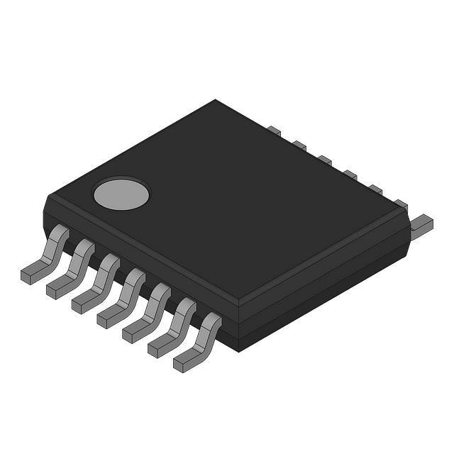


 工商网监
湘ICP备2023018690号
工商网监
湘ICP备2023018690号