�������� ������ � ���
���� ���
��
���
�
���� ������ �����
�� �����
�����
�������� ��� ���
����
����
�
�
������������
� ���������� ���� ±���� ������
SLAS262C − OCTOBER 2000 − REVISED MAY 2003
D 14-Bit Resolution for TLC3574/78, 12-Bit for
D
D
D
D
D
D
D
D
D
D
D
D
D
D
D
TLC2574/2578
Maximum Throughput 200-KSPS
Multiple Analog Inputs:
− 8 Single-Ended Channels for
TLC3578/2578
− 4 Single-Ended Channels for
TLC3574/2574
Analog Input Range: ±10 V
Pseudodifferential Analog Inputs
SPI/DSP-Compatible Serial Interfaces With
SCLK up to 25-MHz
Built-In Conversion Clock and 8x FIFO
Single 5-V Analog Supply; 3-/5-V Digital
Supply
Low-Power
− 5.8 mA in Normal Operation
− 20 µA in Power Down
Programmable Autochannel Sweep and
Repeat
Hardware-Controlled, Programmable
Sampling Period
Hardware Default Configuration
INL: TLC3574/78: ±1 LSB;
TLC2574/78: ±0.5 LSB
DNL: TLC3574/78: ±0.5 LSB;
TLC2574/78: ±0.5 LSB
SINAD: TLC3574/78: 79 dB;
TLC2574/78: 72 dB
THD: TLC3574/78: −82 dB;
TLC2574/78: −82 dB
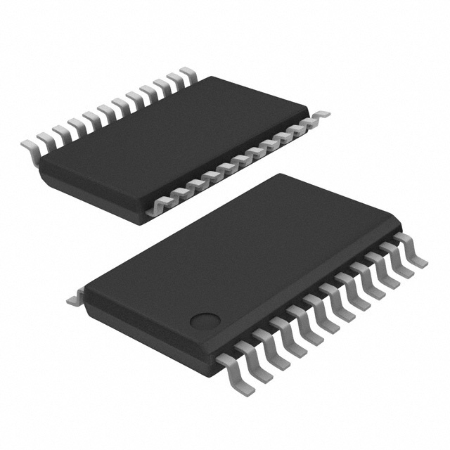
TLC3578, TLC2578
DW OR PW PACKAGE
(TOP VIEW)
SCLK
FS
SDI
EOC/INT
SDO
DGND
DVDD
CS
A0
A1
A2
A3
1
2
3
4
5
6
7
8
9
10
11
12
24
23
22
21
20
19
18
17
16
15
14
13
CSTART
AVDD
AGND
COMP
REFM
REFP
AGND
AVDD
A7
A6
A5
A4
TLC3574, TLC2574
DW, N, OR PW PACKAGE
(TOP VIEW)
SCLK
FS
SDI
EOC/INT
SDO
DGND
DVDD
CS
A0
A1
1
2
3
4
5
6
7
8
9
10
20
19
18
17
16
15
14
13
12
11
CSTART
AVDD
AGND
COMP
REFM
REFP
AGND
AVDD
A3
A2
description
The TLC3574, TLC3578, TLC2574, and TLC2578 are a family of high-performance, low-power, CMOS
analog-to-digital converters (ADC). TLC3574/78 is a 14-bit ADC; TLC2574/78 is a 12-bit ADC. All parts operate
from single 5-V analog power supply and 3-V to 5-V digital supply. The serial interface consists of four digital
input [chip select (CS), frame sync (FS), serial input-output clock (SCLK), serial data input (SDI)], and a 3-state
serial data output (SDO). CS (works as SS, slave select), SDI, SDO and SCLK form an SPI interface. FS, SDI,
SDO, and SCLK form DSP interface. The frame sync signal (FS) indicates the start of a serial data frame being
transferred. When multiple converters connect to one serial port of a DSP, CS works as the chip select to allow
the host DSP to access the individual converter. CS can be tied to ground if only one converter is used. FS must
be tied to DVDD if it is not used (such as in an SPI interface). When SDI is tied to DVDD, the device is set in
hardware default mode after power on and no software configuration is required. In the simplest case, only three
wires (SDO, SCLK, and CS or FS) are needed to interface with the host.
Please be aware that an important notice concerning availability, standard warranty, and use in critical applications of
Texas Instruments semiconductor products and disclaimers thereto appears at the end of this data sheet.
Copyright 2000 − 2003, Texas Instruments Incorporated
���������� �
�
�!"#$%&'�#! �( )*$$+!' &( #" ,*-.�)&'�#! /&'+0
�$#/*)'( )#!"#$% '# (,+)�"�)&'�#!( ,+$ '1+ '+$%( #" �+2&( �!('$*%+!'(
('&!/&$/ 3&$$&!'40 �$#/*)'�#! ,$#)+((�!5 /#+( !#' !+)+((&$�.4 �!).*/+
'+('�!5 #" &.. ,&$&%+'+$(0
WWW.TI.COM
1
��������� ������ � ���
���� ���
��
���
�
���� ������ �����
�� �����
�����
�������� ��� ���
����
����
�
�
������������
� ���������� ���� ±���� ������
SLAS262C − OCTOBER 2000 − REVISED MAY 2003
description (continued)
In addition to being a high-speed ADC with versatile control capability, these devices have an on-chip analog
multiplexer (MUX) that can select any analog input or one of three self-test voltages. The sample-and-hold
function is automatically started after the fourth SCLK (normal sampling) or can be controlled by a special pin,
CSTART, to extend the sampling period (extended sampling). The normal sampling period can also be
programmed as short sampling (12 SCLKs) or long sampling (44 SCLKs) to accommodate the faster SCLK
operation popular among high-performance signal processors. The TLC3574/78 and TLC2574/78 are
designed to operate with low-power consumption. The power saving feature is further enhanced with
autopower-down mode and programmable conversion speeds. The conversion clock (internal OSC) is built in.
The converter can also use an external SCLK as the conversion clock for maximum flexibility. The TLC3574/78
and TLC2574/78 are specified with bipolar input and a full scale range of ±10 V.
AVAILABLE OPTIONS
PACKAGED DEVICES
TA
20-TSSOP
(PW)
−40°C to 85°C
20-SOIC
(DW)
20-PDIP
(N)
24-SOIC
(DW)
24-TSSOP
(PW)
TLC2574IPW
TLC2574IDW
TLC2574IN
TLC2578IDW
TLC2578IPW
TLC3574IPW
TLC3574IDW
TLC3574IN
TLC3578IDW
TLC3578IPW
functional block diagram
DVDD
AVDD
REFP
COMP
REFM
X8† X4‡
A0 A0
A1 A1
A2 A2
A3 A3
X
A4
X
A5
X
A6
X
A7
SAR
ADC
Analog
MUX
Signal
Scaling
FIFO
X8
OSC
SDO
Conversion
Clock
Command
Decode
CFR
SDI
CMR (4 MSBs)
SCLK
CS
FS
4-Bit
Counter
Control
Logic
EOC/INT
CSTART
DGND AGND
† TLC3578, TLC2578
‡ TLC3574, TLC2574
NOTE: 4-Bit counter counts the CLOCK, SCLK. The CLOCK is gated in by CS falling edge if CS initiates the conversion operation cycle, or gated
in by the rising edge of FS if FS initiates the operation cycle. SCLK is disabled for serial interface when CS is high.
2
WWW.TI.COM
��������� ������ � ���
���� ���
��
���
�
���� ������ �����
�� �����
�����
�������� ��� ���
����
����
�
�
������������
� ���������� ���� ±���� ������
SLAS262C − OCTOBER 2000 − REVISED MAY 2003
equivalent input circuit
VDD
REFP
Bipolar Signal Scaling
MUX
3.94 kΩ
Digital Input
1.5 kΩ
9.9 kΩ
Ain
Ron
C(sample)= 30 pF
6.6 kΩ
Equivalent Digital Input Circuit
REFM
Diode Turn on Voltage: 35 V
Equivalent Analog Input Circuit
Terminal Functions
TERMINAL
NO.
NAME
I/O
DESCRIPTION
9
10
11
12
13
14
15
16
I
Analog signal inputs. Analog input signals applied to these terminals are internally multiplexed. The
driving source impedance should be less than or equal to 25 Ω for normal sampling. For larger
source impedance, use the external hardware conversion start signal CSTART (the low time of
CSTART controls the sampling period) or reduce the frequency of SCLK to increase the sampling
time.
14, 18
18, 22
I
Analog ground return for the internal circuitry. Unless otherwise noted, all analog voltage
measurements are with respect to AGND.
13, 19
17, 23
I
Analog supply voltage
17
21
I
Internal compensation pin. Install compensation capacitors 0.1 µF between this pin and AGND.
8
8
I
Chip select. When CS is high, SDO is in high-impedance state, SDI is ignored, and SCLK is
disabled to clock data, but works as conversion clock source if programmed. The falling edge of
CS input resets the internal 4-bit counter, enables SDI and SCLK, and removes SDO from
high-impedance state.
TLC3574
TLC2574
TLC3578
TLC2578
9
10
11
12
AGND
AVDD
COMP
A0
A1
A2
A3
A0
A1
A2
A3
A4
A5
A6
A7
CS
If FS is high at CS falling edge, CS falling edge initiates the operation cycle. CS works as slave
select (SS) to provide an SPI interface.
If FS is low at CS falling edge, FS rising edge initiates the operation cycle. CS can be used as chip
select to allow host to access the individual converter.
CSTART
20
24
I
External sampling trigger signal, which initiates the sampling from a selected analog input channel
when the device works in extended sampling mode (asynchronous sampling). A high-to-low
transition starts the sampling of the analog input signal. A low-to-high transition puts the S/H in hold
mode and starts the conversion. The low time of the CSTART signal controls the sampling period.
CSTART signal must stay low long enough for proper sampling. CSTART must stay high long
enough after the low-to-high transition for the conversion to finish maturely. The activation of
CSTART is independent of SCLK and the level of CS and FS. However, the first CSTART cannot
be issued before the rising edge of the eleventh SCLK. Tie this pin to DVDD if not used.
DGND
6
6
I
Digital ground return for the internal circuitry
DVDD
7
7
I
Digital supply voltage
WWW.TI.COM
3
��������� ������ � ���
���� ���
��
���
�
���� ������ �����
�� �����
�����
�������� ��� ���
����
����
�
�
������������
� ���������� ���� ±���� ������
SLAS262C − OCTOBER 2000 − REVISED MAY 2003
Terminal Functions (Continued)
TERMINAL
NO.
I/O
NAME
TLC3574
TLC2574
TLC3578
TLC2578
EOC(INT)
4
4
O
DESCRIPTION
End of conversion (EOC) or interrupt to host processor (INT)
EOC: used in conversion mode 00 only. EOC goes from high to low at the end of the sampling and
remains low until the conversion is complete and data is ready.
INT: Interrupt to the host processor. The falling edge of INT indicates data is ready for output. INT
is cleared by the following CS↓, FS↑, or CSTART↓.
FS
2
2
I
Frame sync input from DSP. The rising edge of FS indicates the start of a serial data frame being
transferred (coming into or being sent out of the device). If FS is low at the falling edge of CS, the
rising edge of FS initiates the operation cycle, resets the internal 4-bit counter, and enables SDI,
SDO, and SCLK. Tie this pin to DVDD if FS is not used to initiate the operation cycle.
REFM
16
20
I
External low reference input. Connect REFM to AGND.
REFP
15
19
I
External positive reference input. The range of maximum input voltage is determined by the
difference between the voltage applied to this terminal and to the REFM terminal. Always install
decoupling capacitors (10 µF in parallel with 0.1 µF) between REFP and REFM.
SCLK
1
1
I
Serial clock input from the host processor to clock in the input from SDI and clock out the output
via SDO. It can also be used as the conversion clock source when the external conversion clock
is selected (see Table 2). When CS is low, SCLK is enabled. When CS is high, SCLK is disabled
for the data transfer, but can still work as the conversion clock source.
SDI
3
3
I
Serial data input. The first 4 MSBs, ID[15:12], are decoded as one 4-bit command. All trailing bits,
except for the WRITE CFR command, are filled with zeros. The WRITE CFR command requires
additional 12-bit data. The MSB of input data, ID(15), is latched at the first falling edge of SCLK
following FS falling edge if FS starts the operation, or latched at the falling edge of first SCLK
following CS falling edge when CS initiates the operation.
The remaining input data (if any) is shifted in on the rising edge of SCLK and latched on the falling
edge of SCLK. The input via SDI is ignored after the 4-bit counter counts to 16 (clock edges) or a
low-to-high transition of CS, whichever happens first. Refer to the timing specification for the timing
requirements. Tie SDI to DVDD if using hardware default mode (refer to Device Initialization).
SDO
5
5
O
The 3-state serial output for the A/D conversion result. All data bits are shifted out through SDO.
SDO is in the high-impedance state when CS is high. SDO is released after a CS falling edge. The
output format is MSB (OD15) first.
When FS initiates the operation, the MSB of output via SDO, OD(15), is valid before the first falling
edge of SCLK following the falling edge of FS.
When CS initiates the operation, the MSB, OD(15), is valid before the first falling edge of SCLK
following the CS falling edge.
The remaining data bits (if any) are shifted out on the rising edge of SCLK and are valid before the
falling edge of SCLK. Refer to the timing specification for the details.
In select/conversion operation, the first 14 bits (for TLC3574/78) or the first 12 bits (for TLC2574/78)
are the results from the previous conversion (data). In a READ FIFO operation, this data is from
FIFO. In both cases, the last two bits (for TLC3574/78) or the last four bits (for TLC2574/78) are
don’t care.
In a WRITE operation, the output from SDO must be ignored.
SDO goes into high-impedance state at the 16th falling edge of SCLK after the operation cycle is
initiated. SDO is in high-impedance state during conversions in modes 01, 10, and 11.
4
WWW.TI.COM
��������� ������ � ���
���� ���
��
���
�
���� ������ �����
�� �����
�����
�������� ��� ���
����
����
�
�
������������
� ���������� ���� ±���� ������
SLAS262C − OCTOBER 2000 − REVISED MAY 2003
absolute maximum ratings over operating free-air temperature (unless otherwise noted)†
Supply voltage, GND to AVDD and DVDD . . . . . . . . . . . . . . . . . . . . . . . . . . . . . . . . . . . . . . . . . . . . −0.3 V to 6.5 V
Analog input voltage range . . . . . . . . . . . . . . . . . . . . . . . . . . . . . . . . . . . . . . . . . . . . . . . . . . . . . . . . . . −17 V to 17 V
Analog input current . . . . . . . . . . . . . . . . . . . . . . . . . . . . . . . . . . . . . . . . . . . . . . . . . . . . . . . . . . . . . . . . 100 mA MAX
Reference input voltage . . . . . . . . . . . . . . . . . . . . . . . . . . . . . . . . . . . . . . . . . . . . . . . . . . . . . . . . . . . . AVDD + 0.3 V
Digital input voltage range . . . . . . . . . . . . . . . . . . . . . . . . . . . . . . . . . . . . . . . . . . . . . . . . . −0.3 V to DVDD + 0.3 V
Operating virtual junction temperature range, TJ . . . . . . . . . . . . . . . . . . . . . . . . . . . . . . . . . . . . −40°C to 150°C
Operating free-air temperature range, TA . . . . . . . . . . . . . . . . . . . . . . . . . . . . . . . . . . . . . . . . . . . . −40°C to 85°C
Storage temperature range, Tstg . . . . . . . . . . . . . . . . . . . . . . . . . . . . . . . . . . . . . . . . . . . . . . . . . . . −65°C to 150°C
Lead temperature 1,6 mm (1.16 inch) from case for 10 seconds . . . . . . . . . . . . . . . . . . . . . . . . . . . . . . . 260°C
† Stresses beyond those listed under “absolute maximum ratings” may cause permanent damage to the device. These are stress ratings only, and
functional operation of the device at these or any other conditions beyond those indicated under electrical characteristics and timing
characteristics is not implied. Exposure to absolute-maximum-rated conditions for extended periods may affect device reliability.
general electrical characteristics over recommended operating free-air temperature range,
single-ended input, normal long sampling, 200 KSPS, AVDD = 5 V, VREFP = 4 V, VREFM = 0 V,
SCLK frequency = 25 MHz, fixed channel at CONV mode 00, analog input signal source resistance
= 25 Ω (unless otherwise noted)
PARAMETER
TEST CONDITIONS
MIN
TYP†
MAX UNIT
Digital Input
VIH
High-level digital input voltage
VIL
Low-level digital input voltage
IIH
IIL
High-level digital input current
Low-level digital input current
DVDD = 5 V
3.8
DVDD = 3 V
2.1
V
DVDD = 5 V
0.8
DVDD = 3 V
0.6
VI = DVDD
VI = DGND
0.005
−2.5
Input capacitance
2.5
µA
µA
−0.005
20
V
25
pF
Digital Output
VOH
VOL
IOZ
High-level digital output at 30 pF load
Io = −0.2 mA
4.2
DVDD = 3 V
2.4
V
DVDD = 5 V
Io = 0.8 mA
Io = 50 µA
0.4
DVDD = 3 V
Io = 0.8 mA
Io = 50 µA
0.4
Low-level digital output at 30 pF load
VO = DVDD
VO = DGND
Off-state output current
(high-impedance state)
DVDD = 5 V
0.1
V
0.1
0.02
CS = DVDD
1
µA
−1
0.02
4.75
5
5.5
V
2.7
5
5.5
V
4.2
5
1.6
2.0
Power Supply
AVDD
DVDD
ICC
Supply voltage
Power supply current
ICC
(autopwrdn):
AVDD current
AlCC
DVDD current
DlCC
Autopower-down power supply
current
Operating temperature
† All typical values are at TA = 25°C.
Conversion clock is internal OSC,
AVDD = 5.5 V − 4.5 V, CS = DGND,
Excluding bipolar input biasing current
For all digital inputs = DVDD or DGND,
AVDD = 5.5 V, Excluding bipolar input
biasing current, external reference
mA
SCLK OFF
20
SCLK ON
175
−40
WWW.TI.COM
230
85
µA
°C
5
��������� ������ � ���
���� ���
��
���
�
���� ������ �����
�� �����
�����
�������� ��� ���
����
����
�
�
������������
� ���������� ���� ±���� ������
SLAS262C − OCTOBER 2000 − REVISED MAY 2003
general electrical characteristics over recommended operating free-air temperature range, singleended input, normal long sampling, 200 KSPS, AVDD = 5 V, VREFP = 4 V, VREFM = 0 V,
SCLK frequency = 25 MHz, fixed channel at CONV mode 00, analog input signal source
resistance = 25 Ω (unless otherwise noted)
TLC3574/78 and TLC2574/78
PARAMETER
TEST CONDITIONS
MIN
Resolution
TYP†
MAX
14
UNIT
bits
Analog Input
Voltage range
−10
Selected channel at 10 V
Selected analog input channel bias current
10
0.8
Selected channel at –10 V
−1.6
V
1.6
mA
−1.2
Impedance
10
kΩ
Capacitance
30
pF
Reference
VREFP
VREFM
Positive reference voltage
Negative reference voltage
Input impedance
3.96
4
0
AGND
No conversion (AVDD = 5V, CS= DVDD,
SCLK=DGND)
100
Normal long sampling (AVDD = 5V, CS=DGND,
SCLK = 25 MHz, External conversion clock)
8.3
Internal oscillation frequency
Normal long sampling (AVDD = 5 V, CS = DGND,
External conversion clock, SCLK = 25 MHz,
VREF = 5 V)
DVDD = 2.7 V – 5.5 V
Internal OSC, 6.5 MHz minimum
t(conv)
Conversion time
Conversion clock is external source,
SCLK = 25 MHz (see Note 1)
Acquisition time
Normal short sampling
Throughput rate (see Note 2)
Normal long sampling, fixed channel
in mode 00 or 01
V
12.5
0.4
kΩ
1.5
µA
0.6
mA
6.5
MHz
TLC3574/78
2.785
TLC2574/78
2.015
TLC3574/78
2.895
TLC2574/78
2.095
1.2
200
V
MΩ
No conversion (AVDD = 5 V,
SCLK = DGND, CS = DVDD)
Reference current
4.04
µS
S
µS
KSPS
† All typical values are at TA = 25°C.
NOTES: 1. Conversion time t(conv) is (18 × 4 × SCLK) + 15 ns for TLC3574/78. Conversion time is (13 × 4 × SCLK) + 15 ns for TLC2574/78.
2. This is for a fixed channel in conversion mode 00 or 01. When switching the channels, additional multiplexer setting time is required
to overcome the memory effect of the charge redistribution DAC.
6
WWW.TI.COM
��������� ������ � ���
���� ���
��
���
�
���� ������ �����
�� �����
�����
�������� ��� ���
����
����
�
�
������������
� ���������� ���� ±���� ������
SLAS262C − OCTOBER 2000 − REVISED MAY 2003
AC/DC performance over recommended operating free-air temperature range, single-ended input,
normal long sampling, 200 KSPS, AVDD = 5 V, VREFP = 4 V, VREFM = 0 V, SCLK frequency = 25 MHz,
fixed channel at CONV mode 00, analog input signal source resistance = 25 Ω (unless otherwise
noted)
TLC3574/78 DW and PW package device AC/DC performance
MIN
TYP†
MAX
UNIT
See Note 3
−1.5
±1
1.5
LSB
PARAMETER
TEST CONDITIONS
DC Accuracy—Normal Long Sampling
EL
ED
Integral linearity error
−1
±0.5
1
LSB
EO
EFS(+)
Bipolar zero error
See Note 4
−0.30
±0.08
0.36
%FS
Positive full scale error
Differential linearity error
See Note 4
−0.55
±0.04
0.61
%FS
EFS(−)
Negative full scale error
DC Accuracy—Normal Short Sampling
See Note 4
−0.30
±0.13
0.79
%FS
EL
ED
Integral linearity error
See Note 3
EO
EFS(+)
Bipolar zero error
Positive full scale error
±1
LSB
±0.5
LSB
See Note 4
±0.08
%FS
See Note 4
±0.04
%FS
EFS(−)
Negative full scale error
See Note 4
AC Accuracy (see Note 3)—Normal Long Sampling
±0.13
%FS
Differential linearity error
SINAD
Signal-to-noise ratio + distortion
fi = 20 kHz
fi = 100 kHz
THD
Total harmonic distortion
fi = 20 kHz
fi = 100 kHz
SNR
Signal-to-noise ratio
fi = 20 kHz
fi = 100 kHz
78
ENOB
Effective number of bits
fi = 20 kHz
fi = 100 kHz
12.3
SFDR
Spurious free dynamic range
fi = 20 kHz
fi = 100 kHz
78
Channel-to-channel isolation
Fixed channel in conversion mode 00, fi = 35 kHz,
See Notes 2 and 5
Analog input bandwidth
76
79
dB
75
−82
−78
80
78
12.8
12.2
84
79
−77
dB
dB
Bits
dB
81
dB
Full power bandwidth, −3 dB
1
MHz
Full power bandwidth, −1 dB
700
kHz
† All typical values are at TA = 25°C.
NOTES: 2. This is for a fixed channel in conversion mode 00 or 01. When switching the channels, additional multiplexer setting time is required
to overcome the memory effect of the charge redistribution DAC.
3. Linear error is the maximum deviation from the best fit straight line through the A/D transfer characteristics.
4. Bipolar zero error is the difference between 10000000000000 and the converted output for zero input voltage; positive full-scale error
is the difference between 11111111111111 and the converted output for positive full-scale input voltage (10 V); negative full-scale
error is the difference between 00000000000000 and the converted output for negative full-scale input voltage (−10 V).
5. It is measured by applying a full-scale of 35 kHz signal to other channels and determining how much the signal is attenuated in the
channel of interest. The converter samples this examined channel continuously. The channel-to-channel isolation is degraded if the
converter samples different channels alternately.
WWW.TI.COM
7
��������� ������ � ���
���� ���
��
���
�
���� ������ �����
�� �����
�����
�������� ��� ���
����
����
�
�
������������
� ���������� ���� ±���� ������
SLAS262C − OCTOBER 2000 − REVISED MAY 2003
TLC3574/78 DW and PW package device AC/DC performance (continued)
PARAMETER
TEST CONDITIONS
MIN
TYP†
MAX
UNIT
AC Accuracy—Normal Short Sampling
SINAD
Signal-to-noise ratio + distortion
fi = 20 kHz
fi = 100 kHz
79
THD
Total harmonic distortion
fi = 20 kHz
fi = 100 kHz
−82
SNR
Signal-to-noise ratio
fi = 20 kHz
fi = 100 kHz
80
ENOB
Effective number of bits
fi = 20 kHz
fi = 100 kHz
12.8
SFDR
Spurious free dynamic range
fi = 20 kHz
fi = 100 kHz
84
Channel-to-channel isolation
Fixed channel in conversion mode 00, fi= 35 kHz,
See Notes 2 and 5
Analog input bandwidth
75
−78
78
12.2
79
dB
dB
dB
Bits
dB
81
dB
Full power bandwidth, −3 dB
1
MHz
Full power bandwidth, −1 dB
700
kHz
† All typical values are at TA = 25°C.
NOTES: 2. This is for a fixed channel in conversion mode 00 or 01. When switching the channels, additional multiplexer setting time is required
to overcome the memory effect of the charge redistribution DAC.
5. It is measured by applying a full-scale of 35 kHz signal to other channels and determining how much the signal is attenuated in the
channel of interest. The converter samples this examined channel continuously. The channel-to-channel isolation is degraded if the
converter samples different channels alternately.
8
WWW.TI.COM
��������� ������ � ���
���� ���
��
���
�
���� ������ �����
�� �����
�����
�������� ��� ���
����
����
�
�
������������
� ���������� ���� ±���� ������
SLAS262C − OCTOBER 2000 − REVISED MAY 2003
TLC3574I N package device AC/DC performance
PARAMETER
TEST CONDITIONS
TYP†
MAX
UNIT
−1.5
±1
1.5
LSB
−1
±0.8
1.5
LSB
MIN
DC Accuracy—Normal Long Sampling
EL
ED
Integral linearity error
See Note 3
EO
EFS(+)
Bipolar zero error
See Note 4
−0.30
±0.08
0.36
%FS
Positive full scale error
Differential linearity error
See Note 4
−0.55
±0.04
0.61
%FS
EFS(−)
Negative full scale error
DC Accuracy—Normal Short Sampling
See Note 4
−0.30
±0.13
0.79
%FS
EL
ED
Integral linearity error
See Note 3
±1.8
±0.8
LSB
EO
EFS(+)
Bipolar zero error
See Note 4
±0.08
%FS
Positive full-scale error
See Note 4
±0.04
%FS
EFS(−)
Negative full-scale error
See Note 4
AC Accuracy (see Note 3)—Normal Long Sampling
±0.13
%FS
Differential linearity error
SINAD
Signal-to-noise ratio + distortion
fi = 20 kHz
fi = 100 kHz
THD
Total harmonic distortion
fi = 20 kHz
fi = 100 kHz
SNR
Signal-to-noise ratio
fi = 20 kHz
fi = 100 kHz
78
ENOB
Effective number of bits
fi = 20 kHz
fi = 100 kHz
12.2
SFDR
Spurious free dynamic range
fi = 20 kHz
fi = 100 kHz
78
Channel-to-channel isolation
Fixed channel in conversion mode 00, fi = 35 kHz,
See Notes 2 and 5
Analog input bandwidth
75
LSB
78
dB
75
−82
−75
80
76
12.7
12.2
83
75
−77
dB
dB
Bits
dB
81
dB
Full power bandwidth, −3 dB
1
MHz
Full power bandwidth, −1 dB
700
kHz
† All typical values are at TA = 25°C.
NOTES: 2. This is for a fixed channel in conversion mode 00 or 01. When switching the channels, additional multiplexer setting time is required
to overcome the memory effect of the charge redistribution DAC.
3. Linear error is the maximum deviation from the best fit straight line through the A/D transfer characteristics.
4. Bipolar zero error is the difference between 10000000000000 and the converted output for zero input voltage; positive full-scale error
is the difference between 11111111111111 and the converted output for positive full-scale input voltage (10 V); negative full-scale
error is the difference between 00000000000000 and the converted output for negative full-scale input voltage (−10 V).
5. It is measured by applying a full-scale of 35 kHz signal to other channels and determining how much the signal is attenuated in the
channel of interest. The converter samples this examined channel continuously. The channel-to-channel isolation is degraded if the
converter samples different channels alternately.
WWW.TI.COM
9
��������� ������ � ���
���� ���
��
���
�
���� ������ �����
�� �����
�����
�������� ��� ���
����
����
�
�
������������
� ���������� ���� ±���� ������
SLAS262C − OCTOBER 2000 − REVISED MAY 2003
TLC3574I N package device AC/DC performance (continued)
PARAMETER
TEST CONDITIONS
MIN
TYP†
MAX
UNIT
AC Accuracy—Normal Short Sampling
SINAD
Signal-to-noise ratio + distortion
fi = 20 kHz
fi = 100 kHz
76
THD
Total harmonic distortion
fi = 20 kHz
fi = 100 kHz
−81
SNR
Signal-to-noise ratio
fi = 20 kHz
fi = 100 kHz
78
ENOB
Effective number of bits
fi = 20 kHz
fi = 100 kHz
12.3
SFDR
Spurious free dynamic range
fi = 20 kHz
fi = 100 kHz
83
Channel-to-channel isolation
Fixed channel in conversion mode 00, fi= 35 kHz,
See Notes 2 and 5
Analog input bandwidth
70
−74
75
11.3
75
dB
dB
dB
Bits
dB
81
dB
Full power bandwidth, −3 dB
1
MHz
Full power bandwidth, −1 dB
700
kHz
† All typical values are at TA = 25°C.
NOTES: 2. This is for a fixed channel in conversion mode 00 or 01. When switching the channels, additional multiplexer setting time is required
to overcome the memory effect of the charge redistribution DAC.
5. It is measured by applying a full-scale of 35 kHz signal to other channels and determining how much the signal is attenuated in the
channel of interest. The converter samples this examined channel continuously. The channel-to-channel isolation is degraded if the
converter samples different channels alternately.
10
WWW.TI.COM
��������� ������ � ���
���� ���
��
���
�
���� ������ �����
�� �����
�����
�������� ��� ���
����
����
�
�
������������
� ���������� ���� ±���� ������
SLAS262C − OCTOBER 2000 − REVISED MAY 2003
TLC2574/78 DW and PW package devices AC/DC performance
MIN
TYP†
MAX
UNIT
See Note 6
−1
±0.5
1
LSB
PARAMETER
TEST CONDITIONS
DC Accuracy
EL
ED
Integral linearity error
−1
±0.5
1
LSB
EO
EFS(+)
Bipolar zero error
See Note 7
−0.30
±0.08
0.36
%FS
Positive full scale error
See Note 7
−0.55
±0.04
0.61
%FS
See Note 7
−0.30
±0.13
0.79
%FS
70
72
Differential linearity error
EFS(−)
Negative full scale error
AC Accuracy
SINAD
Signal-to-noise ratio + distortion
THD
Total harmonic distortion
SNR
Signal-to-noise ratio
ENOB
Effective number of bits
SFDR
Spurious free dynamic range
Analog input bandwidth
Channel-to-channel Isolation
fi = 20 kHz
fi = 100 kHz
fi = 20 kHz
dB
70
−82
fi = 100 kHz
fi= 20 kHz
−80
71
fi = 100 kHz
fi = 20 kHz
11.3
dB
11.7
11.3
78
dB
72
71
fi = 100 kHz
fi = 20 kHz
−76
Bits
83
dB
fi = 100 kHz
Full power bandwidth, −3 dB
80
1
MHz
Full power bandwidth, −1 dB
700
kHz
81
dB
Fixed channel in conversion mode 00, fi = 35 kHz,
See Note 8
† All typical values are at TA = 25°C.
NOTES: 6. Linear error is the maximum deviation from the best fit straight line through the A/D transfer characteristics.
7. Bipolar zero error is the difference between 100000000000 and the converted output for zero input voltage; positive full-scale error
is the difference between 111111111111 and the converted output for positive full-scale input voltage (10 V); negative full-scale error
is the difference between 000000000000 and the converted output for negative full-scale input voltage (−10 V).
8. It is measured by applying a full-scale of 35 kHz signal to other channels and determining how much the signal is attenuated in the
channel of interest. The converter samples this examined channel continuously. The channel-to-channel isolation is degraded if the
converter samples different channels alternately.
WWW.TI.COM
11
��������� ������ � ���
���� ���
��
���
�
���� ������ �����
�� �����
�����
�������� ��� ���
����
����
�
�
������������
� ���������� ���� ±���� ������
SLAS262C − OCTOBER 2000 − REVISED MAY 2003
TLC2574I N package device AC/DC performance
MIN
TYP†
MAX
UNIT
see Note 6
−1
±0.7
1
LSB
PARAMETER
TEST CONDITIONS
DC Accuracy
EL
ED
Integral linearity error
−1
±0.7
1
LSB
EO
EFS(+)
Bipolar zero error
see Note 7
−0.30
±0.08
0.36
%FS
Positive full-scale error
see Note 7
−0.55
±0.04
0.61
%FS
see Note 7
−0.30
±0.13
0.79
%FS
70
72
Differential linearity error
EFS(−)
Negative full-scale error
AC Accuracy
SINAD
Signal-to-noise + distortion
THD
Total harmonic distortion
SNR
Signal-to-noise ratio
ENOB
Effective number of bits
SFDR
Spurious free dynamic range
Analog input bandwidth
Channel-to-channel Isolation
fi = 20 kHz
fi = 100 kHz
fi = 20 kHz
dB
70
−82
fi = 100 kHz
fi= 20 kHz
−75
70
fi = 100 kHz
fi = 20 kHz
11.3
dB
11.7
11.3
77
dB
72
71
fi = 100 kHz
fi = 20 kHz
−76
Bits
83
dB
fi = 100 kHz
Full power bandwidth, −3 dB
75
1
MHz
Full power bandwidth, −1 dB
700
kHz
81
dB
Fixed channel in conversion mode 00, fi = 35 kHz,
See Note 8
† All typical values are at TA = 25°C.
NOTES: 6. Linear error is the maximum deviation from the best fit straight line through the A/D transfer characteristics.
7. Bipolar zero error is the difference between 100000000000 and the converted output for zero input voltage; positive full-scale error
is the difference between 111111111111 and the converted output for positive full-scale input voltage (10 V); negative full-scale error
is the difference between 000000000000 and the converted output for negative full-scale input voltage (−10 V).
8. It is measured by applying a full-scale of 35 kHz signal to other channels and determining how much the signal is attenuated in the
channel of interest. The converter samples this examined channel continuously. The channel-to-channel isolation is degraded if the
converter samples different channels alternately.
12
WWW.TI.COM
��������� ������ � ���
���� ���
��
���
�
���� ������ �����
�� �����
�����
�������� ��� ���
����
����
�
�
������������
� ���������� ���� ±���� ������
SLAS262C − OCTOBER 2000 − REVISED MAY 2003
timing requirements over recommended operating free-air temperature range, AVDD = 5 V,
DVDD = 5 V, VREFP = 4 V, VREFM = 0 V, SCLK frequency = 25 MHz (unless otherwise noted)
SCLK, SDI, SDO, EOC and INT
PARAMETERS
tc(1)
Cycle time of SCLK, 25 pF load (see Note 10)
tw(1)
Pulse width of SCLK High, at 25-pF load
MIN
DVDD = 2.7 V
DVDD = 5 V
TYP
MAX
100
UNIT
ns
40
40%
60%
DVDD = 5 V
DVDD = 2.7 V
6
tc(1)
tr(1)
Rise time for INT and EOC, at 10-pF load
tf(1)
Fall time for INT and EOC, at 10-pF load
tsu(1)
th(1)
DVDD = 5 V
DVDD = 2.7 V
Setup time, new SDI valid (reaches 90% final level) before the falling edge of SCLK, at 25-pF load
6
−
ns
Hold time, old SDI hold (reaches 10% of old data level) after falling edge of SCLK, at 25-pF load
0
−
ns
0
10
0
23
td(1)
Delay time, new SDO valid (reaches 90% of final level) after SCLK rising edge, at 10-pF
load (see Note 11)
10
6
10
DVDD = 5 V
DVDD = 2.7 V
ns
ns
ns
th(2)
td(2)
Hold time, old SDO hold (reaches 10% of old data level) after SCLK rising edge, at 10-pF load
0
−
ns
Delay time, delay from the falling edge of 16th SCLK to EOC falling edge, normal sampling, at 10-pF load
0
6
ns
td(3)
Delay time, delay from the falling edge of 16th SCLK to INT falling edge, at 10-pF load (see Notes 11 and 12)
t(conv)
t(conv)+6
ns
NOTES: 9. The minimum pulse width of SCLK high and low is 12.5 ns.
10. Specified by design
11. For normal short sampling, td(3) is the delay from the falling edge of 16th SCLK to the falling edge of INT.
For normal long sampling, td(3) is the delay from the falling edge of 48th SCLK to the falling edge of INT. Conversion time, t(conv),
is equal to 18 × OSC +15 ns (for TLC3574 and TLC3578) or 13 × OSC + 15 ns (for TLC2574 and TLC2578) when using internal
OSC as conversion clock, or 72 × tc(1) + 15 ns (for TLC3574 and TLC3578) or 52 × tc(1) + 15 ns (for TLC2574 and TLC2578) when
external SCLK is conversion clock source.
VIH
90%
50%
10%
CS
VIL
tc(1)
tw(1)
1
SCLK
16
th(1)
tsu(1)
SDI
Don’t Care
ID15 ID1
ID0
Don’t Care
td(1)
th(2)
SDO
Hi-Z
OD15 OD1
Hi-Z
OD0
td(2) †
tr(1)
EOC
tf(1)
OR
td(3) ‡
INT
tf(1)
tr(1)
† For normal long sampling, td(2) is the delay time of EOC low after the falling edge of 48th SCLK.
‡ For normal long sampling, td(3) is the delay time of INT low after the falling edge of 48th SCLK.
−−−−
The dotted line means signal may or may not exist, depending on application. It must be ignored.
Normal sampling mode, CS initiatesthe conversion, FS must be tied to high. When CS is high, SDO is in Hi-Z, all inputs (FS, SCLK,
SDI) are inactive and are ignored.
Figure 1. Critical Timing for SCLK, SDI, SDO, EOC and INT
WWW.TI.COM
13
��������� ������ � ���
���� ���
��
���
�
���� ������ �����
�� �����
�����
�������� ��� ���
����
����
�
�
������������
� ���������� ���� ±���� ������
SLAS262C − OCTOBER 2000 − REVISED MAY 2003
timing requirements over recommended operating free-air temperature range, AVDD = 5 V,
DVDD = 5 V, VREFP = 4 V, VREFM = 0 V, SCLK frequency = 25 MHz (unless otherwise noted) (continued)
CS trigger
PARAMETERS
MIN
TYP
MAX
UNIT
tsu(2)
Setup time, CS falling edge before SCLK rising edge, at 25-pF load
12
ns
td(4)
Delay time, delay time from the falling edge of 16th SCLK to CS rising edge, at 25 pF load
(see Note 12)
5
ns
tw(2)
Pulse width of CS high, at 25-pF load
1
td(5)
Delay time, delay from CS falling edge to MSB of SDO valid (reaches 90%
final level), at 10 pF load
td(6)
Delay time, delay from CS rising edge to SDO 3-state, at 10-pF load
td(7)
Delay time, delay from CS falling edge to INT rising edge, at 10-pF load
DVDD = 5 V
0
DVDD = 2.7 V
tc(1)
0
12
30†
ns
0
6
ns
DVDD = 5 V
0
DVDD = 2.7 V
0
6
†
16
ns
† Specified by design
NOTE 12: For normal short sampling, td(4) is the delay time from the falling edge of 16th SCLK to CS rising edge.
For normal long sampling, td(4) is the delay time from the falling edge of 48th SCLK to CS rising edge.
VIH
VIL
CS
tsu(2)
SCLK
SDI
SDO
td(4)
1
Don’t Care
Hi-Z
tw(2)
16
ID1
ID0
Don’t Care
OD15 OD1
OD0
Hi-Z
ID15
Don’t Care
td(6)
td(5)
OD15
OD7
Hi-Z
EOC
OR
td(7)
INT
−−−−
The dotted line means signal may or may not exist, depending on application. It must be ignored.
Normal sampling mode, CS initiates the conversion, FS must be tied to high. When CS is high, SDO is in Hi-Z, all inputs (FS, SCLK,
SDI) are inactive and are ignored.
Figure 2. Critical Timing for CS Trigger
14
WWW.TI.COM
��������� ������ � ���
���� ���
��
���
�
���� ������ �����
�� �����
�����
�������� ��� ���
����
����
�
�
������������
� ���������� ���� ±���� ������
SLAS262C − OCTOBER 2000 − REVISED MAY 2003
timing requirements over recommended operating free-air temperature range, AVDD = 5 V,
DVDD = 5 V, VREFP = 4 V, VREFM = 0 V, SCLK frequency = 25 MHz (unless otherwise noted) (continued)
FS trigger
PARAMETERS
MIN
td(8)
tsu(3)
Delay time, delay from CS falling edge to FS rising edge at 25-pF load
tw(3)
Pulse width of FS high, at 25-pF load
TYP
MAX
tc(1)
0.5×tc(1)+ 5
1.25×tc(1)
0.5
Setup time, FS rising edge before SCLK falling edge at 25-pF load
0.25×tc(1)
0.75×tc(1)
DVDD = 5 V
td(9)
Delay time, delay from FS rising edge to MSB of SDO valid
(reaches 90% final level), at 10-pF load
td(10)
Delay time, delay from FS rising edge to next FS rising edge, at 25-pF load
td(11)
Delay time, delay from FS rising edge to INT rising edge, at
10-pF load
UNIT
tc(1)
ns
ns
26
30†
DVDD = 2.7 V
Required
sampling time +
conversion time
ns
ns
DVDD = 5 V
0
6
DVDD = 2.7 V
0
16†
ns
† Specified by design
VIH
VIL
td(10)
CS
td(8)
tw(3)
FS
tsu(3)
SCLK
SDI
Don’t Care
16
1
ID15 ID1
ID0
Don’t Care
ID15
Don’t Care
td(9)
SDO
Hi-Z
OD15
OD1
OD0
Hi-Z
OD15
Don’t Care
VOH
EOC
OR
td(11)
VOH
INT
−−−−
The dotted line means signal may or may not exist, depending on application. It must be ignored.
Normal sampling mode, FS initiates the conversion, CS can be tied to low. When CS is high, SDO is in Hi-Z, all inputs (FS, SCLK,
SDI) are inactive and are ignored.
Figure 3. Critical Timing for FS Trigger
WWW.TI.COM
15
��������� ������ � ���
���� ���
��
���
�
���� ������ �����
�� �����
�����
�������� ��� ���
����
����
�
�
������������
� ���������� ���� ±���� ������
SLAS262C − OCTOBER 2000 − REVISED MAY 2003
timing requirements over recommended operating free-air temperature range, AVDD = 5 V,
DVDD = 5 V, VREFP = 4 V, VREFM = 0 V, SCLK frequency = 25 MHz (unless otherwise noted) (continued)
CSTART trigger
PARAMETERS
MIN
td(12)
Delay time, delay from CSTART rising edge to EOC falling edge, at 10-pF
load
tw(4)
Pulse width of CSTART low, at 25-pF load (see Note 13)
td(13)
0
TYP
MAX
15
21
UNIT
ns
t(sample_reg)+0.4
µs
Delay time, delay from CSTART rising edge to CSTART falling edge, at 25-pF
load (see Note 13 and 14)
t(conv)+15
ns
td(14)
Delay time, delay from CSTART rising edge to INT falling edge, at 10-pF
load (see Note 13 and 14)
t(conv)+15
td(15)
Delay time, delay from CSTART falling edge to INT rising edge, at 10-pF
load
0
t(conv)+21
ns
6
ns
NOTES: 13. The pulse width of the CSTART must be not less than the required sampling time.
The delay from CSTART rising edge to following CSTART falling edge must be not less than the required conversion time.
The delay from CSTART rising edge to the INT falling edge is equal to the conversion time.
14. The maximum rate of SCLK is 25 MHz for normal long sampling and 10 MHz for normal short sampling.
tw(4)
td(13)
CSTART
t(conv)
td(12)
EOC
td(15)
OR
td(14)
INT
Figure 4. Critical Timing for Extended Sampling (CSTART Trigger)
16
WWW.TI.COM
��������� ������ � ���
���� ���
��
���
�
���� ������ �����
�� �����
�����
�������� ��� ���
����
����
�
�
������������
� ���������� ���� ±���� ������
SLAS262C − OCTOBER 2000 − REVISED MAY 2003
circuit description
converter
The converters include a successive-approximation ADC utilizing a charge redistribution DAC. Figure 5 shows
a simplified block diagram of the ADC. The sampling capacitor acquires the signal on Ain during the sampling
period. When the conversion process starts, the control logic directs the charge redistribution DAC to add and
subtract fixed amounts of charge from the sampling capacitor to bring the comparator into a balanced condition.
When balanced, the conversion is complete and the ADC output code is generated.
Charge
Redistribution
DAC
_
Ain
C(sample)
Control
Logic
+
ADC Code
REFM
Figure 5. Simplified Block Diagram of the Successive-Approximation System
analog input range and internal test voltages
TLC3578 and TLC2578 have 8 analog inputs (TLC3574 and TLC2574 have 4) and three test voltages. The
inputs are selected by the analog multiplexer according to the command entered (see Table 1). The input
multiplexer is a break-before-make type to reduce input-to-input noise injection resulting from channel
switching.
All converters are specified for bipolar input range of ±10 V. The input signal is scaled to 0–4 V at the SAR ADC
input via the bipolar scaling circuit (see the functional block diagram and the equivalent analog input circuit):
–10 V to 0 V, 10 V to 4 V, and 0 V to 2 V.
analog input mode
Two input signal modes can be selected: single-ended input and pseudodifferential input.
Charge
Redistribution
DAC
S1
Ain(+)
_
Ain(−)
+
REFM
Control
Logic
ADC Code
When sampling, S1 is closed and S2 connects to Ain(−).
During conversion, S1 is open and S2 connects to REFM.
Figure 6. Simplified Pseudodifferential Input Circuit
Pseudodifferential input refers to the negative input, Ain(−). Its voltage is limited in magnitude to ±1 V. The input
frequency limit of Ain(−) is the same as the positive input Ain(+). This mode is normally used for ground noise
rejection or dc offset.
WWW.TI.COM
17
��������� ������ � ���
���� ���
��
���
�
���� ������ �����
�� �����
�����
�������� ��� ���
����
����
�
�
������������
� ���������� ���� ±���� ������
SLAS262C − OCTOBER 2000 − REVISED MAY 2003
analog input mode (continued)
When pseudodifferential mode is selected, only two analog input channel pairs are available for the TLC3574
and TLC2574 and four channel pairs for the TLC3578 and TLC2578, because half the inputs are used as the
negative input.
Single Ended
X8† X4‡
A0 A0
A1 A1
A2 A2
A3 A3
X
A4
X
A5
X
A6
X
A7
Pseudodifferential
SAR
ADC
Analog
MUX
X8†
A0(+)
A1(−)
A2(+)
A3(−)
A4(+)
A5(−)
A6(+)
A7(−)
Pair A
Pair B
X4‡
A0(+) Pair A
A1(−)
A2(+) Pair B
A3(−)
Pair C
SAR
ADC
Analog
MUX
Pair D
† TLC3578 and TLC2578
‡ TLC3574 and TLC2574
Figure 7. Pin Assignment of Single-Ended Input vs Pseudodifferential Input
reference voltage
The external reference is applied to the reference-input pins (REFP and REFM). REFM should connect to
analog ground. REFP is 4 V. Install decoupling capacitors (10 µF in parallel with 0.1 µF) between REFP and
REFM, and compensation capacitors (0.1 µF) between COMP and AGND.
ideal conversion characteristics
Bipolar Analog Input Voltage
−9.99756 V
−9.99878 V
VBZS = 0.0 V
−0.61 mV
0.61 mV
1LSB = 1.22 mV
9.99756 V
−9.99939 V
VFS+ = 10 V
18
2s Complement
BTC
01111111111111
Binary
BOB
11111111111111
01111111111110
11111111111110
16383
01111111111101
11111111111101
16382
16381
00000000000001
10000000000001
8193
00000000000000
10000000000000
8192
11111111111111
01111111111111
8191
10000000000010
00000000000010
2
10000000000001
00000000000001
1
10000000000000
00000000000000
0
WWW.TI.COM
Step
Digital Output Code
VFS− = −10 V
��������� ������ � ���
���� ���
��
���
�
���� ������ �����
�� �����
�����
�������� ��� ���
����
����
�
�
������������
� ���������� ���� ±���� ������
SLAS262C − OCTOBER 2000 − REVISED MAY 2003
circuit description (continued)
data format
INPUT DATA FORMAT (BINARY)
MSB
LSB
ID[15:12]
ID[11:0]
Command
Configuration data field or filled with zeros
OUTPUT DATA FORMAT (READ CONVERSION/FIFO)
TLC3574 and TLC3578
TLC2574 and TLC2578
MSB
LSB
MSB
LSB
OD[15:2]
OD[1:0]
OD[15:4]
OD[3:0]
Conversion result
Don’t Care
Conversion result
Don’t Care
14-BIT (TLC3574/78)
12-BIT (TLC2574/78)
Bipolar Input, Offset Binary: (BOB)
Negative full scale code = VFS− = 0000h, Vcode = −10 V
Midscale code = VBZS = 2000h, Vcode = 0 V
Positive full scale code = VFS+ = 3FFFh, Vcode = 10 V − 1 LSB
Bipolar Input, Binary 2s Complement: (BTC)
Negative full scale code = VFS− = 2000 h, Vcode = −10 V
Midscale code = VBZS = 0000h, Vcode = 0 V
Positive full scale code = VFS+ = 1FFFh, Vocde = 10 V − 1 LSB
Bipolar Offset Binary Output: (BOB)
Negative full scale code = 000h, Vcode = −10 V
Midscale code = 800h, Vcode = 0 V
Positive full scale code = FFFh, Vcode = 10 V − 1 LSB
Bipolar Input, Binary 2s Complement: (BTC)
Negative full scale code = 800 h, Vcode = −10 V
Midscale code = 000h, Vcode = 0 V
Positive full scale code = 7FFh, Vocde = 10 V − 1 LSB
operation description
The converter samples the selected analog input signal, then converts the sample into digital output according
to the selected output format. The converter has four digital input pins (SDI, SCLK, CS, and FS) and one digital
output pin (SDO) to communicate with the host device. SDI is a serial data input pin, SDO is a serial data output
pin, and SCLK is a serial clock from host device. This clock is used to clock the serial data transfer. It can also
be used as conversion clock source (see Table 2). CS and FS are used to start the operation. The converter
has a CSTART pin for external hardware sampling and conversion trigger, and INT/EOC for interrupt purpose.
device initialization
After power on, the status of EOC/INT is initially high, and the input data register is set to all zeros. The device
must be initialized before starting conversion. The initialization procedure depends on the working mode. The
first conversion result must be ignored after power on.
Hardware Default Mode: Nonprogrammed mode, default. After power on, two consecutive active cycles
initiated by CS or FS put the device into hardware default mode if SDI is tied to DVDD. Each of these cycles must
last 16 SCLK at least. These cycles initialize the converter and load CFR register with 800h (bipolar offset binary
output code, normal long sampling, internal OSC, single-ended input, one-shot conversion mode, and EOC/INT
pin as INT). No additional software configuration is required.
Software Programmed Mode: Programmed. If the converter needs to be configured, The host must write
A000H into converters first after power on, then performs the WRITE CFR operation to configure the device.
start of operation cycle
Each operation consists of several actions that the converter takes according to the command from the host.
The operation cycle includes three periods: command period, sampling period, and conversion period. In the
command period, the device decodes the command from host. In the sampling period, the device samples the
selected analog signal according to the command. In the conversion period, the sample of the analog signal
is converted to digital format. The operation cycle starts from the command period, which is followed by one
or several sampling and conversion periods (depending on the setting), and finishes at the end of last
conversion period. The operation is initiated by the falling edge of CS or the rising edge of FS.
WWW.TI.COM
19
��������� ������ � ���
���� ���
��
���
�
���� ������ �����
�� �����
�����
�������� ��� ���
����
����
�
�
������������
� ���������� ���� ±���� ������
SLAS262C − OCTOBER 2000 − REVISED MAY 2003
start of operation cycle (continued)
CS initiates the operation: If FS is high at the falling edge of CS, the falling edge of CS initiates the operation.
When CS is high, SDO is in high-impedance state, the signals on SDI are ignored, and SCLK is disabled to clock
the serial data. The falling edge of CS resets the internal 4-bit counter and enables SDO, SDI, and SCLK. The
MSB of the input data via SDI, ID(15), is latched at the first falling edge of SCLK following the falling edge of
CS. The MSB of output data from SDO, OD(15), is valid before this SCLK falling edge. This mode works as an
SPI interface when CS is used as SLAVE SELECT (SS). It also can be used as normal DSP interface if CS
connects to the frame sync output of the host DSP. FS must be tied to high in this mode.
FS initiates the operation: If FS is low at the falling edge of CS, the rising edge of FS initiates the operation.
It resets the internal 4-bit counter, and enables SDI, SDO, and SCLK. The ID(15) is latched at the first falling
edge of SCLK following the falling edge of FS. OD(15) is valid before this falling edge of SCLK. This mode is
used to interface the converter with a serial port of the host DSP. The FS of the device is connected to the frame
sync of the host DSP. When several devices are connected to one DSP serial port, CS is used as chip select
to allow the host DSP to access each device individually. If only one converter is used, CS can be tied to low.
After the initiation, the remaining SDI data bits (if any) are shifted in and the remaining bits of SDO (if any) are
shifted out at the rising edge of SCLK. The input data are latched at the falling edge of SCLK, and the output
data are valid before the falling edge of SCLK. After the 4-bit counter reaches 16, the SDO goes to
high-impedance state. The output data from SDO is the previous conversion result in one shot conversion
mode, or the contents in the top of FIFO when FIFO is used (refer to Figure 20).
command period
After the rising edge of FS (FS triggers the operation) or the falling edge of CS (CS triggers the operation), SDI,
SDO, and SCLK are enabled. The first four SCLK clocks form the command period. The four MSBs of input data,
ID[15:12], are shifted in and decoded. These bits represent one of the 4-bit commands from the host, which
defines the required operation (see Table 1). The four MSB of output, OD[15:12], are also shifted out via SDO
during this period.
The commands are SELECT/CONVERSION, WRITE CFR, FIFO READ, and HARDWARE DEFAULT. The
SELECT/CONVERSION command includes SELECT ANALOG INPUT and SELECT TEST commands. All
cause a select/conversion operation. They select the analog signal being converted, and start the
sampling/conversion process after the selection. WRITE CFR causes the configuration operation, which writes
the device configuration information into CFR register. FIFO READ reads the contents in FIFO. Hardware
default mode sets the device into the hardware default mode.
After the command period, the remaining 12 bits of SDI are written into the CFR register to configure the device
if the command is WRITE CFR. Otherwise, these bits are ignored. The configuration is retained in the
autopower-down state. If the SCLK stops (while CS remains low) after the first eight bits are entered, the next
eight bits can be entered after the SCLK resumes. The data on SDI are ignored after the 4-bit counter counts
to 16 (falling edge of SCLK) or the low-to-high transition of CS, whichever happens first.
The remaining 12 bits of output data are shifted out from SDO if the command is SELECT/CONVERSION or
FIFO READ. Otherwise, the data on SDO must be ignored. In any case, the SDO goes into high-impedance
state after the 4-bit counter counts to 16 (falling edge of SCLK) or the low-to-high transition of CS, whichever
happens first.
20
WWW.TI.COM
��������� ������ � ���
���� ���
��
���
�
���� ������ �����
�� �����
�����
�������� ��� ���
����
����
�
�
������������
� ���������� ���� ±���� ������
SLAS262C − OCTOBER 2000 − REVISED MAY 2003
command period (continued)
Table 1. Command Set (CMR)
SDI Bit D[15:12]
TLC3578 / 2578 COMMAND
TLC3574 / 2574 COMMAND
BINARY
HEX
0000b
0h
SELECT analog input channel 0
SELECT analog input channel 0
0001b
1h
SELECT analog input channel 1
SELECT analog input channel 1
0010b
2h
SELECT analog input channel 2
SELECT analog input channel 2
0011b
3h
SELECT analog input channel 3
SELECT analog input channel 3
0100b
4h
SELECT analog input channel 4
SELECT analog input channel 0
0101b
5h
SELECT analog input channel 5
SELECT analog input channel 1
0110b
6h
SELECT analog input channel 6
SELECT analog input channel 2
0111b
7h
SELECT analog input channel 7
SELECT analog input channel 3
1000b
8h
Reserved
1001b
9h
Reserved
1010b
Ah
WRITE CFR, the last 12 bits of SDI are written into CFR. This command resets FIFO.
1011b
Bh
SELECT TEST, voltage = (REFP+REFM)/2 (see Note 15)
1100b
Ch
SELECT TEST, voltage = REFM (see Note 16)
1101b
Dh
SELECT TEST, voltage = REFP (see Note 17)
1110b
Eh
FIFO READ, FIFO contents is shown on SDO; (see Note 18)
1111b
Fh
HARDWARE DEFAULT mode, CFR is loaded with 800h
NOTES: 15.
16.
17.
18.
The output code = mid-scale code + bipolar zero error
The output code = negative full-scale code + negative full-scale error
The output code = positive full-scale code + positive full-scale error
The TLC3574 and TLC3578, OD [15:2] is conversion result, OD [1:0] don’t care
The TLC2574 and TLC2578, OD [15:4] is conversion result, OD [3:0] don’t care
WWW.TI.COM
21
��������� ������ � ���
���� ���
��
���
�
���� ������ �����
�� �����
�����
�������� ��� ���
����
����
�
�
������������
� ���������� ���� ±���� ������
SLAS262C − OCTOBER 2000 − REVISED MAY 2003
detailed description (continued)
Table 2. Configuration Register (CFR) Bit Definition
SDI BIT
DEFINITION
D11
Always 1. Otherwise the performance is degraded.
D10
Conversion output code format select:
0: BOB (bipolar offset binary);
D9
1: BTC (binary 2s complement)
Sample period select for normal sampling. Don’t care in extended sampling.
0: Long sampling (4x) 44 SCLKs;
1: Short sampling 12 SCLKs
D8
Conversion clock source select:
0: Conversion clock = Internal OSC;
1: Conversion clock = SCLK/4
D7
Input mode select:
0: Single-ended;
1: Pseudodifferential. Pin configuration shown below.
Pin Configuration of TLC3578 and TLC2578
Pin Configuration of TLC3574 and TLC2574
Pin No.
Single-ended
Pseudodifferential polarity
Pin No.
Single-ended
Pseudodifferential polarity
9
10
A0
A1
Plus
Minus
Pair A
9
10
A0
A1
PLUS
MINUS
Pair A
11
12
A2
A3
Plus
Minus
Pair B
11
12
A2
A3
PLUS
MINUS
Pair B
13
14
A4
A5
Plus
Minus
Pair C
15
16
A6
A7
Plus
Minus
Pair D
D[6:5]
Conversion mode select
00: One shot mode
01: Repeat mode
10: Sweep mode
11: Repeat sweep mode.
D[4:3]
Sweep auto sequence select (Note: These bits only take effect in conversion mode 10 and 11.)
TLC3578 and TLC2578
D2
D[1:0]
TLC3574 and TLC2574
Single-ended (by ch)
Pseudodifferential (by pair)
Single-ended (by ch)
Pseudodifferential (by pair)
00: 0−1−2−3−4−5−6−7
01: 0−2−4−6−0−2−4−6
10: 0−0−2−2−4−4−6−6
11: 0−2−0−2−0−2−0−2
00:
N/A
01: A−B−C−D−A−B−C−D
10: A−A−B−B−C−C−D−D
11: A−B−A−B−A−B−A−B
00: 0−1−2−3−0−1−2−3
01: 0−2−0−2−0−2−0−2
10: 0−0−1−1−2−2−3−3
11: 0−0−0−0−2−2−2−2
00:
N/A
01: A−B−A−B−A−B−A−B
10:
N/A
11: A−A−A−A−B−B−B−B
EOC/INT pin function select
0: Pin used as INT
1: Pin used as EOC ( for mode 00 only)
FIFO trigger level (sweep sequence length). Don’t care in one shot mode.
00: Full (INT generated after FIFO Level 7 filled)
01: 3/4 (INT generated after FIFO Level 5 filled)
10: 1/2 (INT generated after FIFO Level 3 filled)
11: 1/4 (INT generated after FIFO Level 1 filled)
sampling period
The sampling period follows the command period. The selected signal is sampled during this time. The device
has three different sampling modes: normal short mode, normal long mode, and extended mode.
Normal Short Sampling Mode: Sampling time is controlled by the SCLK and lasts 12 SCLK periods. At the
end of sampling, the converter automatically starts the conversion period. After the configuration, the normal
sampling starts automatically after the falling edge of fourth SCLK that follows the falling edge of CS if CS
triggers the operation, or follows the rising edge of FS if FS initiates the operation, except the FIFO READ and
WRITE CFR commands.
22
WWW.TI.COM
��������� ������ � ���
���� ���
��
���
�
���� ������ �����
�� �����
�����
�������� ��� ���
����
����
�
�
������������
� ���������� ���� ±���� ������
SLAS262C − OCTOBER 2000 − REVISED MAY 2003
sampling period (continued)
Normal Long Sampling Mode: It is the same as normal short sampling, except that it lasts 44 SCLKs periods
to complete the sampling.
Extended Sampling Mode: The external signal, CSTART, triggers sampling and conversion. SCLK is not used
for sampling. SCLK is also not needed for conversion if the internal conversion clock is selected. The falling edge
of CSTART begins the sampling of the selected analog input. The sampling continues while CSTART is low.
The rising edge of CSTART ends the sampling, and starts the conversion (with about 15 ns internal delay). The
occurrence of CSTART is independent of SCLK clock, CS, and FS. However, the first CSTART cannot occur
before the rising edge of the 11th SCLK. In other words, the falling edge of first CSTART can happen at or after
the rising edge of 11th SCLK , but not before. The device enters the extended sampling mode at the falling edge
of CSTART and exits this mode once CSTART goes to high followed by two consecutive falling edges of CS
or two consecutive rising edges of FS (such as one read data operations followed by WRITE CFR). The first
CS or FS does not cause conversion. Extended mode is used when a fast SCLK is not suitable for sampling,
or when extended sampling period is needed to accommodate different input signal source impedance.
conversion period
The conversion period is the third portion of the operation cycle. It begins after the falling edge of 16th SCLK
for the normal short sampling mode, or after the falling edge of 48th SCLK for the normal long sampling, or on
the rising edge of CSTART (with 15 ns internal delay) for the extended sampling mode.
The conversion takes 18 conversion clocks plus 15 ns for TLC3574/78, 13 conversion clocks plus 15 ns for the
TLC2574/78. The conversion clock source can be an internal oscillator, OSC, or an external clock, SCLK. The
conversion clock is equal to the internal OSC if the internal clock is used, or equal to four SCLKs when the
external clock is programmed. To avoid the premature termination of conversion, enough time for the conversion
must be allowed between consecutive triggers. EOC goes to low at the beginning of the conversion period and
goes to high at the end of the conversion period. INT goes to low at the end of this period, too.
conversion mode
Four different conversion modes (mode 00, 01, 10, 11) are available. The operation of each mode is slightly
different, depending on how the converter samples and what host interface is used. Do not mix different types
of triggers throughout the repeat or sweep operations.
ONE SHOT Mode (Mode 00): Each operation cycle performs one sampling and one conversion for the selected
channel. FIFO is not used. When EOC is selected, it is generated while the conversion period is in progress.
Otherwise, INT is generated after the conversion is done. The result is output through the SDO pin during the
next select/conversion operation.
REPEAT Mode (Mode 01): Each operation cycle performs multiple samplings and conversions for a fixed
channel selected according to the 4-bit command. The results are stored in the FIFO. The number of samples
to be taken equals the FIFO threshold programmed via D[1:0] in CFR register. Once the threshold is reached,
INT is generated, and the operation ends. If the FIFO is not read after the conversions, the data is replaced in
the next operation. The operation of this mode starts with the WRITE CFR commands to set conversion mode
01, then the SELECT/CONVERSION commands, followed by a number of samplings and conversions of the
fixed channel (triggered by CS, FS, or CSTART) until the FIFO threshold is hit. If CS or FS triggers the sampling,
the data on SDI must be any one of the SELECT CHANNEL commands. However, this data is a dummy code
for setting the converter in conversion state. It does not change the existing channel selection set at the start
of the operation until the FIFO is full. After the operation finishes, the host can read the FIFO, then reselect the
channel and start the next REPEAT operation again; or immediately reselect the channel and start next REPEAT
operation (by issuing CS or FS or CSTART); or reconfigure the converter then start new operation according
to the new setting. If CSTART triggers the sampling, host can also immediately start the next REPEAT operation
(on the current channel) after the FIFO is full. Besides, if FS initiates the operation and CSTART triggers the
samplings and conversions, CS must not toggle during the conversion. This mode allows the host to set up the
converter, continue monitoring a fixed input, and to get a set of samples as needed.
WWW.TI.COM
23
��������� ������ � ���
���� ���
��
���
�
���� ������ �����
�� �����
�����
�������� ��� ���
����
����
�
�
������������
� ���������� ���� ±���� ������
SLAS262C − OCTOBER 2000 − REVISED MAY 2003
conversion mode (continued)
SWEEP Mode (Mode 10): During each operation, all of the channels listed in the SWEEP SEQUENCE (D[4:3]
of CFR register) are sampled and converted one time according to the programmed sequence. The results are
stored in the FIFO. When the FIFO threshold is reached, an interrupt (INT) is generated, and the operation ends.
If the FIFO threshold is reached before all of the listed channels are visited, the remaining channels are ignored.
This allows the host to change the sweep sequence length. The mode 10 operation starts with the WRITE CFR
command to set the sweep sequence. The following triggers (CS, FS, or CSTART, depending on the interface)
start the samplings and conversions of the listed channels in sequence until the FIFO threshold is hit. If CS or
FS starts the sampling, the SDI data must be any one of the SELECT commands to set the converter in
conversion state. However, this command is a dummy code. It does not change the existing conversion
sequence. After the FIFO is full, the converter waits for FIFO READ. It does nothing before the FIFO READ or
WRITE CFR command is issued. The host must read the FIFO completely or WRITE CFR. If CSTART triggers
the samplings, the host must issue an extra SELECT/CONVERSION command (select any channel) via CS or
FS after the FIFO READ or WRITE CFR. This extra period is named the arm period and is used to set the
converter into conversion state, but does not affect the existing conversion sequence. If FS initiates the
operation and CSTART triggers the samplings and conversions, CS must not toggle during the conversion.
REPEAT SWEEP Mode (Mode 11): This mode works in the same way as mode 10, except that it is not
necessary to read the FIFO before the next operation after the FIFO threshold is hit. The next sweep can repeat
immediately, but the contents in the FIFO are replaced by the new results. The host can read the FIFO
completely, then issue next SWEEP; or repeat the SWEEP immediately (with the existing sweep sequence) by
issuing sampling/conversion triggers (CS, FS or CSTART); or change the device setting with the WRITE CFR
command.
The memory effect of charge redistribution DAC exists when the mux switches from one channel to another.
This degrades the channel-to-channel isolation if the channel changes after each conversion. For example, in
mode 10 and 11, the isolation is about 70 dB for the sweep sequence 0-1-2-3-4. The memory effect can be
reduced by increasing the sampling time or using sweep sequence 0-0-2-2-4-4-6-6 and ignoring the first sample
of each channel.
24
WWW.TI.COM
��������� ������ � ���
���� ���
��
���
�
���� ������ �����
�� �����
�����
�������� ��� ���
����
����
�
�
������������
� ���������� ���� ±���� ������
SLAS262C − OCTOBER 2000 − REVISED MAY 2003
operation cycle timing
CS Initiates
Operation
12 SCLKs for Short
44 SCLKs for Long
4 SCLKs
t(setup)†
SDI
§
SDO
18 OSC for Internal OSC‡
72 SCLK for External Clock
15 ns
t(convert)
t(overhead)
t(sample)
4-bit Command
12-bit CFR Data (Optional)
14-bit Data (Previous Conversion) 2-bit Don’t Care
Active CS (FS Is Tied to High)
CSTAR (For Extended Sampling) occurs at
or after the rising edge of eleventh SCLK
FS Initiates
Operation
Delay From CS
Low to FS High
4 SCLKs
t(delay)†
t(setup)†
SDI
SDO
§
12 SCLKs for Short
44 SCLKs for Long
18 OSC for Internal OSC‡
72 SCLK for External Clock
15 nS
t(convert)
t(overhead)
t(sample)
4-bit Command
12-bit CFR Data (Optional)
14-bit Data (Previous Conversion) 2-bit Don’t Care
Active CS (CS Can Be Tied to Low)
Active FS
CSTAR (For Extended Sampling) occurs at
or after the rising edge of eleventh SCLK
† Non JEDEC terms used.
‡ 18 internal OSC or 72 SCLK for TLC3574 and TLC3578,
13 internal OSC or 52 SCLK for TLC2574 and TLC2578.
§ For TLC3574 and TLC3578, 14-bits are result of previous conversion, last two bits are don’t care. For TLC2574 and TLC2578, 12-bits are result
of previous conversion, last four bits are don’t care.
WWW.TI.COM
25
��������� ������ � ���
���� ���
��
���
�
���� ������ �����
�� �����
�����
�������� ��� ���
����
����
�
�
������������
� ���������� ���� ±���� ������
SLAS262C − OCTOBER 2000 − REVISED MAY 2003
operation cycle timing (continued)
After the operation finished, the host has several choices. Table 3 summarizes of operation options.
Table 3. Operation Options
CONVERSION IS INITIATED BY
MODE
CS
FS
CSTART
00
1. Issue new Select/Read operation to
read data and start new conversion.
2. Reconfigure the device.
1. Issue new Select/Read operation to
read data and start new conversion.
2. Reconfigure the device.
1. Issue new CSTART to start next
conversion; old data lost.
2. Issue new Select/Read operation to
read data—Issue new CSTART to
start new conversion.
3. Reconfigure the device.
01
1. Read FIFO—Select Channel—Start
new conversion. Channel must be
selected after FIFO READ.
2. Select Channel—Start new
conversion (old data lost)
3. Configure device again.
1. Read FIFO—Select Channel—Start
new conversion. Channel must be
selected after FIFO READ.
2. Select Channel—Start new
conversion (old data lost)
3. Configure device again.
1. Read FIFO—Select channel—Start
new conversion. Channel must be
selected after FIFO READ.
2. Start new conversion (old data lost)
with existing setting.
3. Configure device again.
10
1. Read FIFO—Start new conversion
with existing setting.
2. Configure device—New conversion
(old data lost)
1. Read FIFO—Start new conversion
with existing setting.
2. Configure device—New conversion
(old data lost)
1. Read FIFO—Arm Period—Start new
conversion with existing setting
2. Configure device—Arm Period—New
conversion (old data lost)
11
1. Read FIFO—Start new conversion
with existing setting.
2. Start new conversion with the existing
setting.
3. Configure device—Start new
conversion with new setting.
1. Read FIFO—Start new conversion
with existing setting
2. Start new conversion with the existing
setting.
3. Configure Device—Start new
conversion with new setting.
1. Read FIFO—Arm Period—Start new
Conversion with existing setting
2. Start new conversion with existing
setting. (old data lost)
3. Configure device—Arm Period—New
conversion with new setting.
operation timing diagrams
The nonconversion operation includes FIFO READ and WRITE CFR. Both do not perform a conversion. The
conversion operation performs one of four types of conversion: mode 00, 01, 10 and 11
write cycle (WRITE CFR Command): Write cycle does not generate EOC or INT, nor does it carry out any
conversion.
1
2
3
4
1D14
ID13 1D12
5
6
ID11
ID10
7
12
13
14
15
1
16
CS
FS
SDI
OR
INT
EOC
SDO
ÌÌÌ
ÌÌÌ
ID15
ID9
ID4
ID3
ID2
ID1
ÌÌÌÌÌÌÌ
ÌÌÌÌÌÌÌ
ID0
ÌÌÌÌÌÌÌÌÌÌÌÌÌÌÌÌÌÌÌ
ÌÌÌÌÌÌÌÌÌÌÌÌÌÌÌÌÌÌÌ
ÌÌÌ
Hi-Z
The dotted lines means signal may or may not exist.
Don’t care
Figure 8. Write Cycle, FS Initiates Operation
26
WWW.TI.COM
ID15
ÌÌÌÌ
ÌÌ
ÌÌ
ÌÌÌÌ
��������� ������ � ���
���� ���
��
���
�
���� ������ �����
�� �����
�����
�������� ��� ���
����
����
�
�
������������
� ���������� ���� ±���� ������
SLAS262C − OCTOBER 2000 − REVISED MAY 2003
operation timing diagrams (continued)
1
2
3
4
5
6
7
12
13
14
15
16
1
CS
ÌÌÌÌ
ÌÌÌÌ
ÌÌÌÌÌÌÌÌÌ
ÌÌÌÌÌÌÌÌÌ
FS = High
SDI
ID15 1D14
ID13 1D12
ID11 ID10
ID9
ID4
ID3
ID2
ID1
ID0
INT
OR
ÌÌÌÌÌÌÌÌÌÌÌÌÌÌÌÌÌ
EOC
SDO
ÌÌÌ
ÌÌÌ
ID15
ID14
ÌÌÌÌÌ
Hi-Z
The dotted lines means signal may or may not exist.
Don’t Care
Figure 9. Write Cycle, CS Initiates Operation, FS = 1
FIFO READ Operation: When the FIFO is used, the first command after INT is generated is assumed to be
the FIFO READ. The first FIFO content is output immediately before the command is decoded. If this command
is not FIFO READ, the output is terminated. Using more layers of FIFO reduces the time taken to read multiple
conversion results, because the read cycle does not generate an EOC or INT, nor does it make a data
conversion. Once the FIFO is read, the entire contents in FIFO must be read out. Otherwise, the remaining data
is lost.
1
2
3
4
ID15
1D14
ID13
1D12
5
6
7
12
13
14
15
16
1
SCLK
CS
ÌÌÌ
ÌÌÌ
FS = High
SDI
INT
ÌÌÌÌÌÌÌÌÌÌÌÌÌÌÌÌÌÌÌÌ
ÌÌÌÌÌÌÌÌÌÌÌÌÌÌÌÌÌÌÌÌ
ID15
OR
EOC
SDO
ÌÌ
ÌÌ
OD15 OD14 OD13 OD12 OD11 OD10 OD9
OD4
OD3
The dotted lines means signal may or may not exist.
OD2
ÌÌÌÌ
ÌÌÌÌ
ID14
Hi-Z
OD15 OD14
OD[15:2] (for TLC3574/78) or OD[15:4](for TLC2574/78) is the FIFO content.
Don’t Care
Figure 10. FIFO Read Cycle, CS Initiates Operation, FS = 1
WWW.TI.COM
27
��������� ������ � ���
���� ���
��
���
�
���� ������ �����
�� �����
�����
�������� ��� ���
����
����
�
�
������������
� ���������� ���� ±���� ������
SLAS262C − OCTOBER 2000 − REVISED MAY 2003
conversion operation
48 SCLKs for Long Sampling
16 SCLKs for Short Sampling
1
CS
2
ÌÌÌ
ÌÌ
ÌÌÌ
ÌÌ
FS in High
SDI
INT
3
4
Select Channel
ID15
ID14
ID13
5
6
13
12
7
14
15
1
16
ÌÌ
ÌÌÌÌÌÌÌÌÌÌÌÌÌÌÌÌÌÌÌÌÌ
ÌÌÌÌÌÌÌÌ
ÌÌÌÌÌÌÌÌÌÌÌÌÌÌÌÌÌÌÌÌÌ
ÌÌ
ÌÌÌÌÌÌÌÌ
1D12
ID15
t(SAMPLE)
EOC
t(conv)
Previous Conversion Result
OR
SDO
OD15
ÌÌ
ÌÌ
OD14
OD13 OD12
OD11
OD10
OD9
OD4
OD3
The dotted line means signal may or may not exist.
ÌÌÌÌÌ
OD2
Hi−Z
OD15
SDO goes to Hi−Z after 16th SCLK
OD[15:2] (for TLC3574/78) or OD [15:4] (for TLC2574/78) is the result of previous conversion.
Don’t Care
Figure 11. Mode 00, CS Initiates Operation
48 SCLKs for Long Sampling
16 SCLKs for Short Sampling
1
2
3
4
5
6
7
12
13
14
15
1
16
SCLK
CS
FS
SDI
INT
ÌÌÌ
ÌÌÌ
Select Channel
ID15 1D14
ÌÌÌÌÌÌÌÌÌÌÌÌÌÌÌÌÌÌÌÌÌÌÌ
ÌÌÌÌÌÌÌÌÌÌÌÌÌÌÌÌÌÌÌÌÌÌÌ
ID13 1D12
ID15
t(SAMPLE)
OR
t(conv)
EOC
Previous Conversion Result
SDO
OD15
ÌÌÌ
ÌÌÌ
ÌÌÌÌ
SDO Goes Through Hi-Z After 16 SCLK
OD14 OD13 OD12 OD11 OD10 OD9
OD4
OD3
OD2
Hi-Z
The dotted line means signal may or may not exist.
OD[15:2] (for TLC3574/78) or OD[15:4](for TLC2574/78) is the result of previous conversion.
Don’t Care
28
Figure 12. Mode 00, FS Initiates Operation
WWW.TI.COM
OD15
��������� ������ � ���
���� ���
��
���
�
���� ������ �����
�� �����
�����
�������� ��� ���
����
����
�
�
������������
� ���������� ���� ±���� ������
SLAS262C − OCTOBER 2000 − REVISED MAY 2003
conversion operation (continued)
Select Channel
16 SCLK
Select Channel
16 SCLK
t(sample)
CS Tied to Low
CSTART
Possible
Signal
FS
t(convert)
ÌÌÌÌÌÌÌÌÌÌÌÌÌÌÌÌÌÌÌÌÌÌÌÌÌÌÌÌÌÌÌ
**
***
SDI
**
INT
EOC
OR
SDO
ÌÌ
ÌÌ
**
Data Lost
Previous Conversion Result
Hi-Z
Conversion Result
Hi-Z
Hi-Z
Possible Signal
Select Channel
Don’t Care
Figure 13. Mode 00, CSTART Triggers Sampling/Conversion, FS Initiates Select
CS
FS
ÌÌÌÌÌ ÌÌÌÌÌÌÌÌÌÌÌÌÌÌÌ ÌÌÌÌÌÌÌÌ
ÌÌÌÌÌ
ÌÌÌ
ÌÌÌÌÌ
ÌÌÌ
Ì
Ì
Select CH1
SDI
***
**
Select Any
Channel
**
Select CH2
*
*
Select Any
Channel
**
**
DATA1 of CH1 DATA2 of CH1
*
*
DATA1 of CH2 DATA2 of CH2
Hi-Z
SDO
1/4 FIFO FULL
1/4 FIFO FULL
INT
***
**
*
Don’t Care
Possible Signal
−− WRITE CFR
−− Select Channel
−− FIFO Read
MODE 01, FS Activates Conversion, FIFO Threshold = 1/4 Full
Read FIFO After Threshold Is Hit
Figure 14. Mode 01, FS Initiates Operations
CS
FS
CSTART
ÌÌ ÌÌÌÌÌÌÌÌÌÌÌÌÌÌÌÌÌÌÌÌÌÌÌÌÌÌÌ
ÌÌÌÌÌÌÌÌÌÌ
ÌÌÌÌÌÌÌÌÌÌÌÌÌÌÌÌÌÌÌÌÌÌÌÌÌÌÌ
ÌÌÌÌÌÌ
ÌÌ
ÌÌ
Select CH1
SDI
***
Select CH2
**
*
Hi-Z
SDO
*
**
*
DATA1 of CH1 DATA2 of CH1
*
DATA1 of CH2 DATA2 of CH2
1/4 FIFO FULL
1/4 FIFO FULL
INT
***
**
*
Don’t Care
Possible Signal
−− WRITE CFR
−− Select Channel
−− FIFO Read
MODE 01, FS Initiates Select Period, CSTART Activates Conversion, FIFO Threshold = 1/4 Full,
Read FIFO After Threshold Is Hit
Figure 15. Mode 01, CSTART Triggers Samplings/Conversions
WWW.TI.COM
29
��������� ������ � ���
���� ���
��
���
�
���� ������ �����
�� �����
�����
�������� ��� ���
����
����
�
�
������������
� ���������� ���� ±���� ������
SLAS262C − OCTOBER 2000 − REVISED MAY 2003
conversion operation (continued)
Configure
Conversion
From CH0
Conversion
From CH3
Conversion
From CH0
Conversion
From CH3
CS
ÌÌÌÌÌÌÌÌÌÌÌÌ
ÌÌÌÌÌÌÌÌÌÌÌÌÌÌÌÌÌÌÌÌÌÌ
ÌÌÌÌÌÌÌÌÌÌÌÌ
ÌÌÌÌÌÌÌÌÌÌÌÌÌÌÌÌÌÌÌÌÌÌ
ÌÌ
ÌÌ
ÌÌ
FS
SDI
**
***
**
**
**
*
*
*
**
*
**
**
**
*
INT
Hi-Z
SDO
CH0
1st Sweep
CH1
**
*
CH0
CH3
2nd Sweep
Using Existing
Configuration
Don’t Care
***
CH2
1st FIFO Read
Command = Configure Write for Mode 10, FIFO
Threshold = 1/2 Full, Sweep Sequence: 0−1−2−3
COMMAND = Select Any Channel
COMMAND = Read FIFO
2nd FIFO Read
Read FIFO After FIFO Threshold Is Hit
Figure 16. Mode 10, FS Initiates Operations
CS Tied
to Low
FS
Configure
Conversion
From CH0
Conversion
From CH2
Conversion
From CH0
Conversion
From CH2
Ì ÌÌÌÌÌÌÌÌÌÌÌÌÌÌÌÌÌÌ ÌÌ
ÌÌÌÌÌÌÌÌÌ
ÌÌÌÌ
Ì ÌÌÌÌÌÌÌÌÌÌÌÌÌÌÌÌÌÌ ÌÌ
ÌÌÌÌÌÌÌÌÌ
ÌÌÌÌ
ÌÌÌ
ÌÌ
ÌÌÌ
ÌÌ
ÌÌ
ÌÌ
CSTART
SDI
***
**
*
*
*
*
**
*
INT
Hi-Z
SDO
CH0
CH0
**
*
CH2
CH0
2nd Sweep
Using Existing
Configuration
Don’t Care
***
CH2
1st Sweep
2nd FIFO Read
1st FIFO Read
Read FIFO After FIFO Threshold Is Hit, FS Initiates Select Period
Command = Configure Write for Mode 10, FIFO
Threshold = 1/2 Full, Sweep Sequence: 0−0−2−2
COMMAND = Select Any Channel
COMMAND = Read FIFO
Figure 17. Mode 10, CSTART Initiates Operations
Configure
Conversion
From CH0
Conversion
From CH3
Conversion
From CH0
Conversion
From CH3
Conversion
From CH0
CS
START 2nd Round SWEEP CONVERSION,
the DATA of the 1st Round Are Lost
FS=High
ÌÌÌÌÌÌÌ
ÌÌÌÌÌÌÌÌÌÌÌÌÌÌ
ÌÌ
Ì
ÌÌ
Ì
ÌÌ
SDI
***
**
**
**
**
**
**
INT
SDO
**
**
ÌÌÌÌÌÌÌÌÌÌÌÌ
*
CH0
Don’t Care
***
**
*
CH1
*
*
CH2
CH3
**
READ the DATA of 2nd
Sweep From FIFO
Command = Configure Write for Mode 11, FIFO
Threshold = 1/2 Full, Sweep Sequence: 0−1−2−3
START 2nd Sweep conversion immediately (NO FIFO READ) after the 1st SWEEP completed.
COMMAND = Select Any Channel
COMMAND = Read FIFO
Figure 18. Mode 11, CS Initiates Operations
30
*
WWW.TI.COM
��������� ������ � ���
���� ���
��
���
�
���� ������ �����
�� �����
�����
�������� ��� ���
����
����
�
�
������������
� ���������� ���� ±���� ������
SLAS262C − OCTOBER 2000 − REVISED MAY 2003
conversion operation (continued)
Configure
Conversion
From CH0
Conversion
From CH2
Conversion
From CH0
Conversion
From CH2
CS
FS
CSTART
ÌÌÌÌÌÌÌÌÌÌÌÌÌÌÌÌÌÌÌÌÌÌÌÌÌÌÌÌÌÌÌ
ÌÌ
Ì
Ì
Ì
*** **
SDI
INT
1st SWEEP
SDO
*
*
*
*
CH0
CH0
CH2
CH2
**
*
REPEAT
CH0
1st FIFO Read
Don’t Care
***
**
*
2nd FIFO Read
READ FIFO after 1st SWEEP Completed
Command = Configure Write for Mode 11, FIFO
Threshold = 1/2 Full, Sweep Sequence: 0−0−2−2
COMMAND = Select Any Channel
COMMAND = Read FIFO
Possible Signal
Figure 19. Mode 11, CSTART Triggers Samplings/Conversions, FS Initiates SELECT Operation
conversion clock and conversion speed
The conversion clock source can be the internal OSC, or the external clock, SCLK. The conversion clock is equal
to the internal OSC if the internal clock is used, or equal to SCLK/4 when the external clock is selected. It takes
18 conversion clocks plus 15 ns to finish the conversion for TLC3574 and TLC3578, and 13 conversion clocks
plus 15 ns for the TLC2574 and TLC2578. If the external clock is selected, the conversion time (not including
sampling time) is 18X(4/fSCLK)+15 ns for TLC3574 and TLC3578 and 13X(4/fSCLK)+15 ns for TLC2574 and
TLC2578. Table 4 shows the maximum conversion rate (including sampling time) when the analog input source
resistor is 25 Ω.
Table 4. Maximum Conversion Rate
DEVICE
TLC3574/78
(Rs = 25 Ω))
TLC2574/78
(Rs = 25 Ω))
SAMPLING MODE
CONVERSION CLK
MAX SCLK
(MHz)
CONVERSION
TIME (µs)
RATE
(KSPS)
SHORT (16 SCLK)
External
SCLK/4
10
8.815
113.4
LONG (48 SCLK)
External
SCLK/4
25
4.815
207.7
SHORT (16 SCLK)
Internal
6.5 MHz
10
4.384
228.0
LONG (48 SCLK)
Internal
6.5 MHz
25
4.705
212.5
SHORT (16 SCLK)
Exernal
SCLK/4
10
6.815
146.7
LONG (48 SCLK)
External
SCLK/4
25
4.015
249.1
SHORT (16 SCLK)
Internal
6.5 MHz
10
3.615
276.6
LONG (48 SCLK)
Internal
6.5 MHz
25
3.935
254.1
WWW.TI.COM
31
��������� ������ � ���
���� ���
��
���
�
���� ������ �����
�� �����
�����
�������� ��� ���
����
����
�
�
������������
� ���������� ���� ±���� ������
SLAS262C − OCTOBER 2000 − REVISED MAY 2003
FIFO operation
Serial
SOD
×8
FIFO
ADC
7
6
FIFO Full
5
4
3
2
1
0
FIFO 1/2 Full
FIFO 3/4 Full
FIFO 1/4 Full
FIFO Threshold Pointer
Figure 20. FIFO Structure
FIFO operation (continued)
The device has an 8-level FIFO that can be programmed for different thresholds. An interrupt is sent to the host
after the preprogrammed threshold is reached. The FIFO is used to store conversion results in mode 01, 10,
and 11, from either a fixed channel or a series of channels according to the preprogrammed sweep sequence.
For example, an application may require eight measurements from channel 3. In this case, if the threshold is
set to full, the FIFO is filled with 8 data conversions sequentially taken from channel 3. Another application may
require data from channel 0, 2, 4, and 6 in that order. The threshold is set to 1/2 full and sweep sequence is
selected as 0−2−4−6−0−2−4−6. An interrupt is sent to the host as soon as all four data conversions are in the
FIFO. FIFO is reset after power on and WRITE CFR operation. The contents of the FIFO are retained during
autopower down.
Autopower-Down Mode: The device enters the autopower-down state at the end of conversion. The power
current is about 20 µA if SCLK stops, and 120 µA maximum if SCLK is running. Active CS , FS, or CSTART
resumes the device from power-down state. The bipolar input current is not turned off when device is in
power-down mode.
The configuration register is not affected by the power-down mode but the SWEEP operation sequence must
be started over again. All FIFO contents are retained in power-down mode.
32
WWW.TI.COM
��������� ������ � ���
���� ���
��
���
�
���� ������ �����
�� �����
�����
�������� ��� ���
����
����
�
�
������������
� ���������� ���� ±���� ������
SLAS262C − OCTOBER 2000 − REVISED MAY 2003
TYPICAL CHARACTERISTICS
INL − Integral Nonlinearity − LSB
INTEGRAL NONLINEARITY
vs
DIGITAL OUTPUT CODE
2
Reference = 4 V
AVDD = 5 V, TA = 25°C
1.5
1
0.5
0
−0.5
0
2000
4000
6000
8000
10000
12000
14000
16000
Digital Output Code
DNL − Differential Nonlinearity − LSB
Figure 21
DIFFERENTIAL NONLINEARITY
vs
DIGITAL OUTPUT CODE
0.6
0.4
0.2
−0.0
−0.2
−0.4
Reference = 4 V
AVDD = 5 V, TA = 25°C
−0.6
0
2000
4000
6000
8000
10000
12000
14000
16000
Digital Output Code
Figure 22
WWW.TI.COM
33
��������� ������ � ���
���� ���
��
���
�
���� ������ �����
�� �����
�����
�������� ��� ���
����
����
�
�
������������
� ���������� ���� ±���� ������
SLAS262C − OCTOBER 2000 − REVISED MAY 2003
TYPICAL CHARACTERISTICS
BIPOLAR ZERO ERROR, POSITIVE FULL SCALE ERROR
AND NEGATIVE FULL SCALE ERROR (% FS)
vs
FREE-AIR TEMPERATURE
INL (LSB) AND DNL (LSB)
vs
FREE-AIR TEMPERATURE
0.500
1.3
Reference = 4 V
AVDD = 5 V
E0 , E FS(+) and E FS(−) (%FS)
INL (LSB) and DNL (LSB)
Reference = 4 V
AVDD = 5 V
INL
1
0.7
0.400
Negative Full Scale Error
0.300
Positive Full Scale Error
0.200
DNL
0.4
−40.00
25
TA − Free-Air Temperature − °C
Bipolar Zero Error
0.100
−40.00
85
85
25
TA − Free-Air Temperature − °C
Figure 23
Figure 24
FFT OF SNR (dB)
00
Reference = 4 V
AVDD = 5 V
TA = 25°C
200 KSPS
Input Signal = 20 kHz, 0dB
FFT of SNR − dB
−20
−20
−40
−40
−60
−60
−80
−80
−100
−100
−120
−120
−140
−140
−160
−160
−180
−180
0.0
0
24.4
24.4
48.8
48.8
f − Frequency − kHz
Figure 25
34
WWW.TI.COM
73.2
73.2
97.6
97.7
��������� ������ � ���
���� ���
��
���
�
���� ������ �����
�� �����
�����
�������� ��� ���
����
����
�
�
������������
� ���������� ���� ±���� ������
SLAS262C − OCTOBER 2000 − REVISED MAY 2003
TYPICAL CHARACTERISTICS
SINAD
vs
INPUT SIGNAL FREQUENCY
ENOB
vs
INPUT SIGNAL FREQUENCY
82
80
13.2
Reference = 4 V
AVDD = 5 V
TA = 25°C
Reference = 4 V
AVDD = 5 V
TA = 25°C
ENOB − (Bits)
SINAD − dB
12.8
78
76
12
74
72
1k
12.4
60 k
80 k
20 k
40 k
fI − Input Signal Frequency − Hz
11.6
1k
100 k
Figure 26
100 k
Figure 27
TOTAL HARMONIC DISTORTION
vs
INPUT SIGNAL FREQUENCY
SFDR
vs
INPUT SIGNAL FREQUENCY
−78
85
Reference = 4 V
AVDD = 5 V
TA = 25°C
Reference = 4 V
AVDD = 5 V
TA = 25°C
83
−80
SFDR − dB
THD − Total Harmonic Distortion − dB
80 k
20 k
40 k
60 k
fI − Input Signal Frequency − Hz
81
−82
79
−84
1k
80 k
20 k
40 k
60 k
fI − Input Signal Frequency − Hz
100 k
Figure 28
77
1k
80 k
20 k
40 k
60 k
fI − Input Signal Frequency − Hz
100 k
Figure 29
WWW.TI.COM
35
��������� ������ � ���
���� ���
��
���
�
���� ������ �����
�� �����
�����
�������� ��� ���
����
����
�
�
������������
� ���������� ���� ±���� ������
SLAS262C − OCTOBER 2000 − REVISED MAY 2003
TYPICAL CHARACTERISTICS
SUPPLY CURRENT
vs
FREE-AIR TEMPERATURE
SUPPLY CURRENT AT AUTOPOWER DOWN
vs
FREE-AIR TEMPERATURE
5.6
4
Reference = 4 V
AVDD = 5 V
SCLK Stops
ICC − Supply Current − µ A
I CC − Supply Current − mA
Reference = 4 V
AVDD = 5 V
5.4
5.2
5
−40.00
25
85
TA − Free-Air Temperature − °C
Figure 30
36
3
Autopower Down
2
−40
25
TA − Free-Air Temperature − °C
Figure 31
WWW.TI.COM
85
��������� ������ � ���
���� ���
��
���
�
���� ������ �����
�� �����
�����
�������� ��� ���
����
����
�
�
������������
� ���������� ���� ±���� ������
SLAS262C − OCTOBER 2000 − REVISED MAY 2003
APPLICATION INFORMATION
interface with host
Figure 32 shows the examples of the interface between a single converter and host DSP (TMS320C54x DSP)
or microprocessor. The C54x is set as FWID=1 (active pulse width=1CLK); (R/X) DATDLY=1 (1 bit data delay);
CLK(X/R)P=0 (transmit data are clocked out at rising edge of CLK, receive data are sampled on falling edge
of CLK); and FS(X/R)P=1 (FS is active high). If multiple converters connect to the same C54x, use CS as chip
select.
The host microprocessor is set as the SPI master, CPOL=0 (active high clock), and CPHA=1 (transmit data is
clock out at rising edge of CLK, receive data are sampled at falling edge of CLK). 16 bits (or more) per transfer
is required.
VDD
VDD
10 kΩ
10 kΩ
TMS320C54X
FSR
CS
FSX
FS
DX
SDI
10 kΩ
Host
Microprocessor
Converter
SS
DR
Converter
CS
FS
Ain
MOSI
SDI
MISO
SDO
SCK
SCLK
Ain
SDO
CLKR
SCLK
CLKX
INT/EOC
IRQ
IRQ
Single Converter Connects to DSP
INT/EOC
Converter Connects to Microprocessor
Figure 32. Typical Interface to Host DSP and Microprocessor
sampling time analysis
Figure 33 shows the equivalent circuit to evaluate the required sampling time. Req is the Thevenin equivalent
resistor (Req = 3.5 K). The C(sampling) is sampling capacitor (30 pF maximum).
To get 1/4 LSB accuracy, the sampling capacitor, Csampling, has to be charged to
VC = VS ± voltage of 1/4 LSB = VS ± (VS/65532) for 14 bit converter (TLC3574 and TLC3578)
= VS ± (VS/16384) for 12 bit converter (TLC2574 and TLC2578)
During the sampling time t(sampling), C(sampling) is charge to
ȱ
ȧ
Ȳ
V C + V S 1–exp
ǒ
–t (sampling)
Req
Ǔȳȴȧ
C (sampling)
Therefore, the required sampling time is
t(sampling) = Req × C(sampling) × In (65532) for 14-bit (TLC3574 and TLC3578)
t(sampling) = Req × C(sampling) × In (16384) for 12-bit (TLC2574 and TLC2578).
TMS320C54x is a trademark of Texas Instruments.
WWW.TI.COM
37
��������� ������ � ���
���� ���
��
���
�
���� ������ �����
�� �����
�����
�������� ��� ���
����
����
�
�
������������
� ���������� ���� ±���� ������
SLAS262C − OCTOBER 2000 − REVISED MAY 2003
APPLICATION INFORMATION
REFP
Bipolar Signal
Scaling
MUX
Req
3.94 kΩ
Ain
1.5 kΩ Max
9.9 kΩ
Converter
Ron
Vs
6.6 kΩ
C(sample)
= 30 pF Max
C(sample)
= 30 pF
Req = Thevenin Equivalent Resistance
Vs = Thevenin Equivalent Voltage
REFM
Figure 33. Equivalent Input Circuit Including the Driving Source
38
WWW.TI.COM
�PACKAGE OPTION ADDENDUM
www.ti.com
14-Oct-2022
PACKAGING INFORMATION
Orderable Device
Status
(1)
Package Type Package Pins Package
Drawing
Qty
Eco Plan
(2)
Lead finish/
Ball material
MSL Peak Temp
Op Temp (°C)
Device Marking
(3)
Samples
(4/5)
(6)
TLC2574IDW
ACTIVE
SOIC
DW
20
25
RoHS & Green
NIPDAU
Level-1-260C-UNLIM
-40 to 85
TLC2574I
Samples
TLC2574IPW
ACTIVE
TSSOP
PW
20
70
RoHS & Green
NIPDAU
Level-1-260C-UNLIM
-40 to 85
Y2574
Samples
TLC2578IDW
ACTIVE
SOIC
DW
24
25
RoHS & Green
NIPDAU
Level-1-260C-UNLIM
-40 to 85
TLC2578I
Samples
TLC2578IPW
ACTIVE
TSSOP
PW
24
60
RoHS & Green
NIPDAU
Level-2-260C-1 YEAR
-40 to 85
Y2578
Samples
TLC2578IPWR
ACTIVE
TSSOP
PW
24
2000
RoHS & Green
NIPDAU
Level-2-260C-1 YEAR
-40 to 85
Y2578
Samples
TLC3574IDW
ACTIVE
SOIC
DW
20
25
RoHS & Green
NIPDAU
Level-1-260C-UNLIM
-40 to 85
TLC3574I
Samples
TLC3574IDWG4
ACTIVE
SOIC
DW
20
25
RoHS & Green
NIPDAU
Level-1-260C-UNLIM
-40 to 85
TLC3574I
Samples
TLC3574IDWR
ACTIVE
SOIC
DW
20
2000
RoHS & Green
NIPDAU
Level-1-260C-UNLIM
-40 to 85
TLC3574I
Samples
TLC3574IPW
ACTIVE
TSSOP
PW
20
70
RoHS & Green
NIPDAU
Level-1-260C-UNLIM
-40 to 85
Y3574
Samples
TLC3578IDW
ACTIVE
SOIC
DW
24
25
RoHS & Green
NIPDAU
Level-1-260C-UNLIM
-40 to 85
TLC3578I
Samples
TLC3578IDWG4
ACTIVE
SOIC
DW
24
25
RoHS & Green
NIPDAU
Level-1-260C-UNLIM
-40 to 85
TLC3578I
Samples
TLC3578IDWR
ACTIVE
SOIC
DW
24
2000
RoHS & Green
NIPDAU
Level-1-260C-UNLIM
-40 to 85
TLC3578I
Samples
TLC3578IPW
ACTIVE
TSSOP
PW
24
60
RoHS & Green
NIPDAU
Level-2-260C-1 YEAR
-40 to 85
Y3578
Samples
TLC3578IPWR
ACTIVE
TSSOP
PW
24
2000
RoHS & Green
NIPDAU
Level-2-260C-1 YEAR
-40 to 85
Y3578
Samples
(1)
The marketing status values are defined as follows:
ACTIVE: Product device recommended for new designs.
LIFEBUY: TI has announced that the device will be discontinued, and a lifetime-buy period is in effect.
NRND: Not recommended for new designs. Device is in production to support existing customers, but TI does not recommend using this part in a new design.
PREVIEW: Device has been announced but is not in production. Samples may or may not be available.
OBSOLETE: TI has discontinued the production of the device.
(2)
RoHS: TI defines "RoHS" to mean semiconductor products that are compliant with the current EU RoHS requirements for all 10 RoHS substances, including the requirement that RoHS substance
do not exceed 0.1% by weight in homogeneous materials. Where designed to be soldered at high temperatures, "RoHS" products are suitable for use in specified lead-free processes. TI may
reference these types of products as "Pb-Free".
Addendum-Page 1
�PACKAGE OPTION ADDENDUM
www.ti.com
14-Oct-2022
RoHS Exempt: TI defines "RoHS Exempt" to mean products that contain lead but are compliant with EU RoHS pursuant to a specific EU RoHS exemption.
Green: TI defines "Green" to mean the content of Chlorine (Cl) and Bromine (Br) based flame retardants meet JS709B low halogen requirements of