TLC320A545C/I
Single Channel Data/Fax Codec
Data Manual
2000
Mixed Signal Products
SLAS206C
�Contents
Section
1
2
3
4
5
Title
Introduction . . . . . . . . . . . . . . . . . . . . . . . . . . . . . . . . . . . . . . . . . . . . . . . . . . . . . .
1.1
Features . . . . . . . . . . . . . . . . . . . . . . . . . . . . . . . . . . . . . . . . . . . . . . . . . . .
1.2
Functional Block Diagram . . . . . . . . . . . . . . . . . . . . . . . . . . . . . . . . . . . .
1.3
Analog Block Diagram . . . . . . . . . . . . . . . . . . . . . . . . . . . . . . . . . . . . . . .
1.4
Terminal Assignments . . . . . . . . . . . . . . . . . . . . . . . . . . . . . . . . . . . . . . . .
1.5
Ordering Information . . . . . . . . . . . . . . . . . . . . . . . . . . . . . . . . . . . . . . . . .
1.6
Terminal Functions . . . . . . . . . . . . . . . . . . . . . . . . . . . . . . . . . . . . . . . . . .
Functional Description . . . . . . . . . . . . . . . . . . . . . . . . . . . . . . . . . . . . . . . . . . . .
2.1
Device Requirements and System Overview . . . . . . . . . . . . . . . . . . . .
2.2
Codec Functions . . . . . . . . . . . . . . . . . . . . . . . . . . . . . . . . . . . . . . . . . . . .
2.3
Hybrid Functions . . . . . . . . . . . . . . . . . . . . . . . . . . . . . . . . . . . . . . . . . . . .
2.4
Miscellaneous Logic and Other Circuitry . . . . . . . . . . . . . . . . . . . . . . . .
Codec Functional Description . . . . . . . . . . . . . . . . . . . . . . . . . . . . . . . . . . . . .
3.1
Operating Frequencies . . . . . . . . . . . . . . . . . . . . . . . . . . . . . . . . . . . . . . .
3.2
ADC Signal Channel . . . . . . . . . . . . . . . . . . . . . . . . . . . . . . . . . . . . . . . . .
3.3
DAC Signal Channel . . . . . . . . . . . . . . . . . . . . . . . . . . . . . . . . . . . . . . . . .
3.4
Sigma-Delta ADC . . . . . . . . . . . . . . . . . . . . . . . . . . . . . . . . . . . . . . . . . . .
3.5
Decimation Filter . . . . . . . . . . . . . . . . . . . . . . . . . . . . . . . . . . . . . . . . . . . .
3.6
Sigma-Delta DAC . . . . . . . . . . . . . . . . . . . . . . . . . . . . . . . . . . . . . . . . . . .
3.7
Interpolation Filter . . . . . . . . . . . . . . . . . . . . . . . . . . . . . . . . . . . . . . . . . . .
3.8
Analog and Digital Loopbacks . . . . . . . . . . . . . . . . . . . . . . . . . . . . . . . . .
3.9
Software Power Down . . . . . . . . . . . . . . . . . . . . . . . . . . . . . . . . . . . . . . .
3.10 Test Module . . . . . . . . . . . . . . . . . . . . . . . . . . . . . . . . . . . . . . . . . . . . . . . .
3.11 Power Supply Options . . . . . . . . . . . . . . . . . . . . . . . . . . . . . . . . . . . . . . .
Serial Communications . . . . . . . . . . . . . . . . . . . . . . . . . . . . . . . . . . . . . . . . . . .
4.1
Primary Serial Communication . . . . . . . . . . . . . . . . . . . . . . . . . . . . . . . .
4.1.1
FS High Mode Primary Communication Timing . . . . . . . . .
4.1.2
FS Low Mode Primary Communication Timing . . . . . . . . . .
4.2
Secondary Serial Communication . . . . . . . . . . . . . . . . . . . . . . . . . . . . .
4.3
FS High Mode Secondary Communication Timing . . . . . . . . . . . . . . .
4.4
FS Low Mode Secondary Communication Timing . . . . . . . . . . . . . . . .
Specifications . . . . . . . . . . . . . . . . . . . . . . . . . . . . . . . . . . . . . . . . . . . . . . . . . . . .
5.1
Absolute Maximum Ratings Over Operating Free-Air
Temperature Range . . . . . . . . . . . . . . . . . . . . . . . . . . . . . . . . . . . . . . . . .
5.2
Recommended Operating Conditions . . . . . . . . . . . . . . . . . . . . . . . . . .
5.3
Electrical Characteristics Over Recommended Operating Free-Air
Temperature Range DVDD = 5 V/3.3 V, AVDD = 5 V/3.3 V,
MVDD = 5 V/3.3 V . . . . . . . . . . . . . . . . . . . . . . . . . . . . . . . . . . . . . . . . . . .
Page
1–1
1–1
1–2
1–2
1–3
1–3
1–3
2–1
2–1
2–1
2–1
2–1
3–1
3–1
3–1
3–1
3–1
3–1
3–1
3–2
3–2
3–2
3–2
3–2
4–1
4–1
4–2
4–2
4–3
4–4
4–4
5–1
5–1
5–1
5–2
iii
�5.3.1
Digital Inputs and Outputs, fs = 8 kHz,
Outputs Not Loaded . . . . . . . . . . . . . . . . . . . . . . . . . . . . . . . . . 5–2
5.3.2
ADC Channel, fs = 8 kHz . . . . . . . . . . . . . . . . . . . . . . . . . . . . 5–2
5.3.3
ADC Dynamic Performance, fs = 8 kHz . . . . . . . . . . . . . . . . 5–2
5.3.3.1
ADC Signal-to-Noise . . . . . . . . . . . . . . . . . . . . . 5–2
5.3.3.2
ADC Signal-to-Distortion . . . . . . . . . . . . . . . . . . 5–2
5.3.3.3
ADC Signal-to-Distortion + Noise . . . . . . . . . . 5–3
5.3.4
ADC Characteristics . . . . . . . . . . . . . . . . . . . . . . . . . . . . . . . . 5–3
5.3.5
DAC Channel, fs = 8 kHz . . . . . . . . . . . . . . . . . . . . . . . . . . . . 5–3
5.3.6
DAC Dynamic Performance . . . . . . . . . . . . . . . . . . . . . . . . . . 5–3
5.3.6.1
DAC Signal-to-Noise . . . . . . . . . . . . . . . . . . . . . 5–3
5.3.6.2
DAC Signal-to-Distortion . . . . . . . . . . . . . . . . . . 5–3
5.3.6.3
DAC Signal-to-Distortion + Noise . . . . . . . . . . 5–4
5.3.7
DAC Characteristics . . . . . . . . . . . . . . . . . . . . . . . . . . . . . . . . 5–4
5.3.8
Logic DC Electrical Characteristics . . . . . . . . . . . . . . . . . . . . 5–4
5.3.9
Power-Supply Rejection . . . . . . . . . . . . . . . . . . . . . . . . . . . . . 5–4
5.3.10
Power-Supply . . . . . . . . . . . . . . . . . . . . . . . . . . . . . . . . . . . . . . 5–5
5.3.11
Flash Write Enable Circuit . . . . . . . . . . . . . . . . . . . . . . . . . . . 5–5
5.4
Timing Characteristics . . . . . . . . . . . . . . . . . . . . . . . . . . . . . . . . . . . . . . . 5–5
5.4.1
Timing Requirements . . . . . . . . . . . . . . . . . . . . . . . . . . . . . . . . 5–5
5.4.2
Switching Characteristics . . . . . . . . . . . . . . . . . . . . . . . . . . . . 5–5
5.5
Parameter Measurement Information . . . . . . . . . . . . . . . . . . . . . . . . . . 5–6
6 Application Information . . . . . . . . . . . . . . . . . . . . . . . . . . . . . . . . . . . . . . . . . . . 6–1
Appendix A – Programmable Register Set . . . . . . . . . . . . . . . . . . . . . . . . . . . . . A–1
iv
�List of Illustrations
Figure
Title
Page
4–1 Primary Communication DIN and DOUT Data Format . . . . . . . . . . . . . . . . . 4–1
4–2 FS High Mode Primary Serial Communication Timing . . . . . . . . . . . . . . . . . . 4–2
4–3 FS Low Mode Primary Serial Communication Timing . . . . . . . . . . . . . . . . . . 4–3
4–4 Secondary Communication DIN and DOUT Data Format . . . . . . . . . . . . . . . 4–3
4–5 FS Output During Software Secondary Serial Communication Request
(FS High Mode) . . . . . . . . . . . . . . . . . . . . . . . . . . . . . . . . . . . . . . . . . . . . . . . . 4–4
4–6 FS Output During Software Secondary Serial Communication Request
(FS Low Mode) . . . . . . . . . . . . . . . . . . . . . . . . . . . . . . . . . . . . . . . . . . . . . . . . . 4–4
5–1 Serial Communication Timing . . . . . . . . . . . . . . . . . . . . . . . . . . . . . . . . . . . . . . . 5–6
5–2 ADC Decimation Filter Response . . . . . . . . . . . . . . . . . . . . . . . . . . . . . . . . . . . 5–6
5–3 ADC Decimation Filter Passband Ripple . . . . . . . . . . . . . . . . . . . . . . . . . . . . . 5–7
5–4 DAC Interpolation Filter Response . . . . . . . . . . . . . . . . . . . . . . . . . . . . . . . . . . 5–7
5–5 DAC Interpolation Filter Passband Ripple . . . . . . . . . . . . . . . . . . . . . . . . . . . . 5–8
6–1 Functional Block of a Typical Application . . . . . . . . . . . . . . . . . . . . . . . . . . . . . 6–1
6–2 Differential Configuration Typical Application . . . . . . . . . . . . . . . . . . . . . . . . . . 6–2
6–3 Single-Ended Configuration Typical Application . . . . . . . . . . . . . . . . . . . . . . . 6–3
List of Tables
Table
Title
Page
4–1 Least-Significant-Bit Control Function . . . . . . . . . . . . . . . . . . . . . . . . . . . . . . . . 4–3
v
�vi
�1 Introduction
The TLC320AD545 single channel data/fax codec is a mixed signal broadband connectivity device. The
TLC320AD545 is comprised of a single channel codec and analog hybrid circuitry with a serial port for communication
with the host processor. The device also contains programmable gain control and one AT41 speaker driver. The
device operates with either a 5-V analog, a 5-V digital, and a 5-V monitor power supply or a 3.3-V analog, a 3.3-V
digital, and a 3.3-V monitor power supply or 5-V analog, 3.3-V digital, and a 5-V monitor power supply. The device
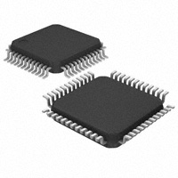
will be packaged in a single 48-pin PT (TQFP) package.
1.1 Features
•
Analog, Digital, and Monitor Amp Power Supplies: 5 V or 3.3 V
•
Differential and Single-Ended Driving of Analog Output
•
Software Power-Down Mode
•
Sample Rate Up to 11.025 kHz
•
16-Bit Signal Processing in the Codec With 2s-Complement Data Format
•
Typical 80-db Dynamic Range
•
Total Signal-to-Noise + Distortion of 80 dB for the ADCs
•
Total Signal-to-Noise + Distortion of 78 dB for the DACs
•
Programmable Gain Amplifier
•
600-Ω Driver
•
8-Ω AT41 Differential Speaker Driver With Programmable Gain Amplifier
•
Flash Write Enable Circuit Provide Power for Writing the Flash Memory Device
•
Available in 48-Pin PT (TQFP) Package Operating From –40_C to 85_C
•
Transformer Reference ( 2.5 mA Source and Sink at 2.5 V for 5 V-Supply and 1.5 V for 3.3-V Supply) to allow
Single-Ended Driving
1–1
�1.2 Functional Block Diagram
Data
Channel
Serial
Port
H
Y
B
R
I
D
Data Channel
Codec
A
M
P
Flash
Write
Enable
DRVR
Control
Logic
1.3 Analog Block Diagram
DTRX_FB
Data (Hybrid)
DTRXM
DTRXP
–
+
–
+
2.5 V
DT_REF
2.5 V/1.5 V
MonOut PGA
0/3/6/9/12 dB Gain
with Mute
Data_In PGA
0/6/12/18 dB Gain
with Mute
16-Bit
DAC
DTTX_OUTP
DTTX_INM
16-Bit
ADC
–
+
M
U
X
–
+
Data (Hybrid)
MONOUTP
2.5 V/1.5 V
–
+
+
DTTX_INP
–
8-Ω Speaker Buffer
0 dB or Mute
DTTX_OUTM
DT_BUFP
–
+
2.5 V/1.5 V
DT_BUFM
+
–
0/-6/-12/-18 dB or Mute
600-Ω Data_Out PGA
1–2
MONOUTM
�DREFM_ADC
DREFP_ADC
FILT
NC
TEST2
TEST1
MONOUTM
MV DD
MONOUTP
MV SS
TCLK
SI_SEL
1.4 Terminal Assignments
48 47 46 45 44 43 42 41 40 39 38 37
DREFP_DAC
1
DREFM_DAC
2
3
NC
NC
4
5
DAVDD
DAVSS
6
7
NC
8
NC
9
DTRX_FB
DTRXM 10
NC 11
DTRXP 12
36
35
34
33
32
31
30
29
28
27
26
25
TLC320AD545
NC
NC
DT_MCLK
DT_DIN
DT_SCLK
DT_DOUT
DT_FS
NC
RESET
DVSS
NC
NC
DT_REF
DTTX_OUTP
DTTX_INM
DTTX_INP
DTTX_OUTM
DT_BUFP
DT_BUFM
VSS
NC
DVDD
FLSH_OUT
FLSH_IN
13 14 15 16 17 18 19 20 21 22 23 24
NC–Make no external connection
1.5 Ordering Information
PACKAGE
TA
PLASTIC QUAD
FLATPACK (PT)
0°C to 70°C
TLC320AD545PT
–40°C to 85°C
TLC320AD545IPT
1.6 Terminal Functions
TERMINAL
NAME
NC
NO.
DESCRIPTION
I/O
3, 4, 7, 8,
11, 21, 25,
26, 35, 36,
45
No connection
DAVDD
DAVSS
5
I
Analog power supply (5 V/3.3 V)
6
I
Analog ground
DREFM_ADC
48
O
ADC voltage reference filter output. DREFM_ADC provides lowpass filtering for the internal bandgap
reference. The optimal ceramic capacitor value is 0.1 µF connected between DREFM_ADC and
DREFP_ADC. The nominal dc voltage at this terminal is 0 V.
DREFM_DAC
2
O
DAC voltage reference filter output. DREFM_DAC provides for lowpass filtering the internal bandgap
reference. The optimal ceramic capacitor value is 0.1 µF connected between DREFM_ADC and
DREFP_ADC. The nominal dc voltage at this terminal is 0 V.
1–3
�1.6 Terminal Functions (Continued)
TERMINAL
NAME
NO.
I/O
DESCRIPTION
DREFP_ADC
47
O
ADC voltage reference filter output. DREFP_ADC provides lowpass filtering for the internal bandgap reference.
The optimal ceramic capacitor value is 0.1 µF connected between DREFM_ADC and DREFP_ADC. The dc
voltage at this terminal is 3.375 V with a 5-V DAVDD supply and 2.25 V with a 3.3-V DAVDD supply.
DREFP_DAC
1
O
DAC voltage reference filter output. DREFP_DAC provides for lowpass filtering the internal bandgap reference.
The optimal ceramic capacitor value is 0.1 µF connected between DREFM_DAC and DREFP_DAC. The dc
voltage at this terminal is 3.375 V at 5-V DAVDD supply and 2.25 V at 3.3-V DAVDD supply.
DT_BUFM
19
O
Buffer amp analog inverting output. DT_BUFM can be programmed for 0 dB, –6 dB, –12 dB, and –18 dB gain
or muted using the control registers. This output is normally fed to the DTTX_INM terminal through an input
resistor.
DT_BUFP
18
O
Buffer amp analog noninverting output. DT_BUFP can be programmed for 0 dB, –6 dB, –12 dB and –18 dB gain
or muted using the control registers. This output is normally fed to the DTTX_INP terminal through an input
resistor. DT_BUFP must be left unconnected in single-ended hybrid.
DT_DIN
33
I
Digital data input. DT_DIN handles DAC input data as well as control register programming information during
frame sync interval and is synchronized to DT_SCLK.
DT_DOUT
31
O
Digital data output. ADC output bits transmit data during the frame sync period which is synchronized to
DT_SCLK. DT_DOUT is at high impedance when DT_FS is not activated.
DT_FS
30
O
Serial port frame sync signal. DT_FS signals the beginning of transmit for ADC data and receiving of DAC data.
This signal can be active high (FS high mode) or active low (FS low mode) depending on the voltage applied to
SI_SEL (see Section 4, Serial Communications).
DT_MCLK
34
I
Master clock input. All internal clocks are derived from this clock.
DT_REF
13
O
Reference voltage for the transformer at 2.5 V for a 5-V DAVDD supply and 1.5 V for a 3.3-V DAVDD supply. The
maximum source or sink current at this terminal is 2.5 mA. DT_REF must be left unconnected in differential hybrid.
9
O
Receive path amplifier feedback node. DTRX_FB terminal is connected to the noninverting output of the receive
path amplifier and allows a parallel resistor/capacitor to be placed in the amplifier feedback path for setting gain
and filter poles.
DTRXM
10
I
Receive path amplifier analog inverting input
DTRXP
12
I
Receive path amplifier analog noninverting input
DT_SCLK
32
O
Shift clock signal. DT_SCLK clocks serial data into DT_DIN and out of DT_DOUT during the frame-sync interval.
DT_SCLK rate is DT_MCLK/2.
DTTX_INM
15
I
Transmit amplifier analog inverting input. This node is normally fed by the DT_BUFM output through an input
resistor.
DTTX_INP
16
I
Transmit amplifier analog noninverting input. This node is normally fed by the DT_BUFP output through an input
resistor. DTTX_INP must be shorted to DTTX_OUTM in single-ended hybrid.
DTTX_OUTM
17
O
Transmit amplifier analog inverting output. DTTX_OUTM must be shorted to DTTX_INP in single-ended hybrid.
DTTX_OUTP
14
O
Transmit amplifier analog noninverting output
DVDD
22
I
Digital and RESET circuit power supply (5 V/3.3 V)
DVSS
27
I
Digital and RESET circuit ground
FILT
46
O
Bandgap filter node. FILT provides decoupling of the bandgap reference voltage. This reference is 3.375 V with
a 5-V supply and 2.25 V with a 3.3-V supply. The optimal capacitor value is 0.1 µF (ceramic). This node should
not be used as a voltage source.
FLSH_IN
24
I
External ASIC logic input. When brought low, FLSH_IN enables the FLSH_OUT output.
FLSH_OUT
23
O
Power output to write/erase flash EEPROM device (such as Intel 28F400B or AMD Am29F400). Supplies 45
mA maximum from 5 V when FLSH_IN is brought low.
MONOUTM
42
O
Analog output from 8-Ω monitor speaker amplifier which can be set for 0-dB gain or muted through the control
registers.
MONOUTP
40
O
Analog output from 8-Ω monitor speaker amplifier which can be set for 0-dB gain or muted through the control
registers.
DTRX_FB
Intel is a trademark of Intel Systems, Inc.
AMD is a trademark of Advanced Micro Devices, Inc.
1–4
�1.6 Terminal Functions (Continued)
TERMINAL
NAME
NO.
DESCRIPTION
I/O
MVDD
MVSS
41
I
Monitor amplifier supply (5 V/3.3 V)
39
I
Monitor amplifier ground
RESET
28
I
Codec device reset. RESET initializes all device internal registers to default values. This signal is active low.
SI_SEL
37
I
Serial interface mode select. When SI_SEL is tied to DVDD, the serial port is in FS high mode. When SI_SEL is
tied to DVSS, the serial port is in FS low mode. (see Section 4, Serial Communications).
TCLK
38
O
Test output port. TCLK is for factory test only and should be either connected to ground or left unconnected.
TEST1
43
I/O
Test input port. TEST1 is for factory test only and should be either connected to ground or left unconnected.
TEST2
44
I/O
Test input port. TEST2 is for factory test only and should be either connected to ground or left unconnected.
VSS
20
I
Internal substrate connection. VSS should be tied to DAVSS .
1–5
�1–6
�2 Functional Description
2.1 Device Requirements and System Overview
The TLC320AD545 device consists of single codec channel, a hybrid circuit with external resistors and capacitors
for setting gain and filter poles, serial port, and miscellaneous other logic functions.
2.2 Codec Functions
The codec portion of the device performs the functions for:
•
One channel of analog-to-digital conversion
•
Digital-to-analog conversion
•
Lowpass filtering
•
Control of analog input and output gains
•
Internal oversampling coupled with internal decimation and interpolation
•
A 16-bit serial port interface to the host processor.
The maximum sample rate is 11.025 kHz.
2.3 Hybrid Functions
The hybrid circuitry has integrated amplifiers whose gains and filter pole frequencies are set by external resistors and
capacitors. This allows maximum flexibility to make adjustments for board variations and international standards
while providing integration of the function. The filter amplifier stages are followed by a programmable gain amplifier,
which feeds an 8 Ω differential speaker driver for the AT41 call progress monitor speaker. The monitor speaker driver
can be programmed for 0 dB gain or muted through control register 2. The source for the monitor speaker input can
be chosen to be either the amplified DAC output (Data_Out PGA) or the ADC input signal through control register
1 (see Appendix A).
A 2.5 V/1.5 V reference voltage (DT_REF) is provided as a reference for the transformer. It is necessary to reference
to 2.5 V/1.5 V (rather than ground), since the amplifiers are powered off by single-rail supplies. DT_REF is 2.5 V when
DAVDD is 5 V and 1.5 V when DAVDD is 3.3 V.
2.4 Miscellaneous Logic and Other Circuitry
The logic functions include the circuitry required to implement serial port and control register programming through
secondary communication on those serial ports. Two control registers can be programmed during secondary
communications from the serial port. These control registers set amplifier gains, select loopback functions, and read
ADC overflow flags. In addition, a flash write enable (FWE) circuit takes an external logic input and provides current
to power the write enable circuit of an external memory device. The flash write enable circuit is powered from the
digital power supply.
2–1
�2–2
�3 Codec Functional Description
3.1 Operating Frequencies
The TLC320AD545 is capable of supporting any sample rate up to the maximum sample rate of 11.025 kHz. The
sample rate is set by the frequency of the codec master clock.
The sampling (conversion) frequency is derived from the codec master clock by the internal clock divider circuit by
equation (1):
DT_FS= Sampling (conversion) frequency = DT_MCLK/512
(1)
The shift clock (SCLK) is derived from the codec master clock divider circuit by equation (2):
DT_SCLK (frequency)= DT_MCLK/2
(2)
Where MCLK is codec clock fed to the codec externally by the clock rate divider circuit which divides the system
master clock to get the necessary clock frequency to feed the codec.
The conversion period is the inverse of sampling frequency.
3.2 ADC Signal Channel
The input signals are amplified and filtered by on-chip buffers before being applied to ADC input. The ADC converts
the signal into discrete output digital words in 2s-complement format, corresponding to the analog signal value at the
sampling time. These 16-bit digital words, representing sampled values of the analog input signal, are sent to the host
through the serial port interface. If the ADC reaches its maximum value, a control register flag is set. This overflow
bit resides at D0 in control register 2. This bit can only be read from the serial port, and the overflow flag is only cleared
if it is read through the serial port. The ADC and DAC conversions are synchronous and phase-locked.
3.3 DAC Signal Channel
The DAC receives 16-bit data words (2s complement) from the host through the serial port interface. The data is
converted to an analog voltage by the sigma-delta DAC comprised of a digital interpolation filter and a digital
modulator. The DAC output is then passed to an internal low-pass filter to complete the signal reconstruction resulting
in an analog signal. This analog signal is then buffered and amplified by differential output driver capable of driving
the required load. The gain of the DAC output amplifier is programmed by the codec control register as shown in
Appendix A.
3.4 Sigma-Delta ADC
The ADC is an oversampling sigma-delta modulator. The ADC provides high resolution and low noise performance
using oversampling techniques and the noise shaping advantages of sigma-delta modulators.
3.5 Decimation Filter
The decimation filter reduces the digital data rate to the sampling rate. This is accomplished by decimating with a ratio
equal to the oversampling ratio. The output of this filter is a sixteen-bit 2s-complement data word clocking at the
selected sample rate.
3.6 Sigma-Delta DAC
The DAC is an oversampling sigma-delta modulator. The DAC perform high-resolution, low-noise digital-to-analog
conversion using oversampling sigma-delta techniques.
3–1
�3.7 Interpolation Filter
The interpolation filter resamples the digital data at a rate of N times the incoming sample rate where N is the
oversampling ratio. The high-speed data output from this filter is then applied to the sigma-delta DAC.
3.8 Analog and Digital Loopbacks
The test capabilities include an analog loopback and digital loopback. The loopbacks provide a means of testing the
ADC/DAC channels and can be used for in-circuit system-level tests.
Analog loopback loops the DAC output back into the ADC input. Digital loopback loops the ADC output back into the
DAC input. Analog loopback is enabled by setting bit D4 in the control register 1. Digital loopback is enabled by setting
bit D5 high in control register 1. The analog loopback function tests only the codec portion of the device and does
not include the hybrid amplifier.
3.9 Software Power Down
The software power down resets all internal counters but leaves the contents of the programmable control registers
unchanged. The software power down feature is invoked by setting bit D6 high in control register 1. There is no
hardware power down function in the TLC320AD545.
3.10 Test Module
The test module serves the purpose of facilitating design verification test and simplifying factory production testing.
There are three input/output terminals (TEST1, TEST2 and TCLK) dedicated to implementing the test functions. The
function of these terminals is for factory self-test only and no connection (NC) should be made to either of these
terminals.
3.11 Power Supply Options
ANALOG SUPPLY
(DAVDD)
3–2
DIGITAL SUPPLY
(DVDD)
MONITOR SUPPLY
(MVDD)
Option 1
5V
5V
5V
Option 2
3.3 V
3.3 V
3.3 V
Option 3
5V
3.3 V
5V
�4 Serial Communications
DT_DOUT, DT_DIN, DT_SCLK, and DT_FS, are the serial communication signals for the serial port. The digital
output data from the ADC is taken from DT_DOUT. The digital input data for the DAC is applied to DT_DIN. The
synchronization clock for the serial communication data and the frame-sync is taken from DT_SCLK. The frame-sync
pulse, which signals the beginning of the ADC and DAC data transfer interval, is taken from DT_FS.
For signal data transmitted from the ADC or to the DAC, a primary serial communication is used. A secondary
communication is used to read or write words to the control registers, which control both the options and the circuit
configurations of the device.
The purpose of the primary and secondary communications is to allow conversion data and control data to be
transferred across the same serial port. A primary transfer is always dedicated to conversion data. A secondary
transfer is used to set up or read the control register values described in Appendix A, Programmable Register Set.
A primary transfer occurs for every conversion period. A secondary transfer occurs only when requested. Secondary
serial communication is requested by software (D0 of the primary data input to DT_DIN). Control registers 1 and 2
can only be read/write from/to the serial port.
4.1 Primary Serial Communication
Primary serial communication is used to both transmit and receive conversion signal data. The DAC word length is
15 bits and the last bit of the primary 16-bit serial communication word is a control bit used to request secondary serial
communication. For all serial communications, the most significant bit is transferred first. For the 16-bit ADC word,
D15 is the most significant bit and D0 is the least significant bit. For the 15-bit DAC data word in a primary
communication, D15 is the most significant bit, D1 is the least significant bit, and D0 is used for the secondary
communication request control. All digital data values are in 2s-complement data format. Refer to Figure 4–1.
DT_DIN
D15–D1
D0
D/A Data
Secondary
Communication Request
A/D Data
DT_DOUT
D15–D0
Figure 4–1. Primary Communication DIN and DOUT Data Format
4–1
�4.1.1
FS High Mode Primary Communication Timing
There are two possible modes for serial data transfer. One mode is the FS high mode, which is selected by tying the
SI_SEL terminal to DVDD. Figure 4–2 shows the timing relationship for DT_SCLK, DT_FS, DT_DOUT and DT_DIN
in a primary communication when in FS high mode. The timing sequence for this operation is as follows:
1. DT_FS is brought high and remains high for one DT_SCLK period, then goes back low.
2. A 16-bit word is transmitted from the ADC (DT_DOUT) and a 16-bit word is received for DAC conversion
(DT_DIN).
DT_SCLK
DT_FS
DT_DIN
D15 D14 D13 D12 D11 D10
D9
D8
D7
D6
D5
D4
D3
D2
D1
D0
DT_DOUT
D15 D14 D13 D12 D11 D10
D9
D8
D7
D6
D5
D4
D3
D2
D1
D0
Figure 4–2. FS High Mode Primary Serial Communication Timing
4.1.2
FS Low Mode Primary Communication Timing
The second possible serial interface mode is the FS low mode which is selected by tying the SI_SEL terminal to DVSS.
This mode differs from the FS high mode in that the frame sync signal (FS) is active low, data transfer starts on the
falling edge of DT_FS, and DT_FS remains low throughout the data transfer. Figure 4–3 shows the timing relationship
for DT_SCLK, DT_FS, DT_DOUT, and DT_DIN in a primary communication when in FS low mode. The timing
sequence for this operation is as follows:
1. DT_FS is brought low by the TLC320AD545.
2. A 16-bit word is transmitted from the ADC (DT_DOUT) and a 16-bit word is received for DAC conversion
(DT_DIN).
3. DT_FS is brought high signaling the end of the data transfer.
4–2
�DT_SCLK
DT_FS
DT_DIN
D15 D14 D13 D12 D11 D10
D9
D8
D7
D6
D5
D4
D3
D2
D1
D0
DT_DOUT
D15 D14 D13 D12 D11 D10
D9
D8
D7
D6
D5
D4
D3
D2
D1
D0
Figure 4–3. FS Low Mode Primary Serial Communication Timing
4.2 Secondary Serial Communication
Secondary serial communication is used to read or write 16-bit words that program both the options and the circuit
configurations of the device. Register programming always occurs during secondary communication. Control
registers 1 and 2 can only be written to or read from the serial port. Two primary and secondary communication cycles
are necessary to program the control registers. If the default value for a particular register is desired, then the register
addressing can be omitted during secondary communications. The NOOP (no operation) command addresses a
pseudo-register, register 0, and no register programming takes place during this secondary communication.
During a secondary communication, a register may be written to or read from. When writing a value to a register, the
DT_DIN line contains the value to be written. The data returned on DT_DOUT is 00h.
The method for requesting a secondary communication is by asserting the least significant bit (D0) of DT_DIN high
as shown in Table 4–1.
Table 4–1. Least-Significant-Bit Control Function
CONTROL BIT D0
CONTROL BIT FUNCTION
0
No secondary communication request
1
Secondary communication request
Figure 4–4 shows the data format XX_DIN and XX_DOUT during secondary communication.
Don’t Care
D15
DT_DIN
(Read)
––
––
1
R/W
D12 D11 D10
D9
D8
Register Address
D7–D0
Register Data
D15
DT_DIN
(Write)
DT_DOUT
(Read)
––
––
0
D12 D11 D10
D9
D8
D7–D0
AII 0
Register Data
D15–D8
D7–D0
AII 0
DT_DOUT
(Write)
D15–D0
Figure 4–4. Secondary Communication DIN and DOUT Data Format
4–3
�4.3 FS High Mode Secondary Communication Timing
On the rising edge of DT_SCLK, coinciding with the falling edge of FS, D15–D0 is input serially to DT_DIN and
D15–D0 is output serially on DT_DOUT. If a secondary communication request is made, FS goes high again, 128
SCLKs after the beginning of the primary frame, to signal the beginning of the secondary frame one SCLK period later.
See Figure 4–5.
128 DT_SCLKs
P
S
P
P
DT_FS
DT_DIN
Data (D0=1)
Register R/W
Secondary Communication
Request
Data (D0=0)
No Secondary
Communication Request
ÎÎÎ
ÎÎÎ
Figure 4–5. FS Output During Software Secondary Serial Communication Request
(FS High Mode)
4.4 FS Low Mode Secondary Communication Timing
On the falling edge of FS for that channel, D15–D0 is input serially to DT_DIN and D15–D0 is output serially on
DT_DOUT. FS remains low during the data transfer and then returns high. If a secondary communication request is
made, FS goes low 128 SCLKs after the beginning of the primary frame to signal the beginning of the secondary
frame. See Figure 4–6.
128 DT_SCLKs
DT_FS
DT_DIN
P
S
P
Data (D0=1)
Register R/W
Data (D0=0)
Secondary Communication
Request
No Secondary
Communication Request
Figure 4–6. FS Output During Software Secondary Serial Communication Request
(FS Low Mode)
4–4
�5 Specifications
5.1 Absolute Maximum Ratings Over Operating Free-Air Temperature Range
(Unless Otherwise Noted)
Supply voltage range, DVDD, AVDD, (see Note 1) . . . . . . . . . . . . . . . . . . . . . . . . . . . . . . . . . . . . . . –0.3 V to 7 V
Output voltage range, all digital output signals . . . . . . . . . . . . . . . . . . . . . . . . . . . . . . . . . . –0.3 V to DVDD+0.3 V
Input voltage range, all digital input signals . . . . . . . . . . . . . . . . . . . . . . . . . . . . . . . . . . . . –0.3 V to DVDD+0.3 V
Case temperature for 10 seconds: PM package . . . . . . . . . . . . . . . . . . . . . . . . . . . . . . . . . . . . . . . . . . . . . . 260_C
Operating free-air temperature range, TA . . . . . . . . . . . . . . . . . . . . . . . . . . . . . . . . . . . . . . . . . . . . . –40_C to 85_C
Storage temperature range, Tstg . . . . . . . . . . . . . . . . . . . . . . . . . . . . . . . . . . . . . . . . . . . . . . . . . . . . –65_C to 150_C
† Stresses beyond those listed under “absolute maximum ratings” may cause permanent damage to the device. These are stress ratings only and
functional operation of the device at these or any other conditions beyond those indicated under “recommended operating conditions” is not
implied. Exposure to absolute-maximum-rated conditions for extended periods may affect device reliability.
NOTE 1: All voltage values are with respect to Vss.
5.2 Recommended Operating Conditions
Supply voltage, DAVDD, MVDD, DVDD (5-V supply)
Supply voltage, DAVDD, MVDD, DVDD (3.3-V supply) (see Note 2)
Analog signal peak-to-peak input voltage‡, DTRXM, DTRXP, VI(analog) (5-V supply)
MIN
NOM
MAX
4.5
5
5.5
V
3
3.3
3.6
V
3
V
2
V
Analog signal peak-to-peak input voltage‡, DTRXM, DTRXP, VI(analog) (3.3-V supply)
Differential output load resistance, RL (DT_BUFP, DT_BUFM)
Differential output load resistance, RL (MONOUTP, MONOUTM)
Ω
600
Ω
8
Input impedance for hybrid amps (DTRXP, DTRXM, DTTX_INP, DTTX_INM)
50
Master clock
Operating free-air temperature, TA
kΩ
5.645
Load capacitance, CL
ADC or DAC conversion rate
8
0
UNIT
MHz
20
pF
11.025
kHz
70
°C
‡ Preamplifier gain set to 0 dB
NOTE 2: Voltages at analog inputs and outputs and xVDD are respect to the xVSS terminal.
5–1
�5.3 Electrical Characteristics Over Recommended Operating Free-Air
Temperature Range DVDD = 5 V/3.3 V, AVDD = 5 V/3.3 V, MVDD = 5 V/3.3 V
5.3.1
Digital Inputs and Outputs, fs = 8 kHz, Outputs Not Loaded
PARAMETER
TEST CONDITIONS
MIN
TYP
MAX
UNIT
2.4
DVDD
+ 0.5
V
DVSS
– 0.5
0.4
V
10
µA
10
µA
VOH
High-level output voltage, any digital output
IO = –360 µA
VOL
Low-level output voltage, any digital output
IO = 2 mA
IIH
IIL
High-level input current, any digital input
VIH = 5 V
VIL = 0.6 V
Cj
Input capacitance, any digital input
10
pF
CO
Output capacitance, any digital output
10
pF
II(lkg)
IOZ
Input leakage current, any digital input
10
µA
Output leakage current, any digital output
10
µA
5.3.2
Low-level input current, any digital input
ADC Channel, fs = 8 kHz (see Note 3)
PARAMETER
Filter gain relative to gain at 1020 Hz
TEST CONDITIONS
MIN
0 to 300 Hz
–0.5
TYP
0.2
300 Hz to 3 kHz
–0.25
0.25
3.3 kHz
–0.35
0.3
3.6 kHz
MAX
–3
4 kHz
–35
≥4.4 kHz
–74
UNIT
dB
NOTE 3: The filter gain outside of the passband is measured with respect to the gain at 1020 Hz. The analog input test signal is a sine wave with
0 dB=3 VPP at 5-V supply and 0 db = 2 VPP at 3.3-V supply differential as the reference level for ADC analog input signal. The –3 dB
passband is 0 to 3600 Hz for an 8-kHz sample rate. This passband scales linearly with the sample rate.
5.3.3
ADC Dynamic Performance, fs = 8 kHz
5.3.3.1 ADC Signal-to-Noise (see Note 4)
PARAMETER
TEST CONDITIONS
VI = –1 dB
VI = –9 dB
Signal-to-noise ratio (SNR)
MIN
TYP
76
81
68
73
MAX
UNIT
dB
VI = –40 dB
37
42
NOTE 4: The test condition is a 1020-Hz input signal with an 8-kHz conversion rate. Input and output common mode is 2.5 V for 5 V supply and
1.5 V for 3.3 V supply. The output configuration is in a 5 V differential-ended mode.
5.3.3.2 ADC Signal-to-Distortion (see Note 4)
PARAMETER
Signal-to-total harmonic distortion (THD)
TEST CONDITIONS
VI = –3 dB
VI = –9 dB
MIN
TYP
74
79
82
87
MAX
UNIT
dB
VI = –40 dB
58
63
NOTE 4: The test condition is a 1020-Hz input signal with an 8-kHz conversion rate. Input and output common mode is 2.5 V for 5 V supply and
1.5 V for 3.3 V supply. The output configuration is in a 5 V differential-ended mode.
5–2
�5.3.3.3 ADC Signal-to-Distortion + Noise (see Note 4)
PARAMETER
Signal-to-total harmonic distortion + noise (THD + N)
MIN
TYP
VI = –3 dB
VI = –9 dB
TEST CONDITIONS
71
76
68
73
VI = –40 dB
37
42
MAX
UNIT
dB
NOTE 4: The test condition is a 1020-Hz input signal with an 8-kHz conversion rate. Input and output common mode is 2.5 V for 5-V supply and
1.5 V for 3.3-V supply. The output configuration is in a 5 V differential-ended mode.
5.3.4
ADC Characteristics
PARAMETER
VI(PP)
VI(PP)
TEST CONDITIONS
MIN
MAX
UNIT
Peak-input voltage (5.0 V supply)
Preamp gain = 0 dB
3
V
Peak-input voltage (3.3 V supply)
Preamp gain = 0 dB
2
V
Dynamic range
VI =–1 dB at 1020 Hz
80
dB
87
dB
VI = –1 dB at 1020 Hz
±0.5
dB
VI = –1 dB at 1020 Hz
80
Interchannel isolation
EG
EO(ADC)
Gain error
CMRR
Common-mode rejection ratio
ADC channel offset error including hybrid amplifiers
3
Idle channel noise (on-chip reference)
50
Channel delay
5.3.5
TYP
12
mV
dB
100
17/fs
µVrms
s
DAC Channel, fs = 8 kHz (see Note 5)
PARAMETER
TEST CONDITIONS
0 to 300 Hz
Filter gain relative to gain at 1020 Hz
MIN
TYP
MAX
–0.5
0.2
300 Hz to 3 kHz
–0.25
0.25
3.3 kHz
–0.35
0.3
3.6 kHz
UNIT
dB
–3
4 kHz
–35
NOTE 5: The filter gain outside of the passband is measured with respect to the gain at 1020 Hz. The input signal is the digital equivalent of a
sine wave (digital full scale = 0 dB). The –3 dB pass band is 0 to 3600 Hz for an 8-kHz sample rate. This pass band scales linearly
with the sample rate.
5.3.6
DAC Dynamic Performance
5.3.6.1 DAC Signal-to-Noise (see Note 6)
PARAMETER
TEST CONDITIONS
VI = 0 dB
VI = –9 dB
Signal-to-noise ratio (SNR)
MIN
TYP
72
77
63
68
MAX
UNIT
dB
VI = –40 dB
32
37
NOTE 6: The test condition is a 1020-Hz input signal with an 8-kHz conversion rate. The output configuration is in a 5 V differential-ended mode.
5.3.6.2 DAC Signal-to-Distortion (see Note 6)
PARAMETER
Signal-to-total harmonic distortion (THD)
TEST CONDITIONS
VI = –3 dB
VI = –9 dB
MIN
TYP
77
82
72
77
MAX
UNIT
dB
VI = –40 dB
61
66
NOTE 6: The test condition is a 1020-Hz input signal with an 8-kHz conversion rate. The output configuration is in a 5 V differential-ended mode.
5–3
�5.3.6.3 DAC Signal-to-Distortion + Noise (see Note 6)
PARAMETER
Signal-to-total harmonic distortion + noise (THD + N)
MIN
TYP
VI = –3 dB
TEST CONDITIONS
73
78
VI = –9 dB
67
72
VI = –40 dB
32
37
MAX
UNIT
dB
NOTE 6: The test condition is a 1020-Hz input signal with an 8-kHz conversion rate. The output configuration is in a 5 V differential-ended mode.
5.3.7
DAC Characteristics
PARAMETER
TEST CONDITIONS
Dynamic range
MIN
VI = 0 dB at 1020 Hz
Interchannel isolation
EG
Gain error
MAX
dB
100
dB
dB
75
Channel delay
UNIT
82
±0.5
VI = 0 dB at 1020 Hz
0 kHz to 4 kHz (see Note 7)
Idle channel narrow-band noise
TYP
125
18/fs
µV rms
s
VO
Analog output voltage, MONOUTP-MONOUTM (5.0 V)
Differential with respect to common
mode and full-scale digital input (see
Note 8)
VO
Analog output voltage, MONOUTP-MONOUTM (3.3 V)
Differential with respect to common
mode and full-scale digital input (see
Note 8)
VO
Analog output voltage (5 V)
Differential with respect to common
mode and full-scale digital input
–3
3
V
VO
Analog output voltage, (3.3 V)
Differential with respect to common
mode and full-scale digital input
–2
2
V
–1.78
1.78
V
–1.2
1.2
V
NOTES: 7. The conversion rate is 8 kHz.
8. This amplifier should only be used in differential mode. Common mode : 2.5 V in 5-V supply, 1.5 V in 3.3-V supply.
5.3.8
Logic DC Electrical Characteristics
PARAMETER
MIN
TYP
VIL
VIH
Low-level input voltage
–0.3
High-level input voltage
2
II(lkg)
IO(lkg)
VOH
VOL
High-level output voltage at rated load current
2.4
Low-level output voltage at rated load current
DVSS–0.5
5.3.9
MAX
UNIT
0.8
V
DVDD+0.3
V
Input leakage current
10
µA
Output leakage current
10
µA
DVDD+0.5
V
0.4
V
Power-Supply Rejection (see Note 9)
PARAMETER
VDD1
VDD2
Supply-voltage rejection ratio, ADC channel, DAVDD
VDD3
VDD4
Supply-voltage rejection ratio, ADC channel, DVDD
Supply-voltage rejection ratio, DAC channel, DAVDD
Supply-voltage rejection ratio, DAC channel, DVDD
TEST CONDITIONS
MIN
TYP
fI = 0 to fs/2
fI = 0 to fs/2
73
fI = 0 to fs/2
fI = 0 to 30 kHz
86
76
MAX
UNIT
dB
95
NOTE 9: Power supply rejection measurements are made with both the ADC and the DAC channels idle and a 200 mV peak-to-peak signal
applied to the appropriate supply.
5–4
�5.3.10 Power-Supply
PARAMETER
TEST CONDITIONS
MIN
TYP
IDD (analog)
Codec power supply
y current,, analog
g ((including
g
hybrid and drivers)
DAVDD = 5 V
DAVDD = 3.3 V
Operating
25
Operating
20
IDD (digital )
Codec power supply current
current, digital
DAVDD = 5 V
DAVDD = 3.3 V
Operating
5
Operating
4
IDD (monitor)
IDD (monitor)
Power supply current, 8 Ω monitor speaker driver (5 V)
Operating
135
Power supply current, 8 Ω monitor speaker driver (3.3 V)
Operating
MAX
UNIT
mA
mA
315
mA
240
mA
MAX
UNIT
5.3.11 Flash Write Enable Circuit
PARAMETER
TEST CONDITIONS
MIN
TYP
VOH(FLSH_OUT)
Output high-level voltage (5 V supply), FLSH_OUT
FLSH_IN low
4.5
5
5.5
V
VOH(FLSH_OUT)
Output high-level voltage (3.3 V supply), FLSH_OUT
FLSH_IN low
2.8
3.3
3.8
V
VOL(FLSH_OUT)
Output low-level voltage, FLSH_OUT
FLSH_IN high
1.5
V
IO(FLSH_OUT)
Output current (5 V supply), FLSH_OUT
FLSH_IN low
40
45
mA
IO(FLSH_OUT)
Output current (3.3 V supply), FLSH_OUT
FLSH_IN low
25
0
mA
5.4 Timing Characteristics (see Parameter Measurement Information)
5.4.1
Timing Requirements
PARAMETER
MIN
TYP
MAX
0
UNIT
td1
tsu1
Delay time, DT_SCLK↑ to DT_FS↓
th1
td3
Hold time, DT_DIN, after DT_SCLK high
20
ns
Delay time, DT_MCLK↓ to DT_SCLK↑
50
ns
twH
twL
Pulse duration, DT_MCLK high
32
ns
Pulse duration, DT_MCLK low
20
ns
Setup time, DT_DIN, before DT_SCLK low
5.4.2
Switching Characteristics
td2
ten1
Delay time, DT_SCLK↑ to DT_DOUT
tdis1
TPW
Disable time, FS↑ to DT_DOUT Hi-Z
PARAMETER
Enable time, FS↓ to DT_DOUT
Reset pulse width
25
TEST CONDITIONS
MIN
ns
ns
TYP
MAX
UNIT
20
CL = 20 pF
25
ns
20
10MCLK
ns
5–5
�5.5 Parameter Measurement Information
twH
DT_MCLK
td3
twL
DT_SCLK
td1
DT_FS
tdis1
td2
D15
DT_DOUT
ten1
D14
tsu1
DT_DIN
D15
D14
th1
Figure 5–1. Serial Communication Timing
0
–20
Attenuation – dB
–40
–60
–80
–100
– 120
0.8
1.6
2.4
3.2
4
4.8
fI – Input Frequency – kHz
5.6
6.4
Figure 5–2. ADC Decimation Filter Response
5–6
7.2
�0.8
0.6
Attenuation – dB
0.4
0.2
0
–0.2
–0.4
–0.6
–0.8
0.4
0.8
1.2
1.6
2
2.4
fI – Input Frequency – kHz
2.8
3.2
Figure 5–3. ADC Decimation Filter Passband Ripple
0
–20
Attenuation – dB
–40
–60
–80
–100
– 120
0.8
1.6
2.4
3.2
4
4.8
fI – Input Frequency – kHz
5.6
6.4
7.2
Figure 5–4. DAC Interpolation Filter Response
5–7
�0.8
0.6
Attenuation – dB
0.4
0.2
0
–0.2
–0.4
–0.6
–0.8
0.4
0.8
1.2
1.6
2
2.4
fI – Input Frequency – kHz
2.8
Figure 5–5. DAC Interpolation Filter Passband Ripple
5–8
3.2
�6 Application Information
Data
Channel
Serial
Port
Data Channel
Codec
H
Y
B
R
I
D
Matching
Network
POTS
A
M
P
Flash
Write
Enable
Control
Logic
DRVR
AT41
SPKR
Figure 6–1. Functional Block of a Typical Application
6–1
�DTRX_FB
Data (Hybrid)
{
{
{
DTRXM
{
–
{
T1
{
–
+
{
{
{
DTRXP
2.5 V/1.5 V
{
16-Bit
DAC
DTTX_OUTP
{
MonOut PGA
0/3/6/9/12 dB Gain
with Mute
Data_In PGA
0/6/12/18 dB Gain
with Mute
DT_REF
2.5 V/1.5 V
Primary
Line
16-Bit
ADC
+
–
M
U
X
+
{
MONOUTP
AT41
{
DTTX_INM
–
+
Data (Hybrid)
+
8-Ω Speaker Buffer
0 dB or Mute
2.5 V/1.5 V
DTTX_INP
–
+
–
{
{
{
DTTX_OUTM
DT_BUFP
–
+
2.5 V/1.5 V
DT_BUFM
+
–
0/-6/-12/-18 dB or Mute
600-Ω Data_Out PGA
† Required to meet communication standards
Figure 6–2. Differential Configuration Typical Application
6–2
MONOUTM
�DTRX_FB
Data (Hybrid)
{
{
DTRXM
{
–
+
{
T1
{
{
{
–
+
16-Bit
ADC
Data_In PGA
0/6/12/18 dB Gain
with Mute
2.5 V/1.5 V
DT_REF
2.5 V/1.5 V
Primary
Line
16-Bit
DAC
{
Mon_Out PGA
0/3/6/9/12 dB Gain
with Mute
DTRXP
–
+
M
U
X
DTTX_OUTP
{
MONOUTP
AT41
{
DTTX_INM
–
+
Data (Hybrid)
8-Ω Speaker Buffer
0 dB or Mute
2.5 V/1.5 V
DTTX_INP
–
+
+
–
MONOUTM
DTTX_OUTM
–
DT_BUFP(NC)
+
2.5 V/1.5 V
DT_BUFM
+
–
0/-6/-12/-18 dB or Mute
600-Ω Data_Out PGA
† Required to meet communication standards
Figure 6–3. Single-Ended Configuration Typical Application
6–3
�6–4
�Appendix A
Programmable Register Set
Bits D12–D8 in a secondary serial communication comprise the address of the register that is written with data carried
in bits D7–D0. D13 determines a read or write cycle to the addressed register. When low (0), a write cycle is selected.
The following table shows the register map.
Table A–1. Register Map
REGISTER NO.
D15
D14
D13
D12
D11
D10
D9
D8
REGISTER NAME
1
0
0
R/W
0
0
0
0
1
Control 1
2
0
0
R/W
0
0
0
1
0
Control 2
Table A–2. Control Register 1
D7
D6
D5
D4
D3
D2
D1
D0
DESCRIPTION
1
Software reset asserted
0
Software reset not asserted
1
S/W power down enabled
0
S/W power down disabled
1
Digital loopback asserted
0
Digital loopback not asserted
1
Analog loopback asserted
0
Analog loopback not asserted
1
Select data_in PGA for monitor amp input
0
Select DAC output for monitor amp input
1
0
1
Monitor amp PGA gain = 12 dB
1
0
0
Monitor amp PGA gain = 9 dB
0
1
1
Monitor amp PGA gain = 6 dB
0
1
0
Monitor amp PGA gain = 3 dB
0
0
1
Monitor amp PGA gain = 0 dB
0
0
0
Monitor amp PGA gain = mute
Default value: 00000000
A–1
�Table A–3. Control Register 2
D7
D6
D5
D4
D3
D2
D1
D0
1
0
0
Data in (DTRX) PGA gain = mute
0
1
1
Data in (DTRX) PGA gain = 18 dB
0
1
0
Data in (DTRX) PGA gain = 12 dB
0
0
1
Data in (DTRX) PGA gain = 6 dB
0
0
0
Data in (DTRX) PGA gain = 0 dB
1
0
0
DAC data out PGA gain = mute
0
1
1
DAC data out PGA gain = –18 dB
0
1
0
DAC data out PGA gain = –12 dB
0
0
1
DAC data out PGA gain = –6 dB
0
0
0
DAC data out PGA gain = 0 dB
1
8 Ω monitor speaker driver gain = 0 dB
0
8 Ω monitor speaker driver gain = mute
X
ADC overflow indicator: ← 1 = overflow
Default value: 00000000
A–2
DESCRIPTION
�PACKAGE OPTION ADDENDUM
www.ti.com
10-Dec-2020
PACKAGING INFORMATION
Orderable Device
Status
(1)
Package Type Package Pins Package
Drawing
Qty
Eco Plan
(2)
Lead finish/
Ball material
MSL Peak Temp
Op Temp (°C)
Device Marking
(3)
(4/5)
(6)
TLC320AD545IPT
ACTIVE
LQFP
PT
48
250
RoHS & Green
NIPDAU
Level-1-260C-UNLIM
-40 to 85
320AD545I
TLC320AD545PTR
ACTIVE
LQFP
PT
48
1000
RoHS & Green
NIPDAU
Level-1-260C-UNLIM
0 to 70
320AD545
(1)
The marketing status values are defined as follows:
ACTIVE: Product device recommended for new designs.
LIFEBUY: TI has announced that the device will be discontinued, and a lifetime-buy period is in effect.
NRND: Not recommended for new designs. Device is in production to support existing customers, but TI does not recommend using this part in a new design.
PREVIEW: Device has been announced but is not in production. Samples may or may not be available.
OBSOLETE: TI has discontinued the production of the device.
(2)
RoHS: TI defines "RoHS" to mean semiconductor products that are compliant with the current EU RoHS requirements for all 10 RoHS substances, including the requirement that RoHS substance
do not exceed 0.1% by weight in homogeneous materials. Where designed to be soldered at high temperatures, "RoHS" products are suitable for use in specified lead-free processes. TI may
reference these types of products as "Pb-Free".
RoHS Exempt: TI defines "RoHS Exempt" to mean products that contain lead but are compliant with EU RoHS pursuant to a specific EU RoHS exemption.
Green: TI defines "Green" to mean the content of Chlorine (Cl) and Bromine (Br) based flame retardants meet JS709B low halogen requirements of


 工商网监
湘ICP备2023018690号
工商网监
湘ICP备2023018690号
