������� ������� �������
�
���
���������� ���� ����������
SLCS119B − DECEMBER 1986 − REVISED DECEMBER 2006
D Very Low Power . . . 200 µW Typ at 5 V
D Fast Response Time . . . 2.5 µs Typ With
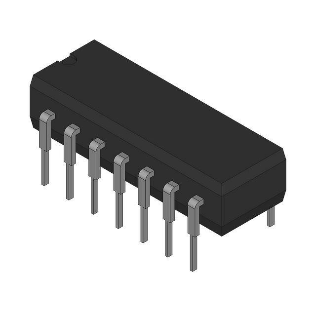
D, J, N, OR PW PACKAGE
(TOP VIEW)
5-mV Overdrive
1OUT
2OUT
VDD
2IN −
2IN +
1IN −
1IN +
D Single Supply Operation:
D
14
2
13
3
12
4
11
5
10
6
9
7
8
3OUT
4OUT
GND
4IN +
4IN −
3IN +
3IN −
FK PACKAGE
(TOP VIEW)
2OUT
1OUT
NC
3OUT
3OUT
D
D
TLC139M . . . 4 V to 16 V
TLC339M . . . 4 V to 16 V
TLC339C . . . 3 V to 16 V
TLC339I . . . 3 V to 16 V
High Input Impedance . . . 1012 Ω Typ
Input Offset Voltage Change at Worst Case
Input at Condition Typically 0.23 µV/Month
Including the First 30 Days
On-Chip ESD Protection
1
description
VDD
NC
2IN −
NC
2IN +
The Texas Instruments LinCMOS process offers
superior analog performance to standard CMOS
processes. Along with the standard CMOS
advantages of low power without sacrificing
speed, high input impedance, and low bias
currents, the LinCMOS process offers
extremely stable input offset voltages, even with
differential input stresses of several volts. This
characteristic makes it possible to build reliable
CMOS comparators.
4
3 2 1 20 19
18
5
17
6
16
7
15
8
14
9 10 11 12 13
GND
NC
4IN +
NC
4IN −
1IN −
1IN +
NC
3IN −
3IN +
The
TLC139/TLC339
consists
of
four
independent differential-voltage comparators
designed to operate from a single supply. It is
functionally similar to the LM139/LM339 family but
uses 1/20th the power for similar response times.
The open-drain MOS output stage interfaces to a
variety of leads and supplies, as well as wired
logic functions. For a similar device with a
push-pull output configuration, see the TLC3704
data sheet.
NC − No internal connection
symbol (each comparator)
IN +
OUT
IN −
AVAILABLE OPTIONS
PACKAGE
TA
VIO
max AT
25°C
SMALL
OUTLINE
(D)
CHIP CARRIER
(FK)
CERAMIC DIP
(J)
PLASTIC DIP
(P)
TSSOP
(PW)
0°C to 70°C
5 mV
TLC339CD
—
—
TLC339CN
TLC339CPW
−40°C to 85°C
5 mV
TLC339ID
—
—
TLC339IN
TLC339IPW
−40°C to 125°C
5 mV
TLC339QD
—
—
TLC339QN
—
−55°C to 125°C
5 mV
TLC339MD
TLC139MFK
TLC139MJ
TLC339MN
—
The D and PW packages are available taped and reeled. Add the suffix R to the device type (e.g., TLC339CDR or TLC339CPWR).
LinCMOS is a trademark of Texas Instruments Incorporated.
Copyright 1991−2004, Texas Instruments Incorporated
���������� ����
������ �
� ����!
� �� �� "�#$ ��� �
%��!&
���%���� ��
���� �� �"!� � ��� �
� "!� �'! �!��� �� �!(�� �
�����!
��
���
%��% )����
�*& ���%��� �
"���!��
+ %�!�
��
!�!���� $*
�$�%!
�!��
+ �� �$$ "����!�!��&
WWW.TI.COM
1
�������� ������� �������
�
���
���������� ���� ����������
description (continued)
The TLC139M and TLC339M are characterized for operation over the full military temperature range of −55°C
to 125°C. The TLC339C is characterized for operation over the commercial temperature range of 0°C to 70°C.
The TLC339I is characterized for operation over the industrial temperature range of − 40°C to 85°C. The
TLC339Q is characterized for operation over the extended industrial temperature range of − 40°C to 125°C.
output schematic
OPEN-DRAIN CMOS OUTPUT
Output
absolute maximum ratings over operating free-air temperature range (unless otherwise noted)†
Supply voltage range, VDD (see Note 1) . . . . . . . . . . . . . . . . . . . . . . . . . . . . . . . . . . . . . . . . . . . . . −0.3 V to 18 V
Differential input voltage, VID (see Note 2) . . . . . . . . . . . . . . . . . . . . . . . . . . . . . . . . . . . . . . . . . . . . . . . . . . . ± 18 V
Input voltage range, VI . . . . . . . . . . . . . . . . . . . . . . . . . . . . . . . . . . . . . . . . . . . . . . . . . . . . . . . . . . . . . −0.3 V to VDD
Output voltage range, VO . . . . . . . . . . . . . . . . . . . . . . . . . . . . . . . . . . . . . . . . . . . . . . . . . . . . . . . . . . −0.3 V to VDD
Input current, II . . . . . . . . . . . . . . . . . . . . . . . . . . . . . . . . . . . . . . . . . . . . . . . . . . . . . . . . . . . . . . . . . . . . . . . . . . ± 5 mA
Output current, IO (each output) . . . . . . . . . . . . . . . . . . . . . . . . . . . . . . . . . . . . . . . . . . . . . . . . . . . . . . . . . . . 20 mA
Total supply current into VDD . . . . . . . . . . . . . . . . . . . . . . . . . . . . . . . . . . . . . . . . . . . . . . . . . . . . . . . . . . . . . . 40 mA
Total current out of GND . . . . . . . . . . . . . . . . . . . . . . . . . . . . . . . . . . . . . . . . . . . . . . . . . . . . . . . . . . . . . . . . . . 60 mA
Continuous total dissipation . . . . . . . . . . . . . . . . . . . . . . . . . . . . . . . . . . . . . . . . . . . See Dissipation Rating Table
Operating free-air temperature range, TA: TLC139M . . . . . . . . . . . . . . . . . . . . . . . . . . . . . . . . . . −55°C to 125°C
TLC339C . . . . . . . . . . . . . . . . . . . . . . . . . . . . . . . . . . . . . 0°C to 70°C
TLC339I . . . . . . . . . . . . . . . . . . . . . . . . . . . . . . . . . . . . −40°C to 85°C
TLC339M . . . . . . . . . . . . . . . . . . . . . . . . . . . . . . . . . . −55°C to 125°C
TLC339Q . . . . . . . . . . . . . . . . . . . . . . . . . . . . . . . . . . −40°C to 125°C
Storage temperature range . . . . . . . . . . . . . . . . . . . . . . . . . . . . . . . . . . . . . . . . . . . . . . . . . . . . . . . . −65°C to 150°C
Case temperature for 60 seconds: FK package . . . . . . . . . . . . . . . . . . . . . . . . . . . . . . . . . . . . . . . . . . . . . . 260°C
Lead temperature 1,6 mm (1/16 inch) from case for 10 seconds: D or N package . . . . . . . . . . . . . . . . 260°C
Lead temperature 1,6 mm (1/16 inch) from case for 60 seconds: J package . . . . . . . . . . . . . . . . . . . . . 300°C
† Stresses beyond those listed under “absolute maximum ratings” may cause permanent damage to the device. These are stress ratings only, and
functional operation of the device at these or any other conditions beyond those indicated under “recommended operating conditions” is not
implied. Exposure to absolute-maximum-rated conditions for extended periods may affect device reliability.
NOTES: 1. All voltage values, except differential voltages, are with respect to network ground.
2. Differential voltages are at IN+ with respect to IN −.
DISSIPATION RATING TABLE
2
PACKAGE
TA ≤ 25
25°C
C
POWER RATING
D
FK
J
N
PW
950 mW
1375 mW
1375 mW
1150 mW
700 mW
DERATING FACTOR
ABOVE TA = 25
25°C
C
TA = 70
70°C
C
POWER RATING
TA = 85
85°C
C
POWER RATING
TA = 125
125°C
C
POWER RATING
608 mW
880 mW
880 mW
736 mW
448 mW
494 mW
715 mW
715 mW
598 mW
364 mW
190 mW
275 mW
275 mW
230 mW
140 mW
7.6 mW/
mW/°C
C
11.0 mW/°C
mW/ C
11.0 mW/°C
mW/°C
9.2 mW/
C
5.6 mW/°C
WWW.TI.COM
�������� ������� �������
�
���
���������� ���� ����������
recommended operating conditions
TLC139M, TLC339M
UNIT
MIN
NOM
MAX
Supply voltage, VDD
4
5
16
V
Common-mode input voltage, VIC
0
VDD −1.5
20
mA
125
°C
Low-level output current, IOL
Operating free-air temperature, TA
−55
V
electrical characteristics at specified operating free-air temperature, VDD = 5 V (unless otherwise
noted)
PARAMETER
TEST CONDITIONS†
TA
TLC139M, TLC339M
MIN
TYP
MAX
25°C
VIO
Input offset voltage
VIC = VICRmin,
See Note 3
IIO
Input offset current
VIC = 2.5 V
125°C
IIB
Input bias current
VIC = 2.5 V
125°C
VDD = 5 V to 10 V,
1.4
−55°C to
125°C
1
CMRR
kSVR
Common-mode input
voltage range
Common-mode rejection ratio
Supply-voltage rejection ratio
VIC = VICRmin
VDD = 5 V to 10 V
VOL
Low-level output voltage
VID = − 1 V,
IOL = 6 mA
IOH
High-level output current
VID = − 1 V,
VO = 5 V
−55°C to
125°C
0 to
VDD −1.5
Supply current (four
comparators)
Outputs low,
No load
84
125°C
84
−55°C
84
25°C
85
125°C
84
−55°C
84
25°C
300
125°C
dB
dB
400
800
mV
0.8
40
nA
1
µA
44
80
125°C
−55°C to
125°C
nA
V
25°C
25°C
nA
pA
30
25°C
25°C
IDD
5
0 to
VDD −1
mV
pA
15
25°C
VICR
5
10
25°C
UNIT
175
µA
† All characteristics are measured with zero common-mode voltage unless otherwise noted.
NOTE 3: The offset voltage limits given are the maximum values required to drive the output up to 4.5 V or down to 0.3 V with a 2.5-kΩ load to
VDD.
WWW.TI.COM
3
�������� ������� �������
�
���
���������� ���� ����������
recommended operating conditions
TLC339C
Supply voltage, VDD
Common-mode input voltage, VIC
NOM
3
5
16
V
8
VDD −1.5
20
mA
70
°C
−0.2
Low-level output current, IOL
Operating free-air temperature,TA
UNIT
MIN
MAX
0
V
electrical characteristics at specified operating free-air temperature, VDD = 5 V (unless otherwise
noted)
PARAMETER
TEST CONDITIONS†
VIO
Input offset voltage
VIC = VICRmin,
See Note 3
IIO
Input offset current
VIC = 2.5 V
IIB
Input bias current
VIC = 2.5 V
VDD = 5 V to 10 V,
TA
MIN
TLC339C
TYP
MAX
1.4
5
25°C
0°C to 70°C
6.5
25°C
1
70°C
VICR
CMRR
kSVR
Common-mode input
voltage range
Common-mode rejection
ratio
Supply-voltage rejection
ratio
VIC = VICRmin
VDD = 5 V to 10 V
VOL
Low-level output voltage
VID = − 1 V,
IOL = 6 mA
IOH
High-level output current
VID = − 1 V,
VO = 5 V
IDD
Supply current (four
comparators)
25°C
0°C to 70°C
0 to
VDD −1.5
No load
84
70°C
84
0°C
84
25°C
85
70°C
85
0°C
85
25°C
300
70°C
dB
dB
400
650
mV
0.8
40
nA
1
µA
44
80
70°C
0°C to 70°C
nA
V
25°C
25°C
nA
pA
0.6
0 to
VDD −1
25°C
Outputs low,
5
70°C
mV
pA
0.3
25°C
UNIT
100
µA
† All characteristics are measured with zero common-mode voltage unless otherwise noted.
NOTE 4: The offset voltage limits given are the maximum values required to drive the output up to 4.5 V or down to 0.3 V with a 2.5-kΩ load to
VDD.
4
WWW.TI.COM
�������� ������� �������
�
���
���������� ���� ����������
recommended operating conditions
TLC339I
Supply voltage, VDD
Common-mode input voltage, VIC
MIN
NOM
3
5
−0.2
Low-level output current, IOL
8
Operating free-air temperature,TA
UNIT
MAX
16
V
VDD −1.5
20
0
V
mA
°C
70
electrical characteristics at specified operating free-air temperature, VDD = 5 V (unless otherwise
noted)
PARAMETER
TEST CONDITIONS†
VIO
Input offset voltage
VIC = VICRmin,
See Note 3
IIO
Input offset current
VIC = 2.5 V
IIB
Input bias current
VIC = 2.5 V
VDD = 5 V to 10 V,
TA
MIN
TLC339I
TYP
MAX
1.4
5
25°C
−40°C to 85°C
7
25°C
1
85°C
VICR
CMRR
kSVR
Common-mode input
voltage range
Common-mode rejection
ratio
Supply-voltage rejection
ratio
VIC = VICRmin
VDD = 5 V to 10 V
VOL
Low-level output voltage
VID = − 1 V,
IOL = 6 mA
IOH
High-level output current
VID = − 1 V,
VO = 5 V
IDD
Supply current (four
comparators)
25°C
−40°C to 85°C
0 to
VDD −1.5
No load
84
85°C
84
−40°C
84
25°C
85
85°C
85
−40°C
84
25°C
300
85°C
dB
dB
400
700
mV
0.8
40
nA
1
µA
44
80
85°C
−40°C to 85°C
nA
V
25°C
25°C
nA
pA
2
0 to
VDD −1
25°C
Outputs low,
5
85°C
mV
pA
1
25°C
UNIT
125
µA
† All characteristics are measured with zero common-mode voltage unless otherwise noted.
NOTE 3: The offset voltage limits given are the maximum values required to drive the output up to 4.5 V or down to 0.3 V with a 2.5-kΩ load to
VDD.
WWW.TI.COM
5
�������� ������� �������
�
���
���������� ���� ����������
recommended operating conditions
TLC339Q
UNIT
MIN
NOM
MAX
Supply voltage, VDD
4
5
16
V
Common-mode input voltage, VIC
0
VDD −1.5
20
mA
125
°C
Low-level output current, IOL
Operating free-air temperature,TA
− 40
V
electrical characteristics at specified operating free-air temperature, VDD = 5 V (unless otherwise
noted)
PARAMETER
TEST CONDITIONS†
VIO
Input offset voltage
VIC = VICRmin,
See Note 3
IIO
Input offset current
VIC = 2.5 V
VDD = 5 V to 10 V,
TA
MIN
TLC339Q
TYP
MAX
1.4
5
25°C
−40°C to 125°C
10
25°C
1
125°C
IIB
Input bias current
VICR
Common-mode input
voltage range
CMRR
kSVR
Common-mode rejection
ratio
Supply-voltage rejection
ratio
VIC = 2.5 V
5
125°C
VIC = VICRmin
VDD = 5 V to 10 V
0 to
VDD −1
−40°C to 125°C
0 to
VDD −1.5
25°C
84
84
−40°C
84
25°C
85
125°C
84
−40°C
84
25°C
300
Low-level output voltage
VID = − 1 V,
IOL = 6 mA
125°C
IOH
High-level output current
VID = − 1 V,
VO = 5 V
125°C
IDD
Supply current (four
comparators)
Outputs low,
No load
25°C
25°C
−40°C to 125°C
nA
V
125°C
VOL
nA
pA
30
25°C
mV
pA
15
25°C
UNIT
dB
dB
400
800
0.8
44
mV
40
nA
1
µA
80
125
µA
† All characteristics are measured with zero common-mode voltage unless otherwise noted.
NOTE 4: The offset voltage limits given are the maximum values required to drive the output up to 4.5 V or down to 0.3 V with a 2.5-kΩ load to
VDD.
6
WWW.TI.COM
�������� ������� �������
�
���
���������� ���� ����������
switching characteristics, VDD = 5 V, TA = 25°C (see Figure 3)
PARAMETER
TLC139M, TLC339C
TLC339I, TLC339M
TLC339Q
TEST CONDITIONS
MIN
tPLH
tPHL
Propagation delay time, low-to-high output
Propagation delay time, high-to-low level output
f = 10 kHz,
CL = 15 pF
4.5
Overdrive = 5 mV
2.5
Overdrive = 10 mV
1.7
Overdrive = 20 mV
1.2
Overdrive = 40 mV
1.0
VI = 1.4 V step at IN+
Overdrive = 2 mV
1.1
Overdrive = 5 mV
2.1
f = 10 kHz,
CL = 15 pF
f = 10 kHz,
CL = 15pF
Transition time, high-to-low level output
MAX
µss
3.6
Overdrive = 10 mV
1.3
Overdrive = 20 mV
0.85
Overdrive = 40 mV
0.55
VI = 1.4 V step at IN+
tTHL
TYP
Overdrive = 2 mV
UNIT
µss
0.10
Overdrive = 50 mV
20
ns
PARAMETER MEASUREMENT INFORMATION
The TLC139 and TLC339 contain a digital output stage that, if held in the linear region of the transfer curve, can cause
damage to the device. Conventional operational amplifier/comparator testing incorporates the use of a servo-loop
that is designed to force the device output to a level within this linear region. Since the servo-loop method of testing
cannot be used, the following alternatives for testing parameters such as input offset voltage, common-mode
rejection, etc., are suggested.
To verify that the input offset voltage falls within the limits specified, the limit value is applied to the input as shown
in Figure 1(a). With the noninverting input positive with respect to the inverting input, the output should be high. With
the input polarity reversed, the output should be low.
A similar test can be made to verify the input offset voltage at the common-mode extremes. The supply voltages can
be slewed as shown in Figure 1(b) for the VICR test, rather than changing the input voltages, to provide greater
accuracy.
5V
1V
5.1 kΩ
5.1 kΩ
Applied VIO
Limit
VO
Applied VIO
Limit
VO
−4V
(a) VIO WITH VIC = 0 V
(b) VIO WITH VIC = 4 V
Figure 1. Method for Verifying That Input Offset Voltage Is Within Specified Limits
WWW.TI.COM
7
�������� ������� �������
�
���
���������� ���� ����������
PARAMETER MEASUREMENT INFORMATION
A close approximation of the input offset voltage can be obtained by using a binary search method to vary the
differential input voltage while monitoring the output state. When the applied input voltage differential is equal but
opposite in polarity to the input offset voltage, the output changes state.
Figure 2 illustrates a practical circuit for direct dc measurement of input offset voltage that does not bias the
comparator into the linear region. The circuit consists of a switching mode servo loop in which U1A generates a
triangular waveform of approximately 20-mV amplitude. U1B acts as a buffer, with C2 and R4 removing any residual
dc offset. The signal is then applied to the inverting input of the comparator under test, while the noninverting input
is driven by the output of the integrator formed by U1C through the voltage divider formed by R9 and R10. The loop
reaches a stable operating point when the output of the comparator under test has a duty cycle of exactly 50%, which
can only occur when the incoming triangle wave is sliced symmetrically or when the voltage at the noninverting input
exactly equals the input offset voltage.
Voltage divider R9 and R10 provides a step-up of the input offset voltage by a factor of 100 to make measurement
easier. The values of R5, R8, R9, and R10 can significantly influence the accuracy of the reading; therefore, it is
suggested that their tolerance level be 1% or lower.
VDD
U1B
1/4 TLC274CN
Buffer
+
C2
1 µF
R3
5.1 kΩ
−
Dut
R4
47 kΩ
R1
240 kΩ
−
C1
0.1 µF
R5
1.8 kΩ, 1%
C3 0.68 µF
U1C
1/4 TLC274CN
−
R7
1 MΩ
R8
1.8 kΩ, 1%
+
VIO
(X100)
Integrator
C4
0.1 µF
U1A
1/4 TLC274CN
+
R2
10 kΩ
Triangle
Generator
R10
100 Ω, 1%
R9
10 kΩ, 1%
R3
100 kΩ
Figure 2. Circuit for Input Offset Voltage Measurement
Measuring the extremely low values of input current requires isolation from all other sources of leakage current and
compensation for the leakage of the test socket and board. With a good picoammeter, the socket and board leakage
can be measured with no device in the socket. Subsequently, this open socket leakage value can be subtracted from
the measurement obtained, with a device in the socket to obtain the actual input current of the device.
8
WWW.TI.COM
�������� ������� �������
�
���
���������� ���� ����������
PARAMETER MEASUREMENT INFORMATION
Propagation delay time is defined as the interval between the application of an input step function and the instant when
the output reaches 50% of its maximum value. Propagation delay time, low-to-high-level output, is measured from
the leading edge of the input pulse, while propagation delay time, high-to-low-level output, is measured from the
trailing edge of the input pulse. Propagation delay time measurement at low input signal levels can be greatly affected
by the input offset voltage. The offset voltage should be balanced by the adjustment at the inverting input as shown
in Figure 3, so that the circuit is just at the transition point. Then a low signal, for example 105-mV or 5-mV overdrive,
causes the output to change state.
VDD
Pulse
Generator
1 µF
5.1 kΩ
50 Ω
DUT
1V
10 Ω
10 Turn
Input Offset Voltage
Compensation Adjustment
CL
(see Note A)
1 kΩ
−1 V
0.1 µF
TEST CIRCUIT
Overdrive
Overdrive
Input
Low-to-High-Level
Output
100 mV
Input
100 mV
High-to-Low-Level
Output
50%
90%
50%
10%
tTHL
tPLH
tPHL
VOLTAGE WAVEFORMS
NOTE A: CL includes probe and jig capacitance.
Figure 3. Propagation Delay, Rise, and Fall Times Test Circuit and Voltage Waveforms
WWW.TI.COM
9
�������� ������� �������
�
���
���������� ���� ����������
TYPICAL CHARACTERISTICS
Table of Graphs
FIGURE
VIO
IIB
Input offset voltage
Distribution
4
Input bias current
vs Free-air temperature
5
CMRR
Common-mode rejection ratio
vs Free-air temperature
6
kSVR
Supply-voltage rejection ratio
vs Free-air temperature
7
IOH
High-level output current
vs High-level output voltage
vs Free-air temperature
8
9
VOL
Low-level output voltage
vs Low-level output current
vs Free-air temperature
10
11
IDD
Supply current
vs Supply voltage
vs Free-air temperature
12
13
tPLH
tPHL
Low-to-high level output propagation delay time
vs Supply voltage
14
Low-to-high level output propagation delay time
vs Supply voltage
15
Overdrive voltage
vs Low-to-high-level output propagation delay time
16
Output fall time
vs Supply voltage
17
Overdrive voltage
vs High-to-low-level output propagation delay time
18
tf
10
WWW.TI.COM
�������� ������� �������
�
���
���������� ���� ����������
TYPICAL CHARACTERISTICS†
INPUT BIAS CURRENT
vs
FREE-AIR TEMPERATURE
DISTRIBUTION OF INPUT
OFFSET VOLTAGE
100
90
10
VDD = 5 V
VIC = 2.5 V
TA = 25°C
VDD = 5 V
VIC = 2.5 V
IIIB
IB − Input Bias Current − nA
80
Number of Units
70
60
50
40
30
20
1
0
0.01
10
0
−5
−4
−3
−2
−1
0
1
2
3
4
0.001
25
5
50
VIO − Input Offset Voltage − mV
COMMON-MODE REJECTION
RATIO
vs
FREE-AIR TEMPERATURE
90
VDD = 5 V
88
87
86
85
84
83
82
81
80
− 75 − 50
125
SUPPLY-VOLTAGE REJECTION RATIO
vs
FREE-AIR TEMPERATURE
k SVR − Supply-Voltage Rejection Ratio − dB
kSVR
CMMR − Common-Mode Rejection Ratio − dB
89
100
Figure 5
Figure 4
90
75
TA − Free-Air Temperature − °C
89
VDD = 5 V to 10 V
88
87
86
85
84
83
82
81
80
− 25
0
25
50
75
100
− 75 − 50
125
− 25
0
25
50
75
100
125
TA − Free-Air Temperature − °C
TA − Free-Air Temperature − °C
Figure 7
Figure 6
† Data at high and low temperatures are applicable only within the rated operating free-air temperature ranges of the various devices.
WWW.TI.COM
11
�������� ������� �������
�
���
���������� ���� ����������
TYPICAL CHARACTERISTICS†
HIGH-LEVEL OUTPUT CURRENT
vs
FREE-AIR TEMPERATURE
HIGH-LEVEL OUTPUT CURRENT
vs
HIGH-LEVEL OUTPUT VOLTAGE
1000
VDD = VOH = 5 V
TA = 125°C
100
V0H
I OH − High-Level Output Current − nA
V0H
I OH − High-Level Output Current − nA
1000
TA = 85°C
TA = 70°C
10
TA = 25°C
1
VOH = VDD
2
10
1
0.1
0.1
0
100
4
6
8
10
12
14
25
16
50
100
125
TA − Free-Air Temperature − °C
VOH − High-Level Output Voltage − V
Figure 8
Figure 9
LOW-LEVEL OUTPUT VOLTAGE
vs
LOW-LEVEL OUTPUT CURRENT
LOW-LEVEL OUTPUT VOLTAGE
vs
FREE-AIR TEMPERATURE
1.5
600
TA = 25°C
1.25
4V
1
0.75
5V
10 V
0.5
16 V
0.25
0
0
2
4
VDD = 5 V
IOL = 6 mA
VDD = 3 V
VOL
VOL − Low-Level Output Voltage − V
VOL
VOL − Low-Level Output Voltage − V
75
6
8
10
12
14
16
18
20
IOL − Low-Level Output Current − mA
500
400
300
200
100
0
−75
−50
−25
0
25
50
75
100
125
TA − Free-Air Temperature − °C
Figure 10
Figure 11
† Data at high and low temperatures are applicable only within the rated operating free-air temperature ranges of the various devices.
12
WWW.TI.COM
�������� ������� �������
�
���
���������� ���� ����������
TYPICAL CHARACTERISTICS†
SUPPLY CURRENT
vs
SUPPLY VOLTAGE
SUPPLY CURRENT
vs
FREE-AIR TEMPERATURE
80
100
Outputs Low
No Load
90
70
80
−40°C
xA
A
IICC
DD − Supply Current − µ
xA
A
IICC
DD − Supply Current − µ
VDD = 5 V
No Load
TA = − 55°C
70
25°C
60
50
85°C
40
125°C
30
20
60
50
Outputs Low
40
30
Outputs High
20
10
10
0
0
2
4
6
8
10
12
14
0
−75
16
−50
25
50
75
100
125
HIGH-TO-LOW-LEVEL
OUTPUT RESPONSE TIME
vs
SUPPLY VOLTAGE
LOW-TO-HIGH-LEVEL
OUTPUT RESPONSE TIME
vs
SUPPLY VOLTAGE
5
6
CL = 15 pF
RL = 5.1 kΩ (pullup to VDD)
TA = 25°C
CL = 15 pF
RL = 5.1 kΩ (pullup to VDD)
TA = 25°C
4.5
tPHL
IDD − HIgh-to-Low-Level
Output Propagation Delay Time − µ s
tPLH
IDD − Low-to-High-Level
Output Propagation Delay Time − µ s
0
Figure 13
Figure 12
5
−25
TA − Free-Air Temperature − °C
VDD − Supply Voltage − V
Overdrive = 2 mV
4
5 mV
3
10 mV
2
20 mV
40 mV
1
4
3.5
Overdrive = 2 mV
3
2.5
5 mV
2
1.5
10 mV
1
20 mV
0.5
40 mV
0
0
0
2
4
6
8
10
12
14
16
0
2
4
6
8
10
12
14
16
VDD − Supply Voltage − V
VDD − Supply Voltage − V
Figure 14
Figure 15
† Data at high and low temperatures are applicable only within the rated operating free-air temperature ranges of the various devices.
WWW.TI.COM
13
�������� ������� �������
�
���
���������� ���� ����������
TYPICAL CHARACTERISTICS
LOW-TO-HIGH-LEVEL OUTPUT
PROPAGATION DELAY
FOR VARIOUS OVERDRIVE VOLTAGES
OUTPUT FALL TIME
vs
SUPPLY VOLTAGE
5
50
40 mV
CL = 100 pF
20 mV
10 mV
5 mV
2 mV
40
t − Time − ns
VV)
O − Output
Voltage − V
60
Differential
Input Voltage − mV
0
100
VDD = 5 V
CL = 15 pF
RL = 5.1 kΩ (pullup to VDD)
TA = 25°C
0
0
1
2
3
4
50 pF
30
15 pF
20
10
RL = 5.1 kΩ (pullup to VDD)
TA = 25°C
0
5
0
2
4
tPLH
IDD − Low-to-High-Level
Output Propagation Delay Time − µ s
6
Figure 16
Figure 17
VV)
O − Output
Voltage − V
HIGH-TO-LOW-LEVEL OUTPUT
PROPAGATION DELAY
FOR VARIOUS OVERDRIVE VOLTAGES
5
40 mV
20 mV
10 mV
5 mV
2 mV
Differential
Input Voltage − mV
0
VDD = 5 V
CL = 15 pF
RL = 5.1 kΩ (pullup to VDD)
TA = 25°C
100
0
0
1
2
3
4
tPHL − High-to-Low-Level
Output Propagation Delay Time − µ s
Figure 18
14
8
10
12
VDD − Supply Voltage − V
WWW.TI.COM
5
14
16
�������� ������� �������
�
���
���������� ���� ����������
APPLICATION INFORMATION
The inputs should always remain within the supply rails in order to avoid forward biasing the diodes in the electrostatic
discharge (ESD) protection structure. If either input exceeds this range, the device is not damaged as long as the
input current is limited to less than 5 mA. To maintain the expected output state, the inputs must remain within the
common-mode range. For example, at 25°C with VDD = 5 V, both inputs must remain between − 0.2 V and 4 V to
assure proper device operation. To assure reliable operation, the supply should be decoupled with a capacitor (0.1
µF) positioned as close to the device as possible.
The output and supply currents require close observation since the TLC139/TLC339 does not provide current
protection. For example, each output can source or sink a maximum of 20 mA; however, the total current to ground
has an absolute maximum of 60 mA. This prohibits sinking 20 mA from each of the four outputs simultaneously since
the total current to ground would be 80 mA.
The TLC139 and TLC339 have internal ESD-protection circuits that prevent functional failures at voltages up to
2000 V as tested under MIL-STD-883C, Method 3015.2; however, exercise care when handling these devices as
exposure to ESD may result in the degradation of the device parametric performance.
Table of Applications
FIGURE
Pulse-width-modulated motor speed controller
19
Enhanced supply supervisor
20
Two-phase nonoverlapping clock generator
21
12 V
SN75603
DIR
12 V
5V
EN
5.1 kΩ
(see Note A)
5.1 kΩ
100 kΩ
Half-H Driver
5V
10 kΩ
1/4
TLC139/TLC339
10 kΩ
C1
0.01 µF
(see Note B)
12 V
1/4
TLC139/339
SN75604
Motor Speed Control
Potentiometer
5V
10 kΩ
Motor
10 kΩ
Half-H Driver
5V
Direction
Control
S1
SPDT
NOTES: A. The recommended minimum capacitance is 10 µF to eliminate common ground switching noise.
B. Select C1 for change in oscillator frequency.
Figure 19. Pulse-Width-Modulated Motor Speed Controller
WWW.TI.COM
15
�������� ������� �������
�
���
���������� ���� ����������
TYPICAL APPLICATION DATA
5V
5V
12 V
10 kΩ
VCC
SENSE
5.1 kΩ
12 V
Sense
RESIN
3.3 kΩ
1 kΩ
1/4 TLC139/TLC339
2.5 V
TL7705A
REF
CT
GND
12 V
1 µF
VUNREG
(see Note A)
To µP
Reset
RESET
5.1 kΩ
To µP Interrupt
Early Power Fail
1/4
TLC139/TLC339
R1
Ct
(see Note B)
R2
ǒ
Monitors 5-V Rail
Monitors 12-V Rail
Early Power Fail Warning
Ǔ
NOTES:A. VUNREG = 2.5 R1 ) R2
R2
B. The value of Ct determines the time delay of reset.
Figure 20. Enhanced Supply Supervisor
12 V
12 V
R1
100 kΩ
(see Note B)
12 V
5.1 kΩ
Output 1
R3
5 kΩ
(see Note C)
5.1 kΩ
100 kΩ
1/4
TLC139/TLC339
100 kΩ
1/4 TLC139/TLC339
12 V
22 kΩ
100 kΩ
5.1 kΩ
C1
0.01 µF
(see Note A)
12 V
Output 2
1/4 TLC139/TLC339
R3
100 kΩ
(see Note B)
Output 1
NOTES: A. Select C1 for a change in oscillator frequency where:
1/f = 1.85 (100 kΩ)C1
B. Select R1 and R3 to change duty cycle
C. Select R2 to change deadtime
Output 2
Figure 21. Two-Phase Nonoverlapping Clock Generator
16
WWW.TI.COM
�PACKAGE OPTION ADDENDUM
www.ti.com
14-Oct-2022
PACKAGING INFORMATION
Orderable Device
Status
(1)
Package Type Package Pins Package
Drawing
Qty
Eco Plan
(2)
Lead finish/
Ball material
MSL Peak Temp
Op Temp (°C)
Device Marking
(3)
Samples
(4/5)
(6)
5962-87659022A
ACTIVE
LCCC
FK
20
1
Non-RoHS
& Green
SNPB
N / A for Pkg Type
-55 to 125
596287659022A
TLC139MFKB
5962-8765902CA
ACTIVE
CDIP
J
14
1
Non-RoHS
& Green
SNPB
N / A for Pkg Type
-55 to 125
5962-8765902CA
TLC139MJB
Samples
5962-9555001NXD
ACTIVE
SOIC
D
14
2500
RoHS & Green
NIPDAU
Level-1-260C-UNLIM
QTLC139M
Samples
5962-9555001NXDR
ACTIVE
SOIC
D
14
2500
RoHS & Green
NIPDAU
Level-1-260C-UNLIM
QTLC139M
Samples
TLC139MFKB
ACTIVE
LCCC
FK
20
1
Non-RoHS
& Green
SNPB
N / A for Pkg Type
596287659022A
TLC139MFKB
TLC139MJB
ACTIVE
CDIP
J
14
1
Non-RoHS
& Green
SNPB
N / A for Pkg Type
5962-8765902CA
TLC139MJB
Samples
TLC339CD
ACTIVE
SOIC
D
14
50
RoHS & Green
NIPDAU
Level-1-260C-UNLIM
TLC339C
Samples
TLC339CDR
ACTIVE
SOIC
D
14
2500
RoHS & Green
NIPDAU
Level-1-260C-UNLIM
TLC339C
Samples
TLC339CN
ACTIVE
PDIP
N
14
25
RoHS & Green
NIPDAU
N / A for Pkg Type
TLC339CN
Samples
TLC339CNSR
ACTIVE
SO
NS
14
2000
RoHS & Green
NIPDAU
Level-1-260C-UNLIM
TLC339
Samples
TLC339CPW
ACTIVE
TSSOP
PW
14
90
RoHS & Green
NIPDAU
Level-1-260C-UNLIM
P339
Samples
TLC339CPWR
ACTIVE
TSSOP
PW
14
2000
RoHS & Green
NIPDAU
Level-1-260C-UNLIM
P339
Samples
TLC339ID
ACTIVE
SOIC
D
14
50
RoHS & Green
NIPDAU
Level-1-260C-UNLIM
TLC339I
Samples
TLC339IDR
ACTIVE
SOIC
D
14
2500
RoHS & Green
NIPDAU
Level-1-260C-UNLIM
TLC339I
Samples
TLC339IDRG4
ACTIVE
SOIC
D
14
2500
RoHS & Green
NIPDAU
Level-1-260C-UNLIM
TLC339I
Samples
TLC339IN
ACTIVE
PDIP
N
14
25
RoHS & Green
NIPDAU
N / A for Pkg Type
TLC339IN
Samples
TLC339IPW
ACTIVE
TSSOP
PW
14
90
RoHS & Green
NIPDAU
Level-1-260C-UNLIM
TLC339I
Samples
TLC339IPWR
ACTIVE
TSSOP
PW
14
2000
RoHS & Green
NIPDAU
Level-1-260C-UNLIM
TLC339I
Samples
Addendum-Page 1
Samples
Samples
�PACKAGE OPTION ADDENDUM
www.ti.com
14-Oct-2022
Orderable Device
Status
(1)
Package Type Package Pins Package
Drawing
Qty
Eco Plan
(2)
Lead finish/
Ball material
MSL Peak Temp
Op Temp (°C)
Device Marking
(3)
Samples
(4/5)
(6)
TLC339MD
ACTIVE
SOIC
D
14
50
RoHS & Green
NIPDAU
Level-1-260C-UNLIM
-55 to 125
TLC339M
Samples
TLC339MDG4
ACTIVE
SOIC
D
14
50
RoHS & Green
NIPDAU
Level-1-260C-UNLIM
-55 to 125
TLC339M
Samples
TLC339MDR
ACTIVE
SOIC
D
14
2500
RoHS & Green
NIPDAU
Level-1-260C-UNLIM
-55 to 125
TLC339M
Samples
TLC339MDRG4
ACTIVE
SOIC
D
14
2500
RoHS & Green
NIPDAU
Level-1-260C-UNLIM
-55 to 125
TLC339M
Samples
TLC339MN
ACTIVE
PDIP
N
14
25
RoHS & Green
NIPDAU
N / A for Pkg Type
-55 to 125
TLC339MN
Samples
(1)
The marketing status values are defined as follows:
ACTIVE: Product device recommended for new designs.
LIFEBUY: TI has announced that the device will be discontinued, and a lifetime-buy period is in effect.
NRND: Not recommended for new designs. Device is in production to support existing customers, but TI does not recommend using this part in a new design.
PREVIEW: Device has been announced but is not in production. Samples may or may not be available.
OBSOLETE: TI has discontinued the production of the device.
(2)
RoHS: TI defines "RoHS" to mean semiconductor products that are compliant with the current EU RoHS requirements for all 10 RoHS substances, including the requirement that RoHS substance
do not exceed 0.1% by weight in homogeneous materials. Where designed to be soldered at high temperatures, "RoHS" products are suitable for use in specified lead-free processes. TI may
reference these types of products as "Pb-Free".
RoHS Exempt: TI defines "RoHS Exempt" to mean products that contain lead but are compliant with EU RoHS pursuant to a specific EU RoHS exemption.
Green: TI defines "Green" to mean the content of Chlorine (Cl) and Bromine (Br) based flame retardants meet JS709B low halogen requirements of