��������
��
���������� ������� ������� �����������
SGLS191A − JUNE 2004 − REVISED APRIL 2008
D Qualified for Automotive Applications
D ESD Protection Exceeds 2000 V Per
D
D
D
D
D
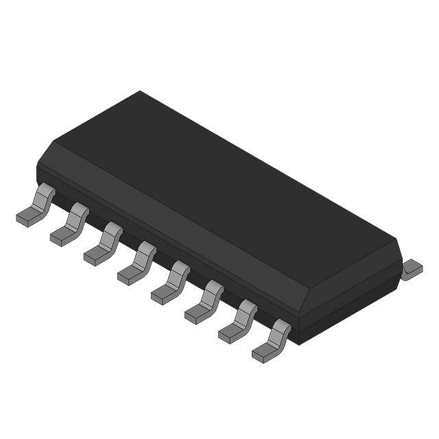
D PACKAGE
(TOP VIEW)
MIL-STD-883, Method 3015; Exceeds 50 V
Using Machine Model (C = 200 pF, R = 0)
Push-Pull CMOS Output Drives Capacitive
Loads Without Pullup Resistor,
IO = ± 8 mA
Very Low Power . . . 200 µW Typ at 5 V
Fast Response Time . . . tPLH = 2.7 µs Typ
With 5-mV Overdrive
Single Supply Operation . . . 3 V to 16 V
On-Chip ESD Protection
1OUT
2OUT
VDD
2IN −
2IN +
1IN −
1IN +
1
14
2
13
3
12
4
11
5
10
6
9
7
8
3OUT
4OUT
GND
4IN +
4IN −
3IN +
3IN −
PW PACKAGE
(TOP VIEW)
1OUT
2OUT
VDD
2IN −
2IN +
1IN −
1IN +
description/ordering information
The TLC3704 consists of four independent
micropower voltage comparators designed to
operate from a single supply and be compatible
with modern HCMOS logic systems. They are
functionally similar to the LM339 but use 1/20th
the power for similar response times. The
push-pull CMOS output stage drives capacitive
loads directly without a power-consuming pullup
resistor to achieve the stated response time.
Eliminating the pullup resistor not only reduces
power dissipation, but also saves board space
and component cost. The output stage is also fully
compatible with TTL requirements.
1
2
3
4
5
6
7
3OUT
4OUT
GND
4IN +
4IN −
3IN +
3IN −
14
13
12
11
10
9
8
symbol (each comparator)
IN +
OUT
IN −
Texas Instruments LinCMOS process offers
superior analog performance to standard CMOS
processes. Along with the standard CMOS advantages of low power without sacrificing speed, high input
impedance, and low bias currents, the LinCMOS process offers extremely stable input offset voltages with large
differential input voltages. This characteristic makes it possible to build reliable CMOS comparators.
The TLC3704Q is characterized for operation from −40°C to 125°C.
ORDERING INFORMATION†
TA
−40°C to 125°C
VIOmax
AT 25°C
5 mV
ORDERABLE
PART NUMBER
PACKAGE‡
SOIC (D)
Tape and reel
TLC3704QDRQ1
TSSOP (PW)
Tape and reel
TLC3704QPWRQ1§
TOP-SIDE
MARKING
TLC3704Q1
† For the most current package and ordering information, see the Package Option Addendum at the end of this document,
or see the TI web site at http://www.ti.com.
‡ Package drawings, thermal data, and symbolization are available at http://www.ti.com/packaging.
§ Product Preview
Please be aware that an important notice concerning availability, standard warranty, and use in critical applications of
Texas Instruments semiconductor products and disclaimers thereto appears at the end of this data sheet.
LinCMOS is a trademark of Texas Instruments Incorporated.
Copyright 2008, Texas Instruments Incorporated
���
������
��� �������!��� �" #$��%�! �" �� &$'(�#�!��� )�!%*
���)$#!" #������ !� "&%#���#�!���" &%� !+% !%��" �� �%,�" ��"!�$�%�!"
"!��)��) -�����!.* ���)$#!��� &��#%""��/ )�%" ��! �%#%""���(. ��#($)%
!%"!��/ �� �(( &����%!%�"*
POST OFFICE BOX 655303
• DALLAS, TEXAS 75265
1
���������
��
���������� ������� ������� �����������
SGLS191A − JUNE 2004 − REVISED APRIL 2008
functional block diagram (each comparator)
VDD
IN+
Differential
Input
Circuits
OUT
IN−
GND
absolute maximum ratings over operating free-air temperature range (unless otherwise noted)†
Supply voltage range, VDD (see Note 1) . . . . . . . . . . . . . . . . . . . . . . . . . . . . . . . . . . . . . . . . . . . . . −0.3 V to 18 V
Differential input voltage, VID (see Note 2) . . . . . . . . . . . . . . . . . . . . . . . . . . . . . . . . . . . . . . . . . . . . . . . . . . . ±18 V
Input voltage range, VI . . . . . . . . . . . . . . . . . . . . . . . . . . . . . . . . . . . . . . . . . . . . . . . . . . . . . . . . . . . . . . . −0.3 to VDD
Output voltage range, VO . . . . . . . . . . . . . . . . . . . . . . . . . . . . . . . . . . . . . . . . . . . . . . . . . . . . . . . . . . . . −0.3 to VDD
Input current, II . . . . . . . . . . . . . . . . . . . . . . . . . . . . . . . . . . . . . . . . . . . . . . . . . . . . . . . . . . . . . . . . . . . . . . . . . . ±5 mA
Output current, IO (each output) . . . . . . . . . . . . . . . . . . . . . . . . . . . . . . . . . . . . . . . . . . . . . . . . . . . . . . . . . . ±20 mA
Total supply current into VDD . . . . . . . . . . . . . . . . . . . . . . . . . . . . . . . . . . . . . . . . . . . . . . . . . . . . . . . . . . . . . . 40 mA
Total current out of GND . . . . . . . . . . . . . . . . . . . . . . . . . . . . . . . . . . . . . . . . . . . . . . . . . . . . . . . . . . . . . . . . . . 60 mA
Continuous total power dissipation . . . . . . . . . . . . . . . . . . . . . . . . . . . . . . . . . . . . . See Dissipation Rating Table
Operating free-air temperature range, TA: TLC3704Q . . . . . . . . . . . . . . . . . . . . . . . . . . . . . . . . . −40°C to 125°C
Storage temperature range . . . . . . . . . . . . . . . . . . . . . . . . . . . . . . . . . . . . . . . . . . . . . . . . . . . . . . . . −65°C to 150°C
Lead temperature 1,6 mm (1/16 inch) from case for 10 seconds: D package . . . . . . . . . . . . . . . . . . . . . 260°C
† Stresses beyond those listed under “absolute maximum ratings” may cause permanent damage to the device. These are stress ratings only, and
functional operation of the device at these or any other conditions beyond those indicated under “recommended operating conditions” is not
implied. Exposure to absolute-maximum-rated conditions for extended periods may affect device reliability.
NOTES: 1. All voltage values, except differential voltages, are with respect to network ground.
2. Differential voltages are at IN+ with respect to IN −.
DISSIPATION RATING TABLE
2
PACKAGE
TA ≤ 25°C
POWER RATING
DERATING FACTOR
ABOVE TA = 25°C
TA = 70°C
POWER RATING
TA = 85°C
POWER RATING
TA = 125°C
POWER RATING
D
PW
950 mW
675 mW
7.6 mW/°C
5.4 mW/°C
608 mW
432 mW
494 mW
351 mW
190 mW
135 mW
POST OFFICE BOX 655303
• DALLAS, TEXAS 75265
���������
��
���������� ������� ������� �����������
SGLS191A − JUNE 2004 − REVISED APRIL 2008
recommended operating conditions
MIN
NOM
3
5
Supply voltage, VDD
Common-mode input voltage, VIC
−0.2
High-level output current, IOH
MAX
16
V
VDD − 1.5
− 20
Low-level output current, IOL
Operating free-air temperature, TA
UNIT
− 40
V
mA
20
mA
125
°C
electrical characteristics at specified operating free-air temperature, VDD = 5 V, VIC = 0 (unless
otherwise noted)
PARAMETER
TEST CONDITIONS
VIO
Input offset voltage
VDD = 5 V to 10 V,
VIC = VICRmin, See Note 3
IIO
Input offset current
VIC = 2.5 V
TA
MIN
25°C
VICR
Common-mode input voltage
range
CMRR
kSVR
Common-mode rejection ratio
Supply-voltage rejection ratio
1.2
5
7
1
125°C
VIC = 2.5 V
5
125°C
VDD = 5 V to 10 V
VOH
High-level output voltage
VID = 1 V,
IOH = − 4 mA
VOL
Low-level output voltage
VID = −1 V,
IOH = 4 mA
IDD
Supply current (all four
comparators)
Outputs low,
No load
84
125°C
83
−40°C
83
25°C
85
125°C
85
−40°C
83
25°C
4.5
4.2
25°C
nA
dB
dB
4.7
V
210
125°C
25°C
nA
V
25°C
125°C
mV
pA
30
25°C
0 to VDD − 1
−40°C to 125°C 0 to VDD − 1.5
VIC = VICRmin
UNIT
pA
15
25°C
Input bias current
MAX
−40°C to 125°C
25°C
IIB
TYP
300
500
35
−40°C to 125°C
80
175
mV
µA
NOTE 3: The offset voltage limits given are the maximum values required to drive the output up to 4.5 V or down to 0.3 V.
POST OFFICE BOX 655303
• DALLAS, TEXAS 75265
3
���������
��
���������� ������� ������� �����������
SGLS191A − JUNE 2004 − REVISED APRIL 2008
switching characteristics, VDD = 5 V, TA = 25°C
PARAMETER
tPLH
tPHL
TEST CONDITIONS
Propagation delay time, low-to-high-level output†
Propagation delay time, high-to-low-level output†
tf
Fall time
tr
Rise time
f = 10 kHz,
CL = 50 pF
TYP
Overdrive = 2 mV
4.5
Overdrive = 5 mV
2.7
Overdrive = 10 mV
1.9
Overdrive = 20 mV
1.4
Overdrive = 40 mV
1.1
VI = 1.4-V step at IN +
Overdrive = 2 mV
1.1
Overdrive = 5 mV
2.3
Overdrive = 10 mV
1.5
Overdrive = 20 mV
0.95
Overdrive = 40 mV
0.65
VI = 1.4-V step at IN +
f = 10 kHz,
Overdrive = 50 mV
CL = 50 pF
0.15
f = 10 kHz,
CL = 50 pF
f = 10 kHz,
CL = 50 pF
Overdrive = 50 mV
† Simultaneous switching of inputs causes degradation in output response.
4
MIN
POST OFFICE BOX 655303
• DALLAS, TEXAS 75265
MAX
UNIT
µss
4
µss
50
ns
125
ns
���������
��
���������� ������� ������� �����������
SGLS191A − JUNE 2004 − REVISED APRIL 2008
PRINCIPLES OF OPERATION
LinCMOS process
The LinCMOS process is a linear polysilicon-gate CMOS process. Primarily designed for single-supply
applications, LinCMOS products facilitate the design of a wide range of high-performance analog functions from
operational amplifiers to complex mixed-mode converters.
This short guide is intended to answer the most frequently asked questions related to the quality and reliability
of LinCMOS products. Direct further questions to the nearest TI field sales office.
electrostatic discharge
CMOS circuits are prone to gate oxide breakdown when exposed to high voltages even if the exposure is only
for very short periods of time. Electrostatic discharge (ESD) is one of the most common causes of damage to
CMOS devices. It can occur when a device is handled without proper consideration for environmental
electrostatic charges, e.g., during board assembly. If a circuit in which one amplifier from a dual op amp is being
used and the unused pins are left open, high voltages tends to develop. If there is no provision for ESD
protection, these voltages may eventually punch through the gate oxide and cause the device to fail. To prevent
voltage buildup, each pin is protected by internal circuitry.
Standard ESD-protection circuits safely shunt the ESD current by providing a mechanism whereby one or more
transistors break down at voltages higher than the normal operating voltages but lower than the breakdown
voltage of the input gate. This type of protection scheme is limited by leakage currents which flow through the
shunting transistors during normal operation after an ESD voltage has occurred. Although these currents are
small, on the order of tens of nanoamps, CMOS amplifiers are often specified to draw input currents as low as
tens of picoamps.
To overcome this limitation, TI design engineers developed the patented ESD-protection circuit shown in
Figure 1. This circuit can withstand several successive 2-kV ESD pulses, while reducing or eliminating leakage
currents that may be drawn through the input pins. A more detailed discussion of the operation of the TI
ESD-protection circuit is presented on the next page.
All input and output pins on LinCMOS and Advanced LinCMOS products have associated ESD-protection
circuitry that undergoes qualification testing to withstand 2000 V discharged from a 100-pF capacitor through
a 1500-Ω resistor (human body model) and 200 V from a 100-pF capacitor with no current-limiting resistor
(charged device model). These tests simulate both operator and machine handling of devices during normal
test and assembly operations.
VDD
R1
Input
To Protected Circuit
R2
Q1
Q2
D1
D2
D3
GND
Figure 1. LinCMOS ESD-Protection Schematic
POST OFFICE BOX 655303
• DALLAS, TEXAS 75265
5
���������
��
���������� ������� ������� �����������
SGLS191A − JUNE 2004 − REVISED APRIL 2008
PRINCIPLES OF OPERATION
input protection circuit operation
Texas Instruments patented protection circuitry allows for both positive- and negative-going ESD transients.
These transients are characterized by extremely fast rise times and usually low energies, and can occur both
when the device has all pins open and when it is installed in a circuit.
positive ESD transients
Initial positive charged energy is shunted through Q1 to VSS. Q1 turns on when the voltage at the input rises
above the voltage on the VDD pin by a value equal to the VBE of Q1. The base current increases through R2
with input current as Q1 saturates. The base current through R2 forces the voltage at the drain and gate of Q2
to exceed its threshold level (VT ∼ 22 to 26 V) and turn Q2 on. The shunted input current through Q1 to VSS is
now shunted through the n-channel enhancement-type MOSFET Q2 to VSS. If the voltage on the input pin
continues to rise, the breakdown voltage of the zener diode D3 is exceeded, and all remaining energy is
dissipated in R1 and D3. The breakdown voltage of D3 is designed to be 24 to 27 V, which is well below the gateoxide voltage of the circuit to be protected.
negative ESD transients
The negative charged ESD transients are shunted directly through D1. Additional energy is dissipated in R1
and D2 as D2 becomes forward biased. The voltage seen by the protected circuit is − 0.3 V to −1 V (the forward
voltage of D1 and D2).
circuit-design considerations
LinCMOS products are being used in actual circuit environments that have input voltages that exceed the
recommended common-mode input voltage range and activate the input protection circuit. Even under normal
operation, these conditions occur during circuit power up or power down, and in many cases, when the device
is being used for a signal conditioning function. The input voltages can exceed VICR and not damage the device
only if the inputs are current limited. The recommended current limit shown on most product data sheets is
± 5 mA. Figures 2 and 3 show typical characteristics for input voltage versus input current.
Normal operation and correct output state can be expected even when the input voltage exceeds the positive
supply voltage. Again, the input current should be externally limited even though internal positive current limiting
is achieved in the input protection circuit by the action of Q1. When Q1 is on, it saturates and limits the current
to approximately 5-mA collector current by design. When saturated, Q1 base current increases with input
current. This base current is forced into the VDD pin and into the device IDD or the VDD supply through R2
producing the current limiting effects shown in Figure 2. This internal limiting lasts only as long as the input
voltage is below the VT of Q2.
When the input voltage exceeds the negative supply voltage, normal operation is affected and output voltage
states may not be correct. Also, the isolation between channels of multiple devices (duals and quads) can be
severely affected. External current limiting must be used since this current is directly shunted by D1 and D2 and
no internal limiting is achieved. If normal output voltage states are required, an external input voltage clamp is
required (see Figure 4).
6
POST OFFICE BOX 655303
• DALLAS, TEXAS 75265
���������
��
���������� ������� ������� �����������
SGLS191A − JUNE 2004 − REVISED APRIL 2008
PRINCIPLES OF OPERATION
circuit-design considerations (continued)
INPUT CURRENT
vs
INPUT VOLTAGE
INPUT CURRENT
vs
INPUT VOLTAGE
8
10
TA = 25° C
TA = 25° C
9
7
I I − Input Current − mA
I I − Input Current − mA
8
6
5
4
3
2
7
6
5
4
3
2
1
1
0
VDD
VDD + 4
VDD + 8
VDD + 12
0
VDD − 0.3
VDD − 0.5
VI − Input Voltage − V
VDD − 0.7
VDD − 0.9
VI − Input Voltage − V
Figure 2
Figure 3
VDD
RI
VI
Positive Voltage Input Current Limit :
+
1/2
TLC3704
Vref
RI +
−
V I * V DD * 0.3 V
5 mA
Negative Voltage Input Current Limit :
* V I * V DD * (* 0.3 V)
RI +
5 mA
See Note A
NOTE A: If the correct input state is required when the negative input exceeds GND, a Schottky clamp is required.
Figure 4. Typical Input Current-Limiting Configuration for a LinCMOS Comparator
POST OFFICE BOX 655303
• DALLAS, TEXAS 75265
7
���������
��
���������� ������� ������� �����������
SGLS191A − JUNE 2004 − REVISED APRIL 2008
PARAMETER MEASUREMENT INFORMATION
The TLC3704 contains a digital output stage which, if held in the linear region of the transfer curve, can cause
damage to the device. Conventional operational amplifier/comparator testing incorporates the use of a servo
loop which is designed to force the device output to a level within this linear region. Since the servo-loop method
of testing cannot be used, we offer the following alternatives for measuring parameters such as input offset
voltage, common-mode rejection, etc.
To verify that the input offset voltage falls within the limits specified, the limit value is applied to the input as shown
in Figure 5(a). With the noninverting input positive with respect to the inverting input, the output should be high.
With the input polarity reversed, the output should be low.
A similar test can be made to verify the input offset voltage at the common-mode extremes. The supply voltages
can be slewed as shown in Figure 5(b) for the VICR test, rather than changing the input voltages, to provide
greater accuracy.
5V
1V
+
Applied VIO
Limit
+
−
VO
Applied VIO
Limit
−
VO
−4V
(a) VIO WITH VIC = 0 V
(b) VIO WITH VIC = 4 V
Figure 5. Method for Verifying That Input Offset Voltage Is Within Specified Limits
A close approximation of the input offset voltage can be obtained by using a binary search method to vary the
differential input voltage while monitoring the output state. When the applied input voltage differential is equal,
but opposite in polarity, to the input offset voltage, the output changes states.
Figure 6 illustrates a practical circuit for direct dc measurement of input offset voltage that does not bias the
comparator in the linear region. The circuit consists of a switching mode servo loop in which IC1a generates
a triangular waveform of approximately 20-mV amplitude. IC1b acts as a buffer, with C2 and R4 removing any
residual d.c. offset. The signal is then applied to the inverting input of the comparator under test, while the
noninverting input is driven by the output of the integrator formed by IC1c through the voltage divider formed
by R8 and R9. The loop reaches a stable operating point when the output of the comparator under test has a
duty cycle of exactly 50%, which can only occur when the incoming triangle wave is sliced symmetrically or when
the voltage at the noninverting input exactly equals the input offset voltage.
Voltage divider R8 and R9 provides an increase in the input offset voltage by a factor of 100 to make
measurement easier. The values of R5, R7, R8, and R9 can significantly influence the accuracy of the reading;
therefore, it is suggested that their tolerance level be one percent or lower.
Measuring the extremely low values of input current requires isolation from all other sources of leakage current
and compensation for the leakage of the test socket and board. With a good picoammeter, the socket and board
leakage can be measured with no device in the socket. Subsequently, this open socket leakage value can be
subtracted from the measurement obtained with a device in the socket to obtain the actual input current of the
device.
8
POST OFFICE BOX 655303
• DALLAS, TEXAS 75265
���������
��
���������� ������� ������� �����������
SGLS191A − JUNE 2004 − REVISED APRIL 2008
PARAMETER MEASUREMENT INFORMATION
VDD
IC1a
1/4 TLC274CN
+
Buffer
C2
1 µF
R6
1 MΩ
−
C3
0.68 µF
R5
1.8 kΩ 1%
IC1c
1/4 TLC274CN
DUT
−
R4
47 kΩ
−
VIO
(X100)
+
+
R7
1.8 kΩ 1%
R1
240 kΩ
Integrator
C4
0.1 µF
IC1b
1/4 TLC274CN
−
C1
0.1 µF
+
R3
100 Ω
Triangle
Generator
R9
100 Ω 1%
R8
10 kΩ 1%
R2
10 kΩ
Figure 6. Circuit for Input Offset Voltage Measurement
Response time is defined as the interval between the application of an input step function and the instant when
the output reaches 50% of its maximum value. Response time for the low-to-high-level output is measured from
the leading edge of the input pulse, while response time for the high-to-low-level output is measured from the
trailing edge of the input pulse. Response time measurement at low input signal levels can be greatly affected
by the input offset voltage. The offset voltage should be balanced by the adjustment at the inverting input as
shown in Figure 7, so that the circuit is just at the transition point. A low signal, for example 105-mV or 5-mV
overdrive, causes the output to change state.
POST OFFICE BOX 655303
• DALLAS, TEXAS 75265
9
���������
��
���������� ������� ������� �����������
SGLS191A − JUNE 2004 − REVISED APRIL 2008
PARAMETER MEASUREMENT INFORMATION
VDD
Pulse
Generator
1 µF
50 Ω
+
1V
DUT
10 Ω
10-Turn
Potentiometer
−
1 kΩ
CL
(see Note A)
0.1 µF
−1V
TEST CIRCUIT
Overdrive
Overdrive
Input
Input
100 mV
100 mV
90%
Low-to-High
Level Output
90%
High-to-Low
Level Output
50%
10%
50%
10%
tf
tr
tPHL
tPLH
VOLTAGE WAVEFORMS
NOTE A: CL includes probe and jig capacitance.
Figure 7. Response, Rise, and Fall Times Circuit and Voltage Waveforms
10
POST OFFICE BOX 655303
• DALLAS, TEXAS 75265
���������
��
���������� ������� ������� �����������
SGLS191A − JUNE 2004 − REVISED APRIL 2008
TYPICAL CHARACTERISTICS
Table of Graphs
FIGURE
VIO
IIB
Input offset voltage
Distribution
8
Input bias current
vs Free-air temperature
9
CMRR
Common-mode rejection ratio
vs Free-air temperature
10
kSVR
Supply-voltage rejection ratio
vs Free-air temperature
11
VOH
High-level output current
vs Free-air temperature
vs High-level output current
12
13
VOL
Low-level output voltage
vs Low-level output current
vs Free-air temperature
14
15
tt
Output transition time
vs Load capacitance
16
tPLH
tPHL
IDD
Supply current response to an output voltage transition
17
Low-to-high-level output response for various input overdrives
18
High-to-low-level output response for various input overdrives
19
Low-to-high-level output response time
vs Supply voltage
20
High-to-low-level output response time
vs Supply voltage
21
Supply current
vs Frequency
vs Supply voltage
vs Free-air temperature
22
23
24
INPUT BIAS CURRENT
vs
FREE-AIR TEMPERATURE†
DISTRIBUTION OF INPUT
OFFSET VOLTAGE†
180
Number of Units
160
140
120
100
80
60
40
20
ÉÉ
ÉÉ
ÉÉÇ
ÉÉÇ
ÉÉÇ
ÉÉÇ
ÉÉÇ
Ç
ÉÉÇ
Ç
Ç
Ç
ÇÇÉÉÉ
ÉÉ
ÉÉÉÉ
ÇÇÉÇ
ÇÉ
ÉÉÇ
Ç
ÇÇÉÇ
ÉÉ
Ç
É
ÇÇÉ
ÇÇ
ÉÉÉÉ
ÇÇÉ
ÇÇÉÇ
ÇÇÇÇ
ÇÇÇÇ
ÉÉ
ÉÉ
0
−5
10
VDD = 5 V
VIC = 2.5 V
TA = 25° C
698 Units Tested
From 4 Wafer Lots
−4
−3
−2
−1
0
1
2
3
4
VDD = 5 V
VIC = 2.5 V
IIB − Input Bias Current − nA
200
1
0.1
0.01
0.001
5
25
50
75
100
125
TA − Free-Air Temperature − °C
VIO − Input Offset Voltage − mV
Figure 9
Figure 8
† Data at high and low temperatures are applicable only within the rated operating free-air temperature ranges of the various devices.
POST OFFICE BOX 655303
• DALLAS, TEXAS 75265
11
���������
��
���������� ������� ������� �����������
SGLS191A − JUNE 2004 − REVISED APRIL 2008
TYPICAL CHARACTERISTICS†
COMMON-MODE REJECTION RATIO
vs
FREE-AIR TEMPERATURE
SUPPLY VOLTAGE REJECTION RATIO
vs
FREE-AIR TEMPERATURE
88
90
k SVR − Supply Voltage Rejection Ratio − dB
CMRR − Common-Mode Rejection Ratio − dB
90
VDD = 5 V
86
84
82
80
78
76
74
72
70
−75
−50
−25
0
25
50
75
100
88
VDD = 5 V to 10 V
86
84
82
80
78
76
74
72
70
−75
125
−50
TA − Free-Air Temperature − °C
−25
Figure 10
50
75
100
VDD
VOH − High-Input Level Output Voltage −V
VDD = 5 V
IOH = − 4 mA
4.9
4.85
4.8
4.75
4.7
4.65
4.6
4.55
4.5
−75 −50
−0.25
VDD = 16 V
−0.5
−0.75
10 V
−1
5V
−1.25
4V
−1.5
−1.75
3V
TA = 25°C
−2
−25
0
25
50
75
100
125
TA − Free-Air Temperature − °C
0
−2.5
−5
−7.5
−10 −12.5 −15 −17.5 −20
IOH − High-Level Output Current − mA
Figure 12
Figure 13
† Data at high and low temperatures are applicable only within the rated operating free-air temperature ranges of the various devices.
12
125
HIGH-LEVEL OUTPUT VOLTAGE
vs
HIGH-LEVEL OUTPUT CURRENT
5
VOH − High-Level Outout Voltage − V
25
Figure 11
HIGH-LEVEL OUTPUT VOLTAGE
vs
FREE-AIR TEMPERATURE
4.95
0
TA − Free-Air Temperature − °C
POST OFFICE BOX 655303
• DALLAS, TEXAS 75265
���������
��
���������� ������� ������� �����������
SGLS191A − JUNE 2004 − REVISED APRIL 2008
TYPICAL CHARACTERISTICS†
LOW-LEVEL OUTPUT VOLTAGE
vs
LOW-LEVEL OUTPUT CURRENT
LOW-LEVEL OUTPUT VOLTAGE
vs
FREE-AIR TEMPERATURE
400
TA = 25°C
3V
VOL − Low-Level Output Voltage − mV
VOL − Low-Level Output Voltage − V
1.5
4V
1.25
1
5V
0.75
10 V
0.5
0.25
VDD = 16 V
0
0
2
4
6
8
10
12
14
16
18
VDD = 5 V
IOL = 4 mA
350
300
250
200
150
100
50
0
−75
20
−50
−25
50
75
100
125
Figure 15
Figure 14
OUTPUT TRANSITION TIME
vs
LOAD CAPACITANCE
SUPPLY CURRENT RESPONSE
TO AN OUTPUT VOLTAGE TRANSITION
250
VDD = 5 V
CL = 50 pF
f = 10 kHz
VDD = 5 V
TA = 25°C
10
IDD − Supply
Current − mA
200
Rise Time
175
150
125
Fall Time
5
0
100
75
Output
Voltage − V
tt − Transition Time − ns
25
TA − Free-Air Temperature − °C
IOL − Low-Level Output Current − mA
225
0
50
25
5
0
0
0
200
400
600
800
1000
t − Time
CL − Load Capacitance − pF
Figure 17
Figure 16
† Data at high and low temperatures are applicable only within the rated operating free-air temperature ranges of the various devices.
POST OFFICE BOX 655303
• DALLAS, TEXAS 75265
13
���������
��
���������� ������� ������� �����������
SGLS191A − JUNE 2004 − REVISED APRIL 2008
TYPICAL CHARACTERISTICS
HIGH-TO-LOW-LEVEL OUTPUT RESPONSE
FOR VARIOUS INPUT OVERDRIVES
LOW-TO-HIGH-LEVEL OUTPUT RESPONSE
FOR VARIOUS INPUT OVERDRIVES
5
5
VO − Output
Voltage − V
40 mV
20 mV
10 mV
5 mV
2 mV
0
0
100
100
Differential
Input
Voltage − mV
Differential
Input
Voltage − mV
VO − Output
Voltage − V
40 mV
20 mV
10 mV
5 mV
2 mV
VDD = 5 V
TA = 25° C
CL = 50 pF
0
0
1
2
3
4
VDD = 5 V
TA = 25° C
CL = 50 pF
0
0
5
1
2
3
4
5
tPHL − High-to-Low-Level Output
Response Time − µs
tPLH − Low-to-High-Level Output
Response Time − µs
Figure 19
Figure 18
LOW-TO-HIGH-LEVEL
OUTPUT RESPONSE TIME
vs
SUPPLY VOLTAGE
HIGH-TO-LOW-LEVEL
OUTPUT RESPONSE TIME
vs
SUPPLY VOLTAGE
6
6
CL = 50 pF
TA = 25°C
5
CL = 50 pF
TA = 25°C
5
t PHL − High-to-Low-Level
Output Response − µs
t PLH − Low-to-High-Level
Output Response − µs
Overdrive = 2 mV
4
5 mV
3
10 mV
2
20 mV
1
Overdrive = 2 mV
4
3
5 mV
2
10 mV
20 mV
1
40 mV
40 mV
0
0
2
4
6
8
10
12
14
16
0
0
VDD − Supply Voltage − V
4
6
8
Figure 21
POST OFFICE BOX 655303
10
12
VDD − Supply Voltage − V
Figure 20
14
2
• DALLAS, TEXAS 75265
14
16
���������
��
���������� ������� ������� �����������
SGLS191A − JUNE 2004 − REVISED APRIL 2008
TYPICAL CHARACTERISTICS†
AVERAGE SUPPLY CURRENT
(PER COMPARATOR)
vs
FREQUENCY
SUPPLY CURRENT
vs
SUPPLY VOLTAGE
80
TA = 25°C
CL = 50 pF
TA = − 55°C
Outputs Low
No Loads
70
TA = − 40°C
VDD = 16 V
VDD − Supply Current − µ A
VDD − Average Supply Current − µ A
10000
1000
10 V
5V
100
4V
60
TA = 25°C
50
40
30
TA = 125°C
20
TA = 85°C
10
3V
10
0.01
0.1
1
10
0
100
0
2
4
6
8
10
12
14
16
VDD − Supply Voltage − V
f − Frequency − kHz
Figure 22
Figure 23
SUPPLY CURRENT
vs
FREE-AIR TEMPERATURE
30
VDD = 5 V
No Load
IDD − Supply Current −µA
25
20
Outputs Low
15
10
Outputs High
5
0
−75
−50
−25
0
25
50
75
100
125
TA − Free-Air Temperature − °C
Figure 24
† Data at high and low temperatures are applicable only within the rated operating free-air temperature ranges of the various devices.
POST OFFICE BOX 655303
• DALLAS, TEXAS 75265
15
���������
��
���������� ������� ������� �����������
SGLS191A − JUNE 2004 − REVISED APRIL 2008
APPLICATION INFORMATION
The inputs should always remain within the supply rails in order to avoid forward biasing the diodes in the electrostatic
discharge (ESD) protection structure. If either input exceeds this range, the device is not damaged as long as the
input is limited to less than 5 mA. To maintain the expected output state, the inputs must remain within the
common-mode range. For example, at 25°C with VDD = 5 V, both inputs must remain between − 0.2 V and 4 V to
ensure proper device operation. To ensure reliable operation, the supply should be decoupled with a capacitor
(0.1 µF) that is positioned as close to the device as possible.
Output and supply current limitations should be watched carefully since the TLC3704 does not provide current
protection. For example, each output can source or sink a maximum of 20 mA; however, the total current to ground
can only be an absolute maximum of 60 mA. This prohibits sinking 20 mA from each of the four outputs simultaneously
since the total current to ground would be 80 mA.
The TLC3704 has internal ESD-protection circuits that prevents functional failures at voltages up to 2000 V as tested
under MIL-STD-883C, Method 3015.2; however, care should be exercised in handling these devices as exposure
to ESD may result in the degradation of the device parametric performance.
Table of Applications
FIGURE
16
Pulse-width-modulated motor speed controller
25
Enhanced supply supervisor
26
Two-phase nonoverlapping clock generator
27
Micropower switching regulator
28
POST OFFICE BOX 655303
• DALLAS, TEXAS 75265
���������
��
���������� ������� ������� �����������
SGLS191A − JUNE 2004 − REVISED APRIL 2008
APPLICATION INFORMATION
12 V
EN
1/2 TLC3704
See
Note A
+
100 kΩ
+
10 kΩ
5V
SN75603
Half-H Driver
DIR
5V
−
10 kΩ
Motor
C1
0.01 µF
(see Note B)
−
1/2 TLC3704
12 V
DIR
10 kΩ
5V
10 kΩ
Motor Speed Control
Potentiometer
SN75604
Half-H Driver
EN
5V
Direction
Control
S1
SPDT
NOTES: A. The recommended minimum capacitance is 10 µF to eliminate common ground switching noise.
B. Adjust C1 for change in oscillator frequency
Figure 25. Pulse-Width-Modulated Motor Speed Controller
POST OFFICE BOX 655303
• DALLAS, TEXAS 75265
17
���������
��
���������� ������� ������� �����������
SGLS191A − JUNE 2004 − REVISED APRIL 2008
APPLICATION INFORMATION
5V
12 V
12-V
Sense
3.3 kΩ
VCC
SENSE
10 kΩ
1/2 TLC3704
+
RESIN
1 kΩ
5V
TL7705A
RESET
To µP
Reset
−
REF
CT
GND
2.5 V
1 µF
CT
(see Note B)
1/2 TLC3704
+
V(UNREG)
(see Note A)
To µP Interrupt
Early Power Fail
R1
−
Monitors 5 VDC Rail
Monitors 12 VDC Rail
Early Power Fail Warning
R2
(R1 +R2)
R2
B. The value of CT determines the time delay of reset.
NOTES: A.
V (UNREG) + 2.5
Figure 26. Enhanced Supply Supervisor
18
POST OFFICE BOX 655303
• DALLAS, TEXAS 75265
���������
��
���������� ������� ������� �����������
SGLS191A − JUNE 2004 − REVISED APRIL 2008
APPLICATION INFORMATION
12 V
R1
100 kΩ
(see Note B)
12 V
12 V
−
−
1/2 TLC3704
R2
5 kΩ
(see Note C)
100 kΩ
OUT1
+
+
−
22 kΩ
100 kΩ
C1
0.01 µF
(see Note A)
100 kΩ
1/2 TLC3704
1/2 TLC3704
OUT2
+
R3
100 kΩ
(see Note B)
12 V
OUT1
OUT2
NOTES: A. Adjust C1 for a change in oscillator frequency where:
1/f = 1.85(100 kΩ)C1
B. Adjust R1 and R3 to change duty cycle
C. Adjust R2 to change deadtime
Figure 27. Two-Phase Nonoverlapping Clock Generator
POST OFFICE BOX 655303
• DALLAS, TEXAS 75265
19
���������
��
���������� ������� ������� �����������
SGLS191A − JUNE 2004 − REVISED APRIL 2008
APPLICATION INFORMATION
V + 6 V to 16 V
I
I + 0.01 mA to 0.25 mA
L
(R1 ) R2)
V + 2.5
O
R2
1/2 TLC3704
+
100 kΩ
VI
−
100 kΩ
VI
SK9504
(see Note C)
G S
VI
1/2 TLC3704
+
−
100 kΩ
D
+
C1
180 µF
(see Note A)
47 µF
Tantalum
IN5818
100 kΩ
R1
R=6Ω
L = 1 mH
(see Note D)
VO
100 kΩ
TLC271
(see Note B)
VI
470 µF
+
R2
100 kΩ
−
C2
100 pF
100 kΩ
270 kΩ
VI
LM385
2.5 V
NOTES: A. Adjust C1 for a change in oscillator frequency
B. TLC271 − Tie pin 8 to pin 7 for low bias operation
C. SK9504 − VDS = 40 V
IDS = 1 Awill
D. To achieve microampere current drive, the inductance of the circuit must be increased.
Figure 28. Micropower Switching Regulator
20
POST OFFICE BOX 655303
• DALLAS, TEXAS 75265
RL
�PACKAGE OPTION ADDENDUM
www.ti.com
10-Dec-2020
PACKAGING INFORMATION
Orderable Device
Status
(1)
Package Type Package Pins Package
Drawing
Qty
Eco Plan
(2)
Lead finish/
Ball material
MSL Peak Temp
Op Temp (°C)
Device Marking
(3)
(4/5)
(6)
TLC3704QDRG4Q1
ACTIVE
SOIC
D
14
2500
RoHS & Green
NIPDAU
Level-1-260C-UNLIM
-40 to 125
TLC3704Q1
TLC3704QDRQ1
ACTIVE
SOIC
D
14
2500
RoHS & Green
NIPDAU
Level-1-260C-UNLIM
-40 to 125
TLC3704Q1
(1)
The marketing status values are defined as follows:
ACTIVE: Product device recommended for new designs.
LIFEBUY: TI has announced that the device will be discontinued, and a lifetime-buy period is in effect.
NRND: Not recommended for new designs. Device is in production to support existing customers, but TI does not recommend using this part in a new design.
PREVIEW: Device has been announced but is not in production. Samples may or may not be available.
OBSOLETE: TI has discontinued the production of the device.
(2)
RoHS: TI defines "RoHS" to mean semiconductor products that are compliant with the current EU RoHS requirements for all 10 RoHS substances, including the requirement that RoHS substance
do not exceed 0.1% by weight in homogeneous materials. Where designed to be soldered at high temperatures, "RoHS" products are suitable for use in specified lead-free processes. TI may
reference these types of products as "Pb-Free".
RoHS Exempt: TI defines "RoHS Exempt" to mean products that contain lead but are compliant with EU RoHS pursuant to a specific EU RoHS exemption.
Green: TI defines "Green" to mean the content of Chlorine (Cl) and Bromine (Br) based flame retardants meet JS709B low halogen requirements of