�������
www.ti.com
SLAS105D − JANUARY 1995 − REVISED APRIL 2004
��
� �
���
���� �����������
�
��� ���������
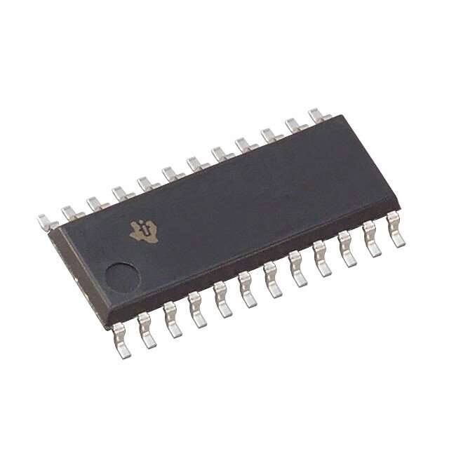
PW OR NS PACKAGE
(TOP VIEW)
features
D 8-Bit Resolution
D Differential Linearity Error
D
D
D
D
D
D
D
OE
DGND
D1(LSB)
D2
D3
D4
D5
D6
D7
D8(MSB)
VDDD
CLK
− ±0.3 LSB Typ, ±1 LSB Max (25°C)
− ±1 LSB Max
Integral Linearity Error
− ±0.6 LSB, ±0.75 LSB Max (25°C)
− ±1 LSB Max
Maximum Conversion Rate of
40 Megasamples Per Second (MSPS) Max
Internal Sample and Hold Function
5-V Single Supply Operation
Low Power Consumption . . . 85 mW Typ
Analog Input Bandwidth . . . ≥75 MHz Typ
Internal Reference Voltage Generators
1
24
2
23
3
22
4
21
5
20
6
19
7
18
8
17
9
16
10
15
11
14
12
13
DGND
REFB
REFBS
AGND
AGND
ANALOG IN
VDDA
REFT
REFTS
VDDA
VDDA
VDDD
applications
D Quadrature Amplitude Modulation (QAM)
D
D
D
D
D
D
and Quadrature Phase Shift Keying (QPSK)
Demodulators
Digital Television
Charge-Coupled Device (CCD) Scanners
Video Conferencing
Digital Set-Top Box
Digital Down Converters
High-Speed Digital Signal Processor Front
End
AVAILABLE OPTIONS
PACKAGE
TA
TSSOP (PW)
SOP (NS)
−0°C to 70°C TLC5540CPW TLC5540CNSLE
−40°C to 85°C TLC5540IPW TLC5540INSLE
description
The TLC5540 is a high-speed, 8-bit analog-to-digital converter (ADC) that converts at sampling rates up to 40
megasamples per second (MSPS). Using a semiflash architecture and CMOS process, the TLC5540 is able
to convert at high speeds while still maintaining low power consumption and cost. The analog input bandwidth
of 75 MHz (typ) makes this device an excellent choice for undersampling applications. Internal resistors are
provided to generate 2-V full-scale reference voltages from a 5-V supply, thereby reducing external
components. The digital outputs can be placed in a high impedance mode. The TLC5540 requires only a single
5-V supply for operation.
Please be aware that an important notice concerning availability, standard warranty, and use in critical applications of Texas Instruments
semiconductor products and disclaimers thereto appears at the end of this data sheet.
�������
�� ���� ����������� �� !"��#�� �� �� $"%&�!����� '��#( ���'"!��
!������ �� �$#!���!������ $#� �)# �#��� �� �#*��
����"�#��� ����'��' +������,(
���'"!���� $��!#����- '�#� ��� �#!#�����&, ��!&"'# �#����- �� �&& $����#�#��(
Copyright 1995-2004, Texas Instruments Incorporated
��������
www.ti.com
SLAS105D − JANUARY 1995 − REVISED APRIL 2004
functional block diagram
Resistor
Reference
Divider
OE
REFB
270 Ω
NOM
Lower Sampling
Comparators
(4 Bit)
REFT
REFBS
Lower Encoder
(4 Bit)
D1(LSB)
D2
Lower Data
Latch
80 Ω
NOM
D3
AGND
D4
Lower Sampling
Comparators
(4 Bit)
AGND
Lower Encoder
(4 Bit)
VDDA
D5
320 Ω
NOM
REFTS
ANALOG IN
CLK
D6
Upper Data
Latch
Upper Sampling
Comparators
(4 Bit)
D7
Upper Encoder
(4 Bit)
D8(MSB)
Clock
Generator
schematics of inputs and outputs
EQUIVALENT OF ANALOG INPUT
EQUIVALENT OF EACH DIGITAL INPUT
VDDA
AGND
VDDD
D1 −D8
OE, CLK
ANALOG IN
2
VDDD
EQUIVALENT OF EACH DIGITAL OUTPUT
DGND
DGND
��������
www.ti.com
SLAS105D − JANUARY 1995 − REVISED APRIL 2004
Terminal Functions
TERMINAL
NAME
AGND
NO.
I/O
20, 21
DESCRIPTION
Analog ground
ANALOG IN
19
I
Analog input
CLK
12
I
Clock input
DGND
2, 24
D1 −D8
3 −10
O
Digital data out. D1:LSB, D8:MSB
1
I
Output enable. When OE = L, data is enabled. When OE = H, D1−D8 is high impedance.
OE
Digital ground
VDDA
VDDD
14, 15, 18
Analog VDD
11, 13
Digital VDD
REFB
23
REFBS
22
REFT
17
REFTS
16
I
ADC reference voltage in (bottom)
Reference voltage (bottom). When using the internal voltage divider to generate a nominal 2-V reference, the
REFBS terminal is shorted to the REFB terminal and the REFTS terminal is shorted to the REFT terminal (see
Figure 13 and Figure 14).
I
Reference voltage in (top)
Reference voltage (top). When using the internal voltage divider to generate a nominal 2-V reference, the
REFTS terminal is shorted to the REFT terminal and the REFBS terminal is shorted to the REFB terminal (see
Figure 13 and Figure 14).
absolute maximum ratings over operating free-air temperature range (unless otherwise noted)†
Supply voltage, VDDA, VDDD . . . . . . . . . . . . . . . . . . . . . . . . . . . . . . . . . . . . . . . . . . . . . . . . . . . . . . . . . . . . . . . . . 7 V
Reference voltage input range, VI(REFT), VI(REFB), VI(REFBS), VI(REFTS) . . . . . . . . . . . . . . . . AGND to VDDA
Analog input voltage range, VI(ANLG) . . . . . . . . . . . . . . . . . . . . . . . . . . . . . . . . . . . . . . . . . . . . . . . AGND to VDDA
Digital input voltage range, VI(DGTL) . . . . . . . . . . . . . . . . . . . . . . . . . . . . . . . . . . . . . . . . . . . . . . . . DGND to VDDD
Digital output voltage range, VO(DGTL) . . . . . . . . . . . . . . . . . . . . . . . . . . . . . . . . . . . . . . . . . . . . . . DGND to VDDD
Operating free-air temperature range, TA: TLC5540C . . . . . . . . . . . . . . . . . . . . . . . . . . . . . . . . . . . . 0°C to 70°C
TLC5540I . . . . . . . . . . . . . . . . . . . . . . . . . . . . . . . . . . . . . . . . . . . . . . . . . . . . . . . . . . . . . . . . . . . . . . . . −40°C to 85°C
Storage temperature range, Tstg . . . . . . . . . . . . . . . . . . . . . . . . . . . . . . . . . . . . . . . . . . . . . . . . . . . −55°C to 150°C
† Stresses beyond those listed under “absolute maximum ratings” may cause permanent damage to the device. These are stress ratings only, and
functional operation of the device at these or any other conditions beyond those indicated under “recommended operating conditions” is not implied.
Exposure to absolute-maximum-rated conditions for extended periods may affect device reliability.
3
��������
www.ti.com
SLAS105D − JANUARY 1995 − REVISED APRIL 2004
recommended operating conditions
Supply voltage
MIN
NOM
MAX
VDDA −AGND
VDDD −AGND
4.75
5
5.25
4.75
5
5.25
AGND −DGND
−100
0
100
Reference input voltage (top), VI(REFT)
VI(REFB)+1.8
0
Reference input voltage (bottom), VI(REFB)
Analog input voltage range, VI(ANLG) (see Note 1)
Full scale voltage, VI(REFT) − VI(REFB)
High-level input voltage, VIH
VI(REFB)
1.8
VI(REFB)+2
0.6
VDDA
VI(REFT)−1.8
VI(REFT)
5
4
Low-level input voltage, VIL
UNIT
V
mV
V
V
V
V
V
1
V
Pulse duration, clock high, tw(H)
12.5
ns
Pulse duration, clock low, tw(L)
12.5
ns
TLC5540C
Operating free-air temperature, TA
(1)
4
TLC5540I
1.8 V ≤ VI(REFT) − VI(REFB) < VDD
0
70
°C
−40
85
°C
��������
www.ti.com
SLAS105D − JANUARY 1995 − REVISED APRIL 2004
electrical characteristics at VDD = 5 V, VI(REFT) = 2.6 V, VI(REFB) = 0.6 V, fs = 40 MSPS, TA = 25°C
(unless otherwise noted)
TEST CONDITIONS†
PARAMETER
EL
ED
Linearity error, integral
Linearity error, differential
fs = 40 MSPS,
VI = 0.6 V to 2.6 V
Self bias (1), VRB
Short REFB to REFBS
Self bias (1), VRT
Short REFT to REFTS
Self bias (2), VRB
Short REFB to AGND
TYP
MAX
TA = 25°C
TA = MIN to MAX
MIN
± 0.6
±1
TA = 25°C
TA = MIN to MAX
± 0.3
± 0.75
See Figure 13
See Figure 14
Self bias (2), VRT
Short REFT to REFTS
Reference-voltage current
Reference-voltage resistor
VI(REFT) − VI(REFB) = 2 V
Between REFT and REFB terminals
Ci
EZS
Analog input capacitance
VI(ANLG) = 1.5 V + 0.07 Vrms
0.57
0.61
0.65
2.47
2.63
2.80
V
EFS
IIH
Full-scale error
IIL
IOH
Low-level input current
VDD = 5.25 V,
VDD = 5.25 V,
VIH = VDD
VIL = 0
High-level output current
OE = GND,
IOL
Low-level output current
OE = GND,
VDD = 4.75 V,
VDD = 4.75 V,
VOH = VDD −0.5 V
VOL = 0.4 V
IOZH(lkg)
High-level
high-impedance-state
output leakage current
OE = VDD,
VDD = 5.25,
VOH = VDD
IOZL(lkg)
Low-level
high-impedance-state
output leakage current
OE = VDD,
IDD
Supply current
fs = 40 MSPS, CL ≤ 25 pF,
NTSC‡ ramp wave input, See Note 1
2.18
2.29
2.4
5.2
7.5
12
165
270
350
4
Zero-scale error
VI(REFT) − VI(REFB) = 2 V
LSB
±1
AGND
Iref
Rref
High-level input current
±1
UNIT
mA
Ω
pF
−18
−43
−68
−25
0
25
5
5
mV
µA
A
−1.5
mA
2.5
16
µA
A
VDD = 4.75,
VOL = 0
16
17
27
mA
† Conditions marked MIN or MAX are as stated in recommended
operating conditions.
‡ National Television System Committee
(1) Supply current specification does not include Iref.
5
��������
www.ti.com
SLAS105D − JANUARY 1995 − REVISED APRIL 2004
operating characteristics at VDD = 5 V, VRT = 2.6 V, VRB = 0.6 V, fs = 40 MSPS, TA = 25°C (unless
otherwise noted)
PARAMETER
TEST CONDITIONS†
fs
fs
Maximum conversion rate
Minimum conversion rate
TA = MIN to MAX
TA = MIN to MAX
BW
Analog input full-power bandwidth
At − 3 dB,
tpd
tPHZ
Delay time, digital output
tPLZ
tPZH
Disable time, output low to Hi-Z
tPZL
Enable time, Hi-Z to output low
Disable time, output high to Hi-Z
Enable time, Hi-Z to output high
Differential gain
Differential phase
tAJ
td(s)
5
9
MHz
15
ns
20
ns
20
ns
CL ≤ 15 pF,
CL ≤ 15 pF,
IOH = − 4.5 mA
IOL = 5 mA
15
ns
15
ns
1%
NTSC 40 IRE‡ modulation wave,
fs = 14.3 MSPS
Sampling delay time
Signal-to-noise ratio
fs = 20 MSPS
Effective number of bits
fs = 40 MSPS
fs = 20 MSPS
Total harmonic distortion
fs = 40 MSPS
fs = 20 MSPS
fs = 40 MSPS
† Conditions marked MIN or MAX are as stated in recommended operating conditions.
‡ Institute of Radio Engineers
(2) CL includes probe and jig capacitance.
6
MSPS
IOH = − 4.5 mA
IOL = 5 mA
Aperture jitter time
Spurious-free dynamic range
UNIT
MSPS
75
fI = 1 MHz
fI = 3 MHz
44
fI = 6 MHz
fI = 10 MHz
fI = 3 MHz
fI = 6 MHz
0.7
degrees
30
ps
4
ns
47
47
46
45
42
44
42
7.64
fI = 3 MHz
fI = 6 MHz
7.61
fI = 10 MHz
fI = 3 MHz
7.16
fI = 6 MHz
fI = 1 MHz
6.8
fI = 3 MHz
fI = 6 MHz
7.47
Bits
7
43
35
42
41
fI = 10 MHz
fI = 3 MHz
38
dBc
40
fI = 6 MHz
38
41
fI = 3 MHz
dB
45.2
fI = 10 MHz
fI = 1 MHz
THD
MAX
CL ≤ 15 pF,
CL ≤ 15 pF,
fs = 40 MSPS
ENOB
TYP
40
VI(ANLG) = 2 Vpp
CL ≤ 10 pF (see Note 2)
fs = 20 MSPS
SNR
MIN
46
42
dBc
��������
www.ti.com
SLAS105D − JANUARY 1995 − REVISED APRIL 2004
PARAMETER MEASUREMENT INFORMATION
tw(H)
tw(L)
CLK (Clock)
ANALOG IN
(Input Signal)
D1 −D8
(Output Data)
N+2
N+1
N
N+4
N+3
N −3
N −2
N −1
N
N+1
tpd
Figure 1. I/O Timing Diagram
Reference Level
(2.5 V)
OE
Data Output
Active
tPHZ
tPLZ
Hi-Z
VOH (4.5 V typical)
Active
tPZH
tPZL
VOL (0.4 V typical)
Figure 2. I/O Timing Diagram
7
��������
www.ti.com
SLAS105D − JANUARY 1995 − REVISED APRIL 2004
TYPICAL CHARACTERISTICS
POWER DISSIPATION
vs
SAMPLING FREQUENCY
ANALOG INPUT BANDWIDTH
0.5
200
VDD = 5 V
TA = 25°C
0
150
−1
−1.5
Gain − dB
Power Dissipation − mW
−0.5
100
−2
−2.5
−3
−3.5
50
−4
−4.5
−5
0.1
0
0
5
25
30
35
10
20
15
fs − Sampling Frequency − MHz
40
VCC = 5 V, VRT = 2.6 V, VRB = 0.6 V
CLK = 40 MHz
ANALOG IN = 100 k − 100 MHz Sine Wave
VI = 2 V(PP)
1
10
fI − Input Frequency − MHz
Figure 3
Figure 4
SIGNAL-TO-NOISE RATIO
vs
INPUT FREQUENCY
EFFECTIVE NUMBER OF BITS
vs
INPUT FREQUENCY
8
50
7
fs = 40 MHz
6
5
4
3
2
VDD = 5 V, VI = 1 V(PP)
VRB = 2.6 V, VRT = 0.6 V
1
0
5
10
fI − Input Frequency − MHz
Figure 5
8
fs = 20 MHz
45
SNR − Signal-to-Noise Ratio − dB
ENOB − Effective Number of Bits − BITS
fs = 20 MHz
0
100
fs = 40 MHz
40
35
30
25
20
15
10
VDD = 5 V, VI = 1 V(PP)
VRB = 2.6 V, VRT = 0.6 V
5
15
0
0
5
10
fI − Input Frequency − MHz
Figure 6
15
��������
www.ti.com
SLAS105D − JANUARY 1995 − REVISED APRIL 2004
TYPICAL CHARACTERISTICS
EFFECTIVE NUMBER OF BITS
vs
AMBIENT TEMPERATURE
DIFFERENTIAL NONLINEARITY
8
1
0.6
ENOB − Effective Number of Bits − BITS
Differential Nonlinearity − LSB
0.8
VI = Vramp = 0.6 V − 2.6 V, 500 Hz
VRT = 2.6 V, VRB = 0.6 V, VDD = 5 V
fs = 40 MHz
TA = 25°C
0.4
0.2
0
−0.2
−0.4
−0.6
−0.8
−1
0
40
80
120
160
200
VDD = 5 V, VI = 1 V(PP), 3 MHz Sine Wave
VRT = 2.6 V, VRB = 0.6 V, fs = 20 MHz
7.5
7
6.5
6
−40
240
0
−20
20
Figure 7
INTEGRAL NONLINEARITY
FFT SPECTRUM
VI = Vramp = 0.6 V − 2.6 V, 500 Hz
VRT = 2.6 V, VRB = 0.6 V, VDD = 5 V
fs = 40 MHz, TA = 25°C
VI = 2 V(PP), 1 MHz Sine Wave
VRT = 2.6 V, VRB = 0.6 V
fs = 20 MHz, TA = 25°C
−10
−20
−30
Magnitude − dB
Integral Nonlinearity − LSB
100
0
0.4
0.2
0
−0.2
−40
−50
−60
−0.4
−70
−0.6
−80
−0.8
−90
−1
0
80
Figure 8
1
0.6
60
TA − Ambient Temperature − °C
Digital Output Code
0.8
40
−100
40
80
120
160
Digital Output Code
Figure 9
200
240
0
1
2
3
4
5
6
7
8
9
10
f − Frequency − MHz
Figure 10
9
��������
www.ti.com
SLAS105D − JANUARY 1995 − REVISED APRIL 2004
APPLICATION INFORMATION
grounding and power supply considerations
A signal ground is a low-impedance path for current to return to the source. Inside the TLC5540 A/D converter,
the analog ground and digital ground are connected to each other through the substrate, which has a very small
resistance (~30 Ω) to prevent internal latch-up. For this reason, it is strongly recommended that a printed circuit
board (PCB) of at least 4 layers be used with the TLC5540 and the converter DGND and AGND pins be
connected directly to the analog ground plane to avoid a ground loop. Figure 11 shows the recommended
decoupling and grounding scheme for laying out a multilayer PC board with the TLC5540. This scheme ensures
that the impedance connection between AGND and DGND is minimized so that their potential difference is
negligible and noise source caused by digital switching current is eliminated.
TLC5540
VDDD
11
0.1 µF
13
0.1 µF
GND
24
2
14
0.1 µF
VDDA
15
0.1 µF
18
AGND
20 21
0.1 µF
Signal Plane
Analog Ground Plane
Digital Supply Plane
Analog Supply Plane
Signal Plane
Figure 11. AVDD, DVDD, AGND, and DGND Connections
printed circuit board (PCB) layout considerations
When designing a circuit that includes high-speed digital and precision analog signals such as a high speed
ADC, PCB layout is a key component to achieving the desired performance. The following recommendations
should be considered during the prototyping and PCB design phase:
D Separate analog and digital circuitry physically to help eliminate capacitive coupling and crosstalk. When
separate analog and digital ground planes are used, the digital ground and power planes should be several
layers from the analog signals and power plane to avoid capacitive coupling.
D Full ground planes should be used. Do not use individual etches to return analog and digital currents or
partial ground planes. For prototyping, breadboards should be constructed with copper clad boards to
maximize ground plane.
D The conversion clock, CLK, should be terminated properly to reduce overshoot and ringing. Any jitter on
the conversion clock degrades ADC performance. A high-speed CMOS buffer such as a 74ACT04 or
74AC04 positioned close to the CLK terminal can improve performance.
D Minimize all etch runs as much as possible by placing components very close together. It also proves
beneficial to place the ADC in a corner of the PCB nearest to the I/O connector analog terminals.
D It is recommended to place the digital output data latch (if used) as close to the TLC5540 as possible to
minimize capacitive loading. If D0 through D7 must drive large capacitive loads, internal ADC noise may
be experienced.
10
��������
www.ti.com
SLAS105D − JANUARY 1995 − REVISED APRIL 2004
PRINCIPLES OF OPERATION
functional description
The TLC5540 uses a modified semiflash architecture as shown in the functional block diagram. The four most
significant bits (MSBs) of every output conversion result are produced by the upper comparator block CB1. The
four least significant bits (LSBs) of each alternate output conversion result are produced by the lower
comparator blocks CB-A and CB-B in turn (see Figure 12).
The reference voltage that is applied to the lower comparator resistor string is one sixteenth of the amplitude
of the refence applied to the upper comparator resistor string. The sampling comparators of the lower
comparator block require more time to sample the lower voltages of the reference and residual input voltage.
By applying the residual input voltage to alternate lower comparator blocks, each comparator block has twice
as much time to sample and convert as would be the case if only one lower comparator block were used.
VI(1)
VI(2)
VI(3)
VI(4)
ANALOG IN
(Sampling Points)
CLK1
CLK2
CLK3
CLK4
CLK (Clock)
Upper Comparators Block (CB1)
S(1)
C(1)
S(2)
C(2)
S(3)
C(3)
S(4)
C(4)
Upper Data
UD(0)
UD(1)
UD(2)
UD(3)
Lower Reference Voltage
RV(0)
RV(1)
RV(2)
RV(3)
S(1)
Lower Comparators Block (CB-A)
Lower Data (B)
C(1)
S(3)
H(3)
LD(−1)
Lower Data (A)
Lower Comparators Block (CB-B)
H(1)
H(0)
C(0)
S(2)
LD(1)
H(2)
C(2)
LD(0)
LD(−2)
C(3)
S(4)
H(4)
LD(2)
tpd
D1 −D8 (Data Output)
OUT(−2)
OUT(−1)
OUT(0)
OUT(1)
Figure 12. Internal Functional Timing Diagram
This conversion scheme, which reduces the required sampling comparators by 30 percent compared to
standard semiflash architectures, achieves significantly higher sample rates than the conventional semiflash
conversion method.
11
��������
www.ti.com
SLAS105D − JANUARY 1995 − REVISED APRIL 2004
PRINCIPLES OF OPERATION
functional description (continued)
The MSB comparator block converts on the falling edge of each applied clock cycle. The LSB comparator blocks
CB-A and CB-B convert on the falling edges of the first and second following clock cycles, respectively. The
timing diagram of the conversion algorithm is shown in Figure 12.
analog input operation
The analog input stage to the TLC5540 is a chopper-stabilized comparator and is equivalently shown below:
φ2
S2
φ1
To Encoder Logic
VDDA
Cs
φ2
S3
φ1
φ1
ANALOG IN
S1
Vref(N)
To Encoder Logic
φ2
Cs
φ2
S(N)
φ1
To Encoder Logic
Cs
Figure 13. External Connections for Using the Internal Reference Resistor Divider
Figure 13 depicts the analog input for the TLC5540. The switches shown are controlled by two internal clocks,
φ1 and φ2. These are nonoverlapping clocks that are generated from the CLK input. During the sampling period,
φ1, S1 is closed and the input signal is applied to one side of the sampling capacitor, Cs. Also during the sampling
period, S2 through S(N) are closed. This sets the comparator input to approximately 2.5 V. The delta voltage
is developed across Cs. During the comparison phase, φ2, S1 is switched to the appropriate reference voltage
for the bit value N. S2 is opened and Vref(N) − VCs toggles the comparator output to the appropriate digital 1 or
0. The small resistance values for the switch, S1, and small value of the sampling capacitor combine to produce
the wide analog input bandwidth of the TLC5540. The source impedance driving the analog input of the
TLC5540 should be less than 100 Ω across the range of input frequency spectrum.
reference inputs − REFB, REFT, REFBS, REFTS
The range of analog inputs that can be converted are determined by REFB and REFT, REFT being the
maximum reference voltage and REFB being the minimum reference voltage. The TLC5540 is tested with
REFT = 2.6 V and REFB = 0.6 V producing a 2-V full-scale range. The TLC5540 can operate with
REFT − REFB = 5 V, but the power dissipation in the reference resistor increases significantly (93 mW
nominally). It is recommended that a 0.1 µF capacitor be attached to REFB and REFT whether using externally
or internally generated voltages.
12
��������
www.ti.com
SLAS105D − JANUARY 1995 − REVISED APRIL 2004
PRINCIPLES OF OPERATION
internal reference voltage conversion
Three internal resistors allow the device to generate an internal reference voltage. These resistors are brought
out on terminals VDDA, REFTS, REFT, REFB, REFBS, and AGND. Two different bias voltages are possible
without the use of external resistors.
Internal resistors are provided to develop REFT = 2.6 V and REFB = 0.6 V (bias option one) with only two
external connections. This is developed with a 3-resistor network connected to VDDA. When using this feature,
connect REFT to REFTS and connect REFB to REFBS. For applications where the variance associated with
VDDA is acceptable, this internal voltage reference saves space and cost (see Figure 14).
A second internal bias option (bias two option) is shown in Figure 15. Using this scheme REFB = AGND and
REFT = 2.28 V nominal. These bias voltage options can be used to provide the values listed in the following
table.
Table 1. Bias Voltage Options
BIAS VOLTAGE
BIAS OPTION
1
VRB
0.61
VRT
2.63
VRT − VRB
2.02
2
AGND
2.28
2.28
To use the internally-generated reference voltage, terminal connections should be made as shown in
Figure 14 or Figure 15. The connections in Figure 14 provide the standard video 2-V reference.
TLC5540
VDDA
5 V (Analog)
REFTS
18
R1
320 Ω NOM
16
17
0.1 µF
REFT
REFB
2.63 V dc
Rref
270 Ω NOM
23
0.61 V dc
22
0.1 µF
REFBS
AGND
21
R2
80 Ω NOM
Figure 14. External Connections Using the Internal Bias One Option
13
��������
www.ti.com
SLAS105D − JANUARY 1995 − REVISED APRIL 2004
PRINCIPLES OF OPERATION
TLC5540
18
VDDA
5 V (Analog)
R1
320 Ω NOM
REFTS
16
17
0.1 µF
2.28 V dc
REFT
Rref
270 Ω NOM
REFB
23
0 V dc
22
REFBS
AGND
R2
80 Ω NOM
21
Figure 15. External Connections Using the Internal Bias Two Option
functional operation
Table 2 shows the TLC5540 functions.
Table 2. Functional Operation
14
DIGITAL OUTPUT CODE
INPUT SIGNAL
VOLTAGE
STEP
Vref(T)
255
1
1
1
1
1
1
1
1
•
•
•
•
•
•
•
•
•
•
•
•
•
•
•
•
•
•
•
•
•
128
1
0
0
0
0
0
0
0
•
127
0
1
1
1
1
1
1
1
•
•
•
•
•
•
•
•
•
•
MSB
LSB
•
•
•
•
•
•
•
•
•
•
Vref(B)
0
0
0
0
0
0
0
0
0
�PACKAGE OPTION ADDENDUM
www.ti.com
10-Dec-2020
PACKAGING INFORMATION
Orderable Device
Status
(1)
Package Type Package Pins Package
Drawing
Qty
Eco Plan
(2)
Lead finish/
Ball material
MSL Peak Temp
Op Temp (°C)
Device Marking
(3)
(4/5)
(6)
TLC5540CPW
ACTIVE
TSSOP
PW
24
60
RoHS & Green
NIPDAU
Level-2-260C-1 YEAR
0 to 70
P5540
TLC5540INSR
ACTIVE
SO
NS
24
2000
RoHS & Green
NIPDAU
Level-1-260C-UNLIM
-40 to 85
TLC5540I
TLC5540IPW
ACTIVE
TSSOP
PW
24
60
RoHS & Green
NIPDAU
Level-2-260C-1 YEAR
-40 to 85
Y5540
TLC5540IPWR
ACTIVE
TSSOP
PW
24
2000
RoHS & Green
NIPDAU
Level-2-260C-1 YEAR
-40 to 85
Y5540
(1)
The marketing status values are defined as follows:
ACTIVE: Product device recommended for new designs.
LIFEBUY: TI has announced that the device will be discontinued, and a lifetime-buy period is in effect.
NRND: Not recommended for new designs. Device is in production to support existing customers, but TI does not recommend using this part in a new design.
PREVIEW: Device has been announced but is not in production. Samples may or may not be available.
OBSOLETE: TI has discontinued the production of the device.
(2)
RoHS: TI defines "RoHS" to mean semiconductor products that are compliant with the current EU RoHS requirements for all 10 RoHS substances, including the requirement that RoHS substance
do not exceed 0.1% by weight in homogeneous materials. Where designed to be soldered at high temperatures, "RoHS" products are suitable for use in specified lead-free processes. TI may
reference these types of products as "Pb-Free".
RoHS Exempt: TI defines "RoHS Exempt" to mean products that contain lead but are compliant with EU RoHS pursuant to a specific EU RoHS exemption.
Green: TI defines "Green" to mean the content of Chlorine (Cl) and Bromine (Br) based flame retardants meet JS709B low halogen requirements of


 工商网监
湘ICP备2023018690号
工商网监
湘ICP备2023018690号
