TLC5920
16x8 BIT LED DRIVER/CONTROLLER
SLAS264A – MARCH 2000 REVISED SEPTEMBER 2002
D
D
D
D
D
D
D
D
D
D
Drive Capability:
– Segment . . . 30 mA × 16 Bits
– Common . . . 640 mA
Constant Current Output . . . 3 mA to 30 mA
(Current Value Setting for All Channels
Using External Resistor)
Constant Current Accuracy ±6% (Maximum
Error Between Bits)
Data Input: Clock Synchronized Serial Input
LED Type Applied Cathode Common
Logic Power Supply Voltage 4.5 V to 5.5 V
LED Power Supply Voltage 4.5 V to 5.5 V
Operating Frequency . . . 10 MHz
Operating Free-Air Temperature Range
–20°C to 85°C
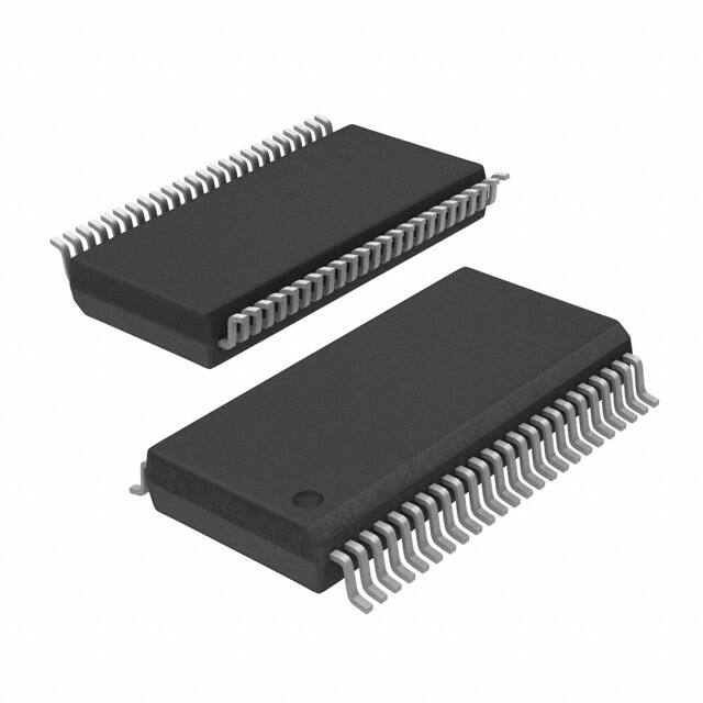
48-Pin SSOL Package
description
The TLC5920 is an LED driver incorporating a
16-channel shift register, data latch, and constant
current circuitry with current value control and
8-channel common driver into a single chip. The
constant output current is capable of 30 mA for 16
bits simultaneously, and the current value can be
set by one external register. This device also
includes a 16-bit segment driver and 8-bit
common driver; therefore, the monocolor LED
array with 16 × 8 dots can be driven by only one
TLC5920, and a two-color LED array with 16 x 16
dots can be driven by two TLC5920s.
DL PACKAGE
(TOP VIEW)
COM3
COM2
COM1
COM0
GNDLED
NC
NC
VLED
S0
S1
S2
S3
S4
S5
S6
S7
IREF
VLED
VANA
NC
GNDANA
S8
S9
S10
1
48
2
47
3
46
4
45
5
44
6
43
7
42
8
41
9
40
10
39
11
38
12
37
13
36
14
35
15
34
16
33
17
32
18
31
19
30
20
29
21
28
22
27
23
26
24
25
GNDLED
COM4
COM5
COM6
COM7
GNDLED
SIN
LATCH
SCLK
BLANK
CSEL0
GNDLOG
CSEL1
CSEL2
VLOG
DSEL
SOUT
VLED
DSEL
S15
S14
S13
S12
S11
Please be aware that an important notice concerning availability, standard warranty, and use in critical applications of
Texas Instruments semiconductor products and disclaimers thereto appears at the end of this data sheet.
Copyright 2002, Texas Instruments Incorporated
PRODUCTION DATA information is current as of publication date.
Products conform to specifications per the terms of Texas Instruments
standard warranty. Production processing does not necessarily include
testing of all parameters.
POST OFFICE BOX 655303
• DALLAS, TEXAS 75265
1
�TLC5920
16x8 BIT LED DRIVER/CONTROLLER
SLAS264A – MARCH 2000 REVISED SEPTEMBER 2002
functional block diagram
DSEL
DSEL
BLANK
COM0
CSEL0
CSEL1
3 TO 8
Decoder
Common
Driver
COM7
CSEL2
SIN
16 bits
Shift Register
SCLK
16 bits
Data Latch
LATCH
Segment Driver
and
Current Control
IREF
S0
2
SOUT
POST OFFICE BOX 655303
S15
• DALLAS, TEXAS 75265
�TLC5920
16x8 BIT LED DRIVER/CONTROLLER
SLAS264A – MARCH 2000 REVISED SEPTEMBER 2002
Terminal Functions
ÁÁÁÁÁÁÁÁÁÁÁÁÁÁÁÁÁÁÁÁÁÁÁÁÁÁÁÁÁÁÁÁÁÁÁÁ
ÁÁÁÁÁ
ÁÁÁÁÁÁ
ÁÁÁ
ÁÁÁÁÁÁÁÁÁÁÁÁÁÁÁÁÁÁÁÁÁÁ
ÁÁÁÁÁÁÁÁÁÁÁÁÁÁ
ÁÁÁÁÁÁÁÁÁÁÁÁÁÁÁÁÁÁÁÁÁÁ
ÁÁÁÁÁÁÁÁÁÁÁ
ÁÁÁÁÁÁÁÁÁ
ÁÁÁ
ÁÁÁÁÁÁÁÁÁÁÁÁÁÁÁÁÁÁÁÁÁÁ
ÁÁÁÁÁ
ÁÁÁÁÁÁÁÁÁÁÁÁÁÁÁÁÁÁÁÁÁÁ
ÁÁÁÁÁ
ÁÁÁÁÁÁ
ÁÁÁ
ÁÁÁÁÁÁÁÁÁÁÁÁÁÁÁÁÁÁÁÁÁÁ
ÁÁÁÁÁ
ÁÁÁÁÁÁ
ÁÁÁ
ÁÁÁÁÁÁÁÁÁÁÁÁÁÁÁÁÁÁÁÁÁÁ
ÁÁÁÁÁ
ÁÁÁÁÁÁ
ÁÁÁ
ÁÁÁÁÁÁÁÁÁÁÁÁÁÁÁÁÁÁÁÁÁÁ
ÁÁÁÁÁ
ÁÁÁÁÁÁ
ÁÁÁ
ÁÁÁÁÁÁÁÁÁÁÁÁÁÁÁÁÁÁÁÁÁÁ
ÁÁÁÁÁ
ÁÁÁÁÁÁ
ÁÁÁ
ÁÁÁÁÁÁÁÁÁÁÁÁÁÁÁÁÁÁÁÁÁÁ
ÁÁÁÁÁÁÁÁÁÁÁÁÁÁ
ÁÁÁÁÁÁÁÁÁÁÁÁÁÁÁÁÁÁÁÁÁÁ
ÁÁÁÁÁ
ÁÁÁÁÁÁ
ÁÁÁ
ÁÁÁÁÁÁÁÁÁÁÁÁÁÁÁÁÁÁÁÁÁÁ
ÁÁÁÁÁÁÁÁÁÁÁÁÁÁ
ÁÁÁÁÁÁÁÁÁÁÁÁÁÁÁÁÁÁÁÁÁÁ
ÁÁÁÁÁÁÁÁÁÁÁÁÁÁÁÁÁÁÁÁÁÁÁÁÁÁÁÁÁÁÁÁÁÁÁÁ
ÁÁÁÁÁÁÁÁÁÁÁÁÁÁÁÁÁÁÁÁÁÁÁÁÁÁÁÁÁÁÁÁÁÁÁÁ
ÁÁÁÁÁÁÁÁÁÁÁÁÁÁÁÁÁÁÁÁÁÁÁÁÁÁÁÁÁÁÁÁÁÁÁÁ
ÁÁÁÁÁÁÁÁÁÁÁÁÁÁÁÁÁÁÁÁÁÁ
ÁÁÁÁÁÁÁÁÁÁÁ
ÁÁÁÁÁÁÁÁÁ
ÁÁÁ
ÁÁÁÁÁÁÁÁÁÁÁÁÁÁÁÁÁÁÁÁÁÁ
ÁÁÁÁÁ
ÁÁÁÁÁÁÁÁÁÁÁÁÁÁÁÁÁÁÁÁÁÁ
ÁÁÁÁÁ
ÁÁÁÁÁÁ
ÁÁÁ
ÁÁÁÁÁÁÁÁÁÁÁÁÁÁÁÁÁÁÁÁÁÁ
ÁÁÁÁÁÁÁÁÁÁÁÁÁÁ
ÁÁÁÁÁÁÁÁÁÁÁÁÁÁÁÁÁÁÁÁÁÁ
ÁÁÁÁÁÁÁÁÁÁÁÁÁÁÁÁÁÁÁÁÁÁÁÁÁÁÁÁÁÁÁÁÁÁÁÁ
ÁÁÁÁÁ
ÁÁÁÁÁÁ
ÁÁÁ
ÁÁÁÁÁÁÁÁÁÁÁÁÁÁÁÁÁÁÁÁÁÁ
ÁÁÁÁÁÁÁÁÁÁÁÁÁÁ
ÁÁÁÁÁÁÁÁÁÁÁÁÁÁÁÁÁÁÁÁÁÁ
ÁÁÁÁÁ
ÁÁÁÁÁÁ
ÁÁÁ
ÁÁÁÁÁÁÁÁÁÁÁÁÁÁÁÁÁÁÁÁÁÁ
ÁÁÁÁÁÁÁÁÁÁÁÁÁÁ
ÁÁÁÁÁÁÁÁÁÁÁÁÁÁÁÁÁÁÁÁÁÁ
ÁÁÁÁÁÁÁÁÁÁÁÁÁÁÁÁÁÁÁÁÁÁÁÁÁÁÁÁÁÁÁÁÁÁÁÁ
ÁÁÁÁÁÁÁÁÁÁÁÁÁÁÁÁÁÁÁÁÁÁÁÁÁÁÁÁÁÁÁÁÁÁÁÁ
ÁÁÁÁÁÁÁÁÁÁÁÁÁÁÁÁÁÁÁÁÁÁÁÁÁÁÁÁÁÁÁÁÁÁÁÁ
TERMINAL
I/O
DESCRIPTION
39
I
Blank(light off). By turning all the output for the common driver off, the LED is turned off. When
BLANK is high, the LED is turned off.
4, 3, 2, 1, 47, 46,
45, 44
O
LED common driver output
38, 36, 35
I
Common driver select. One terminal out of COM0 through COM7 is selected.
2
1
0
Common Driver
L
L
L
0
L
L
H
1
L
H
L
2
L
H
H
3
H
L
L
4
H
L
H
5
H
H
L
6
H
H
H
7
DSEL
33
I
Display select. When DSEL is high, the LED is turned off. Note that, when BLANK is high,
the LED is turned off with no regard to the DSEL input.
DSEL
30
O
Display select output. The inverted data of DSEL is clocked out.
NAME
BLANK
COM0 – COM7
CSEL0 – 2
NO.
GNDANA
21
GNDLED
5, 43, 48
GNDLOG
37
IREF
17
I
Constant current control setting. The LED current is set to the desired value by connecting
an external resistor between IREF and GND.
LATCH
41
I
Latch. When LATCH is high, data on the shift register goes through latch. When LATCH is
low, data is latched.
SIN
42
I
Serial input for display
SOUT
32
O
Serial output for display
SCLK
40
I
Synchronous clock input for serial data transfer. The input data of SIN is synchronized to
the rising edge of SCLK, and transferred to SOUT.
9, 10, 11, 12, 13, 14,
15, 16, 22, 23, 24,
25, 26, 27, 28, 29
O
LED segment driver output
S0 – S15
VANA
Analog ground
LED driver ground
Logic ground
19
Analog power supply voltage
VLOG
34
Logic power supply voltage
VLED
8, 18, 31
LED driver power supply voltage
POST OFFICE BOX 655303
• DALLAS, TEXAS 75265
3
�TLC5920
16x8 BIT LED DRIVER/CONTROLLER
SLAS264A – MARCH 2000 REVISED SEPTEMBER 2002
absolute maximum ratings† (see Note 1)
Logic supply voltage, V(LOG) . . . . . . . . . . . . . . . . . . . . . . . . . . . . . . . . . . . . . . . . . . . . . . . . . . . . . . . . – 0.3 V to 7 V
LED supply voltage, V(LED) . . . . . . . . . . . . . . . . . . . . . . . . . . . . . . . . . . . . . . . . . . . . . . . . . . . . . . . . . – 0.3 V to 7 V
Analog supply voltage, V(ANA) . . . . . . . . . . . . . . . . . . . . . . . . . . . . . . . . . . . . . . . . . . . . . . . . . . . . . . . – 0.3 V to 7 V
Output current, IOH(S) . . . . . . . . . . . . . . . . . . . . . . . . . . . . . . . . . . . . . . . . . . . . . . . . . . . . . . . . . . . . . . . . . . – 32 mA
Output current, IOL(C) . . . . . . . . . . . . . . . . . . . . . . . . . . . . . . . . . . . . . . . . . . . . . . . . . . . . . . . . . . . . . . . . . . . 650 mA
Input voltage range, VI . . . . . . . . . . . . . . . . . . . . . . . . . . . . . . . . . . . . . . . . . . . . . . . . . . . . – 0.3 V to V(LOG) + 0.3 V
Output voltage range, VO . . . . . . . . . . . . . . . . . . . . . . . . . . . . . . . . . . . . . . . . . . . . . . . . . – 0.3 V to V(LOG) + 0.3 V
Continuous total power dissipation . . . . . . . . . . . . . . . . . . . . . . . . . . . . . . . . . . . . . . . . . . . . . . . . . . . . . . 1500 mW
Thermal resistance . . . . . . . . . . . . . . . . . . . . . . . . . . . . . . . . . . . . . . . . . . . . . . . . . . . . . . . . . . . . . . . . . . . . . . 83°C/W
Operating free-air temperature range (see Note 2), TA . . . . . . . . . . . . . . . . . . . . . . . . . . . . . . . . . . . – 20 to 85°C
Storage temperature range, Tstg . . . . . . . . . . . . . . . . . . . . . . . . . . . . . . . . . . . . . . . . . . . . . . . . . . . – 40°C to 125°C
† Stresses beyond those listed under “absolute maximum ratings” may cause permanent damage to the device. These are stress ratings only, and
functional operation of the device at these or any other conditions beyond those indicated under “recommended operating conditions” is not
implied. Exposure to absolute-maximum-rated conditions for extended periods may affect device reliability.
NOTES: 1. All voltage values are with respect to GND terminal.
2. TJ ≤ 150°C (refer to appendix thermal condition).
recommended operating conditions
ÁÁÁÁÁÁÁÁÁÁÁÁÁÁÁÁÁÁÁÁÁÁÁÁÁÁÁÁÁÁÁÁÁÁÁÁÁÁÁ
ÁÁÁÁÁÁÁÁÁÁÁÁÁÁÁÁÁÁÁÁÁÁÁÁÁÁÁÁÁÁÁÁÁÁÁÁÁÁÁ
ÁÁÁÁÁÁÁÁÁÁÁÁÁÁÁÁÁÁÁÁÁÁÁÁÁÁÁÁÁÁÁÁÁÁÁÁÁÁÁ
ÁÁÁÁÁÁÁÁÁÁÁÁÁÁÁÁÁÁÁÁÁÁÁÁÁÁÁÁÁ
ÁÁÁÁÁÁÁÁÁÁÁÁÁÁ
ÁÁÁÁÁÁÁÁÁÁÁÁÁÁÁÁÁÁÁÁÁÁÁÁÁÁÁÁÁÁÁÁÁÁÁÁÁÁÁ
ÁÁÁÁÁÁÁÁÁÁÁÁÁÁÁÁÁÁÁÁÁÁÁÁÁÁÁÁÁÁÁÁÁÁÁÁÁÁÁ
ÁÁÁÁÁÁÁÁÁÁÁÁÁÁÁÁÁÁÁÁÁÁÁÁÁÁÁÁÁÁÁÁÁÁÁÁÁÁÁ
ÁÁÁÁÁÁÁÁÁÁÁÁÁÁÁÁÁÁÁÁÁÁÁÁÁÁÁÁÁÁÁÁÁÁÁÁÁÁÁ
ÁÁÁÁÁÁÁÁÁÁÁÁÁÁÁÁÁÁÁÁÁÁÁÁÁÁÁÁÁÁÁÁÁÁÁÁÁÁÁ
ÁÁÁÁÁÁÁÁÁÁÁÁÁÁÁÁÁÁÁÁÁÁÁÁÁÁÁÁÁÁÁÁÁÁÁÁÁÁÁ
ÁÁÁÁÁÁÁÁÁÁÁÁÁÁÁÁÁÁÁÁÁÁÁÁÁÁÁÁÁÁÁÁÁÁÁÁÁÁÁ
ÁÁÁÁÁÁÁÁÁÁÁÁÁÁÁÁÁÁÁÁÁÁÁÁÁÁÁÁÁÁÁÁÁÁÁÁÁÁÁ
dc characteristics (see Note 3)
PARAMETER
TEST CONDITIONS
MIN
NOM
MAX
UNIT
Logic supply voltage, V(LOG)
4.5
5
5.5
V
LED supply voltage, V(LED)
4.5
5
5.5
V
Analog power supply, V(ANA)
4.5
5
5.5
V
– 0.3
0
0.3
V
V(LOG)
0.8
V
Voltage between GND and V(DEF), G(DEF)
G(DEF) = GND(LOG) – GND(LED)
High-level input voltage, VIH
2.0
Low-level input voltage, VIL
GND(LOG)
High-level output current, IOH
High-level output current, IOH(S)
Low-level output current, IOL
Low-level output current, IOL(C)
V(LOG) = 4.5V, SOUT, DSEL
S0 to S15
– 30
–1
V(LOG) = 4.5V, SOUT, DSEL
DUTY = 1/16, COM0 to COM7
640
1.6
Operating free-air temperature range, TA (see Note 2)
– 20
85
V
mA
mA
°C
NOTES: 2 TJ ≤ 150°C (refer to appendix thermal condition).
3. VANA must be same as VLED.
ÁÁÁÁÁÁÁÁÁÁÁÁÁÁÁÁÁÁÁÁÁÁÁÁÁÁÁÁÁÁÁÁÁÁÁÁÁÁÁ
ÁÁÁÁÁÁÁÁÁÁÁÁÁÁÁ
ÁÁÁÁÁ
ÁÁÁÁÁÁÁÁÁÁÁÁÁÁÁÁÁÁÁÁÁÁÁÁ
ÁÁÁÁÁÁÁ
ÁÁÁÁÁÁÁÁ
ÁÁÁÁÁÁÁ
ÁÁÁÁÁÁÁÁÁÁÁÁÁÁÁÁÁÁÁÁÁÁÁÁÁÁÁÁÁÁÁÁÁÁÁÁÁÁÁÁ
ÁÁÁÁÁÁÁÁÁÁÁÁÁÁÁÁÁÁÁÁÁÁÁÁÁÁÁÁÁÁÁÁÁÁÁÁÁÁÁÁ
ÁÁÁÁÁÁÁÁÁÁÁÁÁÁÁÁÁÁÁÁÁÁÁÁÁÁÁÁÁÁÁÁÁÁÁÁÁÁÁÁ
ÁÁÁÁÁÁÁÁÁÁÁÁÁÁÁÁÁÁÁÁÁÁÁÁÁÁÁÁÁÁÁÁÁÁÁÁÁÁÁÁ
ÁÁÁÁÁÁÁÁÁÁÁÁÁÁÁÁÁÁÁÁÁÁÁÁÁÁÁÁÁÁÁÁÁÁÁÁÁÁÁÁ
ÁÁÁÁÁÁÁÁÁÁÁÁÁÁÁÁÁÁÁÁÁÁÁÁÁÁÁÁÁÁÁÁÁÁÁÁÁÁÁÁ
ac characteristics (TA = – 20°C to 85°C)
PARAMETER
4
f(SCLK)
tw(H)/tw(l)
Shift clock frequency
tr/tf
Rise/fall time
tsu
Setup time
th
Hold time
TEST CONDITIONS
MIN
NOM
MAX
10
SCLK pulse duration (high- or low-level)
40
10
SCLK – LATCH
10
LATCH – SCLK
10
SIN – SCLK
10
POST OFFICE BOX 655303
• DALLAS, TEXAS 75265
MHz
ns
100
SIN – SCLK
UNIT
ns
ns
ns
�TLC5920
16x8 BIT LED DRIVER/CONTROLLER
SLAS264A – MARCH 2000 REVISED SEPTEMBER 2002
electrical characteristics (unless otherwise noted),
MIN/MAX: V(LOG) = V(ANA) = V(LED) = 4.5 V to 5.5 V, TA = –20°C to 85°C
TYP: V(LOG) = V(ANA) = V(LED) = 5 V, TA = 25°C
ÁÁÁÁÁÁÁÁÁÁÁÁÁÁÁÁÁÁÁÁÁÁÁÁÁÁÁÁÁÁÁÁÁÁÁÁÁÁÁ
ÁÁÁÁÁÁÁÁÁÁÁÁÁÁÁÁ
ÁÁÁÁÁÁÁÁÁÁÁÁÁÁÁÁÁÁÁÁÁÁÁÁÁÁÁÁÁÁÁÁÁÁÁÁÁÁÁ
ÁÁÁÁÁÁÁÁÁÁÁÁÁÁÁÁÁÁÁÁÁÁÁÁÁÁÁÁÁÁÁÁÁÁÁÁÁÁÁ
ÁÁÁÁÁÁÁÁÁÁÁÁÁÁÁÁÁÁÁÁÁÁÁÁÁÁÁÁÁÁÁÁÁÁÁÁÁÁÁ
ÁÁÁÁÁÁÁÁÁÁÁÁÁÁÁÁÁÁÁÁÁÁÁÁÁÁÁÁÁÁÁÁÁÁÁÁÁÁÁÁ
ÁÁ
ÁÁÁÁÁÁÁÁÁÁÁÁÁÁÁÁÁÁÁÁÁÁÁÁÁÁÁÁÁÁÁÁÁÁÁÁÁÁÁÁ
ÁÁ
ÁÁÁÁÁÁÁÁÁÁÁÁÁÁÁÁÁÁÁÁÁÁÁÁÁÁÁÁÁÁÁÁÁÁÁÁÁÁÁ
ÁÁÁÁÁÁÁÁÁÁÁÁÁÁÁÁÁÁÁÁÁÁÁÁÁÁÁ
ÁÁÁÁÁÁÁÁÁÁÁÁÁÁÁÁÁÁÁÁÁÁ
ÁÁÁÁÁÁÁÁÁÁÁÁÁÁÁÁÁÁÁÁÁÁÁÁÁÁÁÁÁÁÁÁÁÁÁÁÁÁÁ
ÁÁÁÁÁÁÁÁÁÁÁÁÁÁÁÁÁÁÁÁÁÁÁÁÁÁÁÁÁÁÁÁÁÁÁÁÁÁÁ
ÁÁÁÁÁÁÁÁÁÁÁÁÁÁÁÁÁÁÁÁÁÁÁÁÁÁÁÁÁÁÁÁÁÁÁÁÁÁÁ
ÁÁÁÁ
ÁÁÁÁÁÁÁÁÁÁÁÁÁ
ÁÁÁÁÁÁÁÁÁÁ
ÁÁÁ
ÁÁÁ
ÁÁÁ
ÁÁÁ
ÁÁÁÁ
ÁÁÁÁÁÁÁÁÁÁÁÁÁÁÁÁÁÁÁÁÁÁÁÁÁÁÁÁÁÁÁÁÁÁÁ
ÁÁÁÁÁÁÁÁÁÁÁÁÁÁÁÁÁÁÁÁÁÁÁÁÁÁÁÁÁÁÁÁÁÁÁÁÁÁÁ
ÁÁÁÁÁÁÁÁÁÁÁÁÁÁÁÁÁÁÁÁÁÁÁÁÁÁÁÁÁÁÁÁÁÁÁÁÁÁ
ÁÁÁÁÁÁÁÁÁÁÁÁÁÁÁÁ
ÁÁÁ
ÁÁÁÁÁÁÁÁÁÁÁÁÁÁÁÁÁÁÁÁÁÁÁÁÁÁÁÁÁÁÁÁÁÁÁÁ
ÁÁÁÁÁÁÁÁÁÁÁÁÁÁÁÁÁÁÁÁÁÁÁÁÁÁÁÁÁÁÁÁÁÁÁÁÁÁÁ
ÁÁÁÁÁÁÁÁÁÁÁÁÁÁÁÁÁÁÁÁÁÁÁÁÁÁÁÁÁÁÁÁÁÁÁÁÁÁÁÁ
ÁÁ
ÁÁÁÁÁÁÁÁÁÁÁÁÁÁÁÁÁÁÁÁÁÁÁÁÁÁÁÁÁÁÁÁÁÁÁÁÁÁÁÁ
ÁÁ
ÁÁÁÁÁÁÁÁÁÁÁÁÁÁÁÁÁÁÁÁÁÁÁÁÁÁÁÁÁÁÁÁÁÁÁÁÁÁÁ
ÁÁÁÁÁÁÁÁÁÁÁÁÁÁÁÁÁÁÁÁÁÁÁÁÁÁÁÁÁÁÁÁ
ÁÁÁÁÁÁÁ
ÁÁÁÁÁÁÁ
ÁÁÁÁÁÁÁÁÁÁÁÁÁÁÁÁÁÁÁÁÁÁÁÁÁÁÁÁÁÁÁÁÁÁÁÁÁÁÁ
ÁÁÁÁÁÁÁÁÁÁÁÁÁÁÁÁÁÁÁÁÁÁÁÁÁÁÁÁÁÁÁÁÁÁÁÁÁÁÁ
ÁÁÁÁÁÁÁÁÁÁÁÁÁÁÁÁÁÁÁÁÁÁÁÁÁÁÁÁÁÁÁÁÁÁÁÁÁÁÁ
ÁÁÁÁÁÁÁÁÁÁÁÁÁÁÁÁÁÁÁÁÁÁÁÁÁÁÁÁÁÁÁÁÁÁÁÁÁÁÁÁ
ÁÁ
ÁÁÁÁÁÁÁÁÁÁÁÁÁÁÁÁÁÁÁÁÁÁÁÁÁÁÁÁÁÁÁÁÁÁÁÁÁÁÁÁ
ÁÁ
ÁÁÁÁÁÁÁÁÁÁÁÁÁÁÁÁÁÁÁÁÁÁÁÁÁÁÁÁÁÁÁÁÁÁÁÁÁÁÁ
ÁÁÁÁÁÁÁÁÁÁÁÁÁÁÁÁÁÁÁÁÁÁÁÁÁÁÁÁÁÁÁÁ
ÁÁÁÁÁÁÁ
ÁÁÁÁÁÁÁ
ÁÁÁÁÁÁÁÁÁÁÁÁÁÁÁÁÁÁÁÁÁÁÁÁÁÁÁÁÁÁÁÁÁÁÁÁÁÁÁ
ÁÁÁÁÁÁÁÁÁÁÁÁÁÁÁÁÁÁÁÁÁÁÁÁÁÁÁÁÁÁÁÁÁÁÁÁÁÁÁ
ÁÁÁÁÁÁÁÁÁÁÁÁÁÁÁÁÁÁÁÁÁÁÁÁÁÁÁÁÁÁÁÁÁÁÁÁÁÁÁ
ÁÁÁÁÁÁÁÁÁÁÁÁÁÁÁÁÁÁÁÁÁÁÁÁÁÁÁÁÁÁÁÁÁÁÁÁÁÁÁ
PARAMETER
VOH
High-level output voltage
VOL
Low level output voltage
Low-level
II
I(LOG)
Input current
I(LED)
I(ANA)
Supply current
TEST CONDITIONS
IOH = – 1 mA,
IOL = 1.6 mA,
IOH(S20)
IOH(S30)
Segment current
∆IOH(S)
Segment current error between bits
VREF
Voltage reference
TYP
MAX
3.6
UNIT
V
SOUT, DSEL
0.6
IOL = 640 mA, COM0 to COM7
VI = V(LOG) or GND(LOG)
Data transfer,
IOH(S03)
IOH(S10)
MIN
SOUT, DSEL
0.6
0.9
±1
SCLK = 10 MHz
V
µA
0.1
LED is turned off
0.8
1.6
LED is turned off
0.8
1.6
V(Sn) = 2.5 V, R(IREF) = 4200 Ω
V(Sn) = 2.5 V, R(IREF) = 1260 Ω
V(Sn) = 2.5 V, R(IREF) = 630 Ω
– 2.1
–3
– 3.9
– 8.5
– 10
– 11.5
– 17
– 20
– 23
V(Sn) = 2.5 V, R(IREF) = 420 Ω
V(LED) = 5 V, R(IREF) = 630 Ω,
V(Sn) = 2.5 V
– 25.5
– 30
– 34.5
±3%
±6%
1.26
1.3
1.2
mA
mA
V
switching characteristics, CL = 15 pF
PARAMETER
tr
tf
td
Rise time
Fall time
Propagation delay time
TEST CONDITIONS
t((DHL))
Propagation delay time
Propagation delay time
TYP
MAX
SOUT
40
DSEL
40
COMn
80
Sn
80
SOUT
40
DSEL
40
COMn
40
Sn
40
LATCH – Sn
40
SCLK – Sn
40
SCLK – SOUT
40
DSEL – DSEL
t((DLH))
MIN
120
DSEL – COMn
120
BLANK – COMn
120
CSELn – COMn
40
DSEL – COMn
40
BLANK – COMn
40
• DALLAS, TEXAS 75265
ns
ns
ns
40
CSELn – COMn
POST OFFICE BOX 655303
UNIT
ns
ns
5
�TLC5920
16x8 BIT LED DRIVER/CONTROLLER
SLAS264A – MARCH 2000 REVISED SEPTEMBER 2002
PARAMETER MEASUREMENT INFORMATION
IPower Rating –
POWER RATING
vs
FREE-AIR TEMPERATURE
1.5
0.78
–20
0
25
85
TA – Free-Air Temperature – °C
SEGMENT CURRENT – IOHS
40
Segment Current – I OH(S) – mA
VCC = 5 V,
V(Sn) = 2.5 V,
TA = 25°C
30
20
I
10
0
0
0.5
1
1.5
2
2.5
R(IREF) – kΩ
6
POST OFFICE BOX 655303
• DALLAS, TEXAS 75265
3
OH(S)
+ RVREF
(IREF)
10
�timing diagram (common driver)
CSEL0
CSEL1
CSEL2
DSEL
tsu BLK–CSEL
th BLK–CSEL
td BLK–COMMON
td BLK–COMMON
COM0
td DSEL–COMMON
COM1
COM2
COM4
COM5
COM6
COM7
Segment Data Write Timing
DSEL
td DSEL
7
TLC5920
16x8 BIT LED DRIVER/CONTROLLER
COM3
SLAS264A – MARCH 2000 REVISED SEPTEMBER 2002
POST OFFICE BOX 655303 • DALLAS, TEXAS 75265
BLANK
�tr
SCLK
ÏÏÏÏÏÏÏÏÏÏ
ÏÏÏÏÏÏÏÏÏÏ
tsu D–CLK
SIN
D0A
th D–CLK
D1A
D2A
twl
D14A
twh
D15A
D0B
D1B
D2B
D14B
D15B
D0C
D1C
D2C
tsu(LAT–SCLK)
th(LAT–SCLK)
LATCH
tw LAT
POST OFFICE BOX 655303 • DALLAS, TEXAS 75265
S0
S1
S14
S15
ÏÏÏÏÏÏÏÏÏÏÏÏÏÏÏÏÏÏÏ
ÏÏÏÏÏÏÏÏÏÏÏÏÏÏÏÏÏÏÏ
ÏÏÏÏÏÏÏÏÏÏÏÏÏÏÏÏÏÏÏ
ÏÏÏÏÏÏÏÏÏÏÏÏÏÏÏÏÏÏÏ
ÏÏÏÏÏÏÏÏÏÏÏÏÏÏÏÏÏÏÏ
td LAT–SO
td SCLK–SO
D15A
D15A
D14B
D15B
D0C
D1C
D14A
D14A
D13B
D14B
D15B
D0C
D1A
D1A
D0B
D1B
D2B
D3B
D0A
D0A
D15A
D0B
D1B
D2B
D0B
D01B
D2B
ÏÏÏÏÏÏÏÏÏÏÏÏÏÏÏÏÏÏÏ
ÏÏÏÏÏÏÏÏÏÏÏÏÏÏÏÏÏÏÏ
ÏÏÏÏÏÏÏÏÏÏÏÏÏÏÏÏÏÏÏ
ÏÏÏÏÏÏÏÏÏÏÏÏÏÏÏÏÏÏÏ
ÏÏÏÏÏÏÏÏÏÏÏÏÏÏÏÏÏÏÏÏÏÏÏÏÏÏ
ÏÏÏÏÏÏÏÏÏÏÏÏÏÏÏÏÏÏÏÏÏÏÏÏÏÏ
td SCLK–SOUT
SOUT
D0A
D1A
D2A
D14A
D15A
Template Release Date: 7–11–94
tf
TLC5920
16x8 BIT LED DRIVER/CONTROLLER
tclk
SLAS264A – MARCH 2000 REVISED SEPTEMBER 2002
8
timing diagram (segment driver)
�TLC5920
16x8 BIT LED DRIVER/CONTROLLER
SLAS264A – MARCH 2000 REVISED SEPTEMBER 2002
APPLICATION INFORMATION
example 1
The other remaining terminals used for dot matrix LED drive can be utilized for LED lamp drive and other
displays.
LEDs driven by TLC5920
ÁÁÁÁÁÁÁÁÁÁÁÁÁÁÁÁÁÁÁÁÁÁÁÁÁÁÁÁÁ
ÁÁÁÁÁÁÁÁÁÁÁÁÁ
ÁÁÁÁÁ
ÁÁÁÁÁÁÁÁÁÁÁÁÁÁÁÁÁÁÁÁÁÁÁÁÁÁ
ÁÁÁÁÁÁÁÁÁÁÁÁÁÁÁÁÁÁÁÁÁÁÁÁÁÁÁÁÁÁÁ
ÁÁÁÁÁÁÁÁÁÁÁÁÁÁÁÁÁÁÁÁÁÁÁÁÁÁÁÁÁÁÁ
ÁÁÁÁÁÁÁÁÁÁÁÁÁÁÁÁÁÁÁÁÁÁÁÁÁÁÁÁÁÁÁ
ÁÁÁÁÁÁÁÁÁÁÁÁÁÁÁÁÁÁÁÁÁÁÁÁÁÁÁÁÁÁÁ
ÁÁÁÁÁÁÁÁÁÁÁÁÁÁÁÁÁÁÁÁÁÁÁÁÁÁÁÁÁÁÁ
ÁÁÁÁÁÁÁÁÁÁÁÁÁÁÁÁÁÁÁÁÁÁÁÁÁÁÁÁÁÁÁ
ÁÁÁÁÁÁÁÁÁÁÁÁÁÁÁÁÁÁÁÁÁÁÁÁÁÁÁÁÁÁÁ
ÁÁÁÁÁÁÁÁÁÁÁÁÁÁÁÁÁÁÁÁÁÁÁÁÁÁÁÁÁÁÁ
ÁÁÁÁÁÁÁÁÁÁÁÁÁÁÁÁÁÁÁÁÁÁÁÁÁÁÁÁÁÁÁ
ÁÁÁÁÁÁÁÁÁÁÁÁÁÁÁÁÁÁÁÁÁÁÁÁÁÁÁÁÁÁÁ
ÁÁÁÁÁÁÁÁÁÁÁÁÁÁÁÁÁÁÁÁÁÁÁÁÁÁÁÁÁÁÁ
ÁÁÁÁÁÁÁÁÁÁÁÁÁÁÁÁÁÁÁÁÁÁÁÁÁÁÁÁÁÁÁ
cathode common type
LED
TYPE
NO. OF COLOR
QUANTITY
TLC5920
QUANTITY
DUTY
DRIVE CURRENT
(mA)
Mono
16
1
Static
30
Two
8
1
Static
30
Mono
16
1
1/8
30
LAMP
7 SEGMENT
5x7
8x8
16 x 16
24 x 24
Two
8
1
1/8
30
Mono
3
1
1/8
30
Two
1
1
1/8
30
Mono
2
1
1/8
30
Two
1
1
1/8
30
Mono
2
2
1/16
20
Two
1
2
1/16
20
Three
1
3
1/16
13
Mono
2
3
1/24
13
Two
1
3
1/24
13
COM7
COM6
TLC5920
COM0
S15
S14
S10
S9
S5
S4
S0
= LED
POST OFFICE BOX 655303
• DALLAS, TEXAS 75265
9
�TLC5920
16x8 BIT LED DRIVER/CONTROLLER
SLAS264A – MARCH 2000 REVISED SEPTEMBER 2002
APPLICATION INFORMATION
example 2
Using two TLC5920s, an LED with two colors and 16 x 16 dots can be driven. The number of LED arrays can
also be increased by making a cascade connection in the application circuit.
CSEL0
CSEL1
CSEL2
BLANK
LATCH
SCLK
1IREF
1DSEL
2SIN
Red
SCLK
2DSEL
2IREF
DSEL
IREF
S15
DSEL
IC2
TLC5920
IREF
S15
= LED
POST OFFICE BOX 655303
DSEL
DSEL
16 x 16 Dots
Two–Colors LED Array
10
SIN
SCLK
COM7
COM0
S0
LATCH
BLANK
CSEL2
SOUT
CSEL1
SIN
CSEL0
LATCH
CSEL2
BLANK
SOUT
CSEL1
2SOUT
Red
CSEL0
1SOUT
Green
• DALLAS, TEXAS 75265
IC1
TLC5920
COM7
COM0
S0
1SIN
Green
�TLC5920
16x8 BIT LED DRIVER/CONTROLLER
SLAS264A – MARCH 2000 REVISED SEPTEMBER 2002
MECHANICAL DATA
DL (R-PDSO-G**)
PLASTIC SMALL-OUTLINE PACKAGE
48 PINS SHOWN
0.025 (0,635)
0.0135 (0,343)
0.008 (0,203)
48
0.005 (0,13) M
25
0.010 (0,25)
0.005 (0,13)
0.299 (7,59)
0.291 (7,39)
0.420 (10,67)
0.395 (10,03)
Gage Plane
0.010 (0,25)
1
0°– 8°
24
0.040 (1,02)
A
0.020 (0,51)
Seating Plane
0.110 (2,79) MAX
0.004 (0,10)
0.008 (0,20) MIN
PINS **
28
48
56
A MAX
0.380
(9,65)
0.630
(16,00)
0.730
(18,54)
A MIN
0.370
(9,40)
0.620
(15,75)
0.720
(18,29)
DIM
4040048 / E 12/01
NOTES: A.
B.
C.
D.
All linear dimensions are in inches (millimeters).
This drawing is subject to change without notice.
Body dimensions do not include mold flash or protrusion not to exceed 0.006 (0,15).
Falls within JEDEC MO-118
POST OFFICE BOX 655303
• DALLAS, TEXAS 75265
11
�PACKAGE OPTION ADDENDUM
www.ti.com
13-Jul-2022
PACKAGING INFORMATION
Orderable Device
Status
(1)
Package Type Package Pins Package
Drawing
Qty
Eco Plan
(2)
Lead finish/
Ball material
MSL Peak Temp
Op Temp (°C)
Device Marking
(3)
Samples
(4/5)
(6)
TLC5920DL
ACTIVE
SSOP
DL
48
25
RoHS & Green
NIPDAU
Level-2-260C-1 YEAR
-20 to 85
TLC5920
Samples
TLC5920DLG4
ACTIVE
SSOP
DL
48
25
RoHS & Green
NIPDAU
Level-2-260C-1 YEAR
-20 to 85
TLC5920
Samples
TLC5920DLR
ACTIVE
SSOP
DL
48
1000
RoHS & Green
NIPDAU
Level-2-260C-1 YEAR
-20 to 85
TLC5920
Samples
(1)
The marketing status values are defined as follows:
ACTIVE: Product device recommended for new designs.
LIFEBUY: TI has announced that the device will be discontinued, and a lifetime-buy period is in effect.
NRND: Not recommended for new designs. Device is in production to support existing customers, but TI does not recommend using this part in a new design.
PREVIEW: Device has been announced but is not in production. Samples may or may not be available.
OBSOLETE: TI has discontinued the production of the device.
(2)
RoHS: TI defines "RoHS" to mean semiconductor products that are compliant with the current EU RoHS requirements for all 10 RoHS substances, including the requirement that RoHS substance
do not exceed 0.1% by weight in homogeneous materials. Where designed to be soldered at high temperatures, "RoHS" products are suitable for use in specified lead-free processes. TI may
reference these types of products as "Pb-Free".
RoHS Exempt: TI defines "RoHS Exempt" to mean products that contain lead but are compliant with EU RoHS pursuant to a specific EU RoHS exemption.
Green: TI defines "Green" to mean the content of Chlorine (Cl) and Bromine (Br) based flame retardants meet JS709B low halogen requirements of