TLC5921
LED DRIVER
SLLS390 – SEPTEMBER 1999
D
D
D
D
D
D
D
D
D
D
D
D
D
D
Drive Capability and Output Counts
– 80 mA (Current Sink) x 16 Bits
Constant Current Output Range
– 1 to 80 mA (Current Value Setting for All
Output Terminals Using External Resistor)
Constant Current Accuracy
– ± 1% (Typ)
– ± 4% (Max) (Maximum Error Between
Bits, All Bits On)
Voltage Applied to Constant Current Output
Terminal
– Minimum 0.6 V (Output Current 40 mA)
– Minimum 1 V (Output Current 80 mA)
Data Input
– Clock Synchronized 1 Bit Serial Input
Data Output
– Clock Synchronized 1 bit Serial Output
(With Timing Selection)
Input/Output Signal Level . . . CMOS Level
Power Supply Voltage . . . 4.5 V to 5.5V
Maximum Output Voltage . . . 17 V (Max)
Data Transfer Rate . . . 20 MHz (Max)
Operating Free-Air Temperature Range
–20°C to 85°C
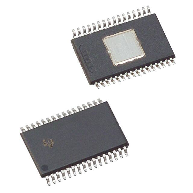
Available in 32 Pin HTSSOP DAP Package
(PD=3.9 W,
TA = 25°C)
LOD Function . . . LED Open Detection
(Error Signal Output at LED Disconnection)
TSD Function . . . Thermal Shutdown (Turn
Output Off When Junction Temperature
Exceeds Limit)
DAP PACKAGE
(TOP VIEW)
GND
BLANK
XLAT
SCLK
SIN
PGND
OUT0
OUT1
PGND
OUT2
OUT3
OUT4
OUT5
PGND
OUT6
OUT7
1
32
2
31
3
30
4
29
5
28
6
27
7
26
8
25
9
24
10
23
11
22
12
21
13
20
14
19
15
18
16
17
VCC
IREF
SOMODE
XDOWN
SOUT
PGND
OUT15
OUT14
PGND
OUT13
OUT12
OUT11
OUT10
PGND
OUT9
OUT8
description
The TLC5921 is a current-sink constant current driver incorporating shift register and data latch. The current
value at constant current output can be set by one external register. The device also incorporates thermal
shutdown (TSD) circuitry which turns constant current output off when the junction temperature exceeds the
limit, and LED open detection (LOD) circuitry to report the LED was disconnected.
Please be aware that an important notice concerning availability, standard warranty, and use in critical applications of
Texas Instruments semiconductor products and disclaimers thereto appears at the end of this data sheet.
Copyright 1999, Texas Instruments Incorporated
PRODUCTION DATA information is current as of publication date.
Products conform to specifications per the terms of Texas Instruments
standard warranty. Production processing does not necessarily include
testing of all parameters.
POST OFFICE BOX 655303
• DALLAS, TEXAS 75265
1
�TLC5921
LED DRIVER
SLLS390 – SEPTEMBER 1999
functional block diagram
VCC
SOMODE
SCLK
16 bits
Shift Register
SIN
Timing Selector
SOUT
16 bits
Data Latch
XLAT
100 kΩ
100 kΩ
BLANK
IREF
XDOWN
16 bits Constant Current Driver
and
LED Disconnection detection
TSD
GND
PGND
OUT0
2
OUT15
POST OFFICE BOX 655303
• DALLAS, TEXAS 75265
�TLC5921
LED DRIVER
SLLS390 – SEPTEMBER 1999
equivalent input and output schematic diagrams
Input (except SCLK)
Input (SCLK)
VCC
VCC
INPUT
INPUT
GND
GND
SOUT
VCC
OUTPUT
GND
XDOWN
XDOWN
GND
OUTn
OUTn
GND
POST OFFICE BOX 655303
• DALLAS, TEXAS 75265
3
�TLC5921
LED DRIVER
SLLS390 – SEPTEMBER 1999
Terminal Functions
ÁÁÁÁÁÁ
ÁÁÁÁÁÁ
ÁÁÁ
ÁÁÁÁÁÁÁÁÁÁÁÁÁÁÁÁÁÁÁÁÁÁ
ÁÁÁÁÁÁ
ÁÁÁÁÁÁ
ÁÁÁ
ÁÁÁÁÁÁÁÁÁÁÁÁÁÁÁÁÁÁÁÁÁÁ
ÁÁÁÁÁÁ
ÁÁÁÁÁÁ
ÁÁÁ
ÁÁÁÁÁÁÁÁÁÁÁÁÁÁÁÁÁÁÁÁÁÁ
ÁÁÁÁÁÁ
ÁÁÁÁÁÁ
ÁÁÁ
ÁÁÁÁÁÁÁÁÁÁÁÁÁÁÁÁÁÁÁÁÁÁ
ÁÁÁÁÁÁ
ÁÁÁÁÁÁ
ÁÁÁ
ÁÁÁÁÁÁÁÁÁÁÁÁÁÁÁÁÁÁÁÁÁÁ
ÁÁÁÁÁÁ
ÁÁÁÁÁÁ
ÁÁÁ
ÁÁÁÁÁÁÁÁÁÁÁÁÁÁÁÁÁÁÁÁÁÁ
ÁÁÁÁÁÁ
ÁÁÁÁÁÁ
ÁÁÁ
ÁÁÁÁÁÁÁÁÁÁÁÁÁÁÁÁÁÁÁÁÁÁ
ÁÁÁÁÁÁ
ÁÁÁÁÁÁ
ÁÁÁ
ÁÁÁÁÁÁÁÁÁÁÁÁÁÁÁÁÁÁÁÁÁÁ
ÁÁÁÁÁÁ
ÁÁÁÁÁÁ
ÁÁÁ
ÁÁÁÁÁÁÁÁÁÁÁÁÁÁÁÁÁÁÁÁÁÁ
ÁÁÁÁÁÁ
ÁÁÁÁÁÁ
ÁÁÁ
ÁÁÁÁÁÁÁÁÁÁÁÁÁÁÁÁÁÁÁÁÁÁ
ÁÁÁÁÁÁ
ÁÁÁÁÁÁ
ÁÁÁ
ÁÁÁÁÁÁÁÁÁÁÁÁÁÁÁÁÁÁÁÁÁÁ
ÁÁÁÁÁÁ
ÁÁÁÁÁÁ
ÁÁÁ
ÁÁÁÁÁÁÁÁÁÁÁÁÁÁÁÁÁÁÁÁÁÁ
ÁÁÁÁÁÁ
ÁÁÁÁÁÁ
ÁÁÁ
ÁÁÁÁÁÁÁÁÁÁÁÁÁÁÁÁÁÁÁÁÁÁ
ÁÁÁÁÁÁ
ÁÁÁÁÁÁ
ÁÁÁ
ÁÁÁÁÁÁÁÁÁÁÁÁÁÁÁÁÁÁÁÁÁÁ
ÁÁÁÁÁÁ
ÁÁÁÁÁÁ
ÁÁÁ
ÁÁÁÁÁÁÁÁÁÁÁÁÁÁÁÁÁÁÁÁÁÁ
ÁÁÁÁÁÁ
ÁÁÁÁÁÁ
ÁÁÁ
ÁÁÁÁÁÁÁÁÁÁÁÁÁÁÁÁÁÁÁÁÁÁ
ÁÁÁÁÁÁ
ÁÁÁÁÁÁ
ÁÁÁ
ÁÁÁÁÁÁÁÁÁÁÁÁÁÁÁÁÁÁÁÁÁÁ
ÁÁÁÁÁÁ
ÁÁÁÁÁÁ
ÁÁÁ
ÁÁÁÁÁÁÁÁÁÁÁÁÁÁÁÁÁÁÁÁÁÁ
ÁÁÁÁÁÁ
ÁÁÁÁÁÁ
ÁÁÁ
ÁÁÁÁÁÁÁÁÁÁÁÁÁÁÁÁÁÁÁÁÁÁ
ÁÁÁÁÁÁ
ÁÁÁÁÁÁ
ÁÁÁ
ÁÁÁÁÁÁÁÁÁÁÁÁÁÁÁÁÁÁÁÁÁÁ
ÁÁÁÁÁÁ
ÁÁÁÁÁÁ
ÁÁÁ
ÁÁÁÁÁÁÁÁÁÁÁÁÁÁÁÁÁÁÁÁÁÁ
ÁÁÁÁÁÁ
ÁÁÁÁÁÁ
ÁÁÁ
ÁÁÁÁÁÁÁÁÁÁÁÁÁÁÁÁÁÁÁÁÁÁ
TERMINAL
NAME
NO.
I/O
DESCRIPTION
SIN
5
I
1 bit serial data input
SOUT
28
O
1 bit serial data output
SCLK
4
I
Clock input for data transfer. All the data in the shift register is shifted to MSB by 1 bit
synchronizing to the rising edge of SCLK, and data at SIN is shifted to LSB at the same time.
(Schmitt buffer input)
XLAT
3
I
Latch. When XLAT is high, data on shift register goes through latch. When XLAT is low, data
is latched. Accordingly, if data on shift register is changed during XLAT high, this new value
is latched (level latch). This terminal is internally pulled down with 100kΩ.
SOMODE
30
I
Timing select for serial data output. When SOMODE is low, output data on SOUT is changed
synchronizing to the rising edge of SCLK. When SOMODE is high, output data on SOUT
is changed synchronizing to the falling edge of SCLK.
7,8,10,11,12,13,
15,16,17,18,20,
21,22,23,25,26
O
Constant current output.
BLANK
2
I
Blank(Light off). When BLANK is high, all the output of constant current driver is turned off.
When BLANK is low and data written to latch is 1, the corresponding constant current output
turns on (LED on). This terminal is internally pulled up with 100kΩ.
IREF
31
I
Constant current value setting. LED current is set to desired value by connecting external
resistor between IREF and GND. The 38 times current compared to current across external
resistor sink on output terminal.
XDOWN
29
O
Error output. XDOWN is configured as open collector. It goes low when TSD or LOD
functions.
VCC
32
Power supply voltage
GND
1
Ground
OUT0 – OUT15
PGND
6,9,14,19,24,27
Ground for LED driver. (Internally connected to GND)
THERMAL PAD
package bottom
Heat sink pad. This pad is connected to the lowest potential to IC or thermal layer.
absolute maximum ratings (see Note 1)†
Supply voltage, VCC . . . . . . . . . . . . . . . . . . . . . . . . . . . . . . . . . . . . . . . . . . . . . . . . . . . . . . . . . . . . . . . – 0.3 V to 7 V
Output current (dc), IO(LC) . . . . . . . . . . . . . . . . . . . . . . . . . . . . . . . . . . . . . . . . . . . . . . . . . . . . . . . . . . . . . . . . 90 mA
Input voltage range, VI . . . . . . . . . . . . . . . . . . . . . . . . . . . . . . . . . . . . . . . . . . . . . . . . . . . . . . – 0.3 V to VCC + 0.3 V
Output voltage range, VO(SOUT), VO(XDOWN) . . . . . . . . . . . . . . . . . . . . . . . . . . . . . . . . . – 0.3 V to VCC + 0.3 V
Output voltage range, VO(OUTn) . . . . . . . . . . . . . . . . . . . . . . . . . . . . . . . . . . . . . . . . . . . . . . . . . . . . – 0.3 V to 18 V
Storage temperature range, Tstg . . . . . . . . . . . . . . . . . . . . . . . . . . . . . . . . . . . . . . . . . . . . . . . . . . . – 40°C to 150°C
Continuous total power dissipation at (or below) TA = 25°C . . . . . . . . . . . . . . . . . . . . . . . . . . . . . . . . . . . . 3.9 W
Power dissipation rating at (or above) TA = 25°C . . . . . . . . . . . . . . . . . . . . . . . . . . . . . . . . . . . . . . . 31.4 mW/°C
† Stresses beyond those listed under “absolute maximum ratings” may cause permanent damage to the device. These are stress ratings only, and
functional operation of the device at these or any other conditions beyond those indicated under “recommended operating conditions” is not
implied. Exposure to absolute-maximum-rated conditions for extended periods may affect device reliability.
NOTE 1: All voltage values are with respect to GND terminal.
4
POST OFFICE BOX 655303
• DALLAS, TEXAS 75265
�TLC5921
LED DRIVER
SLLS390 – SEPTEMBER 1999
recommended operating conditions
ÁÁÁÁÁÁÁÁÁÁÁÁÁÁÁÁ
ÁÁÁÁÁÁÁÁÁ
ÁÁÁÁ
ÁÁÁ
ÁÁÁ
ÁÁÁ
ÁÁÁÁÁÁÁÁÁÁÁÁÁÁÁÁ
ÁÁÁÁÁÁÁÁÁ
ÁÁÁÁ
ÁÁÁ
ÁÁÁ
ÁÁÁ
ÁÁÁÁÁÁÁÁÁÁÁÁÁÁÁÁ
ÁÁÁÁÁÁÁÁÁ
ÁÁÁÁ
ÁÁÁ
ÁÁÁ
ÁÁÁ
ÁÁÁÁÁÁÁÁÁÁÁÁÁÁÁÁ
ÁÁÁÁÁÁÁÁÁ
ÁÁÁÁ
ÁÁÁ
ÁÁÁ
ÁÁÁ
ÁÁÁÁÁÁÁÁÁÁÁÁÁÁÁÁ
ÁÁÁÁÁÁÁÁÁ
ÁÁÁÁ
ÁÁÁ
ÁÁÁ
ÁÁÁ
ÁÁÁÁÁÁÁÁÁÁÁÁÁÁÁÁ
ÁÁÁÁÁÁÁÁÁ
ÁÁÁÁ
ÁÁÁ
ÁÁÁ
Á
ÁÁ
ÁÁÁ
ÁÁÁÁÁÁÁÁÁÁÁÁÁÁÁÁ
ÁÁÁÁÁÁÁÁÁ
ÁÁÁÁ
ÁÁÁ
ÁÁÁ
ÁÁÁ
ÁÁÁÁÁÁÁÁÁÁÁÁÁÁÁÁ
ÁÁÁÁÁÁÁÁÁ
ÁÁÁÁ
ÁÁÁ
ÁÁÁ
ÁÁÁ
ÁÁÁÁÁÁÁÁÁÁÁÁÁÁÁÁ
ÁÁÁÁÁÁÁÁÁ
ÁÁÁÁ
ÁÁÁ
ÁÁÁ
ÁÁÁ
ÁÁÁÁÁÁÁÁÁÁÁÁÁÁÁ
ÁÁÁÁÁÁÁÁÁÁÁ
ÁÁÁ
ÁÁÁ
ÁÁÁ
ÁÁÁ
ÁÁÁ
ÁÁÁÁÁÁÁÁÁÁÁÁÁ
ÁÁÁÁÁÁÁÁÁÁÁ
ÁÁÁ
ÁÁÁ
ÁÁÁ
ÁÁÁ
ÁÁÁÁÁÁÁÁÁÁÁÁÁÁÁ
ÁÁÁ
ÁÁÁÁÁÁÁÁÁÁÁÁÁ
ÁÁÁÁÁÁÁÁÁÁÁ
ÁÁÁ
ÁÁÁ
ÁÁÁ
ÁÁÁ
ÁÁÁ
ÁÁÁÁÁÁÁÁÁÁÁÁÁ
ÁÁÁÁÁÁÁÁÁÁÁ
ÁÁÁ
ÁÁÁ
ÁÁÁ
ÁÁÁ
ÁÁÁ
ÁÁÁÁÁÁÁÁÁÁÁÁÁ
ÁÁÁÁÁÁÁÁÁÁÁ
ÁÁÁ
ÁÁÁ
ÁÁÁ
ÁÁÁ
ÁÁÁ
ÁÁÁÁÁÁÁÁÁÁÁÁÁ
ÁÁÁÁÁÁÁÁÁÁÁ
ÁÁÁ
ÁÁÁ
ÁÁÁ
ÁÁÁ
ÁÁÁ
ÁÁÁÁÁÁÁÁÁÁÁÁÁ
ÁÁÁÁÁÁÁÁÁÁÁ
ÁÁÁ
ÁÁÁ
ÁÁÁÁ
ÁÁÁ
ÁÁ
Á
ÁÁÁ
ÁÁ
ÁÁÁ
ÁÁÁÁÁÁÁÁÁÁÁÁÁ
ÁÁÁÁÁÁÁÁÁÁÁ
ÁÁÁ
ÁÁÁ
ÁÁÁ
ÁÁÁ
ÁÁÁÁÁÁÁÁÁÁÁÁÁ
ÁÁÁÁÁÁÁÁÁÁÁ
ÁÁÁ
ÁÁÁ
ÁÁÁ
ÁÁÁ
ÁÁÁ
ÁÁÁÁÁÁÁÁÁÁÁÁÁ
ÁÁÁÁÁÁÁÁÁÁÁ
ÁÁÁ
ÁÁÁ
ÁÁÁ
ÁÁÁ
dc characteristics
PARAMETER
CONDITIONS
MIN
Supply voltage, VCC
NOM
4.5
Voltage applied to constant current output, VO
OUT0 to OUT15 off
High-level input voltage, VIH
Low-level output current, IOL
VCC = 4.5 V, SOUT
VCC = 4.5 V, SOUT, XDOWN
Constant output current, IO(LC)
OUT0 to OUT15
MAX
UNIT
5.5
V
17
V
0.8 VCC
VCC
V
GND
0.2 VCC
V
Low-level input voltage, VIL
High-level output current, IOH
5
Operating free-air temperature range, TA
–1
1
– 20
mA
80
mA
85
°C
ac characteristics, MIN/MAX: VCC = 4.5 V to 5.5 V, TA = –20 to 85°C
TYP: VCC = 5 V, TA = 25°C (unless otherwise noted)
PARAMETER
CONDITIONS
MIN
TYP
MAX
At single operation
20
At cascade operation (SOMODE = L)
15
fSCLK
SCLK clock frequency
twh/twl
twh
SCLK pulse duration
20
XLAT pulse duration
10
tr/tf
Rise/fall time
tsu
Setup time
th
Hold time
5
XLAT – SCLK
5
SIN – SCLK
20
XLAT – SCLK
20
POST OFFICE BOX 655303
• DALLAS, TEXAS 75265
MHz
ns
ns
100
SIN – SCLK
UNIT
ns
ns
ns
5
�TLC5921
LED DRIVER
SLLS390 – SEPTEMBER 1999
electrical characteristics, MIN/MAX: VCC = 4.5 V to 5.5 V, TA = – 20 to 85°C
TYP: VCC = 5 V, TA = 25°C (unless otherwise noted)
ÁÁÁÁÁÁÁÁÁÁÁÁÁÁÁ
ÁÁÁÁÁÁÁÁÁÁÁÁ
ÁÁÁ
ÁÁÁ
ÁÁÁ
ÁÁÁ
ÁÁÁÁÁ
ÁÁÁÁÁÁÁÁÁÁÁ
ÁÁÁÁÁÁÁÁÁÁÁÁ
ÁÁÁ
ÁÁÁ
ÁÁÁ
ÁÁÁ
ÁÁÁÁÁÁÁÁÁÁÁÁÁÁÁ
ÁÁÁÁÁ
ÁÁÁÁÁÁÁÁÁÁÁ
ÁÁÁÁÁÁÁÁÁÁÁÁ
ÁÁÁ
ÁÁÁ
ÁÁÁ
ÁÁÁ
ÁÁÁÁÁ
ÁÁÁÁÁÁÁÁÁÁÁ
ÁÁÁÁÁÁÁÁÁÁÁÁ
ÁÁÁ
ÁÁÁ
ÁÁÁ
ÁÁÁ
ÁÁÁ
ÁÁÁ
ÁÁÁÁÁ
ÁÁÁÁÁÁÁÁÁÁÁ
ÁÁÁÁÁÁÁÁÁÁÁÁ
ÁÁÁ
ÁÁÁ
ÁÁÁ
ÁÁÁ
ÁÁÁÁÁ
ÁÁÁÁÁÁÁÁÁÁÁ
ÁÁÁÁÁÁÁÁÁÁÁÁ
ÁÁÁ
ÁÁÁ
ÁÁÁ
ÁÁÁ
ÁÁÁÁÁ
ÁÁÁÁÁÁÁÁÁÁÁ
ÁÁÁÁÁÁÁÁÁÁÁÁ
ÁÁÁ
ÁÁÁ
ÁÁÁ
ÁÁÁ
ÁÁÁÁÁ
ÁÁÁÁÁÁÁÁÁÁÁ
ÁÁÁÁÁÁÁÁÁÁÁÁ
ÁÁÁ
ÁÁÁ
ÁÁÁ
ÁÁÁ
ÁÁÁÁÁ
ÁÁÁÁÁÁÁÁÁÁÁ
ÁÁÁÁÁÁÁÁÁÁÁÁ
ÁÁÁ
ÁÁÁ
ÁÁÁ
ÁÁÁ
ÁÁÁÁÁ
ÁÁÁÁÁÁÁÁÁÁÁ
ÁÁÁÁÁÁÁÁÁÁÁÁ
ÁÁÁ
ÁÁÁ
ÁÁÁ
ÁÁÁ
ÁÁÁÁÁ
ÁÁÁÁÁÁÁÁÁÁÁ
ÁÁÁÁÁÁÁÁÁÁÁÁ
ÁÁÁ
ÁÁÁ
ÁÁÁ
ÁÁÁ
ÁÁÁÁÁ
ÁÁÁÁÁÁÁÁÁÁÁ
ÁÁÁÁÁÁÁÁÁÁÁÁ
ÁÁÁ
ÁÁÁ
ÁÁÁ
ÁÁÁ
ÁÁÁÁÁ
ÁÁÁÁÁÁÁÁÁÁÁ
ÁÁÁÁÁÁÁÁÁÁÁÁ
ÁÁÁ
ÁÁÁ
ÁÁÁ
ÁÁÁ
ÁÁÁÁÁ
ÁÁÁÁÁÁÁÁÁÁÁ
ÁÁÁÁÁÁÁÁÁÁÁÁ
ÁÁÁ
ÁÁÁ
ÁÁÁ
ÁÁÁ
ÁÁÁÁÁ
ÁÁÁÁÁÁÁÁÁÁÁ
ÁÁÁÁÁÁÁÁÁÁÁÁ
ÁÁÁ
ÁÁÁ
ÁÁÁ
ÁÁÁ
ÁÁÁÁÁ
ÁÁÁÁÁÁÁÁÁÁÁ
ÁÁÁÁÁÁÁÁÁÁÁÁ
ÁÁÁ
ÁÁÁ
ÁÁÁ
ÁÁÁ
ÁÁÁÁÁ
ÁÁÁÁÁÁÁÁÁÁÁ
ÁÁÁÁÁÁÁÁÁÁÁÁ
ÁÁÁ
ÁÁÁ
ÁÁÁ
ÁÁÁ
ÁÁÁÁÁ
ÁÁÁÁÁÁÁÁÁÁÁ
ÁÁÁÁÁÁÁÁÁÁÁÁ
ÁÁÁ
ÁÁÁ
ÁÁÁ
ÁÁÁ
ÁÁÁÁÁ
ÁÁÁÁÁÁÁÁÁÁÁ
ÁÁÁÁÁÁÁÁÁÁÁÁ
ÁÁÁ
ÁÁÁ
ÁÁÁ
ÁÁÁ
ÁÁÁÁÁ
ÁÁÁÁÁÁÁÁÁÁÁ
ÁÁÁÁÁÁÁÁÁÁÁÁ
ÁÁÁ
ÁÁÁ
ÁÁÁ
ÁÁÁ
ÁÁÁÁÁ
ÁÁÁÁÁÁÁÁÁÁÁ
ÁÁÁÁÁÁÁÁÁÁÁÁ
ÁÁÁ
ÁÁÁ
ÁÁÁ
ÁÁÁ
ÁÁÁÁÁ
ÁÁÁÁÁÁÁÁÁÁÁ
ÁÁÁÁÁÁÁÁÁÁÁÁ
ÁÁÁ
ÁÁÁ
ÁÁÁ
ÁÁÁ
ÁÁÁÁÁ
ÁÁÁÁÁÁÁÁÁÁÁ
ÁÁÁÁÁÁÁÁÁÁÁÁ
ÁÁÁ
ÁÁÁ
ÁÁÁ
ÁÁÁ
ÁÁÁÁÁ
ÁÁÁÁÁÁÁÁÁÁÁ
ÁÁÁÁÁÁÁÁÁÁÁÁ
ÁÁÁ
ÁÁÁ
ÁÁÁ
ÁÁÁ
ÁÁÁÁÁÁÁÁÁÁÁÁÁÁÁ
ÁÁÁÁÁÁÁÁÁÁÁÁ
ÁÁÁ
ÁÁÁ
ÁÁÁ
ÁÁÁ
ÁÁÁ
ÁÁÁÁÁÁÁÁÁÁÁÁÁ
ÁÁÁÁÁÁÁÁÁÁÁÁ
ÁÁÁ
ÁÁÁ
ÁÁÁ
ÁÁÁ
ÁÁÁÁÁÁÁÁÁÁÁÁÁÁÁ
ÁÁÁ
ÁÁÁÁÁÁÁÁÁÁÁÁÁ
ÁÁÁÁÁÁÁÁÁÁÁÁ
ÁÁÁ
ÁÁÁ
ÁÁÁ
ÁÁÁ
ÁÁÁ
ÁÁÁÁÁÁÁÁÁÁÁÁÁ
ÁÁÁÁÁÁÁÁÁÁÁÁ
ÁÁÁ
ÁÁÁ
ÁÁÁ
ÁÁÁ
ÁÁÁ
ÁÁÁÁÁÁÁÁÁÁÁÁÁ
ÁÁÁÁÁÁÁÁÁÁÁÁ
ÁÁÁ
ÁÁÁ
ÁÁÁ
ÁÁÁ
ÁÁÁ
ÁÁÁ
ÁÁÁ
ÁÁÁÁÁÁÁÁÁÁÁÁÁ
ÁÁÁÁÁÁÁÁÁÁÁÁ
ÁÁÁ
ÁÁÁ
ÁÁÁ
ÁÁÁ
ÁÁÁ
ÁÁÁÁÁÁÁÁÁÁÁÁÁ
ÁÁÁÁÁÁÁÁÁÁÁÁ
ÁÁÁ
ÁÁÁ
ÁÁÁ
ÁÁÁ
ÁÁÁ
ÁÁÁÁÁÁÁÁÁÁÁÁÁ
ÁÁÁÁÁÁÁÁÁÁÁÁ
ÁÁÁ
ÁÁÁ
ÁÁÁ
ÁÁÁ
ÁÁÁ
ÁÁÁÁÁÁÁÁÁÁÁÁÁ
ÁÁÁÁÁÁÁÁÁÁÁÁ
ÁÁÁ
ÁÁÁ
ÁÁÁ
ÁÁÁ
ÁÁÁ
ÁÁÁÁÁÁÁÁÁÁÁÁÁ
ÁÁÁÁÁÁÁÁÁÁÁÁ
ÁÁÁ
ÁÁÁ
ÁÁÁ
ÁÁÁ
PARAMETER
TEST CONDITIONS
High-level output voltage
IOH = – 1 mA
VOL
II
Low-level output voltage
IOL = 1 mA
VI = VCC or GND (except BLANK, XLAT)
ICC
Supply current
TYP
MAX
VCC
–0.5V
VOH
Input current
MIN
UNIT
V
0.5
V
±1
µA
Input signal is static, VO = 1 V,
R(IREF) = 10 kΩ,
All output bits turn off
3
4.5
Input signal is static, VO = 1 V
RIREF = 1300 Ω,
All output bits turn off
7
9
Input signal is static, VO = 1 V,
R(IREF) = 640 Ω,
All output bits turn off
11
15
Data transfer,
R(IREF) = 1300 Ω,
VO = 1 V,
All output bits turn on
15
20
Data transfer,
R(IREF) = 640 Ω,
VO = 1 V,
All output bits turn on
35
50
VO = 1 V,
VO = 1 V
R(IREF) = 1300 Ω
R(IREF) = 640 Ω
35
40
45
mA
70
80
90
mA
0.1
µA
1
µA
mA
IOL(C1)
IOL(C2)
Constant output current
Ilkg
lk
Constant output leakage current
∆IO(LC)
Constant output current error between bit
VO = 1 V,
R(IREF) = 640 Ω,
All output bits turn on
±1
±4
%
I∆O(LC1)
Changes in constant output current
depend on supply voltage
Vref = 1.3 V
±1
±4
%/V
I∆O(LC2)
Changes in constant output current
depend on output voltage
VO = 1 V to 3 V,
Vref = 1.3 V,
±2
±6
%/V
T(tsd)
Vref
TSD detection temperature
Junction temperature
160
170
°C
Reference voltage
R(IREF) = 640 Ω
V(LEDDET)
LED disconnection detection voltage
Constant output current
OUT0 to OUT15 (V(OUTn) = 15 V)
XDOWN (5V pullup)
R(IREF) = 1300 Ω,
1 bit output turn on
150
1.3
V
0.3
V
switching characteristics, CL = 15 pF
PARAMETER
tr
Rise time
tf
Fall time
tpd
Propagation delay time
TEST CONDITIONS
TYP
15
OUTn (see Figure 1)
MAX
20
300
SOUT
5
OUTn
300
BLANK↑ – OUTn
400
650
BLANK↓ – OUTn
300
400
BLANK↑ – XDOWN (see Note 2)
600
1000
BLANK↓ – XDOWN (see Note 2)
500
1000
20
35
SCLK – SOUT
NOTE 2: At external resistor 5 kΩ
6
MIN
SOUT
POST OFFICE BOX 655303
• DALLAS, TEXAS 75265
10
15
UNIT
ns
ns
ns
�TLC5921
LED DRIVER
SLLS390 – SEPTEMBER 1999
PARAMETER MEASUREMENT INFORMATION
VCC
51 Ω
VCC
IREF
OUTn
GND
1300 Ω
15 pF
Figure 1. Rise Time and Fall Time Test Circuit for OUTn
100%
90%
VIH or VOH
100%
VIH or VOH
50%
10%
0%
VIL or VOL
tr
VIL or VOL
0%
tf
td1
100%
VIH
100%
50%
VIH or VOH
50%
0%
VIL
twh
0%
VIL or VOL
twl
Figure 2. Timing Requirements
POST OFFICE BOX 655303
• DALLAS, TEXAS 75265
7
�TLC5921
LED DRIVER
SLLS390 – SEPTEMBER 1999
PRINCIPLES OF OPERATION
setting for constant output current value
The constant current value is determined by external resistor, R(IREF) between IREF and GND. Refer constant
output current characteristics shown on Figure 5 for this external resistor value.
Note that more current flows if connect IREF to GND directly.
constant output current operation
When BLANK is low, the corresponding output is turned on if data latch value is 1, and turned off if data latch
value is 0. When BLANK is high, all outputs are forced to turn off. If there is constant current output terminal
left unconnected (includes LED disconnection), it should be lighted on after writing zero to corresponding data
latch to its output. If this operation is not done, supply current through constant current driver will increase.
shift register latch
The shift register latch is configured with 16 × 1 bits. The 1 bit for constant current output data represents ON
for constant current output if data is 1, or OFF if data is 0. The configuration of shift register latch is shown in
below.
Data Latch
XLATCH
OUT15
Data
OUT14
Data
OUT1
Data
OUT0
Data
(1 bits)
(1 bits)
(1 bits)
(1 bits)
15
2
1
Shift Register
SOUT
16
SCLK
SIN
Figure 3. Relationship Between Shift Register and Latch
SOUT output timing selection
By setting level of SOMODE, the SOUT output timing can be changed. When SOMODE is set to low, data is
clocked out to SOUT synchronized on the rising edge of SCLK, and when SOMODE is set to high, data is
clocked out to SOUT synchronized on the falling edge of SCLK. When SOMODE is set to high and shift
operation is done, the data shift error can be prevented even though SCLK signal is externally buffered in serial.
Note that the maximum data transfer rate in cascade operation is slower than that when SMODE is set to low.
TSD (thermal shutdown)
When the junction temperature exceeds the limit, TSD starts to function and turn constant current output off and
XDOWN goes low. Since XDOWN is configured with open-collector output, the outputs of multiple ICs can be
concatenated. To recover from constant current output off-state to normal operation, power supply should be
turned off and then turned on after several seconds.
8
POST OFFICE BOX 655303
• DALLAS, TEXAS 75265
�TLC5921
LED DRIVER
SLLS390 – SEPTEMBER 1999
PRINCIPLES OF OPERATION
LOD function (LED open detection)
If any terminal voltage of constant current output (OUT0 TO 15) to be turned on is approximately below 0.3 V,
XDOWN output goes low during output on by knowing LED disconnection. This function is operational for
sixteen OUTn individually. To know which constant current output is disconnected, the level of XDOWN is
repeatedly checked 16 times from OUT0 to OUT15 turning one constant current output on. The power supply
voltage for LED should be set to that the constant current output is applied to above 0.4 V to prevent from
XDOWN low when LED is lighting on normally. Note that on-time should be minimum1µs after the constant
current output is turned on since XDOWN output is required approximately 1 µs.
As discussed earlier, XDOWN is used for both TSD and LOD function. Therefore, BLANK is used to know which
one of TSD or LOD worked when XDOWN went low at LED disconnection, that is, in this condition, when set
BLANK to high, all the constant current outputs are turned off and LOD disconnection detection is disabled, then,
if XDOWN was changed to high, LED disconnection must be occurred.
Table 1 is an example for XDOWN output status using four LEDs.
ÁÁÁÁÁÁÁÁ
ÁÁÁÁÁ
ÁÁÁÁÁ
ÁÁÁÁÁ
ÁÁÁÁ
ÁÁÁÁÁÁÁÁ
ÁÁÁÁÁ
ÁÁÁÁÁ
ÁÁÁÁÁ
ÁÁÁÁ
ÁÁÁÁÁÁÁÁ
ÁÁÁÁÁ
ÁÁÁÁÁ
ÁÁÁÁÁ
ÁÁÁÁ
ÁÁÁÁÁÁÁÁ
ÁÁÁÁÁ
ÁÁÁÁÁ
ÁÁÁÁÁ
ÁÁÁÁ
ÁÁÁÁÁÁÁÁ
ÁÁÁÁÁÁÁÁÁÁÁÁÁÁÁÁ
ÁÁÁÁÁ
ÁÁÁÁÁ
ÁÁÁÁÁ
ÁÁÁÁ
ÁÁÁÁÁÁÁÁ
ÁÁÁÁÁ
ÁÁÁÁÁ
ÁÁÁÁÁ
ÁÁÁÁ
ÁÁÁÁÁÁÁÁÁÁÁÁÁÁÁÁ
ÁÁÁÁÁÁÁÁ
ÁÁÁÁÁ
ÁÁÁÁÁ
ÁÁÁÁÁ
ÁÁÁÁ
ÁÁÁÁÁÁÁÁ
ÁÁÁÁÁ
ÁÁÁÁÁ
ÁÁÁÁÁ
ÁÁÁÁ
ÁÁÁÁÁÁÁÁ
ÁÁÁÁÁÁÁÁÁÁÁÁÁÁÁÁ
ÁÁÁÁÁ
ÁÁÁÁÁ
ÁÁÁÁÁ
ÁÁÁÁ
ÁÁÁÁÁÁÁÁ
ÁÁÁÁÁ
ÁÁÁÁÁ
ÁÁÁÁÁ
ÁÁÁÁ
ÁÁÁÁÁÁÁÁÁÁÁÁÁÁÁÁ
ÁÁÁÁÁÁÁÁ
ÁÁÁÁÁ
ÁÁÁÁÁ
ÁÁÁÁÁ
ÁÁÁÁ
ÁÁÁÁÁÁÁÁ
ÁÁÁÁÁ
ÁÁÁÁÁ
ÁÁÁÁÁ
ÁÁÁÁ
ÁÁÁÁÁÁÁÁ
ÁÁÁÁÁ
ÁÁÁÁÁ
ÁÁÁÁÁ
ÁÁÁÁ
ÁÁÁÁÁÁÁÁ
ÁÁÁÁÁÁÁÁÁÁÁÁÁÁÁÁ
ÁÁÁÁÁ
ÁÁÁÁÁ
ÁÁÁÁÁ
ÁÁÁÁ
ÁÁÁÁÁÁÁÁ
ÁÁÁÁÁÁÁÁÁÁÁÁÁÁÁÁ
Table 1. XDOWN Output Example
LED NUMBER
1
2
3
4
LED STATUS
GOOD
NG
GOOD
NG
OUTn
ON
ON
ON
ON
DETECTION RESULT
GOOD
NG
GOOD
NG
XDOWN
LOW (by case 2, 4)
LED NUMBER
1
2
3
LED STATUS
GOOD
NG
GOOD
NG
OUTn
ON
ON
OFF
OFF
DETECTION RESULT
GOOD
NG
GOOD
GOOD
LED NUMBER
1
2
3
4
LED STATUS
GOOD
NG
GOOD
NG
XDOWN
4
LOW (by case 2)
OUTn
OFF
OFF
OFF
OFF
DETECTION RESULT
GOOD
GOOD
GOOD
GOOD
XDOWN2
HIGH–IMPEDANCE
noise reduction : output slope
When output current is 80 mA, the time to change constant current output to turn-on and turn-off is approximately
150 ns and 250 ns respectively. This allows to reduce concurrent switching noise occurred when multiple
outputs turn or off at the same time.
thermal pad
The thermal pad should be connected to GND to eliminate the noise influence since it is connected to the bottom
side of IC chip. Also, desired thermal effect will be obtained by connecting this pad to the PCB pattern with better
thermal conductivity.
POST OFFICE BOX 655303
• DALLAS, TEXAS 75265
9
�TLC5921
LED DRIVER
SLLS390 – SEPTEMBER 1999
PRINCIPLES OF OPERATION
3.9
3.2
2.0
1.48
0
Output Voltage (Constant Current) – V
PD – Total Power Dissipation – W
power rating – free-air temperature
0
–20
0
25
85
TA – Free–Air Temperature – °C
NOTES: A. The data is based on simulation result. When TI recommended print circuit board is used, derate linearly at the rate of 31.4 mW/°C
for operation above 25°C free-air temperature. VCC=5 V, IO(LC) = 80 mA, ICC is typical value.
B. The thermal impedance will be varied depend on mounting conditions. Since PZP package established low thermal impedance by
radiating heat from thermal pad, the thermal pad should be soldered to pattern with low thermal impedance.
C. The material for PCB should be selected considering the thermal characteristics since the temperature will rise around the thermal
pad.
Figure 4. Power Rating
10
POST OFFICE BOX 655303
• DALLAS, TEXAS 75265
�TLC5921
LED DRIVER
SLLS390 – SEPTEMBER 1999
PRINCIPLES OF OPERATION
constant output current
100000
R(ref) – Reference Resistance – ( Ω )
66000
13200
10000
6000
2750
1800
1300
1040
1000
860
730
640
100
0
10
20
30
40
50
60
70
80
Ilkg – Input Leakage Current – (mA)
Conditions : VO = 1 V, Vref = 1.3 V
NOTE: The resistor, R(IREF), should be located as close to IREF terminal as possible to avoid the noise influence.
Figure 5. Current on Constant Current Output vs External Resistor
POST OFFICE BOX 655303
• DALLAS, TEXAS 75265
11
�tsu (SIN–SCLK)
SD01_B
SD02_B
SD14_B
SD15_B
SD00_C
SD14_C
SD15_C
SD00_D
1/fSCLK
th (SIN–SCLK)
SCLK
twl (SCLK)
th (XLAT–SCLK)
twh (SCLK)
XLAT
POST OFFICE BOX 655303 • DALLAS, TEXAS 75265
tsu (XLAT–SCLK)
BLANK
SOMODE
SOUT
ÎÎÎÎ
ÎÎÎÎ
td (SCLK–SOUT)
SD00_A
OUTn
SD01_A
td (SCLK–SOUT)
SD02_A
SD14_A
SD15_A
SD00_B
td (SCLK–SOUT)
SD01_B
SD14_B
DRIVER ON
DRIVER OFF
td (BLANK–XDOWN)
td (BLANK–XDOWN)
XDOWN
HI–Z
NOTE : LED disconnected
Figure 6. Timing Diagram
SD00_C
td (BLANK–OUTn)
td (BLANK–OUTn)
DRIVER OFF
SD15_B
(Note)
Template Release Date: 7–11–94
SD00_B
TLC5921
LED DRIVER
SD15_A
SLLS390 – SEPTEMBER 1999
12
SIN
�PACKAGE OPTION ADDENDUM
www.ti.com
19-Oct-2022
PACKAGING INFORMATION
Orderable Device
Status
(1)
Package Type Package Pins Package
Drawing
Qty
Eco Plan
(2)
Lead finish/
Ball material
MSL Peak Temp
Op Temp (°C)
Device Marking
(3)
Samples
(4/5)
(6)
TLC5921DAP
ACTIVE
HTSSOP
DAP
32
46
RoHS & Green
NIPDAU
Level-3-260C-168 HR
-20 to 85
TLC5921
Samples
TLC5921DAPR
ACTIVE
HTSSOP
DAP
32
2000
RoHS & Green
NIPDAU
Level-3-260C-168 HR
-20 to 85
TLC5921
Samples
(1)
The marketing status values are defined as follows:
ACTIVE: Product device recommended for new designs.
LIFEBUY: TI has announced that the device will be discontinued, and a lifetime-buy period is in effect.
NRND: Not recommended for new designs. Device is in production to support existing customers, but TI does not recommend using this part in a new design.
PREVIEW: Device has been announced but is not in production. Samples may or may not be available.
OBSOLETE: TI has discontinued the production of the device.
(2)
RoHS: TI defines "RoHS" to mean semiconductor products that are compliant with the current EU RoHS requirements for all 10 RoHS substances, including the requirement that RoHS substance
do not exceed 0.1% by weight in homogeneous materials. Where designed to be soldered at high temperatures, "RoHS" products are suitable for use in specified lead-free processes. TI may
reference these types of products as "Pb-Free".
RoHS Exempt: TI defines "RoHS Exempt" to mean products that contain lead but are compliant with EU RoHS pursuant to a specific EU RoHS exemption.
Green: TI defines "Green" to mean the content of Chlorine (Cl) and Bromine (Br) based flame retardants meet JS709B low halogen requirements of