Sample &
Buy
Product
Folder
Support &
Community
Tools &
Software
Technical
Documents
TLC5947
SBVS114B – JULY 2008 – REVISED JANUARY 2015
TLC5947 24-Channel, 12-Bit PWM LED Driver With Internal Oscillator
1 Features
2 Applications
•
•
•
•
•
•
•
•
•
•
1
•
•
•
•
•
•
•
•
•
24 Channels, Constant-Current Sink Output
30-mA Capability (Constant-Current Sink)
12-Bit (4096 Steps) PWM Grayscale Control
LED Power-Supply Voltage Up to 30 V
VCC = 3.0 V to 5.5 V
Constant-Current Accuracy:
– Channel-to-Channel = ±2% (Typical)
– Device-to-Device = ±2% (Typical)
CMOS Logic Level I/O
30-MHz Data Transfer Rate (Standalone)
15-MHz Data Transfer Rate (Cascaded Devices,
SCLK Duty = 50%)
Shift Out Data Changes With Falling Edge to
Avoid Data Shift Errors
Auto Display Repeat
4-MHz Internal Oscillator
Thermal Shutdown (TSD):
– Automatic Shutdown at OverTemperature
Conditions
– Restart Under Normal Temperature
Noise Reduction:
– 4-Channel Grouped Delay to Prevent Inrush
Current
Operating Temperature: –40°C to 85°C
Static LED Displays
Message Boards
Amusement Illumination
TV Backlighting
3 Description
The TLC5947 is a 24-channel, constant-current sink
LED driver. Each channel is individually adjustable
with 4096 pulse-width modulated (PWM) steps. PWM
control is repeated automatically with the
programmed grayscale (GS) data. GS data are
written via a serial interface port. The current value of
all 24 channels is set by a single external resistor.
The TLC5947 has a thermal shutdown (TSD) function
that turns off all output drivers during an overtemperature condition. All of the output drivers
automatically restart when the temperature returns to
normal conditions.
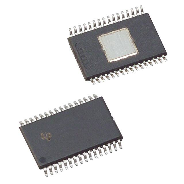
Device Information(1)
PART NUMBER
TLC5947
PACKAGE
BODY SIZE (NOM)
HTSSOP (32)
11.00 mm × 6.20 mm
VQFN (32)
5.00 mm × 5.00 mm
(1) For all available packages, see the orderable addendum at
the end of the datasheet.
Application Circuit
VLED
VLED
OUT0
DATA
¼
¼
¼
¼
¼
¼
¼
¼
¼
OUT23
XLAT
BLANK
BLANK
OUT0
SOUT
SCLK
XLAT
TLC5947
IC1
OUT23
SOUT
SCLK
XLAT
VCC
BLANK
GND
IREF
¼
SIN
VCC
RIREF
VLED
¼
SIN
SCLK
Controller
VLED
IREF
VCC
TLC5947
ICn
VCC
GND
RIREF
3
1
An IMPORTANT NOTICE at the end of this data sheet addresses availability, warranty, changes, use in safety-critical applications,
intellectual property matters and other important disclaimers. PRODUCTION DATA.
�TLC5947
SBVS114B – JULY 2008 – REVISED JANUARY 2015
www.ti.com
Table of Contents
1
2
3
4
5
6
7
Features ..................................................................
Applications ...........................................................
Description .............................................................
Revision History.....................................................
Pin Configuration and Functions .........................
Specifications.........................................................
1
1
1
2
3
4
6.1
6.2
6.3
6.4
6.5
6.6
6.7
6.8
4
4
5
5
5
6
7
9
Absolute Maximum Ratings .....................................
ESD Ratings..............................................................
Recommended Operating Conditions.......................
Thermal Information ..................................................
Dissipation Ratings ...................................................
Electrical Characteristics...........................................
Switching Characteristics ..........................................
Typical Characteristics ..............................................
Parameter Measurement Information ................ 11
7.1 Pin Equivalent Input and Output Schematic
Diagrams.................................................................. 11
7.2 Test Circuits ............................................................ 11
8
Detailed Description ............................................ 12
8.1
8.2
8.3
8.4
9
Overview .................................................................
Functional Block Diagram .......................................
Feature Description.................................................
Programming...........................................................
12
12
12
15
Application and Implementation ........................ 18
9.1 Application Information............................................ 18
9.2 Typical Application ................................................. 18
10 Power Supply Recommendations ..................... 20
11 Layout................................................................... 20
11.1 Layout Guidelines ................................................. 20
11.2 Layout Example .................................................... 20
11.3 Power Dissipation ................................................. 21
12 Device and Documentation Support ................. 22
12.1 Trademarks ........................................................... 22
12.2 Electrostatic Discharge Caution ............................ 22
12.3 Glossary ................................................................ 22
13 Mechanical, Packaging, and Orderable
Information ........................................................... 22
4 Revision History
Changes from Revision A (September 2008) to Revision B
•
2
Page
Added Pin Configuration and Functions section, ESD Ratings table, Feature Description section, Device Functional
Modes, Application and Implementation section, Power Supply Recommendations section, Layout section, Device
and Documentation Support section, and Mechanical, Packaging, and Orderable Information section .............................. 1
Submit Documentation Feedback
Copyright © 2008–2015, Texas Instruments Incorporated
Product Folder Links: TLC5947
�TLC5947
www.ti.com
SBVS114B – JULY 2008 – REVISED JANUARY 2015
5 Pin Configuration and Functions
32-PINS
DAP PACKAGE
(TOP VIEW)
OUT23
OUT1
6
27
OUT2
7
OUT3
8
OUT4
9
OUT5
OUT17
28
OUT16
5
17
SOUT
OUT0
OUT18
29
19
4
18
XLAT
SIN
OUT20
30
OUT19
3
21
IREF
SCLK
20
31
OUT22
2
OUT21
VCC
BLANK
22
32
OUT23
1
24
GND
23
32-PINS
RHB PACKAGE
(TOP VIEW)
SOUT
25
16
OUT15
OUT22
XLAT
26
15
OUT14
26
OUT21
IREF
27
14
OUT13
25
OUT20
VCC
28
13
OUT12
24
OUT19
10
23
OUT18
OUT6
11
22
OUT17
OUT7
12
21
OUT16
OUT8
13
20
OUT15
(1)
8
OUT7
OUT8
OUT6
9
6
32
7
SIN
OUT5
OUT9
4
10
5
OUT12
31
OUT3
17
SCLK
OUT4
16
OUT10
3
OUT13
OUT11
OUT11
11
OUT1
OUT14
18
12
30
OUT2
19
15
29
1
14
GND
BLANK
2
OUT9
OUT10
Thermal Pad
(Bottom Side)
OUT0
Thermal Pad
(Bottom Side)
This device is product preview.
Pin Functions
PIN
NAME
RHB NO. DAP NO.
I/O
DESCRIPTION
Blank (all constant-current outputs off). When BLANK is high, all constant-current outputs (OUT0
through OUT23) are forced off, the grayscale PWM timing controller initializes, and the grayscale
counter resets to '0'. When BLANK is low, all constant-current outputs are controlled by the
grayscale PWM timing controller.
BLANK
30
2
I
GND
29
1
—
Power ground
IREF
27
31
I/O
This pin sets the constant-current value. OUT0 through OUT23 constant sink current is set to the
desired value by connecting an external resistor between IREF and GND.
OUT0
1
5
O
Constant-current output. Multiple outputs can be tied together to increase the constant-current
capability. Different voltages can be applied to each output.
OUT1
2
6
O
Constant-current output
OUT2
3
7
O
Constant-current output
OUT3
4
8
O
Constant-current output
OUT4
5
9
O
Constant-current output
OUT5
6
10
O
Constant-current output
OUT6
7
11
O
Constant-current output
OUT7
8
12
O
Constant-current output
OUT8
9
13
O
Constant-current output
OUT9
10
14
O
Constant-current output
OUT10
11
15
O
Constant-current output
OUT11
12
16
O
Constant-current output
OUT12
13
17
O
Constant-current output
OUT13
14
18
O
Constant-current output
OUT14
15
19
O
Constant-current output
OUT15
16
20
O
Constant-current output
OUT16
17
21
O
Constant-current output
Submit Documentation Feedback
Copyright © 2008–2015, Texas Instruments Incorporated
Product Folder Links: TLC5947
3
�TLC5947
SBVS114B – JULY 2008 – REVISED JANUARY 2015
www.ti.com
Pin Functions (continued)
PIN
NAME
RHB NO. DAP NO.
I/O
DESCRIPTION
OUT17
18
22
O
Constant-current output
OUT18
19
23
O
Constant-current output
OUT19
20
24
O
Constant-current output
OUT20
21
25
O
Constant-current output
OUT21
22
26
O
Constant-current output
OUT22
23
27
O
Constant-current output
OUT23
24
28
O
Constant-current output
SCLK
31
3
I
Serial data shift clock. Schmitt buffer input. Data present on the SIN pin are shifted into the shift
register with the rising edge of the SCLK pin. Data are shifted to the MSB side by 1-bit
synchronizing of the rising edge of SCLK. The MSB data appears on SOUT at the falling edge of
SCLK. A rising edge on the SCLK input is allowed 100 ns after an XLAT rising edge.
SIN
32
4
I
Serial input for grayscale data
SOUT
25
29
O
Serial data output. This output is connected to the shift register placed after the MSB of the
grayscale shift register. Therefore, the MSB data of the grayscale shift register appears at the
falling edge of SCLK. This function reduces the data shifting errors caused by small timing
margins between SIN and SCLK.
VCC
28
32
—
Power-supply voltage
XLAT
26
30
I
The data in the grayscale shift register are moved to the grayscale data latch with a low-to-high
transition on this pin. When the XLAT rising edge is input, all constant-current outputs are forced
off until the next grayscale display period. The grayscale counter is not reset to zero with a rising
edge of XLAT.
6 Specifications
6.1 Absolute Maximum Ratings
Over operating free-air temperature range, unless otherwise noted. (1) (2)
VCC
Supply voltage: VCC
IO
Output current (dc)
OUT0 to OUT23
VI
Input voltage
SIN, SCLK, XLAT, BLANK
SOUT
OUT0 to OUT23
VO
Output voltage
TJ(MAX)
Operating junction temperature
Tstg
Storage temperature
(1)
(2)
MIN
MAX
–0.3
6.0
V
38
mA
–0.3
VCC + 0.3
V
–0.3
VCC + 0.3
V
–0.3
33
V
150
°C
150
°C
–55
UNIT
Stresses beyond those listed under Absolute Maximum Ratings may cause permanent damage to the device. These are stress ratings
only, which do not imply functional operation of the device at these or any other conditions beyond those indicated under Recommended
Operating Conditions. Exposure to absolute-maximum-rated conditions for extended periods may affect device reliability.
All voltage values are with respect to network ground terminal.
6.2 ESD Ratings
VALUE
V(ESD)
(1)
(2)
4
Electrostatic discharge
Human body model (HBM), per ANSI/ESDA/JEDEC JS-001, all
pins (1)
±2500
Charged device model (CDM), per JEDEC specification
JESD22-C101, all pins (2)
±500
UNIT
V
JEDEC document JEP155 states that 500-V HBM allows safe manufacturing with a standard ESD control process.
JEDEC document JEP157 states that 250-V CDM allows safe manufacturing with a standard ESD control process.
Submit Documentation Feedback
Copyright © 2008–2015, Texas Instruments Incorporated
Product Folder Links: TLC5947
�TLC5947
www.ti.com
SBVS114B – JULY 2008 – REVISED JANUARY 2015
6.3 Recommended Operating Conditions
At TA= –40°C to 85°C, unless otherwise noted.
MIN
NOM
MAX
UNIT
DC CHARACTERISTICS: VCC = 3 V to 5.5 V
VCC
Supply voltage
VO
Voltage applied to output OUT0 to OUT23
3.0
5.5
V
30
VIH
High-level input voltage
V
0.7 × VCC
VCC
V
VIL
Low-level input voltage
IOH
High-level output current SOUT
GND
0.3 × VCC
–3
mA
IOL
Low-level output current SOUT
3
mA
IOLC
Constant output sink current OUT0 to OUT23
2
30
mA
TA
Operating free-air temperature range
–40
85
°C
TJ
Operating junction temperature
–40
125
°C
SCLK, Standalone operation
30
MHz
SCLK, Duty 50%, cascade operation
15
MHz
V
AC CHARACTERISTICS: VCC = 3 V to 5.5 V
fSCLK
Data shift clock frequency
TWH0
TWL0
12
ns
SCLK = Low-level pulse width
10
ns
TWH1
XLAT, BLANK High-level pulse width
30
ns
TSU0
SIN–SCLK↑
5
ns
TSU1
Pulse duration
SCLK = High-level pulse width
XLAT↑–SCLK↑
100
ns
TSU2
Setup time
XLAT↑–BLANK↓
30
ns
TH0
SIN–SCLK↑
3
ns
XLAT↑–SCLK↑
10
ns
Hold time
TH1
6.4 Thermal Information
TLC5947
THERMAL METRIC
(1)
DAP
UNIT
32 PINS
RθJA
Junction-to-ambient thermal resistance
32.8
RθJC(top)
Junction-to-case (top) thermal resistance
17.1
RθJB
Junction-to-board thermal resistance
17.9
ψJT
Junction-to-top characterization parameter
0.4
ψJB
Junction-to-board characterization parameter
17.8
RθJC(bot)
Junction-to-case (bottom) thermal resistance
1.3
(1)
°C/W
For more information about traditional and new thermal metrics, see the IC Package Thermal Metrics application report, SPRA953.
6.5 Dissipation Ratings
(1)
(2)
(3)
PACKAGE
OPERATING FACTOR
ABOVE TA = 25°C
TA < 25°C
POWER RATING
TA = 70°C
POWER RATING
TA = 85°C
POWER RATING
HTSSOP-32 with
PowerPAD™ soldered (1)
42.54 mW/°C
5318 mW
3403 mW
2765 mW
HTSSOP-32 with
PowerPAD not soldered (2)
22.56 mW/°C
2820 mW
1805 mW
1466 mW
QFN-32 (3)
27.86 mW/°C
3482 mW
2228 mW
1811 mW
With PowerPAD soldered onto copper area on printed circuit board (PCB); 2 oz. copper. For more information, see SLMA002.
With PowerPAD not soldered onto copper area on PCB.
The package thermal impedance is calculated in accordance with JESD51-5.
Submit Documentation Feedback
Copyright © 2008–2015, Texas Instruments Incorporated
Product Folder Links: TLC5947
5
�TLC5947
SBVS114B – JULY 2008 – REVISED JANUARY 2015
www.ti.com
6.6 Electrical Characteristics
At VCC = 3.0 V to 5.5 V and TA = –40°C to 85°C. Typical values at VCC = 3.3 V and TA = 25°C, unless otherwise noted.
PARAMETER
TEST CONDITIONS
MIN
VOH
High-level output voltage
IOH = –3 mA at SOUT
VOL
Low-level output voltage
IOL = 3 mA at SOUT
IIN
Input current
VIN = VCC or GND at SIN, XLAT, and BLANK
TYP
VCC – 0.4
MAX
UNIT
VCC
V
–1
0.4
V
1
μA
ICC1
SIN/SCLK/XLAT = low, BLANK = high, VOUTn = 1 V,
RIREF = 24 kΩ
0.5
3
mA
ICC2
SIN/SCLK/XLAT = low, BLANK = high, VOUTn = 1 V,
RIREF = 3.3 kΩ
1
6
mA
ICC3
SIN/SCLK/XLAT = low, BLANK = low, VOUTn = 1 V,
RIREF = 3.3 kΩ, GSn = FFFh
15
45
mA
ICC4
SIN/SCLK/XLAT = low, BLANK = low, VOUTn = 1 V,
RIREF = 1.6 kΩ, GSn = FFFh
30
90
mA
30.75
33.8
mA
0.1
μA
Supply current (VCC)
IOLC
Constant output current
All OUTn = ON, VOUTn = 1 V, VOUTfix = 1 V,
RIREF = 1.6 kΩ
IOLK
Output leakage current
BLANK = high, VOUTn = 30 V, RIREF = 1.6 kΩ,
At OUT0 to OUT23
ΔIOLC
Constant-current error
(channel-to-channel) (1)
All OUTn = ON, VOUTn = 1 V, VOUTfix = 1 V,
RIREF = 1.6 kΩ, At OUT0 to OUT23
–4%
±2%
4%
ΔIOLC1
Constant-current error
(device-to-device) (2)
All OUTn = ON, VOUTn = 1 V, VOUTfix = 1 V,
RIREF = 1.6 kΩ
–7%
±2%
7%
ΔIOLC2
Line regulation (3)
All OUTn = ON, VOUTn = 1 V, VOUTfix = 1 V,
RIREF = 1.6 kΩ, At OUT0 to OUT23
±1
±3
%/V
ΔIOLC3
Load regulation (4)
All OUTn = ON, VOUTn = 1 V to 3 V, VOUTfix = 1 V,
RIREF = 1.6 kΩ, At OUT0 to OUT23
±2
±6
%/V
(5)
150
162
175
°C
5
10
20
°C
1.16
1.20
1.24
V
TDOWN
Thermal shutdown threshold
Junction temperature
THYS
Thermal error hysteresis
Junction temperature (5)
VIREF
Reference voltage output
RIREF = 1.6 kΩ
(1)
The deviation of each output from the average of OUT0–OUT23 constant-current. Deviation is calculated by the formula:
D (%) =
(2)
27.7
IOUTn
(IOUT0 + IOUT1 + ... + IOUT22 + IOUT23)
-1
´ 100
24
.
The deviation of the OUT0–OUT23 constant-current average from the ideal constant-current value. Deviation is calculated by the
following formula:
(IOUT0 + IOUT1 + ... IOUT22 + IOUT23)
24
D (%) =
- (Ideal Output Current)
´ 100
Ideal Output Current
Ideal current is calculated by the formula:
IOUT(IDEAL) = 41 ´
(3)
6
(IOUTn at VCC = 5.5 V) - (IOUTn at VCC = 3.0 V)
(IOUTn at VCC = 3.0 V)
´
100
5.5 V - 3 V
Load regulation is calculated by the equation:
D (%/V) =
(5)
RIREF
Line regulation is calculated by this equation:
D (%/V) =
(4)
1.20
(IOUTn at VOUTn = 3 V) - (IOUTn at VOUTn = 1 V)
(IOUTn at VOUTn = 1 V)
´
100
3V-1V
Not tested. Specified by design.
Submit Documentation Feedback
Copyright © 2008–2015, Texas Instruments Incorporated
Product Folder Links: TLC5947
�TLC5947
www.ti.com
SBVS114B – JULY 2008 – REVISED JANUARY 2015
6.7 Switching Characteristics
At VCC = 3.0 V to 5.5 V, TA = –40°C to 85°C, CL = 15 pF, RL = 150 Ω, RIREF = 1.6 kΩ, and VLED = 5.5 V. Typical values at VCC
= 3.3 V and TA = 25°C, unless otherwise noted.
PARAMETER
tR0
TEST CONDITIONS
Rise time
tR1
tF0
Fall time
tF1
TYP
MAX
SOUT
MIN
10
15
ns
OUTn
15
40
ns
SOUT
10
15
ns
OUTn
100
300
ns
4
5.6
MHz
Internal oscillator
frequency
fOSC
2.4
UNIT
tD0
SCLK↓ to SOUT
15
25
ns
tD1
BLANK↑ to OUT0 sink current off
20
40
ns
tD2
OUT0 current on to OUT1/5/9/13/17/21 current on
15
24
33
ns
tD3
Propagation delay time
OUT0 current on to OUT2/6/10/14/18/22 current on
30
48
66
ns
tD4
OUT0 current on to OUT3/7/11/15/19/23 current on
45
72
99
ns
TWH0, TWL0, TWH1:
VCC
(1)
INPUT
50%
GND
TWH
TWL
TSU0, TSU1, TSU2, TH0, TH1:
VCC
CLOCK
(1)
INPUT
50%
GND
TSU
TH
VCC
DATA/CONTROL
(1)
INPUT
50%
GND
(1)
Input pulse rise and fall time is 1 ns to 3 ns.
Figure 1. Input Timing
Submit Documentation Feedback
Copyright © 2008–2015, Texas Instruments Incorporated
Product Folder Links: TLC5947
7
�TLC5947
SBVS114B – JULY 2008 – REVISED JANUARY 2015
www.ti.com
tR0, tR1, tF0, tF1, tD0, tD1, tD2, tD3, tD4:
VCC
(1)
50%
INPUT
GND
tD
VOH or VOUTn
90%
50%
OUTPUT
10%
VOL or VOUTn
tR or tF
(1)
Input pulse rise and fall time is 1 ns to 3 ns.
Figure 2. Output Timing
SIN
GS0
0A
GS23 GS23
11B
10B
GS23
9B
TSU0
TH0
GS23 GS23
8B
7B
GS0
3B
fSCLK
GS0
2B
GS0
1B
GS0
0B
TH1
TWH0
GS23
11C
GS23
10C
GS23
9C
GS23
8C
GS23
7C
GS23
6C
GS23
5C
1
2
3
TWL0
4
5
6
7
TSU1
SCLK
1
2
3
4
285
5
286
287
288
TWH1
XLAT
TSU2
TWH1
BLANK
Grayscale
Latch Data
(Internal)
Oscillator
Clock
(Internal)
tD1
Previous Grayscale Data
Counter
4094 4096
Value ¼ 4093 4095 1 2 3 4
Latest Grayscale Data
fOSC
¼0 0 0 0 1 2 3 4 5 0 0 0 0 0 1 2
¼
¼
tD0
GS23
11A
SOUT
GS23
10A
GS23
9A
GS23 GS23
8A
7A
GS0
3A
GS0
2A
GS0
1A
GS0
0A
GS23
11B
GS23
10B
GS23
9B
GS23
8B
GS23
7B
GS23
6B
GS23
5B
tR0/tF0
OFF
OUT0/4/8/
12/16/20
(1)
OUT1/5/9/
13/17/21
(1)
OUT2/6/10/
14/18/22
(1)
OUT3/7/11/
15/19/23
(1)
(1)
ON
tR1
OFF
tF1
ON
tD2
OFF
ON
tD3
OFF
ON
tD4
GS data = FFFh.
Figure 3. Grayscale Data Write and OUTn Operation Timing
8
Submit Documentation Feedback
Copyright © 2008–2015, Texas Instruments Incorporated
Product Folder Links: TLC5947
�TLC5947
www.ti.com
SBVS114B – JULY 2008 – REVISED JANUARY 2015
6.8 Typical Characteristics
At VCC = 3.3 V and TA = 25°C, unless otherwise noted.
6000
Power Dissipation Rate (mW)
Reference Resistor (W)
100000
24600
9840
10000
4920
3280
2460
1968
TLC5947DAP
PowerPAD Soldered
5000
4000
TLC5947RHB
3000
TLC5947DAP
PowerPAD Not Soldered
2000
1000
1640
0
1000
0
15
10
5
20
30
25
-40
-20
Output Current (mA)
IO = 30 mA
Output Current (mA)
Output Current (mA)
33
IO = 25 mA
25
IO = 20 mA
20
IO = 15 mA
IO = 10 mA
10
IO = 2 mA
5
IO = 30 mA
34
30
15
IO = 5 mA
0
32
31
30
29
28
TA = -40°C
27
TA = +25°C
26
TA = +85°C
25
0
1.5
1.0
0.5
2.0
2.5
0
3.0
0.5
Figure 6. Output Current vs Output Voltage
1.5
2.0
2.5
3.0
Figure 7. Output Current vs Output Voltage
4
4
IO = 30 mA
TA = +25°C
3
3
2
2
1
1
DIOLC (%)
DIOLC (%)
1.0
Output Voltage (V)
Output Voltage (V)
0
-1
-2
0
-1
-2
VCC = 3.3 V
-3
-4
100
Figure 5. Power Dissipation Rate vs Free-Air Temperature
35
TA = +25°C
80
60
40
Free-Air Temperature (°C)
Figure 4. Reference Resistor vs Output Current
35
20
0
-40
-20
0
20
40
60
80
VCC = 3.3 V
-3
VCC = 5 V
100
-4
VCC = 5 V
0
5
10
15
20
25
Ambient Temperature (°C)
Output Current (mA)
Figure 8. ΔIOLC vs Ambient Temperature
Figure 9. ΔIOLC vs Output Current
Submit Documentation Feedback
Copyright © 2008–2015, Texas Instruments Incorporated
Product Folder Links: TLC5947
30
9
�TLC5947
SBVS114B – JULY 2008 – REVISED JANUARY 2015
www.ti.com
Typical Characteristics (continued)
At VCC = 3.3 V and TA = 25°C, unless otherwise noted.
Internal Oscillator Frequency (MHz)
5.0
4.5
4.0
CH1-OUT0
(GSData = 001h)
CH1 (2 V/div)
VCC = +3.3 V
VCC = +5 V
3.5
CH2 (2 V/div)
3.0
2.5
CH2-OUT0
(GSData = 002h)
2.0
1.5
IOLCMax = 30 mA
TA = +25°C
RL = 150 W
CL = 15 pF
VLED = 5.5 V
CH3 (2 V/div)
1.0
CH3-OUT23
(GSData = 003h)
0.5
0
-40
-20
0
20
35
55
70
Time (100 ns/div)
85
Ambient Temperature (°C)
Figure 10. Internal Oscillator Frequency vs Ambient
Temperature
10
Figure 11. Constant-Current Output Voltage Waveform
Submit Documentation Feedback
Copyright © 2008–2015, Texas Instruments Incorporated
Product Folder Links: TLC5947
�TLC5947
www.ti.com
SBVS114B – JULY 2008 – REVISED JANUARY 2015
7 Parameter Measurement Information
7.1 Pin Equivalent Input and Output Schematic Diagrams
VCC
VCC
INPUT
SOUT
GND
GND
Figure 12. SIN, SCLK, XLAT, BLANK
Figure 13. SOUT
OUTn
GND
Figure 14. OUT0 Through OUT23
7.2 Test Circuits
RL
VCC
VCC
VCC
OUTn
IREF
RIREF
VLED
SOUT
VCC
CL
GND
GND
Figure 15. Rise Time and Fall Time Test Circuit for
OUTn
VCC
Figure 16. Rise Time and Fall Time Test Circuit for
SOUT
OUT0
¼
VCC
CL
IREF
OUTn
¼
RIREF
GND OUT23
VOUTn
VOUTFIX
Figure 17. Constant-Current Test Circuit for OUTn
Submit Documentation Feedback
Copyright © 2008–2015, Texas Instruments Incorporated
Product Folder Links: TLC5947
11
�TLC5947
SBVS114B – JULY 2008 – REVISED JANUARY 2015
www.ti.com
8 Detailed Description
8.1 Overview
The TLC5947 is a 24-channel, constant-current sink driver. Each channel has an individually-adjustable, 4096step, PWM grayscale (GS) brightness control. The GS data is input through a serial interface port.
The TLC5947 has a 30-mA current capability. The maximum current value of all channels is determined by an
external resistor.
The TLC5947 can work without external CLK signals because the device is integrated with a 4-MHz internal
oscillator.
The device has a thermal shutdown (TSD) function that turns off all output drivers at over temperature conditions.
All of the output drivers automatically restart when the temperature returns to normal conditions.
8.2 Functional Block Diagram
VCC
VCC
LSB
MSB
SIN
D Q
Grayscale (12 Bits ´ 24 Channels) Data
Shift Register
SCLK
0
SOUT
CK
287
288
MSB
LSB
Grayscale (12 Bits ´ 24 Channels) Data
Data Latch
XLAT
287
0
288
4 MHz
Internal
Oscillator
12 Bits PWM Timing Control
Thermal
Detection
24
BL ANK
IREF
24-Channel, Constant Current Driver
GND
¼
OUT0
OUT1
OUT22
OUT23
8.3 Feature Description
8.3.1 Grayscale (GS) Control Function
Each constant-current sink output OUT0–OUT23 (OUTn) turns on (starts to sink constant current) at the fifth
rising edge of the grayscale internal oscillator clock after the BLANK signal transitions from high to low if the
grayscale data latched into the grayscale data latch are not zero. After turn-on, the number of rising edges of the
internal oscillator is counted by the 12-bit grayscale counter. Each OUTn output is turned off once its
corresponding grayscale data values equal the grayscale counter or the counter reaches 4096d (FFFh). The
PWM control operation is repeated as long as BLANK is low. OUTn is not turned on when BLANK is high. The
timing is shown in Figure 18. All outputs are turned off at the XLAT rising edge. After that, each output is
controlled again from the first clock of the internal oscillator for the next display period, based on the latest
grayscale data.
12
Submit Documentation Feedback
Copyright © 2008–2015, Texas Instruments Incorporated
Product Folder Links: TLC5947
�TLC5947
www.ti.com
SBVS114B – JULY 2008 – REVISED JANUARY 2015
Feature Description (continued)
When the IC is powered on, the data in the grayscale data shift register and latch are not set to default values.
Therefore, grayscale data must be written to the GS latch before turning on the constant-current output. BLANK
should be at a high level when powered on to keep the outputs off until valid grayscale data are written to the
latch. This avoids the LED being randomly illuminated immediately after power-up. If having the outputs turn on
at power-up is not a problem for the application, then BLANK does not need to be held high. The grayscale
functions can be controlled directly by grayscale data writing, even though BLANK is connected to GND.
BLANK
64
Counter Value
Internal
Oscillator
Clock
0 0 0 0 1 2 3
63
66
65
1027
1030
1026
1029
1025
1028
1031
2049
2052
2048
2051
2047
2050
3076
3073
3072
3075
3071
3074
3077
4096
4095
4094
1 2
Grayscale counter starts to count from 5th clock of the internal oscillator clock after BLANK goes low.
OUTn
(GS Data = 000h)
OFF
OUTn
(GS Data = 001h)
OFF
OUTn
(GS Data = 002h)
OFF
OUTn
(GS Data = 003h)
OFF
ON
Drivers do not turn on when grayscale data are ‘0’.
Dotted line indicates BLANK is high.
T = Internal CLK ´ 1
ON
T = Internal CLK ´ 2
ON
T = Internal CLK ´ 3
ON
OFF
OUTn
(GS Data = 040h)
OFF
OUTn
(GS Data = 041h)
OFF
¼
¼
OUTn
(GS Data = 03Fh)
T = Internal
CLK ´ 63
ON
T = Internal CLK ´ 64
ON
T = Internal CLK ´ 65
ON
¼
¼
OUTn
(GS Data = 400h)
OFF
OUTn
(GS Data = 401h)
OFF
T = Internal CLK ´ 1024
ON
T = Internal CLK ´ 1025
¼
¼
ON
OUTn
(GS Data = 800h)
OFF
ON
¼
¼
OUTn
(GS Data = C00h)
T = Internal CLK ´ 2048
OFF
T = Internal CLK ´ 3072
ON
¼
¼
OUTn
(GS Data = FFEh)
OFF
OUTn
(GS Data = FFFh)
OFF
T = Internal CLK ´ 4094
ON
T = Internal CLK ´ 4095
ON
Figure 18. PWM Operation
Submit Documentation Feedback
Copyright © 2008–2015, Texas Instruments Incorporated
Product Folder Links: TLC5947
13
�TLC5947
SBVS114B – JULY 2008 – REVISED JANUARY 2015
www.ti.com
Feature Description (continued)
8.3.2 Auto Display Repeat Function
This function can repeat the total display period without any timing control signal, as shown in Figure 19.
BLANK
GS Counter Value
¼
0 0 0 0 1 2 3
2048 ¼ 4095
¼ 2048 ¼ 4095
2047 2049 4094 0 1 2 3 2047 2049 4094 0
¼
1 2 3 0 0 0 0 0 0
1 2
4095
4094 4096 1 2
Internal Oscillator Clock
Grayscale counter starts to count from the fifth clock
of the internal oscillator clock after BLANK goes low.
Display period is turned on again by
the auto display repeat function.
OUTn OFF
(GS Data = 001h) ON
OUTn OFF
(GS Data = 800h) ON
OUTn OFF
(GS Data = FFFh) ON
First Display Period
(4096 Internal Clock)
First
Display Period
Second Display Period
(4096 Internal Clock)
Four Internal Clock Intervals After BLANK Goes Low
Nth Display Period
Second
Display Period
Four Internal Clock Intervals After BLANK Goes Low
Figure 19. Auto Display Repeat Operation
8.3.3 Thermal Shutdown (TSD)
The thermal shutdown (TSD) function turns off all constant-current outputs immediately when the IC junction
temperature exceeds the high temperature threshold (T(TEF) = +162° C, typ). The outputs will remain disabled as
long as the over-temperature condition exists. The outputs are turned on again at the first clock after the IC
junction temperature falls below the temperature of T(TEF) – T(HYS). Figure 20 shows the TSD operation.
TJ < T(TEF) - T(HYS)
IC Junction Temperature (TJ)
TJ < T(TEF) - T(HYS)
TJ ³ T(TEF)
TJ ³ T(TEF)
High
BLANK
Low
4096
1 2 3
4095
4096
4096
1 2
4095
1 2
4095
4096
1 2
4095
4096
1 2
4095
4096
1 2
4095
1 2
Internal Oscillator Clock
OFF
OUTn
(GS Data = FFFh)
OFF
ON
OFF
ON
Figure 20. TSD Operation
8.3.4 Noise Reduction
Large surge currents may flow through the IC and the board on which the device is mounted if all 24 LED
channels turn on simultaneously at the start of each grayscale cycle. These large current surges could introduce
detrimental noise and electromagnetic interference (EMI) into other circuits. The TLC5947 turns on the LED
channels in a series delay, to provide a current soft-start feature. The output current sinks are grouped into four
groups of six channels each. The first group is OUT0, 4, 8, 12, 16, 20; the second group is OUT1, 5, 9, 13, 17,
21; the third group is OUT2, 6, 10, 14, 18, 22; and the fourth group is OUT3, 7, 11, 15, 19, 23. Each group turns
on sequentially with a small delay between groups; see Figure 3. Both turn-on and turn-off are delayed.
14
Submit Documentation Feedback
Copyright © 2008–2015, Texas Instruments Incorporated
Product Folder Links: TLC5947
�TLC5947
www.ti.com
SBVS114B – JULY 2008 – REVISED JANUARY 2015
8.4 Programming
8.4.1 Register Configuration
The TLC5947 has a grayscale (GS) data shift register and data latch. Both the GS data shift register and latch
are 288 bits long and are used to set the PWM timing for the constant-current driver. Table 1 shows the on duty
cycle for each GS data. Figure 21 shows the shift register and data latch configuration. The data at the SIN pin
are shifted to the LSB of the shift register at the rising edge of the SCLK pin; SOUT data are shifted out on the
falling edge of SCLK. The timing diagram for data writing is shown in Figure 22. The driver on duty is controlled
by the data in the GS data latch.
Grayscale Data Shift Register (12 Bits ´ 24 Channels)
GS Data for OUT23
MSB
287
SOUT
GS Data for
Bit 11 of
OUT23
¼
GS Data for OUT22
276
275
GS Data for
Bit 0 of
OUT23
GS Data for
Bit 11 of
OUT22
¼
¼
GS Data for
Bit 11 of
OUT23
¼
GS Data for OUT0
LSB
0
12
11
GS Data for
Bit 0 of OUT1
GS Data for
Bit 11 of
OUT0
GS Data for OUT22
276
275
GS Data for
Bit 0 of
OUT23
GS Data for
Bit 11 of
OUT22
Grayscale Data Latch (12 Bits ´ 24 Channels)
¼ GS Data for OUT1
¼
¼
GS Data for
Bit 0 of OUT0
SIN
SCLK
¼
¼
GS Data for OUT23
MSB
287
¼ GS Data for OUT1
GS Data for OUT0
12
11
GS Data for
Bit 0 of OUT1
GS Data for
Bit 11 of
OUT0
LSB
0
¼
GS Data for
Bit 0 of OUT0
XLAT
288 Bits
To PWM Timing Control Block
Figure 21. Grayscale Data Shift Register and Latch Configuration
Submit Documentation Feedback
Copyright © 2008–2015, Texas Instruments Incorporated
Product Folder Links: TLC5947
15
�TLC5947
SBVS114B – JULY 2008 – REVISED JANUARY 2015
www.ti.com
Programming (continued)
Table 1. GS Data versus On Duty
GS DATA
(Binary)
GS DATA
(Decimal)
GS DATA
(Hex)
DUTY OF DRIVER TURN-ON
TIME (%)
0000 0000 0000
0
000
0.00
0000 0000 0001
1
001
0.02
0000 0000 0010
2
002
0.05
0000 0000 0011
3
003
0.07
—
—
—
—
0111 1111 1111
2047
7FF
49.98
1000 0000 0000
2048
800
50.00
1000 0000 0001
2049
801
50.02
—
—
—
—
1111 1111 1101
4093
FFD
99.93
1111 1111 1110
4094
FFE
99.95
1111 1111 1111
4095
FFF
99.98
GS data are transferred from the shift register to the latch by the rising edge of XLAT. When powered up, the
data in the grayscale shift register and data latch are not set to default values. Therefore, grayscale data must be
written to the GS latch before turning on the constant-current output. BLANK should be at a high level when
powered on to avoid falsely turning on the constant-current outputs due to random values in the latch at powerup. All of the constant-current outputs are forced off when BLANK is high. However, if the random values turning
on at power-up is not a concern in the application, BLANK can be at any level. GS can be controlled correctly
with the grayscale data writing functions, even if BLANK is connected to GND. Equation 1 determines each
output on duty.
GSn
´ 100
On Duty (%) =
4096
where
•
16
GSn = the programmed grayscale value for OUTn (GSn = 0 to 4095)
Submit Documentation Feedback
(1)
Copyright © 2008–2015, Texas Instruments Incorporated
Product Folder Links: TLC5947
�TLC5947
www.ti.com
SBVS114B – JULY 2008 – REVISED JANUARY 2015
SIN
GS0
0A
GS23 GS23
11B
10B
GS23
9B
GS23 GS23
8B
7B
GS0
2B
GS0
3B
GS0
1B
GS0
0B
GS23
11C
GS23
10C
1
2
GS23 GS23 GS23 GS23
9C
8C
7C
6C
SCLK
1
2
3
4
5
285
286
287
288
3
4
5
6
7
XLAT
GS0
0A
GS23 GS23
11B
10B
GS23
9B
GS23
8B
GS0
3B
GS0
2B
GS0
1B
GS0
0B
GS23
11C
GS23
10C
GS23
9C
GS23
8C
GS23
7C
GS23
6C
Shift Register
Bit 1 Data (Internal)
GS0
1A
GS0 GS23
0A
11B
GS23
10B
GS23
9B
GS0
4B
GS0
3B
GS0
2B
GS0
1B
GS0
0B
GS23
11C
GS23 GS23
10C
9C
GS23
8C
GS23
7C
Shift Register
Bit 286 Data (Internal)
GS23
10A
GS23 GS23
9A
8A
GS23
7A
GS23
6A
GS0
1A
GS0
0A
GS23
11B
GS23
10B
GS23
9B
GS23
8B
GS23
7B
GS23
6B
GS23
5B
GS23
4B
Shift Register
Bit 287 Data (Internal)
GS23
11A
GS23 GS23
10A
9A
GS23
8A
GS23
7A
GS0
2A
GS0
1A
GS23
0A
GS23
11B
GS23
10B
GS23
9B
GS23
8B
GS23 GS23
7B
6B
GS23
5B
¼
¼
¼
¼
Shift Register
Bit 0 Data (Internal)
Grayscale Latch Data
(Internal)
Latest Grayscale Latch Data
Previous Grayscale Latch Data
GS23
11A
SOUT
GS23
10A
GS23
9A
GS0
3A
GS23 GS23
8A
7A
GS0
2A
GS0
1A
GS0
0A
GS23
11B
4094 4096
¼ 4093
4095
GS23
10B
GS23
9B
GS23 GS23
8B
7B
GS23
6B
GS23
5B
4094 4096
1 2 3 4
¼ 4093
¼
4095
1 2 3 4 5 6 7 8
¼
Oscillator Clock
(Internal)
OFF
OFF
(1)
ON
(1)
ON
(1)
ON
(1)
ON
OUT0/4/8/12/16/20
ON
OFF
OUT1/5/9/13/17/21
OFF
ON
ON
ON
OFF
OFF
OUT3/7/11/15/19/23
ON
OFF
OFF
OUT2/6/10/14/18/22
ON
ON
ON
ON
(1) GS data = FFFh.
Figure 22. Grayscale Data Write Operation
Submit Documentation Feedback
Copyright © 2008–2015, Texas Instruments Incorporated
Product Folder Links: TLC5947
17
�TLC5947
SBVS114B – JULY 2008 – REVISED JANUARY 2015
www.ti.com
9 Application and Implementation
NOTE
Information in the following applications sections is not part of the TI component
specification, and TI does not warrant its accuracy or completeness. TI’s customers are
responsible for determining suitability of components for their purposes. Customers should
validate and test their design implementation to confirm system functionality.
9.1 Application Information
The device is a 24-channel, constant sink current, LED driver. This device can be connected in series to drive
many LED lamps with only a few controller ports. Output current control data and PWM control data can be
written from the SIN input terminal. The PWM timing reference clock can be supplied from the internal oscillation.
9.2 Typical Application
VLED
VLED
OUT0
DATA
Controller
¼
¼
¼
¼
¼
¼
¼
¼
¼
OUT23
BLANK
TLC5947
IC1
OUT23
SOUT
SCLK
XLAT
VCC
BLANK
GND
IREF
¼
SIN
VCC
XLAT
BLANK
OUT0
SOUT
SCLK
XLAT
VLED
¼
SIN
SCLK
VLED
VCC
TLC5947
ICn
IREF
RIREF
VCC
GND
RIREF
3
Figure 23. Typical Application Circuit (Multiple Daisy Chained TLC5947s)
9.2.1 Design Requirements
For this design example, use Table 2 as the input parameters.
Table 2. Design Parameters
DESIGN PARAMETER
EXAMPLE VALUE
VCC input voltage range
3 V to 5.5 V
LED lamp (VLED) input voltage range
Maximum LED forward voltage (VF) + IC knee voltage
SIN, SCLK, LAT, and BLANK voltage range
Low level = GND, High level = VCC
9.2.2 Detailed Design Procedure
9.2.2.1 Define Basic Parameters
To
•
•
•
18
begin the design process, a few parameters must be decided as following:
Maximum output constant-current value for each color LED lamp
Maximum LED forward voltage (VF)
Are auto display function used
Submit Documentation Feedback
Copyright © 2008–2015, Texas Instruments Incorporated
Product Folder Links: TLC5947
�TLC5947
www.ti.com
SBVS114B – JULY 2008 – REVISED JANUARY 2015
9.2.2.2 Grayscale (GS) Data
There are a total of 24 sets of 12-bit GS data for the PWM control of each output. Select the GS data of each
LED lamp and write the GS data to the register following the signal timing.
9.2.2.3 Auto-Display Function
There are a total of 24 sets of 12-bit GS data for the PWM control of each output. Select the GS data of each
LED lamp and write the GS data to the register following the signal timing.
9.2.2.4 Setting for the Constant Sink Current Value
The constant-current value for all channels is set by an external resistor (RIREF) placed between IREF and GND.
The resistor (RIREF) value is calculated by Equation 2.
RIREF (W) = 41 ´
VIREF (V)
IOLC (mA)
where
•
VIREF = the internal reference voltage on the IREF pin (typically 1.20 V).
(2)
IOLC must be set in the range of 2 mA to 30 mA. The constant sink current characteristic for the external resistor
value is shown in Figure 4. Table 3 describes the constant-current output versus external resistor value.
Table 3. Constant-Current Output versus External Resistor Value
IOLC (mA, Typical)
RIREF (Ω)
30
1640
25
1968
20
2460
15
3280
10
4920
5
9840
2
24600
9.2.3 Application Curves
Figure 24. Output Waveform with GS Data Latch Input
Figure 25. Output Waveform without GS Data Latch Input
Submit Documentation Feedback
Copyright © 2008–2015, Texas Instruments Incorporated
Product Folder Links: TLC5947
19
�TLC5947
SBVS114B – JULY 2008 – REVISED JANUARY 2015
www.ti.com
10 Power Supply Recommendations
The VCC power supply voltage should be decoupled by placing a 0.1-µF ceramic capacitor close to the VCC pin
and GND plane. Depending on the panel size, several electrolytic capacitors must be placed on the board
equally distributed to get a well regulated LED supply voltage (VLED). The VLED voltage ripple must be less than
5% of its nominal value. Furthermore, the VLED must be set to the voltage calculated by Equation 3:
VLED > VF + 0.4 V (10-mA constant-current example)
where
•
VF = maximum forward voltage of all LEDs.
(3)
11 Layout
11.1 Layout Guidelines
•
•
•
•
•
Place the decoupling capacitor near the VCC pin and GND plane.
Place the current programming resistor RIREF close to the IREF pin and the IREFGND pin.
Route the GND pattern as widely as possible for large GND currents.
The routing wire between the LED cathode side and the device OUTXn pin must be as short and straight as
possible to reduce wire inductance.
When several ICs are chained, symmetric placements are recommended.
11.2 Layout Example
BLANK
SCLK
SIN
OUT0
OUT1
OUT2
XLAT
BLANK
SCLK
SIN
GND
GND
VCC
GND
1
2
32
31
VCC
IREF
3
30
4
5
29
28
XLAT
SOUT
6
7
Thermal
Pad
27
26
OUT3
OUT4
OUT5
8
OUT6
OUT7
OUT8
11
12
13
20
OUT9
OUT10
OUT11
14
15
19
18
16
17
9
10
25
Via to
Heatsink
Layer
24
23
22
21
OUT23
OUT22
OUT21
OUT20
OUT19
OUT18
OUT17
OUT16
OUT15
OUT14
OUT13
OUT12
Figure 26. Layout Schematic
20
Submit Documentation Feedback
Copyright © 2008–2015, Texas Instruments Incorporated
Product Folder Links: TLC5947
�TLC5947
www.ti.com
SBVS114B – JULY 2008 – REVISED JANUARY 2015
11.3 Power Dissipation
The device power dissipation must be below the power dissipation rate of the device package (illustrated in
Figure 5) to ensure correct operation. Equation 4 calculates the power dissipation of the device:
PD = (VCC ´ ICC) + (VOUT ´ IOLC ´ N ´ dPWM)
where
•
•
•
•
•
•
VCC = device supply voltage
ICC = device supply current
VOUT = OUTn voltage when driving LED current
IOLC = LED current adjusted by RIREF resistor
N = number of OUTn driving LED at the same time
dPWM = duty ratio defined by GS value
(4)
Submit Documentation Feedback
Copyright © 2008–2015, Texas Instruments Incorporated
Product Folder Links: TLC5947
21
�TLC5947
SBVS114B – JULY 2008 – REVISED JANUARY 2015
www.ti.com
12 Device and Documentation Support
12.1 Trademarks
PowerPAD is a trademark of Texas Instruments.
All other trademarks are the property of their respective owners.
12.2 Electrostatic Discharge Caution
These devices have limited built-in ESD protection. The leads should be shorted together or the device placed in conductive foam
during storage or handling to prevent electrostatic damage to the MOS gates.
12.3 Glossary
SLYZ022 — TI Glossary.
This glossary lists and explains terms, acronyms, and definitions.
13 Mechanical, Packaging, and Orderable Information
The following pages include mechanical, packaging, and orderable information. This information is the most
current data available for the designated devices. This data is subject to change without notice and revision of
this document. For browser-based versions of this data sheet, refer to the left-hand navigation.
22
Submit Documentation Feedback
Copyright © 2008–2015, Texas Instruments Incorporated
Product Folder Links: TLC5947
�PACKAGE OPTION ADDENDUM
www.ti.com
19-Oct-2022
PACKAGING INFORMATION
Orderable Device
Status
(1)
Package Type Package Pins Package
Drawing
Qty
Eco Plan
(2)
Lead finish/
Ball material
MSL Peak Temp
Op Temp (°C)
Device Marking
(3)
Samples
(4/5)
(6)
TLC5947DAP
ACTIVE
HTSSOP
DAP
32
46
RoHS & Green
NIPDAU
Level-3-260C-168 HR
-40 to 85
TLC5947
Samples
TLC5947DAPG4
ACTIVE
HTSSOP
DAP
32
46
RoHS & Green
NIPDAU
Level-3-260C-168 HR
-40 to 85
TLC5947
Samples
TLC5947DAPR
ACTIVE
HTSSOP
DAP
32
2000
RoHS & Green
NIPDAU
Level-3-260C-168 HR
-40 to 85
TLC5947
Samples
TLC5947DAPRG4
ACTIVE
HTSSOP
DAP
32
2000
RoHS & Green
NIPDAU
Level-3-260C-168 HR
-40 to 85
TLC5947
Samples
TLC5947RHBR
ACTIVE
VQFN
RHB
32
3000
RoHS & Green
NIPDAU
Level-2-260C-1 YEAR
-40 to 85
TLC
5947
Samples
TLC5947RHBT
ACTIVE
VQFN
RHB
32
250
RoHS & Green
NIPDAU
Level-2-260C-1 YEAR
-40 to 85
TLC
5947
Samples
(1)
The marketing status values are defined as follows:
ACTIVE: Product device recommended for new designs.
LIFEBUY: TI has announced that the device will be discontinued, and a lifetime-buy period is in effect.
NRND: Not recommended for new designs. Device is in production to support existing customers, but TI does not recommend using this part in a new design.
PREVIEW: Device has been announced but is not in production. Samples may or may not be available.
OBSOLETE: TI has discontinued the production of the device.
(2)
RoHS: TI defines "RoHS" to mean semiconductor products that are compliant with the current EU RoHS requirements for all 10 RoHS substances, including the requirement that RoHS substance
do not exceed 0.1% by weight in homogeneous materials. Where designed to be soldered at high temperatures, "RoHS" products are suitable for use in specified lead-free processes. TI may
reference these types of products as "Pb-Free".
RoHS Exempt: TI defines "RoHS Exempt" to mean products that contain lead but are compliant with EU RoHS pursuant to a specific EU RoHS exemption.
Green: TI defines "Green" to mean the content of Chlorine (Cl) and Bromine (Br) based flame retardants meet JS709B low halogen requirements of


 工商网监
湘ICP备2023018690号
工商网监
湘ICP备2023018690号
