TLC5970
www.ti.com
SBVS140A – MARCH 2010 – REVISED MAY 2010
3-Channel, 12-Bit, PWM LED Driver with
Buck DC/DC Converter and Differential Signal Interface
Check for Samples: TLC5970
FEATURES
APPLICATIONS
•
•
•
•
1
2
•
•
•
•
•
•
•
•
•
•
•
•
•
3-Channel, Constant-Current Sink Output
Current Capability: 150 mA per channel
Grayscale (GS) Control with PWM:
12-bit (4096 steps)
Dot Correction (DC): 7-bit (128 steps)
Global Brightness Control (BC):
7-bit (128 steps)
EEPROM for Dot Correction Storage
Input Voltage: Up to 36 V
LED Supply Voltage: Up to 17 V with Auto LED
Anode Voltage Control
Constant-Current Accuracy:
– Channel-to-Channel = ±0.5% (typ)
– Device-to-Device = ±3% (typ)
Data Transfer Rate: 20 MHz
Differential Signal Interface for Long Distance
Cascading
Unlimited Device Cascading
Auto Display Repeat/Auto Data Refresh
Internal/External Selectable GS Clock
Thermal Shutdown (TSD)
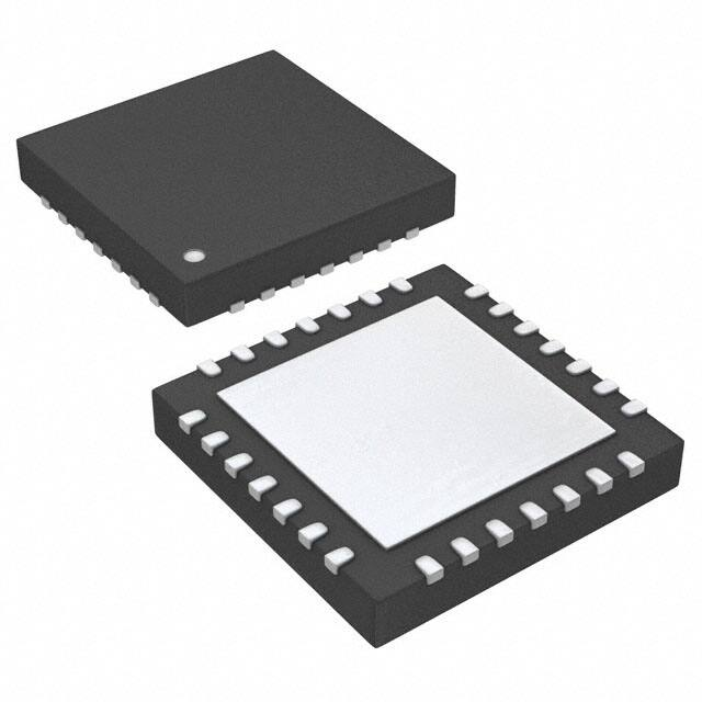
Package: QFN-28
•
Full-Color Static LED Displays for Building
Wall
Long Distance and Large Area Illumination
DESCRIPTION
The TLC5970 is a three-channel, constant-current
sink driver with a buck dc/dc converter and a
differential signal interface. Each channel has
individually adjustable currents with 4096 PWM
grayscale (GS) steps and 128 constant-current sink
steps for dot correction (DC). The dot correction
adjusts the brightness variations between LEDs. The
DC data can be stored in the internal EEPROM. Also,
current through all three channels can be controlled
by global brightness control (BC) data with 128 steps.
GS control, DC, and BC are accessible via a
differential signal interface. The maximum current
value for each channel is set by a single external
resistor. The TLC5970 contains a dc/dc buck
converter. The dc/dc converter improves system
efficiency, reduces system level currents, and allows
thinner gauge wiring by optimizing the LED anode
voltage to keep the LED cathode voltage to 1 V. The
TLC5970 proivdes overtemperature protection by
turning all output drivers off when the IC temperature
is too high (exceeds +138°C).
VCC
Power
Supply
GND
GND
VCC
SWOFF
0.01 mF
VREG
0.1 mF
PH
BOOT
VREGIF
FB
GND
0.01 mF
0.1 mF
IREF2
Controller
Open
SDTY
SDTZ
SDKY
SDKZ
VCC
SWOFF
0.01 mF
VREG
PH
0.01 mF
BOOT
VREGIF
FB
IREF2
IREF1
OUT2
IREF1
OUT2
IREF0
OUT1
IREF0
OUT1
VROM
OUT0
VROM
OUT0
SDTA
SDTY
SDTA
SDTY
SDTB
SDTZ
SDTB
SDTZ
SCKA
SCKY
SCKA
SCKY
SCKB
SCKZ
SCKB
SCKZ
TLC5970
Open
TLC5970
Typical Application Circuit Example
1
2
Please be aware that an important notice concerning availability, standard warranty, and use in critical applications of Texas
Instruments semiconductor products and disclaimers thereto appears at the end of this data sheet.
All trademarks are the property of their respective owners.
PRODUCTION DATA information is current as of publication date.
Products conform to specifications per the terms of the Texas
Instruments standard warranty. Production processing does not
necessarily include testing of all parameters.
Copyright © 2010, Texas Instruments Incorporated
�TLC5970
SBVS140A – MARCH 2010 – REVISED MAY 2010
www.ti.com
This integrated circuit can be damaged by ESD. Texas Instruments recommends that all integrated circuits be handled with
appropriate precautions. Failure to observe proper handling and installation procedures can cause damage.
ESD damage can range from subtle performance degradation to complete device failure. Precision integrated circuits may be more
susceptible to damage because very small parametric changes could cause the device not to meet its published specifications.
ORDERING INFORMATION (1)
(1)
PRODUCT
PACKAGE-LEAD
TLC5970
QFN-28 6.0 mm × 6.0 mm
ORDERING NUMBER
TRANSPORT MEDIA,
QUANTITY
TLC5970RHPR
Tape and Reel, 3000
TLC5970RHPT
Tape and Reel, 250
For the most current package and ordering information, see the Package Option Addendum at the end of this document, or visit the
device product folder at ti.com.
ABSOLUTE MAXIMUM RATINGS (1) (2)
Over operating free-air temperature range, unless otherwise noted.
VALUE
Supply voltage
Input voltage
MAX
VCC
–0.3
+40
V
BOOT
–0.3
+50
V
BOOT-PH difference
–0.3
+10
V
FB
–0.3
+18
V
IREF0 to IREF2, SWOFF
–0.3
VREG + 0.3
V
SDTA, SDTB, SCKA, SCKB
–10
+15
V
VROM
–0.3
+21
V
PH (steady-state)
–0.6
+40
V
–1.2
V
PH (transient < 10 ns)
Output voltage
OUT0 to OUT2
–0.3
+18
V
SDTY, SDTZ, SCKY, SCKZ
–10
+15
V
VREG, VREGIF
–0.3
+6
V
PH (dc)
Output current
–800
PH (peak)
–2
OUT0 to OUT2
SDTY, SDTZ, SCKY, SCKZ
Electrostatic discharge rating
–35
mA
mA
4
kV
Human body model (HBM) Other pins
2
kV
1000
V
Charged device model (CDM) SDTA, SDTB, SCKA, SCKB,
SDTY, SDTZ, SCKY, SCKZ
TJ
Storage temperature
Tstg
2
A
+180
+35
Charged device model (CDM) Other pins
(2)
mA
Human body model (HBM) SDTA, SDTB, SCKA, SCKB,
SDTY, SDTZ, SCKY, SCKZ
Operation junction temperature
(1)
UNIT
MIN
(max)
–55
500
V
+150
°C
+150
°C
Stresses beyond those listed under absolute maximum ratings may cause permanent damage to the device. These are stress ratings
only, and functional operation of the device at these or any other conditions beyond those indicated under recommended operating
conditions is not implied. Exposure to absolute-maximum-rated conditions for extended periods may affect device reliability.
All voltage values are with respect to network ground terminal.
Submit Documentation Feedback
Copyright © 2010, Texas Instruments Incorporated
Product Folder Link(s): TLC5970
�TLC5970
www.ti.com
SBVS140A – MARCH 2010 – REVISED MAY 2010
THERMAL INFORMATION
TLC5970
THERMAL METRIC (1)
RHP
UNITS
28
qJA
Junction-to-ambient thermal resistance
26.7
qJC(top)
Junction-to-case(top) thermal resistance
11.7
qJB
Junction-to-board thermal resistance
5.3
yJT
Junction-to-top characterization parameter
0.4
yJB
Junction-to-board characterization parameter
5.2
qJC(bottom)
Junction-to-case(bottom) thermal resistance
1.6
(1)
°C/W
For more information about traditional and new thermal metrics, see the IC Package Thermal Metrics application report, SPRA953.
DISSIPATION RATINGS
(1)
PACKAGE
DERATING FACTOR
ABOVE TA = +25°C
POWER RATING
TA < +25°C
POWER RATING
TA = +70°C
POWER RATING
TA = +85°C
QFN-28
Bottom side heat sink soldered (1)
33.2 mW/°C
4149 mW
2655 mW
2157 mW
The package thermal impedance is calculated in accordance with JESD51-5.
Submit Documentation Feedback
Copyright © 2010, Texas Instruments Incorporated
Product Folder Link(s): TLC5970
3
�TLC5970
SBVS140A – MARCH 2010 – REVISED MAY 2010
www.ti.com
RECOMMENDED OPERATING CONDITIONS
At TA = –40°C to +85°C, unless otherwise noted.
TLC5970
MIN
NOM
MAX
UNIT
DC CHARACTERISTICS
VCC
Supply voltage
VCC1
VI
VCC = SWOFF = VREG = VREFIF = FB
(no buck conver operation mode)
FB (buck converter operation mode)
VI1
Voltage at input terminal
VI2
SDTA, SDTB, SCKA, SCKB
10
36
V
4.75
5.5
V
7
17
V
–7
12
V
19.5
V
VROM for data writing
18.5
19
–12
12
V
VID
Differential voltage at input terminal (1)
SDTA-SDTB, SCKA-SCKB
VIH
High level input voltage
SWOFF
0.7 × VREG
VREG
V
VIL
Low level input voltage
SWOFF
GND
0.3 × VREG
V
VO
Voltage at output terminal
OUT0 to OUT2
17
V
IOLC
Constant output sink current
OUT0 to OUT2
150
mA
IOH
High level output current
SDTY, SDTZ, SCKY, SCKZ
IOL
Low level output current
SDTY, SDTZ, SCKY, SCKZ
TA
Operating free-air temperature
TJ
Operating junction temperature
–30
mA
30
mA
–40
+85
°C
–40
+125
°C
AC CHARACTERISTICS
fCLK
Data shift clock frequency
SCKA-SCKB
TWH/TWL
Pulse duration
SCKA-SCKB
TSU
Setup time
TH
NROM
(1)
4
20
MHz
12
ns
(SDTA-SDTB)-(SCKA-SCKB) ↑
5
ns
Hold time
(SDTA-SDTB)-(SCKA-SCKB) ↑
3
Number of EEPROM write cycles
At each address
ns
10
Times
Differential input voltage is measured at the noninverting terminal with respect to the inverting terminal.
Submit Documentation Feedback
Copyright © 2010, Texas Instruments Incorporated
Product Folder Link(s): TLC5970
�TLC5970
www.ti.com
SBVS140A – MARCH 2010 – REVISED MAY 2010
ELECTRICAL CHARACTERISTICS
At VCC = 10 V to 36 V and TA = –40°C to +85°C. Typical values at VCC = 24 V, FB = 17 V, and TA = +25°C, unless otherwise
noted.
TLC5970
PARAMETER
TEST CONDITIONS
MIN
TYP
MAX
UNIT
300
770
MΩ
BUCK DC/DC CONVERTER BLOCK
RDSON
High-side MOS switch on-resistance
At PH pin. VCC = 10 V to 36V, IO = 500mA,
VBOOT = VCC + 9 V,
PH high-side MOS switch is on
RDSOFF
High-side MOS switch off-resistance
At PH pin. VCC = 36 V, PH = 0 V,
PH high-side MOS switch is off
1
MΩ
At BOOT pin. VCC = 10 V, IBOOT = –10 mA,
PH high-side MOS switch is off
8
V
VBOOT
Boot regulator output voltage
VBOOT1
VSCP
Short-circuit protection detection
At BOOT pin. VCC = 36 V, PH = 0 V,
IBOOT = no load,
PH high-side MOS switch is off
3.75
V
V
4
4.25
IFB
At FB pin. SDTA/SCKA = 0 V, SDTB/SCKB = 3 V,
SDTY/SDTZ/SCKY/SCKZ/PH/BOOT = open,
FB = 7 V to 17 V, VOUTn = 1.0 V, GSn = 000h,
DCn = BC = 7Fh, RIREF = 15 kΩ,
internal oscillator mode, and auto repeat mode
18
29
mA
IFB1
At FB pin. SDTA/SCKA = 0 V, SDTB/SCKB = 3 V,
SDTY/SDTZ/SCKY/SCKZ/PH/BOOT = open,
FB = 7 V to 17 V, VOUTn = 1.0 V, GSn = 000h,
DCn = BC = 7Fh, RIREF = 2 kΩ,
internal oscillator mode, and auto repeat mode
19
30
mA
IFB2
At FB pin. SDTA/SDTB = 10 MHz,
SCKA/SCKB = 20 MHz with 0 V to 3 V swing,
SDTY-SDTZ/SCKY-SCKZ = RLDIF = 10 kΩ,
CLDIF = 15 pF, PH/BOOT = open, FB = 7 V to 17 V,
VOUTn = 1.0 V, GSn = FFFh, DCn = BC = 7Fh,
RIREF = 2 kΩ, internal oscillator mode,
and auto repeat mode
36
60
mA
IFB3
At FB pin. SDTA/SDTB = 10 MHz,
SCKA/SCKB = 20 MHz with 0 V to 3 V swing,
SDTY-SDTZ/SCKY-SCKZ = RLDIF = 2 × 51 Ω,
CLDIF = 50 pF, PH/BOOT = open, FB = 7 V to 17 V,
VOUTn = 1.0 V, GSn = FFFh, DCn = BC = 7Fh,
RIREF = 2 kΩ, internal oscillator mode,
and auto repeat mode
65
115
mA
IFB4
At FB pin. SDTA/SDTB = 10 MHz,
SCKA/SCKB = 20 MHz with 0 V to 3 V swing,
SDTY-SDTZ/SCKY-SCKZ = RLDIF = 2 × 51 Ω,
CLDIF = 50 pF, PH/BOOT = open, FB = 7 V to 17 V,
VOUTn = 1.0 V, GSn = FFFh, DCn = BC = 7Fh,
RIREF = 1 kΩ, internal oscillator mode,
and auto repeat mode
68
130
mA
Input current
At FB pin
10
Submit Documentation Feedback
Copyright © 2010, Texas Instruments Incorporated
Product Folder Link(s): TLC5970
5
�TLC5970
SBVS140A – MARCH 2010 – REVISED MAY 2010
www.ti.com
ELECTRICAL CHARACTERISTICS (continued)
At VCC = 10 V to 36 V and TA = –40°C to +85°C. Typical values at VCC = 24 V, FB = 17 V, and TA = +25°C,
unless otherwise noted.
TLC5970
PARAMETER
TEST CONDITIONS
MIN
TYP
MAX
UNIT
136
151
166
mA
0.1
µA
LED DRIVER BLOCK
IOLC
Constant output current
At OUT0 to OUT2 pins. OUTn are on,
DCn = BC = 7Fh,
VOUT = 1 V, RIREF = 1 kΩ
IOLKG
Leakage output current
At OUT0 to OUT2 pins. OUTn are off, DCn = 7Fh,
BC = 7Fh, VOUT = 17 V, RIREF = 1 kΩ
ΔIOLC
Constant-current error
(channel-to-channel) (1)
At OUT0 to OUT2 pins. OUTn are on,
DCn = BC = 7Fh,
VOUT = 1 V, RIREF = 1 kΩ
±0.5
±3
%
ΔIOLC1
Constant-current error
(device-to-device) (2)
At OUT0 to OUT2 pins. OUTn are on,
DCn = BC = 7Fh,
VOUT = 1 V, RIREF = 1 kΩ
±3
±6
%
ΔIOLC2
Line regulation (3)
OUT0 to OUT2 are on, DCn = BCn = 7Fh,
VOUT = 1 V, RIREF = 1 kΩ, VREG = 3.3 V to 5.5 V
±0.5
±2
%/V
ΔIOLC3
Load regulation (4)
OUT0 to OUT2 are on, DCn = BCn = 7Fh,
VOUT = 1 V to 3 V, RIREF = 1 kΩ
±1
±2
%/V
VIREF
Reference voltage output
IREF0 to IREF2, RIREF = 1 kΩ
1.20
1.23
(1)
1.17
V
The deviation of each output from the average of OUT0–OUT2 constant-current. Deviation is calculated by the formula:
IOUTn
D (%) =
-1
´ 100
(IOUT0 + IOUT1 + IOUT2)
3
(2)
The deviation of the OUT0–OUT2 constant-current average from the ideal constant-current value.
Deviation is calculated by the following formula:
(IOUT0 + IOUT1 + IOUT2)
3
D (%) =
- (Ideal Output Current)
´ 100
Ideal Output Current
Ideal current is calculated by the formula:
IOUT(IDEAL) = 125 ´
(3)
1.20
RIREF
Line regulation is calculated by this equation:
D (%/V) =
(IOUTn at VREG = 5.5 V) - (IOUTn at VREG = 3 V)
(IOUTn at VREG = 3.0 V)
(4)
5.5 V - 3 V
Load regulation is calculated by the equation:
D (%/V) =
(IOUTn at VOUTn = 3 V) - (IOUTn at VOUTn = 1 V)
100
´
(IOUTn at VOUTn = 1 V)
6
100
´
3V-1V
Submit Documentation Feedback
Copyright © 2010, Texas Instruments Incorporated
Product Folder Link(s): TLC5970
�TLC5970
www.ti.com
SBVS140A – MARCH 2010 – REVISED MAY 2010
ELECTRICAL CHARACTERISTICS (continued)
At VCC = 10 V to 36 V and TA = –40°C to +85°C. Typical values at VCC = 24 V, FB = 17 V, and TA = +25°C,
unless otherwise noted.
TLC5970
PARAMETER
TEST CONDITIONS
MIN
TYP
MAX
UNIT
DIFFERENTIAL INTERFACE BLOCK
VITP
Positive-going input threshold
voltage
At SDTA-SDTB or SCKA-SCKB pins. Common-mode,
VIB = 1.5 V (see Figure 4)
VITN
Negative-going input threshold
voltage
At SDTA-SDTB or SCKA-SCKB pins. Common-mode,
VIB = 1.5 V (see Figure 4)
VITHYS
Hysteresis voltage (|VITP – VITN|)
Common-mode
0.2
–0.2
V
50
110
mV
II
At SDTA/SDTB/SCKA/SCKB pins. VIH = 12 V
(other inputs at 0 V), VCC = 24 V
2
3
mA
II1
At SDTA/SDTB/SCKA/SCKB pins. VIH = 12 V
(other inputs at 0 V), VCC = 0 V
2
3
mA
Input current
30
V
II2
At SDTA/SDTB/SCKA/SCKB pins. VIH = –7 V
(other inputs at 0 V), VCC = 24 V
–3
–1.2
mA
II3
At SDTA/SDTB/SCKA/SCKB pins. VIH = –7 V
(other inputs at 0 V), VCC = 0 V
–3
–1
mA
1.8
VOD
Differential output voltage
At SDTY-SDTZ or SCKY-SCKZ pins.
1/2 × RLDIF = 51 Ω (see Figure 6)
1
ΔVOD
Change in magnitude of differential
output voltage (5)
At SDTY-SDTZ or SCKY-SCKZ pins.
1/2 × RLDIF = 51 Ω (see Figure 6)
–0.2
VOC
Steady-state common-mode output
voltage
At SDTY-SDTZ or SCKY-SCKZ pins.
1/2 × RLDIF = 51 Ω (see Figure 6)
1.5
ΔVOC
Change in magnitude of steady-state
common-mode output voltage (5)
At SDTY-SDTZ or SCKY-SCKZ pins.
1/2 × RLDIF = 51 Ω (see Figure 6)
–0.2
RINT
Internal resistor between differential
input pair
At SDTA-SDTB or SCKA-SCKB pins.
A pins = 0 V, B pins = 1.8 V
IO
Output current with power off
At SDTY-SDTZ or SCKY-SCKZ pins. VCC = 0 V,
–7 V ≤ SDTY/SDTZ/SCKY/SCKZ ≤ 12 V, 1 pin sweep,
all other outputs are open
(5)
VREG/2
3
V
0.2
V
3
V
0.2
V
10
–10
±1
kΩ
20
µA
ΔVOD and ΔVOC are the changes in the steady-state magnitude of VOD and VOC, respectively, that occur when the output data change
from a high level to a low level.
Submit Documentation Feedback
Copyright © 2010, Texas Instruments Incorporated
Product Folder Link(s): TLC5970
7
�TLC5970
SBVS140A – MARCH 2010 – REVISED MAY 2010
www.ti.com
ELECTRICAL CHARACTERISTICS (continued)
At VCC = 10 V to 36 V and TA = –40°C to +85°C. Typical values at VCC = 24 V, FB = 17 V, and TA = +25°C,
unless otherwise noted.
TLC5970
PARAMETER
TEST CONDITIONS
MIN
TYP
MAX
UNIT
At VREG pin. CREG = 0.01 µF, GSn = 000h
4.75
5.0
5.25
V
At VREGIF pin. CREG1 = 0.1 µF, RLDIF = 2 × 51 Ω
4.75
5.0
5.25
V
WHOLE BLOCK
VREG
VREG1
Internal power-supply voltage
VSTR
Undervoltage lockout
At VREG pin, VREG rising
3.8
4.1
4.4
V
VHYS
Undervoltage lockout hysteresis
At VREG pin
250
350
450
mV
ICC
At VCC pin. SDTA/SCKA = 0 V, SDTB/SCKB = 3 V,
SDTY/SDTZ/SCKY/SCKZ/PH/BOOT = open,
PH not switching, VOUTn = 1.0 V, GSn = 000h,
DCn = BC = 7Fh, RIREF = 15 kΩ,
internal oscillator mode, and auto repeat mode
4.0
7.5
mA
ICC1
At VCC pin. SDTA/SCKA = 0 V, SDTB/SCKB = 3 V,
SDTY/SDTZ/SCKY/SCKZ/PH/BOOT = open,
PH not switching, VOUTn = 1.0 V, GSn = 000h,
DCn = BC = 7Fh, RIREF = 2 kΩ,
internal oscillator mode, and auto repeat mode
7.5
10
mA
ICC2
At VCC pin. SDTA/SDTB = 10 MHz,
SCKA/SCKB = 20 MHz with 0 V to 3 V swing,
SDTY-SDTZ/SCKY-SCKZ = RLDIF = 10 kΩ,
CLDIF = 15 pF, PH/BOOT = open, PH is full switching,
VOUTn = 1.0 V, GSn = FFFh, DCn = BC = 7Fh,
RIREF = 2 kΩ, internal oscillator mode,
and auto repeat mode
8.5
25
mA
ICC3
At VCC pin. SDTA/SDTB = 10 MHz,
SCKA/SCKB = 20 MHz with 0 V to 3 V swing,
SDTY-SDTZ/SCKY-SCKZ = RLDIF = 2 × 51 Ω,
CLDIF = 50 pF, PH/BOOT = open, PH is full switching,
VOUTn = 1.0 V, GSn = FFFh,
DCn = BC = 7Fh, RIREF = 2 kΩ,
internal oscillator mode, and auto repeat mode
8.5
25
mA
ICC4
At VCC pin. SDTA/SDTB = 10 MHz,
SCKA/SCKB = 20 MHz with 0 V to 3 V swing,
SDTY-SDTZ/SCKY-SCKZ = RLDIF = 2 × 51 Ω,
CLDIF = 50 pF, PH/BOOT = open, PH is full switching,
VOUTn = 1.0 V, GSn = FFFh,
DCn = BC = 7Fh, RIREF = 1 kΩ,
internal oscillator mode, and auto repeat mode
15
35
mA
Supply current
II4
Input current
II5
At SWOFF pin. VIH = +5 V, VIL = GND
TTSD
Thermal shutdown trip point
Rising junction temperature (6)
THYST
Thermal shutdown hysteresis
Junction temperature (6)
TPTD
Pre thermal shutdown trip point
Rising junction temperature
THYSP
Pre thermal shutdown hysteresis
Junction temperature (6)
(6)
8
–2
1000
µA
5
10
mA
+150
+162
+175
°C
+5
+10
+20
°C
+125
+138
+150
°C
+4
+8
+16
°C
At VROM pin. VIH = +19.0 V
(6)
Not tested, specified by design.
Submit Documentation Feedback
Copyright © 2010, Texas Instruments Incorporated
Product Folder Link(s): TLC5970
�TLC5970
www.ti.com
SBVS140A – MARCH 2010 – REVISED MAY 2010
SWITCHING CHARACTERISTICS
At VCC = 10 V to 36 V, TA = –40°C to +85°C, RIREF = 1 kΩ, and VLED = 5.0 V. Typical values at VCC = 24 V and TA = +25°C,
unless otherwise noted.
TLC5970
PARAMETER
tR0
Rise time
TEST CONDITIONS
TYP
At SDTY, SDTZ, SCKY, or SCKZ pins. RLDIF = 2 × 51 Ω,
CLDIF = 50 pF, SDTA-SDTB = SCKA-SCKB = 20 MHz,
measured at 0.4 V differential point
(see Figure 10 and Figure 11)
tR1
At OUTn pins. DCn/BC = 7Fh, RLLED = 27 Ω, CLLED = 15 pF
(see Figure 12)
tF0
At SDTY, SDTZ, SCKY, or SCKZ pins. RLDIF = 2 × 51 Ω,
CLDIF = 50 pF, SDTA-SDTB = SCKA-SCKB = 20 MHz,
measured at 0.4 V differential point
(see Figure 10 and Figure 11)
Fall time
MIN
MAX
UNIT
15
ns
15
ns
15
ns
10
35
ns
10
tF1
At OUTn pins. DCn/BC = 7Fh, RLLED = 27 Ω, CLLED = 15 pF
(see Figure 12)
tD0
(SCKA-SCKB)↑ – (SDTY-SDTZ) , RLDIF = 2 × 51 Ω,
CLDIF = 50 pF, DSI mode = 2 (see Figure 10)
20
30
60
ns
tD0A
(SCKA-SCKB)↑ – (SDTY-SDTZ) , RLDIF = 2 × 51 Ω,
CLDIF = 50 pF, DSI mode = 1 (see Figure 10)
30
50
90
ns
tD0B
(SCKA-SCKB) ↓ – (SDTY-SDTZ) , RLDIF = 2 × 51 Ω,
CLDIF = 50 pF, DSI mode = 0 (see Figure 11)
20
30
55
ns
tD1
(SCKA-SCKB)↑ – (SCKY-SCKZ)↑, RLDIF = 2 × 51 Ω,
CLDIF = 50 pF, DSI mode = 2 (see Figure 10)
13
19
33
ns
(SCKA-SCKB)↑ – (SCKY-SCKZ)↑, RLDIF = 2 × 51 Ω,
CLDIF = 50 pF, DSI mode = 1 (see Figure 10)
13
19
33
ns
tD1B
(SCKA-SCKB)↑↓ – (SCKY-SCKZ)↑↓, RLDIF = 2 × 51 Ω,
CLDIF = 50 pF, DSI mode = 0 (see Figure 11)
13
20
30
ns
tD2 (1)
(SCKY-SCKZ)↑ – (SDTY-SDTZ), RLDIF = 2 × 51 Ω,
CLDIF = 50 pF, DSI mode = 2
5
11
30
ns
tD2A (1)
(SCKY-SCKZ)↑ – (SDTY-SDTZ), RLDIF = 2 × 51 Ω,
CLDIF = 50 pF, DSI mode = 1
15
31
60
ns
tD3
(SCKA-SCKB) ↑ – OUT0 turns on/off (see Figure 12)
12
30
60
ns
tD4
(SCKA-SCKB) ↑ – OUT1 turns on/off (see Figure 12)
35
70
140
ns
tD5
(SCKA-SCKB) ↑ – OUT2 turns on/off (see Figure 12)
55
110
220
ns
tW
Shift clock output
one pulse width
(SCKY-SCKZ)↑ – (SCKY-SCKZ) ↓ with DSI mode 1 or mode 2
(see Figure 10)
12
25
35
ns
tW_ERR
Shift clock output
pulse width error
High-level pulse width of (SCKA-SCKB) – high-level pulse
width of (SCKY-SCKZ) with DSI mode 0 (see Figure 11)
10
ns
fOSC
Internal oscillator frequency
fSW
High-side MOS switching
maximum frequency
tD1A
Propagation delay time
tDTY0
tDTY1
tSCP
(1)
On-duty cycle
Short-circuit detection time
–10
8
10
12
MHz
1
1.25
1.5
MHz
At PH pin. EEPROM data = 7h
83
86
90
%
At PH pin. EEPROM data = 0h
15
18
21
%
2.4
4.0
µs
At PH pin
VFB < VSCP
The propagation delays are calculated by tD2 = tD0 – tD1, tD2A = tD0A – tD1A.
Submit Documentation Feedback
Copyright © 2010, Texas Instruments Incorporated
Product Folder Link(s): TLC5970
9
�TLC5970
SBVS140A – MARCH 2010 – REVISED MAY 2010
www.ti.com
FUNCTIONAL BLOCK DIAGRAM
VCC
VCC
FB
OVP/SCP
FB
VREG
BOOT
Voltage
Reference
Voltage Control
with Soft-Start,
Overvoltage Protection,
and Short-Circuit Protection
SWOFF
Switch
Timing
Control
FB
5-V
Regulator
PH
PH
High-Side
MOS SW
10-MHz
OSC
VREG
OUT 0
1/2
CLK
SEL
Display
Timing
Control
VREG
OUT 1
Constant-Current
Control
OUT 2
CLKSEL
UVLO
DSPRST
36
AUTORPT
Thermal
Detector
7
21
BC Data
LSB
VROM
IREF0
MSB
ROM Write
Control
LSB
7
IREF1
DC
Data
7-Bit Brightness
Control Second Latch
3
IREF2
GS
Data
MSB
12-Bit Function Control
Data Latch
8
EEPROM
(36-Bit)
29
0
LSB
13
DC
Loadcnt
11
MSB
VCC FB
21-Bit Dot Correction
Data Latch
TIMESEL
0
Latch
Pulse Gen
LSB
20
21
Select
Switch
MSB
36-Bit Grayscale
Second Data Latch
Address/Command
0
36
LSB
Differential
Line Receiver
0
SCKB
3
MSB
40-Bit Common Shift Register
SDTB
SCKA
Differential
Line Driver
35
LSB
Clock
Timing
Adjust
0
VREGIF
MSB
36-Bit Grayscale
First Data Latch
19
SDTA
5-V
Regulator
35
SDTY
SDTZ
39
SCKY
SCKZ
GND
10
Submit Documentation Feedback
Copyright © 2010, Texas Instruments Incorporated
Product Folder Link(s): TLC5970
�TLC5970
www.ti.com
SBVS140A – MARCH 2010 – REVISED MAY 2010
PIN CONFIGURATIONS
VCC
NC
PH
24
23
22
(1)
GND
26
NC
SWOFF
27
25
VREG
28
RHP PACKAGE
QFN-28
(TOP VIEW)
VREGIF
1
21
BOOT
IREF2
2
20
FB
IREF1
3
19
OUT2
18
OUT1
Thermal Pad
(Bottom Side)
14
SDTZ
NC
15
13
7
SCKY
SDTB
12
SDTY
SCKZ
16
11
6
NC
SDTA
10
OUT0
SCKB
17
9
5
SCKA
VROM
8
4
NC
IREF0
(1) NC = not connected
Submit Documentation Feedback
Copyright © 2010, Texas Instruments Incorporated
Product Folder Link(s): TLC5970
11
�TLC5970
SBVS140A – MARCH 2010 – REVISED MAY 2010
www.ti.com
TERMINAL FUNCTIONS
TERMINAL
NAME
PIN NO.
I/O
SDTA
6
I
Noninverting serial data input
SDTB
7
I
Inverting serial data input
SCKA
9
I
Noninverting data shift clock input. All data in the Common Shift Register are shifted to the MSB side by 1
bit and synchronized to the rising edge of the differential clock generated by SCKA and SCKB. The
differential data made by SDTA and SDTB are shifted into the Common Shift Register LSB at the same
time.
SCKB
10
I
Inverting data shift clock input. All data in the shift register are shifted to the MSB side by 1 bit
synchronized to the rising edge of the differential clock generated by SCKA and SCKB. The differential
data made by SDTA and SDTB are shifted into the Common Shift Register LSB at the same time.
SDTY
16
O
Noninverting serial data output
SDTZ
15
O
Inverting serial data output
SCKY
13
O
Noninverting serial data shift clock output
SCKZ
12
O
Inverting serial data shift clock output
SWOFF
27
I
Disable buck converter. When SWOFF is connected to VREG, the buck converter is not operated and the
OVP/SCP flag is not set even if the device is in an error condition. When SWOFF is low, the buck
converter is operated. This terminal is internally pulled down to GND by approximately a 10 kΩ resistor.
VROM
5
IREF0
4
I/O
IREF1
3
I/O
IREF2
2
I/O
OUT0
17
O
OUT1
18
O
OUT2
19
O
VREG
28
O
Internal regulator output. This pin requires a 0.01 µF decoupling capacitor to ground. This output cannot
be used for any other function and no current can be pulled from this output.
VREGIF
1
O
Internal regulator output for the differential interface circuit. This pin requires a 0.1 µF decoupling
capacitor. This output cannot be used for any other function and no current can be pulled from this
output.
FB
20
I
Feedback voltage input for the converter and power-supply for differential signal interface output and LED
driver. Connect this pin to the dc/dc converter output voltage. The FB pin must not be opened, otherwise
higher voltage than the absolute maximum voltage is generated.
PH
22
O
Source of the high-side power MOSFET. Connected to an external inductor and diode.
BOOT
21
I/O
Boost capacitor for the high-side power MOSFET gate driver. A capacitor is connected between BOOT
and PH.
VCC
24
—
Power-supply voltage
26
—
Power ground
GND
Thermal
pad
12
EEPROM writing power supply. When this pin level is 19 V, EEPROM can be programmed for dot
correction data. This pin must be open in normal operation. This terminal is pulled down to GND by
approximately a 10 kΩ resistor internally.
8, 11, 14,
23, 25
NC
—
DESCRIPTION
The resistors connected from IREF0, IREF1, and IREF2 to GND set the maximum sink current for OUT0,
OUT1, and OUT2, respectively.
Constant-current sink output. Multiple outputs can be tied together to increase the constant-current
capability.
No internal connection. These pins are not electrically connected to the IC. They should be soldered to
the PCB. Connecting these pins to ground provides improved thermal performance.
—
The RHP package thermal pad is electrically connected to ground inside the package. This pad must be
connected to the ground plane on the PCB for best thermal performance and for mechanical reasons.
This pad cannot be connected to any other voltage other than ground. See the mechanical drawings at
the end of this document for more information.
Submit Documentation Feedback
Copyright © 2010, Texas Instruments Incorporated
Product Folder Link(s): TLC5970
�TLC5970
www.ti.com
SBVS140A – MARCH 2010 – REVISED MAY 2010
PARAMETRIC MEASUREMENT INFORMATION
PIN EQUIVALENT INPUT/OUTPUT SCHEMATICS
VREGIF
VREGIF
R2
R1
Input
R3
Output
R7
To
B Input
Figure 1. SDTA/SCKA
Figure 3. SDTY/SCKY, SDTZ/SCKZ
VREGIF
OUTn
R5
R4
Input
GND
Figure 4. OUT0 Through OUT2
R6
R7
To
A Input
Figure 2. SDTB/SCKB
Submit Documentation Feedback
Copyright © 2010, Texas Instruments Incorporated
Product Folder Link(s): TLC5970
13
�TLC5970
SBVS140A – MARCH 2010 – REVISED MAY 2010
www.ti.com
TEST CIRCUITS
VCC
VFB
FB
xA
VCC
High or Low
xB
VIA
GND
VIB
Figure 5. Receiver Test Circuit for SDTA/B and SCKA/B
VCC
FB
xY
VFB
1/2 RLDIF
VCC
VOD
High or Low
1/2 RLDIF
xZ
VOC
GND
Figure 6. Driver VOD and VOC Test Circuit for SDTY/Z and SCKY/Z
VCC
VFB
High or Low
FB
xY
xA
VCC
Output
RLDIF
CLDIF
(1)
xB
VIA
xZ
VIB
GND
(1) CLDIF includes probe and jig capacitance.
Figure 7. Rise/Fall Time and Propagation Delay Test Circuit for SDTY/Z and SCKY/Z
14
Submit Documentation Feedback
Copyright © 2010, Texas Instruments Incorporated
Product Folder Link(s): TLC5970
�TLC5970
www.ti.com
SBVS140A – MARCH 2010 – REVISED MAY 2010
VFB
VCC
VCC
OUTn
IREFn
RIREF
RLLED
VFB
VLED
CLLED
GND
Figure 8. Rise/Fall Time Test Circuit for OUTn
VFB
VCC
VCC
VFB
OUTn
IREFn
RIREF
OUTn
GND
VOUTn
VOUTfix
Figure 9. Constant-Current Test Circuit for OUTn
Submit Documentation Feedback
Copyright © 2010, Texas Instruments Incorporated
Product Folder Link(s): TLC5970
15
�TLC5970
SBVS140A – MARCH 2010 – REVISED MAY 2010
www.ti.com
TIMING DIAGRAMS
TSU, TH, tD0, tD0A, tD1, tD1A, tW, tR0, tF0
1V
SDTA
0V
1V
SDTB
0V
TSU
TH
1V
SCKA
0V
1V
SCKB
0V
tD0/tD0A
tD0/tD0A
SDTY
SDTZ
Output Voltage
Difference
(SDTY - SDTZ)
0.4 V
0V
-0.4 V
tR0
tD1/tD1A
tF0
SCKY
SCKZ
tW
Output Voltage
Difference
(SCKY - SCKZ)
0.4 V
0V
-0.4 V
tR0
tF0
Figure 10. Input/Output Timing 1 (DSI Mode = 1 or 2)
16
Submit Documentation Feedback
Copyright © 2010, Texas Instruments Incorporated
Product Folder Link(s): TLC5970
�TLC5970
www.ti.com
SBVS140A – MARCH 2010 – REVISED MAY 2010
TSU, TH, tD0B, tD1B, tR0, tF0
1V
SDTA
0V
1V
SDTB
0V
TSU
TH
1V
SCKA
0V
tW_SCKAB
1V
SCKB
0V
SDTY
tD0B
tD0B
SDTZ
Output Voltage
Difference
(SDTY - SDTZ)
0.4 V
0V
-0.4 V
tR0
tF0
tD1B
tD1B
SCKY
tW_SCKYZ
SCKZ
Output Voltage
Difference
(SCKY - SCKZ)
0.4 V
0V
-0.4 V
tR0
tF0
(1) tW_ERR = tW_SCKYZ – tW_SCKAB.
Figure 11. Input/Output Timing 2 (DSI Mode = 0)(1)
Submit Documentation Feedback
Copyright © 2010, Texas Instruments Incorporated
Product Folder Link(s): TLC5970
17
�TLC5970
SBVS140A – MARCH 2010 – REVISED MAY 2010
www.ti.com
tR1, tF1, tD3, tD4, tD5
1V
SCKA
0V
1V
SCKB
0V
tD3
(tD4, tD5)
tD3
(tD4, tD5)
5V
90%
OUT0
(OUT1, OUT2)
50%
10%
1V
tF1
tR1
Figure 12. Output Timing
18
Submit Documentation Feedback
Copyright © 2010, Texas Instruments Incorporated
Product Folder Link(s): TLC5970
�TLC5970
www.ti.com
SBVS140A – MARCH 2010 – REVISED MAY 2010
TYPICAL CHARACTERISTICS
At TA = +25°C and VCC = 24 V, unless otherwise noted.
REFERENCE RESISTOR vs OUTPUT CURRENT
POWER DISSIPATION vs FREE-AIR TEMPERATURE
6000
Power Dissipation Rate (mW)
RIREF, Reference Resistor (kW)
100
15
10
7.5
2.5
3.75
1.25 1.072
1
1.875
1.5
1
0
5000
TLC5970RHB
4000
3000
2000
1000
0
10 20 30 40 50 60 70 80 90 100 110 120 130 140 150
-40
DOT CORRECTION LINEARITY
160
IO = 150 mA
TA = +25°C
VCC = +24 V
BC = 7Fh
140
140
Output Current (mA)
Output Current (mA)
IO = 120 mA
120
IO = 100 mA
100
IO = 80 mA
80
IO = 60 mA
IO = 20 mA
40
TA = +25°C, VCC = +24 V
DC = 7Fh, BC = 7Fh
IO = 10 mA
IO = 150 mA
120
IO = 100 mA
100
IO = 60 mA
80
60
40
IO = 10 mA
20
20
0
0
0
1.5
1.0
0.5
2.0
2.5
3.0
0
Output Voltage (V)
160
120
16
32
48
64
96
80
112
128
Dot Correction Data (dec)
Figure 15.
Figure 16.
GLOBAL BRIGHTNESS LINEARITY
CONSTANT-CURRENT OUTPUT VOLTAGE WAVEFORM
TA = +25°C
VCC = +24 V
DC = 7Fh
140
Output Current (mA)
100
Figure 14.
OUTPUT CURRENT vs OUTPUT VOLTAGE
60
80
60
40
Free-Air Temperature (°C)
Figure 13.
160
20
0
-20
IOLC, Output Current (mA)
CH1-SCKA
(20 MHz)
CH1 (2 V/div)
IO = 150 mA
CH2-OUT0
CH2 (2 V/div)
IO = 100 mA
100
IO = 60 mA
80
CH3 (2 V/div)
60
40
IO = 10 mA
CH4 (2 V/div)
20
IOLCMax = 150 mA
DCn = BC = 7Fh
GSn = 001h
External GS CLK
No Buck Conv Mode
SCKA/SCKB = 20MHz
CH3-OUT1
CH4-OUT2
0
0
16
32
48
64
80
96
112
128
Time (40 ns/div)
Brightness Control Data (dec)
Figure 17.
Figure 18.
Submit Documentation Feedback
Copyright © 2010, Texas Instruments Incorporated
Product Folder Link(s): TLC5970
19
�TLC5970
SBVS140A – MARCH 2010 – REVISED MAY 2010
www.ti.com
APPLICATION INFORMATION
MAXIMUM CONSTANT SINK CURRENT VALUE
The TLC5970 maximum constant sink current value for each channel, IOLCMax, is determined by an external
resistor, RIREF, placed between IREFn and GND. IREFn determines the maximum current of OUTn, where n
represents outputs 0, 1, or 2. The RIREF resistor value is calculated with Equation 1:
RIREF (kW) =
VIREF (V)
´ 125
IOLCMax (mA)
Where:
VIREF = the internal reference voltage on the IREF pin (1.20 V, typically).
(1)
IOLCMax is the largest current for each output. Each output sinks the IOLCMax current when it is turned on, the dot
correction is set to the maximum value of 7Fh (127d), and global brightness control data are 7Fh (127d). Each
output sink current can be reduced by lowering the output dot correction and brightness control values.
RIREF must be between 1 kΩ (typical) and 15 kΩ (typical) to keep IOLCMax between 10 mA and 150 mA. The
output may be unstable when IOLCMax is set lower than 10 mA. Output currents lower than 10 mA can be
achieved by setting IOLCMax to 10 mA or higher and then using dot correction and global brightness control. The
constant sink current versus external resistor, RIREF, characteristics are shown in Figure 13 and Table 1.
Table 1. Maximum Constant Current versus External Resistor Value
IOLCMax (mA)
RIREF (kΩ, Typical)
150
1.00
140
1.07
120
1.25
100
1.50
80
1.88
60
2.50
40
3.75
20
7.50
10
15.0
DOT CORRECTION (DC) AND GLOBAL BRIGHTNESS CONTROL (BC) FUNCTION (CURRENT
CONTROL)
The TLC5970 has the capability to adjust the output current of each channel (OUT0 to OUT2) individually. This
function is called dot correction (DC). The DC data are seven bits long, which allows each channel output current
to be adjusted in 128 steps from 0% to 100% of the maximum output current, IOLCMax. The DC data are entered
into the TLC5970 via the serial interface and can be stored into the internal EEPROM. When the IC is powered
on, DC data are automatically loaded into the DC data latch from the EEPROM.
The TLC5970 also has the capability to adjust all output currents at the same time. This function is called global
brightness control (BC). The BC data are seven bits long, which allows all three output channel currents to be
adjusted in 128 steps from 0% to 100% of the maximum output current, IOLCMax. The BC data are entered into the
TLC5970 via the serial interface. The brightness control data cannot be stored into EEPROM. When IC is
powered on, BC data are automatically set to 7Fh (127d).
20
Submit Documentation Feedback
Copyright © 2010, Texas Instruments Incorporated
Product Folder Link(s): TLC5970
�TLC5970
www.ti.com
SBVS140A – MARCH 2010 – REVISED MAY 2010
Equation 2 determines each output (OUTn) sink current:
DCn
IOUTn (mA) = IOLCMax (mA) ´
127d
´
BC
127d
Where:
IOLCMax = the maximum channel current for each channel determined by RIREFn
DCn = the decimal dot correction value for each OUTn in the DC latch (DCn = 0d to 127d)
BC = the decimal brightness control value in the brightness control latch (BC = 0d to 127d)
(2)
DC, BC, and function current control data are shown in Table 2, Table 3, and Table 4, respectively.
Table 2. DC Data versus Current Ratio and Set Current Value
SET CURRENT
RATIO TO
MAXIMUM
CURRENT (%)
DC DATA
(Binary)
DC DATA
(Decimal)
DC DATA
(Hex)
BC DATA
(Hex)
150 mA IOLCMax
(mA, Typical)
10 mA IOLCMax
(mA, Typical)
000 0000
0
00
7F
0
0
0
000 0001
1
01
7F
0.8
1.18
0.08
000 0010
2
02
7F
1.6
2.36
0.16
—
—
—
—
—
—
—
111 1101
125
7D
7F
98.4
147.64
9.84
111 1110
126
7E
7F
99.2
148.82
9.92
111 1111
127
7F
7F
100.0
150.00
10.00
Table 3. BC Data versus Current Ratio and Set Current Value
SET CURRENT
RATIO TO
MAXIMUM
CURRENT (%)
BC DATA
(Binary)
BC DATA
(Decimal)
BC DATA
(Hex)
DC DATA
(Hex)
150 mA IOLCMax
(mA, Typical)
10 mA IOLCMax
(mA, Typical)
000 0000
0
00
7F
0
0
0
000 0001
1
01
7F
0.8
1.18
0.08
000 0010
2
02
7F
1.6
2.36
0.16
—
—
—
—
—
—
—
111 1101
125
7D
7F
98.4
147.64
9.84
111 1110
126
7E
7F
99.2
148.82
9.92
111 1111
127
7F
7F
100.0
150.00
10.00
Table 4. DC and BC Data versus Current Ratio and Set Current Value
BC DATA
(Hex)
DC DATA
(Hex)
SET CURRENT RATIO
TO MAXIMUM CURRENT
(%)
00
00
01
01
02
—
150 mA IOLCMax
(mA, Typical)
10 mA IOLCMax
(mA, Typical)
0
0
0
0
0.01
0
02
0.01
0.04
0
—
—
—
—
7D
7D
96.88
145.31
9.69
7E
7E
98.43
147.65
9.84
7F
7F
100.0
150.00
10.00
Submit Documentation Feedback
Copyright © 2010, Texas Instruments Incorporated
Product Folder Link(s): TLC5970
21
�TLC5970
SBVS140A – MARCH 2010 – REVISED MAY 2010
www.ti.com
GRAYSCALE (GS) FUNCTION (PWM CONTROL)
The OUTn PWM control is controlled by a 12-bit grayscale counter that is clocked on each rising edge of either
the internal oscillator or the shift clock signal generated by the differential signal, SCKA and SCKB. When bit 9 in
the Function Control Data Latch is '0', the internal oscillator drives the PWM grayscale counter. When bit 9 is '1',
SCKA and SCKB drive the grayscale counter. The OUTn that are programmed with a non-zero grayscale value
(GSn) turn on at the first rising edge of the selected clock after the internal latch pulse generation. After the
internal latch latch pulse goes high, the 12-bit grayscale counter counts the clock rising edges. Each OUTn stays
on until the grayscale counter value is larger than the output GSn value. OUTn turns off on the rising edge of the
clock.
When the IC powers up, all data in the Grayscale Data Latch are set to '0'. Therefore, GSn data must be written
into the Grayscale Data Latch to turn on OUTn. Equation 3 determines each OUTn on-time (tOUT_ON):
tOUT_ON (ns) = tGSCLK (ns) ´ GSn
Where:
tGSCLK = Twice the period of the internal oscillator frequency if the internal clock is selected. One period of
the shift clock frequency is generated by the differential signal if the external clock is selected.
GSn = the programmed grayscale value for OUTn (GSn = 0d to 4095d)
(3)
AUTO DISPLAY REPEAT
Auto display repeat, DSPRPT, allows OUTn to continuously turn on for multiple PWM cycles without the need to
continuously reprogram the PWM grayscale registers. When Auto Repeat is enabled, bit 8 in the Function
Control Data Latch is '1' and OUTn automatically turns on again at the next rising clock of the internal oscillator.
When Auto Display Repeat is disabled by setting the control bit to '0', OUTn do not turn on again until an internal
latch pulse is generated and another GS clock pulse goes high. This timing is shown in Figure 19 and Figure 20.
Table 5. GS Data versus OUTn On-Duty and OUTn On-Time
22
OUTn ON-DUTY RATIO
AGAINST MAXIMUM CODE (%)
OUTn ON-TIME WHEN 5 MHz
INTERNAL OSCILLATOR IS
SELECTED FOR GS CLOCK
(µs, Typical)
GS DATA
(Binary)
GS DATA
(Decimal)
GS DATA
(Hex)
0000 0000 0000
0
000
0
0
0000 0000 0001
1
001
0.02
0.20
0000 0000 0010
2
002
0.05
0.40
—
—
—
—
—
0111 1111 1111
2047
7FF
49.99
409.4
1000 0000 0000
2048
800
50.01
409.6
1000 0000 0001
2049
801
50.04
409.8
—
—
—
—
—
1111 1111 1101
4093
FFD
99.95
818.6
1111 1111 1110
4094
FFE
99.98
818.8
1111 1111 1111
4095
FFF
100.00
819.0
Submit Documentation Feedback
Copyright © 2010, Texas Instruments Incorporated
Product Folder Link(s): TLC5970
�TLC5970
www.ti.com
SBVS140A – MARCH 2010 – REVISED MAY 2010
SDTA
SDTB
SCKA
SCKB
Generated Shift Data
(Internal)
Generated Shift Data
(Internal)
Shift Register Bit 0
(Internal)
Shift Register Bit 1
(Internal)
Shift Register Bit 2
(Internal)
D39
D38
1
D39
D37
2
D36
3
D35
4
D6
5
D5
34
D3
D4
35
36
D2
37
D0
D1
38
39
40
D36
D35
D6
D5
D4
D3
D2
D1
D0
D39
D38
D37
D36
D7
D6
D5
D4
D3
D2
D1
D39
D38
D37
D8
D7
D6
D5
D4
D3
D2
D39
D38
Shift Register Bit 38
(Internal)
Shift Register Bit 39
(Internal)
¼
¼
D37
¼
¼
D38
D39
SDTY
SDTZ
SCKY
Latch pulse is generated with
the programmed internal latch
delay time from last rising edge
of the shift clock.
SCKZ
Latch Pulse
(Internal)
Addressed Latch Bit 0
(Internal)
D0
Addressed Latch Bit 1
(Internal)
D1
Addressed Latch Bit 2
(Internal)
D2
¼
¼
¼
¼
Addressed Latch Bit 34
(Internal)
D34
Addressed Latch Bit 35
(Internal)
D35
Figure 19. Serial Data Input/Output Timing Diagram 1
Submit Documentation Feedback
Copyright © 2010, Texas Instruments Incorporated
Product Folder Link(s): TLC5970
23
�TLC5970
SBVS140A – MARCH 2010 – REVISED MAY 2010
www.ti.com
SDTA
SDTB
SCKA
SCKB
Generated Shift Data
(Internal)
D39A D38A D37A D36A D35A
1
2
3
4
5
D6A
D5A
34
D4A
D3A
D2A
D1A
D0A
36
37
38
39
40
35
Generated Shift Data
(Internal)
Shift Register Bit 1
(Internal)
Shift Register Bit 2
(Internal)
D39A D38A D37A D36A D35A
D6A
D5A
D4A
D3A
D2A
D1A
D0A
RD1
RD0
D39A D38A D37A D36A
D7A
D6A
D5A
D4A
D3A
D2A
D1A
D2
RD2
RD1
RD0
D39A D38A D37A
D8A
D7A
D6A
D5A
D4A
D3A
D2A
RDn are the SID or
EEPROM read data.
RD4
RD3
RD2
RD1
RD0
D39A
D38A
RD5
RD4
RD3
RD2
RD1
RD0
D39A
D0
D1
D38
D37
D36
Shift Register Bit 39
(Internal)
D39
D38
D37
¼
Shift Register Bit 38
(Internal)
¼
¼
RD0
¼
Shift Register Bit 0
(Internal)
RD35 RD34 RD33
D36
RD35 RD34
SDTY
D39+
D38+ D37+ D36+
D35+
RD5+ RD4+ RD3+ RD2+ RD1+ RD0+ D39A+
SDTZ
D39-
D38-
D35-
RD5- RD4- RD3- RD2- RD1- RD0- D39A-
D37- D36-
SCKY
SCKZ
Latch Pulse
(Internal)
Addressed Latch Bit 0
(Internal)
D0
Addressed Latch Bit 1
(Internal)
D1
Addressed Latch Bit 2
(Internal)
D2
D34
Addressed Latch Bit 35
(Internal)
D35
¼
¼
¼
¼
Addressed Latch Bit 34
(Internal)
Figure 20. Serial Data Input/Output Timing Diagram 2 (SID/EEPROM Data Read)
24
Submit Documentation Feedback
Copyright © 2010, Texas Instruments Incorporated
Product Folder Link(s): TLC5970
�TLC5970
www.ti.com
SBVS140A – MARCH 2010 – REVISED MAY 2010
DIFFERENTIAL SIGNAL INTERFACE
This device has a differential signal receiver and differential signal driver. These differential components provide
very reliable, high-quality signal integrity over long distances. This integrity allows very large distances between
the display pixels without the need for additional drive circuitry. The drivers are enabled one second after the IC
powers up. A 10-kΩ resistor is internally mounted between SDTA and SDTB/SCKA and SCKB. Table 6 shows a
truth table of the differential signal interface receiver and driver.
Table 6. Differential Signal Interface Truth Table
RECEIVER (SDTA-SDTB, SCKA-SCKB)
DRIVER (SDTY-SDTZ, SCKY-SCKZ)
DIFFERENTIAL OUTPUTS
DIFFERENTIAL INPUTS
(VID = SDTA/SCKA – SDTB/SCKB)
INTERNAL INPUT DATA
VID ≥ 0.2 V
High
–0.2 V < VID < 0.2 V
Undefined
VID ≤ –0.2 V
Low
Open input
Low
DRIVER INPUT
SDTY/SCKY
SDTZ/SCKZ
Low
Low
High
High
High
Low
BUCK DC/DC CONVERTER
The buck converter operates with the Pulse Frequency Mode (PFM).The buck converter controls the LED anode
voltage to keep the LED cathode voltage to approximately 1 V for high efficiency and reduces the system
power-supply current. The LED anode voltage is controlled by the buck converter in this manner:
1. After the IC powers on, the LED anode voltage charges up to the FB voltage set by EEPROM with a
soft-start squence. The maximum time of the soft-start sequence is 800 ms.
2. The LED then turns on and comparators check the OUTn voltage when all LED are turned on at the 32nd
GSCLK. If the lowest voltage in OUT0 to OUT2 is below 0.9 V when all OUTn are on at 32nd GSCLK, the
buck converter target voltage is changed by one step to a higher voltage at the rising edge of the 33rd
GSCLK. If the lowest voltage in OUT0 to OUT2 is above 1.1 V, the buck converter target voltage changes by
one step to a lower voltage. If the lowest voltage in OUT0 to OUT2 is between 0.9 V and 1.1 V, then the
buck converter target voltage remains at the previous voltage.
3. If the highest voltage in OUT0 to OUT2 exceeds 4.0 V at the 32nd GSCLK rising edge when all OUTn are
on, then the buck converter target voltage does not change to a higher voltage side.
Parameter Selection for Buck Converter
The following steps select the parameters for the buck converter.
1. PH on-time selection:
VFB Minimum Voltage
Calculated PH On-Duty Ratio1 (%) =
´ 100
VCC Maximum Input Voltage
Where:
VFB = the number of LEDs in series × LED minimum forward voltage (VF) + 1.0 V
(4)
Select the closest and smaller number in Table12, then calculate PH on-duty ratio1 (%).
Example: VCC = 24 V (typical) and 25 V (maximum). LED forward voltage (VF) = 3.2 V (minimum) and 3.5 V
(typical). Two LEDs are connected in series.
Thus, VFB = 2 × 3.2 + 1 = 7.4 V. The PH on-duty ratio1 (%) = 7.4/25 = 29.6%. Therefore, 29% code ('1h')
should be selected for PH on-duty.
So, the selected PH on-duty in the EEPROM write data latch is 29%.
Submit Documentation Feedback
Copyright © 2010, Texas Instruments Incorporated
Product Folder Link(s): TLC5970
25
�TLC5970
SBVS140A – MARCH 2010 – REVISED MAY 2010
www.ti.com
2. Inductor value and current selection:
VFB Maximum Voltage
PH On-Duty Ratio2 (%) =
´ 100
VCC Minimum Input Voltage
(5)
Example: VCC = 23 V (minimum), 24 V (typical), and 25 V (maximum). LED forward voltage (VF) = 3.2 V
(minimum), 3.5 V (typical), and 3.8 V (maximum). Two LEDs are connected in series.
Thus, VFB = 2 × 3.8 + 1 = 8.6 V. The PH on-duty ratio 2 (%) = 8.6/23 = 37.4% in this case.
Calculate inductor peak current (mA):
IOUT + IFBn
Selected PH On-Duty
Inductor Peak Current (mA) =
´2
PH On-Duty Ratio2
h
100
Where:
IOUT (mA) = Total current of LEDs connected to OUT0/1/2.
IFBn (mA) = Maximum input current of IFB pin.
h (%) = Efficiency of TLC5970 buck converter (recommended to use 90).
(6)
Example: In case all LED currents are set to 60 mA by the 2.50-kΩ external resistor and total current is 180
mA. IFB3 in this data sheet is used when the differential interface output drives the next TLC5970 without a
resistor between SDTA/SDTB and SCKA/SCKB. Therefore:
180 + 115
´2
29
37.4
ILPK (mA) =
= 845.5 mA
90
100
(7)
A 25% margin for inductor variation is required. Thus, ILPK = 845.5 × 1.25 = 1057 mA. The maximum inductor
current should be larger than 1057 mA. However, the TLC5970 PH peak current must be less than 2 A in
any case.
3. Calculate inductor value (µH) for minimum inductor value:
1
Inductor Value (mH) = VCC Voltage (V, Minimum) ´
Maximum PH Switching Frequency (MHz, Maximum)
(8)
Selected PH On-Duty (%)
ILPH (mA) ´ 1000
(9)
Example: VCC = 23 V (minimum), 24 V (typical), and 25 V (maximum). Maximum PH switching frequency is
1.5 MHz. The selected PH on-duty ratio as calculated by Equation 4 is 29%. ILPK (mA) is 1057 mA as
calculated by Equation 6.
0.29
Therefore, the inductor value (mH) = 23 ´ 1 ´
1.5 1057 ´ 1000
0.29
= 23 ´ 0.67 ´
1057 ´ 1000
= 4.2 mH
(10)
26
Submit Documentation Feedback
Copyright © 2010, Texas Instruments Incorporated
Product Folder Link(s): TLC5970
�TLC5970
www.ti.com
SBVS140A – MARCH 2010 – REVISED MAY 2010
4. Calculate inductor peak current that should be selected:
The TLC5970 PH peak current must be less than 2 A and ILPK must not be greater than 2 A in any case.
1
Inductor Peak Current (A) = VCC (V, Maximum) ´
Maximum PH Switching Frequency (MHz, Maximum)
Selected PH On-Duty
Inductor Value (mH)


 工商网监
湘ICP备2023018690号
工商网监
湘ICP备2023018690号
