Product
Folder
Order
Now
Support &
Community
Tools &
Software
Technical
Documents
TLC6C5724-Q1
SLASEK2A – DECEMBER 2017 – REVISED AUGUST 2018
TLC6C5724-Q1 Automotive 24-Channel, Full Diagnostics, Constant-Current RGB LED
Driver
1 Features
3 Description
•
There are automotive applications for indicators and
for LCD local-dimming backlighting. For these
applications, more persons think multi-channel
constant-current LED drivers are necessary. The
requirement is to get the same intensity and color
temperature of LEDs. For system-level safety, it is
necessary that the LED drivers can sense faults.
1
•
•
•
•
•
•
•
AEC-Q100 Qualified for Automotive Applications
– Device Temperature Grade 1: –40°C to 125°C,
TA
24 Constant-Current-Sink Output Channels
– 50-mA Maximum Output Current
– 8-V Maximum Output Voltage
– 3 Output Groups: OUTRn, OUTGn, OUTBn
Output Current Adjustment
– 7-Bit Dot Correction for Each Channel
– 8-Bit Intensity Control for Each Group
Integrated PWM Grayscale Generator
– PWM Dimming for Each Individual Channel
– Adjustable Global Grayscale Mode: 12-Bit, 10Bit, 8-Bit
Protection and Diagnostics
– LED-Open Detection, LED-Short Detection,
Output Short-to-GND Detection
– Adjacent-Pin Short Detection
– Pre-Thermal Warning, Thermal Shutdown
– IREF Resistor Open- and Short-Detection and
-Protection
– Negate Bit Toggle for GCLK Error Detect and
LOD_LSD Register Error Check
– LOD_LSD Circuit Self-Test
Programmable Output Slew Rate
Output Channel Group Delay
Serial Data Interface
The TLC6C5724-Q1 device is an automotive 24channel constant-current RGB LED driver that can do
tests on the LEDs. The TLC6C5724-Q1 device
supplies a maximum of 50‑mA output current set by
an external resistor. The device has a 7-bit dot
correction with two ranges for each output. The
device also has an 8-bit intensity control for the
outputs of each color group. A 12-,10-, or 8-bit
grayscale control adjusts the intensity of each output.
The device has circuits that sense faults in the
system, including LED faults, adjacent-pin short
faults, reference-resistor faults, and more. A slew rate
control has 2 positions for adjustment to get the
largest decrease in system noise. There is an interval
between the changes of output level from one LED
group to a different one. This interval helps to
decrease the starting electrical current. The SDI and
SDO pins let more than one device be connected in
series for control through one serial interface.
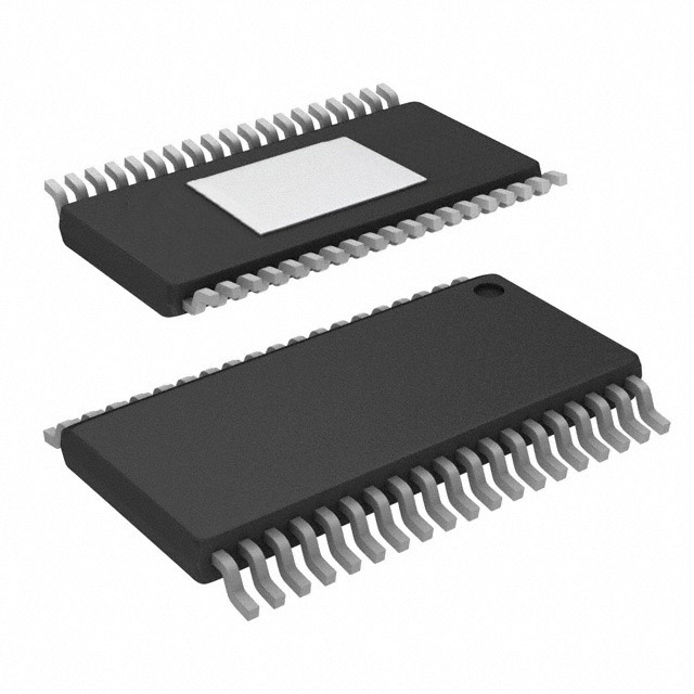
Device Information(1)
PART NUMBER
TLC6C5724-Q1
PACKAGE
BODY SIZE (NOM)
HTSSOP (38)
6.20 mm × 12.50 mm
(1) For all available packages, see the orderable addendum at
the end of the data sheet.
Typical Application Schematic
2 Applications
•
•
•
•
•
•
•
Automotive
Automotive
Automotive
Automotive
Automotive
Automotive
Automotive
Cluster
Local Dimming Display
Faceplate
HVAC Control Panel
Center Stack Display
Interior and RGB Ambient Lighting
Shift-by-Wire and Gear Shifter
VCC = 3 V - 5.5 V
SDI
SCK
VCC
LED Supply
SENSE
OUTG0
LATCH
µC
GCLK
BLANK
OUTR0
OUTB0
SDO
ERR
OUTB7
OUTR7
IREF
OUTG7
Copyright © 201 7, Texas Instrumen ts Incorpor ate d
1
An IMPORTANT NOTICE at the end of this data sheet addresses availability, warranty, changes, use in safety-critical applications,
intellectual property matters and other important disclaimers. PRODUCTION DATA.
�TLC6C5724-Q1
SLASEK2A – DECEMBER 2017 – REVISED AUGUST 2018
www.ti.com
Table of Contents
1
2
3
4
5
6
Features ..................................................................
Applications ...........................................................
Description .............................................................
Revision History.....................................................
Pin Configuration and Functions .........................
Specifications.........................................................
6.1
6.2
6.3
6.4
6.5
6.6
6.7
6.8
7
1
1
1
2
4
6
Absolute Maximum Ratings ...................................... 6
ESD Ratings.............................................................. 6
Recommended Operating Conditions....................... 6
Thermal Information .................................................. 6
Electrical Characteristics........................................... 7
Timing Requirements ................................................ 9
Switching Characteristics .......................................... 9
Typical Characteristics ............................................ 21
Detailed Description ............................................ 22
7.1 Overview ................................................................. 22
7.2 Functional Block Diagram ....................................... 22
7.3 Feature Description................................................. 23
7.4 Device Functional Modes........................................ 32
7.5 Programming .......................................................... 32
7.6 Register Maps ......................................................... 39
8
Application and Implementation ........................ 49
8.1 Application Information............................................ 49
8.2 Typical Application ................................................. 49
9 Power Supply Recommendations...................... 51
10 Layout................................................................... 51
10.1 Layout Guidelines ................................................. 51
10.2 Layout Example .................................................... 51
11 Device and Documentation Support ................. 52
11.1
11.2
11.3
11.4
11.5
Receiving Notification of Documentation Updates
Community Resources..........................................
Trademarks ...........................................................
Electrostatic Discharge Caution ............................
Glossary ................................................................
52
52
52
52
52
12 Mechanical, Packaging, and Orderable
Information ........................................................... 52
12.1 Package Option Addendum .................................. 53
4 Revision History
Changes from Original (December 2017) to Revision A
Page
•
Changed the title of the data sheet ....................................................................................................................................... 1
•
Changed items in the Features list......................................................................................................................................... 1
•
Changed the I section............................................................................................................................................................. 1
•
Changed the text of the Description section........................................................................................................................... 1
•
Changed the descriptions for the GCLK, OUTBx, OUTGx, OUTRx, SENSE, and Thermal pad rows of the Pin
Functions table ...................................................................................................................................................................... 4
•
Deleted a sentence and added a paraagraph at the end of the Grayscale Configuration section ...................................... 24
•
Changed the section title from Display Timing Reset to PWM Auto Repeat and changed the text .................................... 25
•
Changed the section title from Auto Display Repeat to PWM Timing Reset and changed the text .................................... 26
•
Deleted "and PWM" from section title "LED and PWM Diagnostics" ................................................................................... 26
•
Changed Table 1 .................................................................................................................................................................. 26
•
Changed the text following Table 1 ..................................................................................................................................... 26
•
Changed the Table 2 dolumn headers ................................................................................................................................. 26
•
Changed the Table 3 table headers and the text following the table ................................................................................... 26
•
Changed "two kinds" to "two sets" in the sentence immediately following Table 3 ............................................................ 26
•
Changed the text preceding Table 6 .................................................................................................................................... 27
•
Added a table note to Table 6 ............................................................................................................................................. 28
•
Deleted the first sentence following Table 6 ....................................................................................................................... 28
•
Changed the text and deleted two tables in the Adjacent-Pin-Short Check section ........................................................... 28
•
Added text and two tables following Table 8........................................................................................................................ 29
•
Changed the text of the IREF Short and IREF Open Detection section .............................................................................. 29
•
Changed the contents of the OUTUT column in Table 11 .................................................................................................. 29
•
Changed the text in the Pre-Thermal Warning Flag section ................................................................................................ 29
•
Changed the text in the Thermal Error Flag section ............................................................................................................ 30
•
Changed the text and deleted a diagram in the Negate Bit Toggle section......................................................................... 30
2
Submit Documentation Feedback
Copyright © 2017–2018, Texas Instruments Incorporated
Product Folder Links: TLC6C5724-Q1
�TLC6C5724-Q1
www.ti.com
SLASEK2A – DECEMBER 2017 – REVISED AUGUST 2018
Revision History (continued)
•
Changed the text and deleted a diagram in the LOD_LSD Self-Test section ..................................................................... 30
•
Changed the text in the ERROR Clear section .................................................................................................................... 31
•
Changed the text in the Global Reset section...................................................................................................................... 31
•
Changed the LED supply voltage from 7 V to 8 V in the Power Up section ........................................................................ 32
•
Added the TEF register, where the overtemperature fault is latched................................................................................... 32
•
Added a sentence to paragraph 2 of the Register Write and Read section, changed "data" to "288-bit data", and
changed "last SCK rising edge" to "288th SCK rising edge"................................................................................................ 32
•
Changed "data" to "288-bit data" in the FC-BC-DC Write section ....................................................................................... 33
•
Changed "sink current" to "APS current" and added "APS detection time" to the definition for bits 200 and 199,
respectively........................................................................................................................................................................... 33
•
Deleted two equations preceding Table 16 ......................................................................................................................... 35
•
Changed the titles of Table 16, Table 17, and Table 18 ...................................................................................................... 35
•
Added Equation 5 to calculate duty cycle............................................................................................................................. 36
•
Changed "OUTB0" to "OUTG0" for bits 167–156 in Table 19 ............................................................................................. 36
•
Changed the last sentence of the Special Command Function section............................................................................... 37
•
Changed the wording and deleted three figures in the Register Maps section ................................................................... 39
•
Changed bit numbers 287 and 286 to 277 and 276 in Figure 28 ....................................................................................... 39
•
Changed "Output slew rate" to "Output slew-rate time" for bit 203 ...................................................................................... 43
•
Changed the text in the Typical Application section............................................................................................................. 49
•
Added a sentence and a figure to the Detailed Design Procedure section ......................................................................... 50
•
Added the Application Curves section to the data sheet...................................................................................................... 50
•
Changed the LED supply voltage from 7 V to 8 V and added a sentence to the Power Supply Recommendations
section ................................................................................................................................................................................. 51
•
Added positioning information for the IREF resistor to the Layout Guidelines section ........................................................ 51
Submit Documentation Feedback
Copyright © 2017–2018, Texas Instruments Incorporated
Product Folder Links: TLC6C5724-Q1
3
�TLC6C5724-Q1
SLASEK2A – DECEMBER 2017 – REVISED AUGUST 2018
www.ti.com
5 Pin Configuration and Functions
DAP PowerPAD™ Package
38-Pin HTSSOP With Exposed Thermal Pad
Top View
SDI
1
38
SENSE
SCK
2
37
NC
LATCH
3
36
BLANK
GCLK
4
35
VCC
GCLK
5
34
IREF
GCLK
6
33
GND
OUTG0
7
32
OUTG7
OUTR0
8
31
OUTR7
OUTB0
9
30
OUTB7
OUTG1
10
29
OUTG6
Thermal
Pad
OUTR1
11
28
OUTR6
OUTB1
12
27
OUTB6
OUTG2
13
26
OUTG5
OUTR2
14
25
OUTR5
OUTB2
15
24
OUTB5
OUTG3
16
23
OUTG4
OUTR3
17
22
OUTR4
OUTB3
18
21
OUTB4
SDO
19
20
ERR
Not to scale
Pin Functions
PIN
NAME
NO.
I/O
DESCRIPTION
BLANK
36
I
Blank all outputs. BLANK low forces all channels off. Grayscale counter resets, grayscale
PWM timing controller is initialized. BLANK high starts grayscale PWM timing controller,
channels are controlled by PWM timing controller.
ERR
20
O
Open-drain error feedback
Clock input for grayscale PWM counter. The three pins are internally connected together.
GCLK
4, 5, 6
I
GND
33
—
IREF
34
I
Reference-current pin for setting the full-scale output current
Power ground
LATCH
3
I
Latch-enable input pin
NC
37
—
No internal connection
OUTB0–OUTB7
9, 12, 15, 18, 21,
24, 27, 30
O
Constant-current outputs for color group B
OUTG0–OUTG7
7, 10, 13,16, 23,
26, 29, 32
O
Constant-current outputs for color group G
4
Submit Documentation Feedback
Copyright © 2017–2018, Texas Instruments Incorporated
Product Folder Links: TLC6C5724-Q1
�TLC6C5724-Q1
www.ti.com
SLASEK2A – DECEMBER 2017 – REVISED AUGUST 2018
Pin Functions (continued)
PIN
NAME
OUTR0–OUTR7
SCK
NO.
I/O
DESCRIPTION
8, 11, 14,17, 22,
25, 28, 31
O
Constant-current outputs for color group R
2
I
Data-shift clock-input pin
SDI
1
I
Serial data-in pin
SDO
19
O
Serial data-out pin
SENSE
38
I
Connect to LED supply for LED diagnostics
VCC
35
I
Power supply pin
Thermal pad
—
—
Connect to ground to improve thermal performance
Submit Documentation Feedback
Copyright © 2017–2018, Texas Instruments Incorporated
Product Folder Links: TLC6C5724-Q1
5
�TLC6C5724-Q1
SLASEK2A – DECEMBER 2017 – REVISED AUGUST 2018
www.ti.com
6 Specifications
6.1 Absolute Maximum Ratings
over operating junction temperature range (unless otherwise noted) (1)
MIN
MAX
VCC
–0.3
6
SENSE
–0.3
8
BLANK, GCLK, LATCH, SCK, SDI
–0.3
VCC + 0.3
ERR, IREF, SDO
–0.3
VCC + 0.3
OUTR0–OUTR7, OUTG0–OUTG7,
OUTB0–OUTB7
–0.3
8
OUTR0–OUTR7, OUTG0–OUTG7,
OUTB0–OUTB7
0
50
mA
Operating junction temperature, TJ
–40
150
°C
Storage temperature, Tstg
–55
150
°C
Input voltage
Output voltage
Output current
(1)
UNIT
V
V
Stresses beyond those listed under Absolute Maximum Ratings may cause permanent damage tothedevice.Thesearestress ratings only,
which do not imply functional operation of the device attheseoranyotherconditions beyond those indicated under
RecommendedOperatingConditions. Exposuretoabsolute-maximum-ratedconditions for extended periodsmayaffect device reliability.
6.2 ESD Ratings
VALUE
Human-body model (HBM), per AEC Q100-002 (1)
V(ESD)
(1)
Electrostatic discharge
Charged-device model (CDM), per AEC
Q100-011
UNIT
±2000
All pins
±500
Corner pins (1, 19, 20,
and 38)
±750
V
AEC Q100-002 indicates that HBM stressing shallbeinaccordancewiththe ANSI/ESDA/JEDEC JS-001 specification.
6.3 Recommended Operating Conditions
over operating junction temperature range (unless otherwise noted)
MIN
NOM
UNIT
Device supply voltage
VSENSE
LED supply voltage
VO
Output voltage
VIL
Input logic-low voltage
BLANK, GCLK, LATCH, SCK, SDI
0
VIH
Input logic-high voltage
BLANK, GCLK, LATCH, SCK, SDI
0.7 VCC
VCC
V
IOH
High-level output source current
SDO
1
SDO
1
ERR
5
IOL
Low-level input sink current
IO
Constant output sink current
TA
TJ
3
MAX
VCC
OUTR0–OUTR7, OUTG0–OUTG7,
OUTB0–OUTB7
5.5
V
8
V
8
V
0.3 VCC
V
mA
mA
2
50
mA
Operating ambient temperature
–40
125
°C
Operating junction temperature
–40
150
°C
6.4 Thermal Information
TLC6C5724-Q1
THERMAL METRIC
(1)
DAP (HTSSOP)
UNIT
38 PINS
RθJA
Junction-to-ambient thermal resistance
39.6
°C/W
RθJC(top)
Junction-to-case (top) thermal resistance
31.2
°C/W
RθJB
Junction-to-board thermal resistance
18
°C/W
(1)
6
For more information about traditionalandnewthermalmetrics,see SemiconductorandICPackage ThermalMetrics .
Submit Documentation Feedback
Copyright © 2017–2018, Texas Instruments Incorporated
Product Folder Links: TLC6C5724-Q1
�TLC6C5724-Q1
www.ti.com
SLASEK2A – DECEMBER 2017 – REVISED AUGUST 2018
Thermal Information (continued)
TLC6C5724-Q1
THERMAL METRIC (1)
DAP (HTSSOP)
UNIT
38 PINS
ψJT
Junction-to-top characterization parameter
0.8
°C/W
ψJB
Junction-to-board characterization parameter
18.1
°C/W
RθJC(bot)
Junction-to-case (bottom) thermal resistance
2
°C/W
6.5 Electrical Characteristics
VCC = 3 V to 5.5 V,TJ=–40°Cto150°C,VSENSE = 5 V, GS = FFFh, BC = FFh, DC= 7Fh with upperDCrange(unlessotherwise
noted)
PARAMETER
TEST CONDITIONS
MIN
TYP
MAX
SDI, SCK, LATCH = L, BLANK = L,
GCLK = L, VOUT = 1 V, IOUT = 2 mA
4.2
5.5
SDI, SCK, LATCH = L, BLANK = L,
GCLK = L, VOUT = 1 V, IOUT = 20 mA
7.7
9
SDI, SCK, LATCH = L, BLANK = H,
GCLK = 8 MHz, VOUT = 1 V, IOUT = 20
mA , auto-repeat on
8.3
10
SDI, SCK, LATCH = L, BLANK = H,
GCLK = 8 MHz, VOUT = 1 V, IOUT = 50
mA , auto-repeat on
13.5
16
UNIT
POWER SUPPLIES
ICC
Supply current
mA
LOGIC INPUTS (SDI, SCK, LATCH, GCLK, BLANK)
IIkg
Input leakage current
Rpd
Pull down resistance at BLANK,
GCLK
At SDI, SCK, LATCH, with VI = VCC; or
at SDI, SCK, LATCH, BLANK, GCLK,
with VI = GND
–1
1
µA
250
500
750
kΩ
1.17
1.2
1.23
V
VCC
V
0.4
V
0.1 VCC
V
1
µA
CONTROL OUTPUTS (IREF, ERR, SDO)
VIREF
IREF voltage
RIREF = 0.96 kΩ
VOH
High-level output voltage
At SDO, IOH = –1 mA
VOL
Low-level output voltage
At SDO, IOL = 1 mA
VERR
ERR pin open-drain voltage
drop
IERR = 4 mA
ILKG_ERR
ERR pin leakage current
VERR = 5 V
VCC – 0.4
OUTPUT STAGE
V(OUT,min)
Minimum output voltage
K(OUT)
Ratio of output current to IREF
current, K = I(OUTx) / I(IREF)
Ilkg(OUT)
Output leakage current
VCC = 3.6 V, IOUT = 50 mA
0.67
VCC = 3 V, IOUT = 50 mA
V
0.7
40
BLANK = L, VOUT = 7 V, VSENSE = 7 V
mA/mA
0.1
µA
CHANNEL ACCURACY
I(OUT)
Constant output current
VOUT = 1 V, RIREF = 24 kΩ
1.86
2
2.14
VOUT = 1 V, RIREF = 0.96 kΩ
46.5
50
53.5
7
10
13
VOUT = 1V, RIREF open or short
Submit Documentation Feedback
Copyright © 2017–2018, Texas Instruments Incorporated
Product Folder Links: TLC6C5724-Q1
mA
7
�TLC6C5724-Q1
SLASEK2A – DECEMBER 2017 – REVISED AUGUST 2018
www.ti.com
Electrical Characteristics (continued)
VCC = 3 V to 5.5 V,TJ=–40°Cto150°C,VSENSE = 5 V, GS = FFFh, BC = FFh, DC= 7Fh with upperDCrange(unlessotherwise
noted)
PARAMETER
ΔI(Ch-Ch)
(1)
ΔI(Dev-Dev)
(2)
ΔI(Ch-Ideal)
(3)
ΔI(OUT-VCC)
(4)
ΔI(OUTVOUT
TEST CONDITIONS
TYP
MAX
Current accuracy (channel-tochannel in same color group)
–4%
4%
VOUT = 1 V, IOUT = 2 mA
–4%
4%
Current accuracy (device-todevice)
VOUT= 1 V, IOUT = 50 mA
–4%
4%
VOUT = 1 V, IOUT = 2 mA
-–4%
4%
Current accuracy (channel-toideal output)
VOUT = 1 V, IOUT = 50 mA
–7%
7%
VOUT = 1 V, IOUT = 2 mA
–7%
7%
VOUT = 1 V, VCC = 3 V to 5.5 V, IOUT =
50 mA
–0.7
0.7
VOUT = 1 V, VCC = 3 V to 5.5 V, IOUT = 2
mA
–0.7
0.7
VOUT = 1 V to 3 V, IOUT = 50 mA
–0.7
0.7
VOUT = 1 V to 3 V, IOUT = 2 mA
–0.7
0.7
Line regulation
Load regulation
(5)
MIN
VOUT = 1 V, IOUT = 50 mA
UNIT
%/V
%/V
PROTECTION CIRCUITS
VLOD1
LED open-circuit detection low
threshold
LOD_VOLTAGE = 0b
0.275
0.3
0.32
V
VLOD2
LED open-circuit detection high
threshold
LOD_VOLTAGE = 1b
0.48
0.5
0.52
V
VLSD1
LED short-circuit detection high
threshold
LSD_VOLTAGE = 0b
VSENSE –
0.4
VSENSE –
0.3
VSENSE –
0.2
V
VLSD2
LED short-circuit detection low
threshold
LSD_VOLTAGE= 1b
VSENSE –
0.8
VSENSE –
0.7
VSENSE –
0.6
V
IIREF_OC
IREF resistor open-circuit
detection threshold
VCC = 5 V
8
10
12
µA
IIREF_OCHY
IREF resistor open-circuit
detection threshold hysteresis
VCC = 5 V
S
(1)
(3)
Ch)
IOUT,ideal
·
¸
¸
¸ u 100%
¸
¸
¸
¹
Channel to ideal accuracy is calculated bytheformulabelow.
Ideal)
§ IOUTXi
¨¨
© IOUT,ideal
·
1¸ u 100%
¸
¹
Line regulation accuracy iscalculatedbytheformulabelow.
VCC)
§ I OUTXi,VCC 5.5V I OUTXi,VCC
¨
¨
I OUTXi,VCC 3V
©
3V
·
100
¸u
%/ V
¸ 5.5 3
¹
Load regulation accuracy iscalculatedbytheformulabelow.
'I OUT
8
·
¸
1¸ u 100%
¸
¸
¹
§ 7
¨ ¦ IOUTRi IOUTGi IOUTBi
¨i0
24
'I(Dev Dev ) ¨
¨
IOUT,ideal
¨
¨
©
VIREF
IOUT,ideal
u K (OUT)
RIREF
'I(OUT
(5)
§
¨
¨ 8 u IOUTXi
¨ 7
¨ ¦ IOUTXj
© j0
Device to device accuracy iscalculatedbytheformulabelow.
'I(Ch
(4)
µA
Channel to channel accuracy in thesamecolorgroupiscalculated by the formula below. (X = color group; i,j = 0 to 7 )
'I(Ch
(2)
5
VOUT
§ I OUTXi,VOUT 3V I OUTXi,VOUT
¨
¨
I OUTXi,VOUT 1V
©
1V
· 100
¸u
%/ V
¸ 3 1
¹
Submit Documentation Feedback
Copyright © 2017–2018, Texas Instruments Incorporated
Product Folder Links: TLC6C5724-Q1
�TLC6C5724-Q1
www.ti.com
SLASEK2A – DECEMBER 2017 – REVISED AUGUST 2018
Electrical Characteristics (continued)
VCC = 3 V to 5.5 V,TJ=–40°Cto150°C,VSENSE = 5 V, GS = FFFh, BC = FFh, DC= 7Fh with upperDCrange(unlessotherwise
noted)
PARAMETER
TEST CONDITIONS
IIREF_SC
IREF resistor short-circuitdetection threshold
VCC = 5 V
IIREF_SCHY
IREF resistor short-circuitdetection threshold hysteresis
VCC = 5 V
TPTW
Pre-thermal warning flag
threshold
Junction temperature
THYS_PTW
Pre-thermal warning flag
hysteresis
Junction temperature
TSD
Thermal error flag threshold
Junction temperature
THYS_TEF
Thermal error flag hysteresis
Junction temperature
S
MIN
TYP
MAX
2
2.7
3.2
UNIT
mA
0.3
125
135
mA
145
°C
10
150
160
°C
170
°C
10
°C
6.6 Timing Requirements
VCC = 3 V to 5.5 V,TJ=–40°Cto150°C.
MIN
NOM
MAX
UNIT
fCLK(SCK)
SCK data-shift clock frequency
4
MHz
fCLK(GCLK)
GCLK grayscale clock frequency
8
MHz
tWH0
SCK high pulse duration
60
ns
tWL0
SCK low pulse duration
60
ns
tWH1
LATCH high pulse duration
80
ns
tWL1
LATCH low pulse duration
80
ns
tWL2
BLANK pulse duration
80
ns
tWH3
GCLK high pulse duration
40
ns
tWL3
GCLK low pulse duration
40
ns
tSU0
SDI - SCK↑ setup time
55
ns
tSU1
BLANK↑– GCLK↑ setup time
60
ns
tSU2
LATCH↑ – SCK↑ setup time
200
ns
tSU3
LATCH↑for GS data – GCLK↑when display timing reset mode is disabled ,
setup time
90
ns
tSU4
LATCH↑for GS data – GCLK↑ when display timing reset mode is enabled,
setup time
150
ns
tH0
SCK↑– SDI hold time
55
ns
tH1
SCK↑– LATCH↑ hold time
85
ns
tH2
SCK↑– LATCH↓ hold time
55
tRI0
SDI, SCK, LATCH rise time
50
ns
tRI1
GCLK rise time
30
ns
tFI0
SDI, SCK, LATCH fall time
50
ns
tFI1
GCLK fall time
30
ns
ns
6.7 Switching Characteristics
over operating junction temperature range (unless otherwise noted)
PARAMETER
TEST CONDITIONS
tro0
Rise time from 10% VSDO to 90%
VSDO
tro1
Rise time from 10% VOUT to 90%
IOUT = 50 mA, SLEW_RATE = 0b
VOUT
tro2
Rise time from 10% VOUT to 90%
IOUT = 50 mA, SLEW_RATE = 1b
VOUT
MIN
60
TYP
MAX
UNIT
60
ns
200
ns
100
140
Submit Documentation Feedback
Copyright © 2017–2018, Texas Instruments Incorporated
Product Folder Links: TLC6C5724-Q1
ns
9
�TLC6C5724-Q1
SLASEK2A – DECEMBER 2017 – REVISED AUGUST 2018
www.ti.com
Switching Characteristics (continued)
over operating junction temperature range (unless otherwise noted)
PARAMETER
TEST CONDITIONS
tfo0
Fall time from 90% VSDO to 10%
VSDO
tfo1
Fall time from 90% VOUT to 10%
VOUT
IOUT = 50 mA , SLEW_RATE = 0b
tfo2
Fall time from 90% VOUT to 10%
VOUT
IOUT = 50 mA, SLEW_RATE = 1b
tpd0
MIN
TYP
MAX
UNIT
30
ns
200
ns
30
80
130
ns
Propagation delay, SCK↑to SDO
100
140
200
ns
tpd1
Propagation delay, LATCH↑to
SDO
130
180
220
ns
tpd2
Propagation delay, BLANK↓ to
OUTR0, -G0, -B0, -R4, -G4, -B4
off
10
120
260
ns
tpd3
Propagation delay, GCLK↑ to
OUTR0, -G0, -B0, -R4, -G4,-B4
on
80
160
260
ns
tpd4
Propagation delay, GCLK↑ to
OUTR1, -G1, -B1, -R5, -G5, -B5
on
120
200
330
ns
tpd5
Propagation delay, GCLK↑ to
OUTR2, -G2, -B2, -R6, -G6, -B6
on
160
250
370
ns
tpd6
Propagation delay, GCLK↑ to
OUTR3, -G3, -B3, -R7, -G7, -B7
on
190
280
400
ns
tpd7
Propagation delay, LATCH↑ to
VOUT
Changing by dot correction control
(control data are 0Ch→72h or 72h→0Ch
with upper DC range), BCR, -G, -B = FFh
10
80
120
ns
tpd8
Propagation delay, LATCH↑ to
VOUT
Changing by global brightness control
(control data are 19h→E6h or E6h→19h
with DCRn,-Gn, -Bn = 7Fh with upper DC
range
10
130
200
ns
tpd9
Propagation delay, LATCH↑ to
APS register and APS_FLAG
change
SINK_CURRENT = 0b
5
ns
tpd10
Propagation delay, LATCH↑ to
APS register and APS_FLAG
change
SINK_CURRENT = 1b
10
ns
tpd11
Propagation delay, LATCH↑ to
LOD_LSD_FLAG change
No failure in LOD-LSD detector circuit
24
ns
10
Submit Documentation Feedback
Copyright © 2017–2018, Texas Instruments Incorporated
Product Folder Links: TLC6C5724-Q1
�TLC6C5724-Q1
www.ti.com
SDI
SLASEK2A – DECEMBER 2017 – REVISED AUGUST 2018
GSR0
0A
GSB7
11B
GSB7
10B
GSB7
9B
tH0
tSU0
GSB7
8B
GSB7
7B
fCL K(SCK)
GSR0
3B
tWH0
GSR0
2B
GSR0
0B
GSR0
1B
GSB7
11C
tWL0
GSB7
10C
GSB7
9C
GSB7
8C
GSB7
7C
GSB7
6C
GSB7
5C
GSB7
4C
GSB7
3C
tSU2
SCK
1
2
3
4
5
284
285
286
287
1
288
2
3
4
5
6
7
8
9
10
tWH1
tH1
LATCH
tSU3
BLA NK
fCL K(GCLK)
tSU1
tWL2
GCLK
tpd0
SDO
GSB7
11A
tpd1
GSB7
10A
GSB7
9A
GSB7
8A
GSB7
7A
GSB7
6A
GSR0
2A
GSR0
1A
GSR0
0A
GSB7
11B
GSB7
10B
GSB7
9B
GSB7
8B
GSB7
7B
GSB7
6B
Output Voltage
tro1
GSB7
2B
GSB7
1B
tfo1
OFF
ON
Output Voltage
GSB7
3B
OFF
ON
tpd4
OUTR1/5
OUTB1/5
GSB7
4B
tpd2
tpd3
OUTR0/4
OUTB0/4
GSB7
5B
tD5
OUTR2/6
OUTB2/6
Output Voltage
ON
OFF
tD6
OUTR3/7
OUTB3/7
Output Voltage
ON
OFF
Figure 1. Grayscale (GS) Data Write
Submit Documentation Feedback
Copyright © 2017–2018, Texas Instruments Incorporated
Product Folder Links: TLC6C5724-Q1
11
�TLC6C5724-Q1
SLASEK2A – DECEMBER 2017 – REVISED AUGUST 2018
SDI
GSR0
0A
CMD
11B
CMD
10B
CMD
9B
tH0
tSU0
CMD
8B
www.ti.com
CMD
7B
fCL K(SCK)
DCR0
3B
tWH0
DCR0
2B
DCA0
0B
DCR0
1B
CMD
11C
tH1
tWL0
CMD
10C
CMD
9C
CMD
8C
CMD
7C
CMD
6C
CMD
5C
CMD
4C
CMD
3C
tSU2
SCK
1
2
3
4
5
284
285
286
287
1
288
2
3
4
5
6
7
8
CMD
5B
CMD
4B
CMD
3B
9
10
tWL1
tH2
LATCH
BLA NK
fCL K(GCLK)
tSU1
tWL2
GCLK
tpd0
SDO
Don¶t
Care
tro0, tfo0
Don¶t
Care
Don¶t
Care
Don¶t
Care
Don¶t
Care
Don¶t
Care
Don¶t
Care
Don¶t
Care
CMD
11B
Don¶t
Care
CMD
10B
tpd7,tpd8
tpd3
OUTR0/4
OUTB0/4
CMD
9B
CMD
8B
CMD
7B
CMD
6B
CMD
2B
CMD
1B
tpd2
OFF
ON
tfo1
tpd4
OUTR1/5
OUTB1/5
OFF
ON
tpd5
OUTR2/6
OUTB2/6
OFF
ON
tpd6
OUTR3/7
OUTB3/7
OFF
ON
Figure 2. Function Control, Brightness Control, and Dot Correction Data (FC-BC-DC) Write
12
Submit Documentation Feedback
Copyright © 2017–2018, Texas Instruments Incorporated
Product Folder Links: TLC6C5724-Q1
�TLC6C5724-Q1
www.ti.com
SLASEK2A – DECEMBER 2017 – REVISED AUGUST 2018
12bit Command code CMD11 to CMD0 is 5AFh, indicate this is a GS Read command, the original GS data in GS data latch are loaded into common shift register
SDI
GSR0
0A
CMD
11B
CMD
10B
CMD
9B
tH0
tSU0
CMD
8B
CMD
7B
Don¶t
Care
fCL K(SCK)
tWH0
Don¶t
Care
Don¶t
Care
Don¶t
Care
CMD
11C
tH1
tWL0
CMD
10C
CMD
9C
CMD
8C
CMD
7C
CMD
6C
CMD
5C
CMD
4C
CMD
2C
CMD
3C
tSU2
SCK
1
2
3
4
5
284
285
286
287
1
288
2
3
4
5
6
7
8
9
10
tWL1
tH2
LATCH
tpd0
tpd1
tro0, tfo0
Don¶t
Care
SDO
Don¶t
Care
Don¶t
Care
Don¶t
Care
Don¶t
Care
Don¶t
Care
Don¶t
Care
Don¶t
Care
CMD
11B
Don¶t
Care
GSB7
11
GSB7
10
GSB7
9
GSB7
8
GSB7
7
GSB7
6
GSB7
5
GSB7
4
GSB7
1
GSB7
2
GSB7
3
Since decoded as GS Read command, the grayscale data in GS data latch is latched into common shift register at this moment
Figure 3. Grayscale (GS) Data Read
12bit Command code CMD11 to CMD0 is 5A3h, indicate this is a SID Read command, the 96bits LOD1/2, LSD1/2 detection result, 1bit NEG1, 1bit NEG2, 10bit
Error Status and 24bits Adjacent pin short result are loaded into common shift register
SDI
GSR0
0A
CMD
11B
CMD
10B
CMD
9B
tH0
tSU0
CMD
8B
CMD
7B
fCL K(SCK)
Don¶t
Care
tWH0
Don¶t
Care
Don¶t
Care
Don¶t
Care
CMD
11C
tH1
tWL0
CMD
10C
CMD
9C
CMD
8C
CMD
7C
CMD
6C
CMD
5C
CMD
4C
CMD
3C
tSU2
SCK
1
2
3
4
5
284
285
286
287
288
tH2
1
2
3
4
5
6
7
8
9
10
LOD2
OUTB7
LOD2
OUTB6
LOD2
OUTB5
LOD2
OUTB4
LOD2
OUTB3
LOD2
OUTB2
LOD2
OUTB1
LOD2
OUTB0
LOD2
OUTG7
LOD2
OUTG6
tWL1
LATCH
tpd0
SDO
Don¶t
Care
tpd1
tro0, tfo0
Don¶t
Care
Don¶t
Care
Don¶t
Care
Don¶t
Care
Don¶t
Care
Don¶t
Care
Don¶t
Care
Don¶t
Care
CMD
11B
LOD2
OUTG5
Since decoded as SID Read command, the LOD1/2, LSD1/2 detection result, NEG1, NEG2, Error Status and Adjacent pin
short result in the corresponding registers are latched into common shift register at this moment
Figure 4. Status Information Data (SID) Read
Submit Documentation Feedback
Copyright © 2017–2018, Texas Instruments Incorporated
Product Folder Links: TLC6C5724-Q1
13
�TLC6C5724-Q1
SLASEK2A – DECEMBER 2017 – REVISED AUGUST 2018
www.ti.com
12bit Command code CMD11 to CMD0 is 53Ah, indicate this is a APS Check command, IC will automatically detect all the adjacent pin short condition, and set APS
register(16bits) and APS_Flag in Error status register. BLANK should be kept low during this test
GSR0
0A
SDI
CMD
11B
CMD
10B
CMD
9B
tH0
tSU0
CMD
8B
CMD
7B
fCL K(SCK)
Don¶t
Care
tWH0
Don¶t
Care
Don¶t
Care
Don¶t
Care
CMD
11C
tH1
tWL0
CMD
10C
CMD
9C
CMD
8C
CMD
7C
CMD
6C
CMD
5C
CMD
4C
CMD
3C
tSU2
SCK
1
2
3
4
5
285
284
286
287
1
288
2
3
4
5
6
7
8
9
10
tWL1
tH2
LATCH
BLA NK
tpd9, tpd10
APS Register
Pre viou s Data
APS_Flag
(Erro r S tatus Reg ister)
Updated Data
Pre viou s Data
Updated Data
Since decoded as APS Check command, the adjacent pin short self test is executed, the result is latched into APS register and APS_FLAG of
Error Status register at this moment
Figure 5. Adjacent-Pin-Short (APS) Check
12bit Command code CMD11 to CMD0 is 55Ah, indicate this is a NEG_BIT Toggle command, the Negate bit will be toggled and LOD_LSD data will be inverted
SDI
GSR0
0A
CMD
11B
CMD
10B
tH0
tSU0
CMD
9B
CMD
8B
CMD
7B
fCL K(SCK)
Don¶t
Care
tWH0
Don¶t
Care
Don¶t
Care
Don¶t
Care
CMD
11C
tH1
tWL0
CMD
10C
CMD
9C
CMD
8C
CMD
7C
CMD
6C
CMD
5C
CMD
4C
CMD
3C
tSU2
SCK
1
2
3
4
5
284
285
286
287
1
288
tH2
2
3
4
5
6
7
8
9
10
tWL1
LATCH
tpd12
Negate Bit
Pre viou s Data
Updated Data
Since decoded as NEG_BIT Toggle command, the Negate bit is toggled at this moment and
LOD_LSD register value will be inverted.
Figure 6. Negate Bit Toggle
14
Submit Documentation Feedback
Copyright © 2017–2018, Texas Instruments Incorporated
Product Folder Links: TLC6C5724-Q1
�TLC6C5724-Q1
www.ti.com
SLASEK2A – DECEMBER 2017 – REVISED AUGUST 2018
12bit Command code CMD11 to CMD0 is 535h, indicate this is a LOD_LSD Self Test command, IC will execute LOD_LSD detector circuit self test and set LOD_LSD_FLAG
in Error Status register. BLANK should be kept low during this test
SDI
GSR0
0A
CMD
11B
CMD
10B
CMD
9B
tH0
tSU0
CMD
8B
CMD
7B
Don¶t
Care
fCL K(SCK)
tWH0
Don¶t
Care
Don¶t
Care
Don¶t
Care
CMD
11C
tH1
tWL0
CMD
10C
CMD
9C
CMD
8C
CMD
7C
CMD
6C
CMD
5C
CMD
4C
CMD
3C
tSU2
SCK
1
2
3
4
5
284
285
286
287
1
288
2
3
4
5
6
7
8
9
10
tWL1
tH2
LATCH
BLA NK
tpd11
LOD_LSD_FLAG
(Error Status Register)
Pre viou s Data
Updated Data
Since decoded as LOD_LSD Self Test command, the LOD_LSD detector circuit self-test is executed, the result is latched into LOD_LSD_FLAG of
Error Status register at this moment
Figure 7. LOD_LSD Self-Test
12bit Command code CMD11 to CMD0 is 5ACh, indicate this is a FC-BC-DC Read command. the 205bits FC-BC-DC data are loaded into common shift register; This reading
function can also be achieved by latching GS data from common shifter to GS data latch
SDI
GSR0
0A
CMD
11B
CMD
10B
tH0
tSU0
CMD
9B
CMD
8B
CMD
7B
fCL K(SCK)
Don¶t
Care
tWH0
Don¶t
Care
Don¶t
Care
Don¶t
Care
CMD
11C
tH1
tWL0
CMD
10C
CMD
9C
CMD
8C
CMD
7C
CMD
6C
CMD
5C
CMD
4C
CMD
3C
tSU2
SCK
1
2
3
4
5
284
285
286
287
1
288
tH2
2
3
4
5
6
7
8
9
10
tWL1
LATCH
tpd1
Common Shift Register
Pre viou s Data
Lowest 205bit are updated with latest FC-BC-DC data
Since decoded as FC-BC-DC Read command, the data in FC-BC-DC data latch are latched
into common shift register at this moment
Figure 8. Function Control, Brightness Control, and Dot Correction Data (FC-BC-DC) Read
Submit Documentation Feedback
Copyright © 2017–2018, Texas Instruments Incorporated
Product Folder Links: TLC6C5724-Q1
15
�TLC6C5724-Q1
SLASEK2A – DECEMBER 2017 – REVISED AUGUST 2018
www.ti.com
12bit Command code CMD11 to CMD0 is A53h, indicate this is a ERROR Clear command, the 96bits LOD1/2, LSD1/2 detection result, 1bit NEG1, 1bit NEG2, 10bit Error
Status and 24bits Adjacent pin short result are loaded into common shift register, and then the Error status register and APS register will be reset to 0.
SDI
GSR0
0A
CMD
11B
CMD
10B
CMD
9B
tH0
tSU0
CMD
8B
CMD
7B
fCL K(SCK)
Don¶t
Care
tWH0
Don¶t
Care
Don¶t
Care
Don¶t
Care
CMD
11C
tH1
tWL0
CMD
10C
CMD
9C
CMD
8C
CMD
7C
CMD
6C
CMD
5C
CMD
4C
CMD
3C
tSU2
SCK
1
2
3
4
5
284
285
286
287
1
288
tH2
2
3
4
5
6
7
8
9
10
tWL1
LATCH
tpd1
APS Register
Pre viou s Data
Reset to Zero
Erro r S tatus Reg ister
Pre viou s Data
Reset to Zero
tpd0
SDO
Don¶t
Care
tro0, tfo0
Don¶t
Care
Don¶t
Care
Don¶t
Care
Don¶t
Care
Don¶t
Care
Don¶t
Care
Don¶t
Care
Don¶t
Care
CMD
11B
LOD2
OUTB7
LOD2
OUTB6
LOD2
OUTB5
LOD2
OUTB4
LOD2
OUTB3
LOD2
OUTB2
LOD2
OUTB1
LOD2
OUTB0
LOD2
OUTG7
LOD2
OUTG6
Since decoded as ERROR Clear command, LOD1/2, LSD1/2 detection result, NEG1, NEG2, Error Status and Adjacent pin
short result are loaded into common shift register, and then the Error status register and APS register will be reset to 0.
Figure 9. ERROR Clear
16
Submit Documentation Feedback
Copyright © 2017–2018, Texas Instruments Incorporated
Product Folder Links: TLC6C5724-Q1
�TLC6C5724-Q1
www.ti.com
SLASEK2A – DECEMBER 2017 – REVISED AUGUST 2018
12bit Command code CMD11 to CMD0 is A5Ch, indicate this is a Global Reset command, not only the Error status register, LOD-LSD register and APS register will be reset to default, but
also GS data, FC-BC-DC data will be reset to default. Besides, all output channels will be turn off, PWM timing will be initialized. This command has the same function as power on reset
SDI
GSR0
0A
CMD
11B
CMD
10B
tH0
tSU0
CMD
9B
CMD
8B
CMD
7B
fCL K(SCK)
Don¶t
Care
tWH0
Don¶t
Care
Don¶t
Care
Don¶t
Care
CMD
11C
tH1
tWL0
CMD
10C
CMD
9C
CMD
8C
CMD
7C
CMD
6C
CMD
5C
CMD
4C
CMD
3C
tSU2
SCK
1
2
3
4
5
284
285
286
287
1
288
tH2
2
3
4
5
6
7
8
9
10
tWL1
LATCH
LOD-LSD Re gister
APS Register
Erro r S tatus Reg ister
OUTn
Pre viou s Data
Reset to d efa ult
Pre viou s Data
Reset to d efa ult
Pre viou s Data
Reset to d efa ult
Chann el O ff
Since decoded as Global Reset command, the Error status register, LOD-LSD register, APS register, GS data latch and FC-BC-DC data latch will
be reset to default at this moment. Besides, all output channels will be turn off, PWM timing will be initialized at this moment.
Figure 10. Global Reset
Submit Documentation Feedback
Copyright © 2017–2018, Texas Instruments Incorporated
Product Folder Links: TLC6C5724-Q1
17
�TLC6C5724-Q1
SLASEK2A – DECEMBER 2017 – REVISED AUGUST 2018
www.ti.com
GS counter starts to count GCLK after BLANK goes high
GCLK
1
2
3
4
5
204 6
204 7
204 8
204 9
205 0
205 1
205 2
409 3
409 4
409 5
409 6
409 7
409 8
1
2
3
4
BLA NK
Output Voltage
OFF
OUTn Output Voltage
ON
OUTn
GS data = 000h
ON
OFF
OFF
GS data = 001h
OUTn
Output Voltage
ON
OUTn Output Voltage
GS data = 003h
ON
OUTn Output Voltage
GS data = 7FFh
ON
OUTn Output Voltage
GS data = 800h
ON
ON
OFF
OFF
GS data = 002h
OUTn
Output Voltage
ON
OFF
ON
OFF
ON
OFF
ON
OFF
ON
OFF
GS data = 801h
OUTn
Output Voltage
ON
OUTn Output Voltage
GS data = FFE h
ON
OFF
ON
GS data = FFDh
OUTn Output Voltage
GS data = FFFh
OFF
ON
OFF
ON
OUTn turns on at first rising edge of GCLK after BLANK goes high except when
Grayscale data is zero.
ON
OUTx does not turn on again until BLANK goes low once when disable auto repeat mode
Note1: The internal blank signal is generated when LATCH is input for GS data with display timing reset enable . Also the signal is generated at
4096 th GCLK when auto repeat mode is enabled. BLANK can be connected to VCC when TIMING_RESET or AUTO_REPEAT is enabled.
Figure 11. 12-Bit Mode PWM Counter Without Auto-Repeat Mode
18
Submit Documentation Feedback
Copyright © 2017–2018, Texas Instruments Incorporated
Product Folder Links: TLC6C5724-Q1
�TLC6C5724-Q1
www.ti.com
SLASEK2A – DECEMBER 2017 – REVISED AUGUST 2018
GS counter starts to count GSCKR/G/B after BLANK goes high level.
GCLK
1
2
3
4
255
257
256
258
102 3
102 5
102 4
102 6
409 3
409 4
409 5
409 6
409 7
409 8
1
2
3
4
BLA NK
OUTn Output Voltage
8-bit Mod e
GS data = FFFh
ON
OUTn Output Voltage
10-bit Mod e
GS data = FFFh
ON
OUTn Output Voltage
12-bit Mod e
GS data = FFFh
ON
ON
OFF
OFF
ON
OFF
ON
Figure 12. 8-, 10-, 12-Bit Mode PWM Counter Without Auto-Repeat Mode
GS counter starts to count GSCKR/G/B after BLANK goes high level.
GCLK
1
2
255
3
256
257
102 4
102 5
409 5
409 6
409 5
1
409 6
1
1
BLA NK
OUTn
8-bit Mod e
Output Voltage
ON
OFF
OUTn is forced off even if
GS data is more than 0FFh.
GS data = 0FFh - FFFh
OUTn Output Voltage
10-bit Mod e
GS data = 3FFh - FFFh
ON
OUTn Output Voltage
12-bit Mod e
GS data = FFFh
ON
OFF
OFF
OFF
OFF
OUTn is forced off even if
GS data is more than 3FFh.
OFF
OFF
OFF
OFF Pe riod * 15
OFF Pe riod * 11
OFF Pe riod * 2
OFF
OFF
OFF
OFF
OFF
OFF
OFF
OFF
OFF Pe riod * 3
OFF Pe riod * 2
OFF
Figure 13. 8-, 10-, 12-Bit Mode PWM Counter With Auto-Repeat Mode
Submit Documentation Feedback
Copyright © 2017–2018, Texas Instruments Incorporated
Product Folder Links: TLC6C5724-Q1
19
�TLC6C5724-Q1
SLASEK2A – DECEMBER 2017 – REVISED AUGUST 2018
www.ti.com
GCLK
1
2
3
8
9
409 2
409 3
409 4
409 5
409 6
1
2
3
4
5
6
7
8
9
10
LATCH
LOD1-LSD1 regi sters a re u pdated
at 9th GCLK rising edge
LOD1-LSD1
Old LO D1-LSD1 Data
New LO D1-LSD1 Data
LOD2-LSD2 regi sters a re u pdated
at 409 5th GCLK rising edge
LOD2-LSD2
Old LO D2-LSD2 Data
New LO D2-LSD2 Data
Figure 14. LOD-LSD Register Update Timing
20
Submit Documentation Feedback
Copyright © 2017–2018, Texas Instruments Incorporated
Product Folder Links: TLC6C5724-Q1
�TLC6C5724-Q1
www.ti.com
SLASEK2A – DECEMBER 2017 – REVISED AUGUST 2018
6.8 Typical Characteristics
50
55
45
50
40
45
40
35
30
IOUT (mA)
I(OUT)max (mA)
-40°C
25°C
125°C
25
20
35
30
25
20
15
15
10
10
5
5
0
0
0
2.5
5
7.5
10 12.5 15
RIREF (k:)
17.5
20
22.5
25
0
0.3
0.6
0.9
1.2
D006
1.5 1.8
VOUT (V)
2.1
2.4
GS = FFFh
Figure 16. IOUT vs VOUT
55
55
High DC Range
Low DC Range
50
-40°C
25°C
125°C
50
45
40
45
35
40
IOUT (mA)
IOUT (mA)
3
D005
VCC = 3.3 V
BC = FFh
DC = 7Fh in high range
Figure 15. I(OUT)max vs RIREF
2.7
30
25
35
20
30
15
25
10
20
5
0
15
0
20
40
60
80
100
120
DC
VCC = 3.3 V
BC = FFh
140
0
20
60
TA = 25°C
GS = FFFh
80
100
120
140
DC
VCC = 3.3 V
D004
BC = FFh in high DC
range
GS = FFFh
Figure 18. IOUT vs Dot Correction
Figure 17. IOUT vs Dot Correction in Different DC Ranges
55
55
DC = 7Fh with High Range
DC = 00h with High Range
DC = 7Fh with Low Range
50
45
45
40
40
35
35
30
25
30
25
20
20
15
15
10
10
5
5
0
0
0
30
VCC = 3.3 V
60
90
120 150
BC
-40°C
25°C
125°C
50
IOUT (mA)
IOUT (mA)
40
D003
180
TA = 25°C
210
240
270
0
30
D001
GS = FFFh
Figure 19. IOUT vs Brightness Control in Different DC Range
VCC = 3.3 V
60
90
120 150
BC
180
DC = 7Fh with high
range
210
240
270
D002
GS = FFFh
Figure 20. IOUT vs Brightness Control at Different Ambient
Temperatures
Submit Documentation Feedback
Copyright © 2017–2018, Texas Instruments Incorporated
Product Folder Links: TLC6C5724-Q1
21
�TLC6C5724-Q1
SLASEK2A – DECEMBER 2017 – REVISED AUGUST 2018
www.ti.com
7 Detailed Description
7.1 Overview
In automotive indicator and local dimming backlighting applications, the demand for multi-channel constantcurrent LED drivers is increasing to achieve uniformity of LED brightness and color temperature. System-level
safety considerations require fault-detection capability and device self-check features.
The TLC6C5724-Q1 device is an automotive 24-channel constant-current RGB LED driver with LED diagnostics.
The TLC6C5724-Q1 device provides up to 50-mA output current set by an external resistor. The current can be
adjusted by 7-bit dot correction with two subranges for individual output and an 8-bit brightness control for the
outputs of each color group. The brightness can be adjusted individually for each channel through a 12-,10-, or
8-bit grayscale control. Fault-detection circuits are available to detect system faults including LED faults,
adjacent-pin short faults, reference-resistor faults, and more. Negate bit toggle and LOD-LSD self-test provide a
device self-check function to improve system reliability. Configurable slew-rate control optimizes the noise
generation of the system and improves the system EMC performance. Output -channel group delay helps to
reduce inrush current to optimize the system design. The SDI and SDO pins allow more than one device to be
connected in a daisy chain for control through one serial interface.
7.2 Functional Block Diagram
ERR
LED_ERR_MASK
IOF/ISF
LOD-LSD Self Test LOD-LSD Self
Test
LOD-LSD info
Logic
Thermal
Detection
NEG-BIT Toggle
2
3
2
APS Check
APS Detection
3
Error Status Register
Negate Bit
LOS-LSD info
APS_Current 24
LOD-LSD Register
APS Register
10
99
24
SDI
SOUT
288-bit Common Shift Register
288
Read GS
SCK
Latch
Selection
Latch
GS
Lower 205
288
288-bit GS Data
LATCH
205
SENSE
12-bit CMD
GS Read
SID Read
APS Check
...
GCLK
Command
Decoder
Latch
FC
APS_CURRENT
205-bit FC-BC-DC Data
3
288
205
VCC
4
GS Counter
12bit/10bit/8bit PWM Timing Control
48
200
BLANK
Reference
Current
IREF
197
GND
24-CH Constant Sink with Group Delay
3
IREF Open/
Short Detector
ISF/IOF
LED Open/Short Detection
...
OUTR0
22
OUTR1
OUTB7
Submit Documentation Feedback
Copyright © 2017–2018, Texas Instruments Incorporated
Product Folder Links: TLC6C5724-Q1
�TLC6C5724-Q1
www.ti.com
SLASEK2A – DECEMBER 2017 – REVISED AUGUST 2018
7.3 Feature Description
7.3.1 Maximum Constant-Sink-Current Setting
LED full-scale current can be programmed using an external resistor connected between the IREF pin and GND.
The RIREF resistor value is calculated with the following formula.
V
RIREF K u IREF
I(OUT )max
where
•
•
•
VIREF is the reference voltage
K is the IREF-current to output-current ratio
I(OUT)max is full-scale current for each output
(1)
Figure 15 shows the reference resistor calculation curve.
7.3.2 Brightness Control and Dot Correction
The TLC6C5724-Q1 device implements an 8-bit group brightness control (BC) and 7-bit individual dot correction
(DC) to calibrate the output current. The 24 output channels are divided into three groups: OUTRn, OUTGn, and
OUTBn. Each group contains 8 output channels. There are two configurable ranges for the DC value of each
group. One is the low DC range with output current from 0 to 66.7% I(OUT)max. The other is the high DC range
with output current from 33.3% I(OUT)max to 100% I(OUT)max. The IREF resistor, BC, DC, and DC range together
determine the channel output current, as shown in Figure 21. Equation 2 and Equation 3 are the detailed output
current calculation formulas.
Equation 2 determines the output sink current for each color group when DC is in the high adjustment range.
1
2
DC
BC
IOUT ( u I(OUT)max
u I(OUT)max u
)u
3
3
127 255
(2)
Equation 3 determines the output sink current for each color group when DC is in the low adjustment range.
2
DC BC
IOUT
u I(OUT )max u
u
3
127 255
(3)
Submit Documentation Feedback
Copyright © 2017–2018, Texas Instruments Incorporated
Product Folder Links: TLC6C5724-Q1
23
�TLC6C5724-Q1
SLASEK2A – DECEMBER 2017 – REVISED AUGUST 2018
www.ti.com
Feature Description (continued)
OUTR0
Individual DC
7-bit DC
GND
OUTR1
Gro up BC
Digital
Setting
8-bit B C
High/
Low
DC
Range
7-bit DC
GND
I(OUT)max
IRE F
OUTR7
7-bit DC
GND
GND
OUTR
OUTG
OUTB
Figure 21. Brightness Control and Dot Correction Block Diagram
7.3.3 Grayscale Configuration
The TLC6C5724-Q1 device implements a grayscale configuration function to realize the individual PWM dimming
function for the output channels. The grayscale has three global configuration modes, 12-bit, 10-bit and 8-bit. The
GCLK input provides the clock source for the internal PWM generator. The GS counter counts the GCLK number
and compares the number with the channel grayscale register value. The output channel turns off when the GS
counter value reaches the grayscale register value. Figure 22 shows the detailed block diagram of the PWM
generator.
To restart a new PWM cycle, users can use two methods. One is to toggle the BLANK pin after the GS counter
reaches the maximum count value, because BLANK low resets the GS counter and BLANK high restarts the GS
counter. Another is to pull BLANK high and set the AUTO_REPEAT&TIMING_RESET register bit to 1. The PWM
starts a new cycle automatically after the GS counter reaches the maximum count value.
24
Submit Documentation Feedback
Copyright © 2017–2018, Texas Instruments Incorporated
Product Folder Links: TLC6C5724-Q1
�TLC6C5724-Q1
www.ti.com
SLASEK2A – DECEMBER 2017 – REVISED AUGUST 2018
Feature Description (continued)
GS Counter
Max Coun t
OUTB1_GS
OUTB1_GS
OUTR1_GS
OUTR1_GS
Time
OUTR1 Curren t
25% Duty Cycle
Time
OUTB1 Curren t
75% Duty Cycle
Time
12-bit G S mod e, Max Coun t = 409 6
10-bit G S mod e, Max Coun t = 102 4
8-bit G S mod e, Max Coun t = 256
VLE D
OUTn
OUTn_GS [11:0]
PWM G enera tor
GCLK
GS Counter
12/10/8-Bit
GS Mode
GND
Figure 22. PWM Generator
7.3.3.1 PWM Auto Repeat
The PWM auto repeat function is configured by the AUTO_REPEAT bit. The AUTO_REPEAT bit is 0 by default,
and the PWM auto repeat function is disabled under this condition. The PWM cycle only executes once, so users
must toggle BLANK to restart a new PWM cycle. Figure 11 and Figure 12 show the PWM operation in this mode.
When the AUTO_REPEAT bit is 1, the PWM auto repeat function is enabled. The PWM cycle automatically
repeats as long as BLANK is high and GCLK is present, as shown in Figure 13.
Submit Documentation Feedback
Copyright © 2017–2018, Texas Instruments Incorporated
Product Folder Links: TLC6C5724-Q1
25
�TLC6C5724-Q1
SLASEK2A – DECEMBER 2017 – REVISED AUGUST 2018
www.ti.com
Feature Description (continued)
7.3.3.2 PWM Timing Reset
PWM timing reset function is configured by the TIMING_RESET bit. The PWM timing reset function can restart a
PWM cycle with newly configured duty-cycle after a GS data write. The TIMING_RESET bit is 0 by default, The
PWM timing reset function is disabled in this condition. The PWM duty cycle is not influenced by a GS data write.
The newly configured PWM duty-cycle only is valid after the current PWM cycle finishes. When the
TIMING_RESET bit is 1, the PWM timing reset function is enabled, and the PWM cycle restarts with the new
PWM duty-cycle immediately after the GS data write.
7.3.4 Diagnostics
The TLC6C5724-Q1 device integrates a full LED diagnostics functionality, such as LED open detection (LOD),
LED short detection (LSD), and output short-to-GND detection (OSD), which improves the system safety.
7.3.4.1 LED Diagnostics
An LOD-LSD detection circuit compares the output voltage with the LOD threshold and LSD threshold, and the
output results show in Table 1.
Table 1. LOD-LSD Detection
OUTPUT VOLTAGE CONDITION
DETECTOR OUTPUT BIT VALUE
LOD
LSD
VOUTn < LOD_VOLTAGE
1
0
LOD_VOLTAGE < VOUTn < LSD_VOLTAGE
0
0
VOUTn > LSD_VOLTAGE
0
1
The LOD threshold can be configured by the LOD_VOLTAGE bit. The threshold is 0.3 V when LOD_VOLTAGE
= 0, and the threshold is 0.5 V when LOD_VOLTAGE = 1.
Table 2. LOD Threshold
LOD_VOLTAGE BIT
LOD THRESHOLD
0 (Default)
0.3 V
1
0.5 V
LSD threshold is configured by the LSD_VOLTAGE bit. The threshold is VVSENSE – 0.3 V when LSD_VOLTAGE
= 0, and the threshold is VSENSE – 0.7 V when LSD_VOLTAGE = 1.
Table 3. LSD Threshold
LSD_VOLTAGE BIT
LSD THRESHOLD
0 (Default)
VSENSE – 0.3 V
1
VSENSE – 0.7 V
There are two sets of LOD-LSD registers in the device. One is the LOD1-LSD1 registers, another is the LOD2LSD2 registers. Each group of registers consists of 24 bits of LOD data and 24 bits of LSD data, corresponding
to 24 channel outputs. The device updates the LOD1-LSD1 registers at the 9th GCLK rising edge. The device
updates the LOD2-LSD2 registers the Nth GCLK rising edge. N is the maximum GCLK number in a PWM period
minus 1, see Table 4.
To detect all kinds of LED faults, the output channel should turn ON at the 9th GCLK rising edge, and turn OFF
at the Nth GCLK rising edge.
The device integrates an internal pullup circuit for LED diagnostics, shown in Figure 23. The circuit turns off
during the channel on-state, but turns on to charge the output pin during the channel off-state. For an LED-short
fault, both LSD1 and LSD2 are 1. For an LED-open fault, both LOD1 and LSD2 are 1. For an output short-toGND fault, both LOD1 and LOD2 are 1. Table 5 shows the details.
26
Submit Documentation Feedback
Copyright © 2017–2018, Texas Instruments Incorporated
Product Folder Links: TLC6C5724-Q1
�TLC6C5724-Q1
www.ti.com
SLASEK2A – DECEMBER 2017 – REVISED AUGUST 2018
VSENS E
SW
SW
VSENS E
OUTn
OUTn
Chann el O FF
Chann el O N
GND
GND
Figure 23. Internal Pullup Circuit
Table 4. LOD-LSD Register Latch Timing
GS COUNTER MODE
LOD1-LSD1
LOD2-LSD2
12-bit
9th GCLK rising edge
4095th GCLK rising edge
10-bit
9th GCLK rising edge
1023rd GCLK rising edge
8-bit
9th GCLK rising edge
255th GCLK rising edge
Table 5. LED Status Lookup Table
LED STATUS
LED Ok
LED open
LED short
Output short-to-GND
(1)
LOD-LSD RESULT
LOD1-LSD1 UPDATED AT 9
th
GCLK
LOD2-LSD2 UPDATED AT Nth GCLK (1)
LOD1
0
LOD2
0
LSD1
0
LSD2
1
LOD1
1
LOD2
0
LSD1
0
LSD2
1
LOD1
0
LOD2
0
LSD1
1
LSD2
1
LOD1
1
LOD2
1
LSD1
0
LSD2
0
N = 4095 for 12-bit GS mode, 1023 for 10-bit GS mode, 255 for 8-bit GS mode
In some cases, users may need to turn off output channels before the 9th GCLK to disable output channels, or
turn on output channels at Nth GCLK to get more brightness. LOD_LSD faults are reported as shown in Table 6.
Users can ignore the fault according to the GS register setting value.
Submit Documentation Feedback
Copyright © 2017–2018, Texas Instruments Incorporated
Product Folder Links: TLC6C5724-Q1
27
�TLC6C5724-Q1
SLASEK2A – DECEMBER 2017 – REVISED AUGUST 2018
www.ti.com
Table 6. PWM Status Lookup Table
LOD-LSD RESULT
LOD1-LSD1 UPDATED AT 9th GCLK
PWM STATUS
PWM OK
Channel off before 9th
GCLK
Channel on at Nth GCLK
(1)
LOD2-LSD2 UPDATED AT Nth GCLK (1)
LOD1
0
LOD2
0
LSD1
0
LSD2
1
LOD1
0
LOD2
0
LSD1
1
LSD2
1
LOD1
0
LOD2
0
LSD1
0
LSD2
0
N = 4095 for the 12-bit GS mode, 1023 for the 10-bit GS mode, 255 for the 8-bit GS mode
The LOD_LSD status is updated every PWM cycle. Figure 14 is an example of the LOD-LSD register update
timing for the 12-bit GS mode.
7.3.4.2 Adjacent-Pin-Short Check
The device implements the APS check function to detect the adjacent-pin short failures during system
initialization. TI recommends to do an APS check when channels are all off. The APS check can be executed by
writing the APS check command.
If there is no adjacent-pin short failure, the device passes the APS check and 011b is latched into APS FLAG in
the error status register. The 24-bit APS register is 0. If there are two adjacent pins shorted, 110b is latched into
APS_FLAG in the error status register. The corresponding bit in the APS register is set to 1. Users can read out
the 24-bit data from the APS register to check which channel has the APS failure. Table 7 shows the details of
the APS_FLAG and APS register. Table 8 shows the bit arrangement of the APS register. To read this APS
information, see Table 22.
Table 7. APS Flag and APS Register
REGISTER
VALUE
APS_FLAG
Bit in APS register (24-bit total)
DESCRIPTION
011b
Pass, no adjacent pins short
110b
Fail, adjacent pins short
0b
This OUTn pin is not shorted with other pins
1b
This OUTn pin is shorted with other pins
Table 8. Bit Arrangement of the APS Register
28
BIT OF APS REGISTERS
CORRESPONDING OUTPUTS
Bit 23
OUTB7
Bit 22
OUTB6
Bit 21
OUTB5
Bit 20
OUTB4
Bit 19
OUTB3
Bit 18
OUTB2
Bit 17
OUTB1
Bit 16
OUTB0
Bit 15
OUTG7
Bit 14
OUTG6
Bit 13
OUTG5
Bit 12
OUTG4
Bit 11
OUTG3
Bit 10
OUTG2
Bit 9
OUTG1
Bit 8
OUTG0
Bit 7
OUTR7
Submit Documentation Feedback
Copyright © 2017–2018, Texas Instruments Incorporated
Product Folder Links: TLC6C5724-Q1
�TLC6C5724-Q1
www.ti.com
SLASEK2A – DECEMBER 2017 – REVISED AUGUST 2018
Table 8. Bit Arrangement of the APS Register (continued)
BIT OF APS REGISTERS
CORRESPONDING OUTPUTS
Bit 6
OUTR6
Bit 5
OUTR5
Bit 4
OUTR4
Bit 3
OUTR3
Bit 2
OUTR2
Bit 1
OUTR1
Bit 0
OUTR0
APS_FLAG and the APS registers are all 0 by default. After an APS check command, APS_FLAG should be
011b or 110b. Otherwise there is a failure in the APS check circuit. If the APS check result fails, the ERR pin is
pulled low, the APS_FLAG value is 110b, and the ERR pin status stays unchanged until the fault is removed and
the user executes an ERROR clear command. Figure 5 and Figure 9 show more detail.
As different LEDs have different parasitic capacitance, to make sure the APS Check function is suitable for all
kinds of LEDs, the device provides two configuration bits for APS current and APS time. The APS current is
selected by APS_CURRENT as shown in Table 9. The APS time is selected by APS_TIME as shown in
Table 10.
Table 9. APS Current Selection
APS_CURRENT BIT
APS CURRENT
0b
20 µA
1b
40 µA
Table 10. APS Time Selection
APS_TIME BIT
ADJACENT-PIN-SHORT DETECTION TIME
0b
10 µs
1b
20 µs
7.3.4.3 IREF Short and IREF Open Detection
To protect the device from a reference-resistor short or open fault, the device integrates IREF short and open
protection. In an IREF short or open fault condition, the device reports the fault and sets the output current to a
default value to help improve the system safety.
By default, the ISF and IOF flags are 0. When the IREF current exceeds the fault-detection threshold, the ERR
pin is pulled down, the ISF or IOF flag is set to 1. The error flag and ERR pin status stay unchanged until the
fault is removed and there is an ERROR clear command.
Once there is an ISF or IOF failure, the output current is set to a default value, I(OUT)max, of 10 mA, see Table 11.
Once the ISF or IOF failure is removed, the output current returns back to the IREF setting value immediately.
Table 11. Criteria of ISF/IOF Judgement and Corresponding Actions
ISF
IOF
OUTPUT
IIREF ≤ 10 µA
IIREF
0
1
I(OUT)max= 10 mA
10 µA < IIREF ≤ 3 mA
0
0
I(OUT)max = VIREF × 40 / RIREF
IIREF > 3 mA
1
0
I(OUT)max = 10 mA
7.3.4.4 Pre-Thermal Warning Flag
The TLC6C5724-Q1 device implements a pre-thermal warning (PTW) function. Once the junction temperature
exceeds the PTW threshold, the ERR pin is pulled low, the PTW flag in error status register is set to 1, the
PTW_FLAG and ERR pin status stay unchanged until the junction temperature drops below TPTW – THYS_PTW,
and there is an ERROR clear command.
Submit Documentation Feedback
Copyright © 2017–2018, Texas Instruments Incorporated
Product Folder Links: TLC6C5724-Q1
29
�TLC6C5724-Q1
SLASEK2A – DECEMBER 2017 – REVISED AUGUST 2018
www.ti.com
7.3.4.5 Thermal Error Flag
The TLC6C5724-Q1 device monitors junction temperature all the time. Once the junction temperature exceeds
the thermal shutdown threshold, all of the constant-current outputs turn off, the ERR pin is pulled low, the thermal
error flag and ERR pin status are set to 1 and stay unchanged until the fault is removed and there is an ERROR
clear command. During this state, all the digital functions work normally, and users can read or write data
through common shift registers. After the junction temperature drops below TTEF – THYS_TEF, the device goes
back to normal operation again. Users can reset the TEF flag by sending an ERROR clear command.
7.3.4.6
Negate Bit Toggle
The TLC6C5724-Q1 device implements a Negate Bit Toggle function to check the LOD-LSD registers, which is
useful for safety-related applications.
There are NEG1 and NEG2 bits in the registers, and the values are both 0 by default. After executing the Negate
Bit Toggle command, both NEG1 and NEG2 change to 1. The LOD-LSD results are reversed under this
condition. If the LOD-LSD registers get stuck, the LOD-LSD results are not reversed, which means there is a
fault in the LOD-LSD registers .
The LOD1-LSD1 registers only update on the 9th GCLK rising edge, and the LOD2-LSD2 registers only update
on the Nth GCLK rising edge. So after the Negate Bit Toggle command, users must wait for at least one GS
counter cycle (4096 GCLKs for the 12-bit GS counter mode, 1024 GCLKs for the 10-bit GS counter mode, or 256
GCLKs for the 8-bit GS counter mode) before reading the SID registers. So if the GCLK signal is lost, it can also
be detected by the negate-bit toggle function.
7.3.4.7
LOD_LSD Self-Test
The TLC6C5724-Q1 device implements an LOD_LSD self-test function to check the LOD_LSD detection circuit
to improve the system reliability. If the LOD_LSD detection circuit fails to detect the LED failure, the LOD_LSD
self-test Function can identify and report the malfunction.
The LOD_LSD self-test function can be executed by sending the LOD_LSD self-test command. LOD_LSD_FLAG
is 000b by default. After the LOD_LSD self-test command, if there is no fault on LOD_LSD detection circuit, and
the LOD_LSD_FLAG value is 011b. If there are failures on the LOD_LSD detection circuits, the LOD_LSD_FLAG
value is 110b, the ERR pin is pulled low, and the bit values stay unchanged until the fault is removed and an
ERROR clear command is executed. If the LOD_LSD_FLAG is neither 011b nor 110b, there should be
something wrong in the self-test procedure.
7.3.4.8 ERR Pin
The TLC6C5724-Q1 device supports an active-low open-drain error output. Figure 24 shows the error pulldown
block diagram. 10-bit error status information controls the error pulldown circuit directly. But LED failure can be
masked by the LED_ERR_MASK bit. The LED_ERR_MASK value is 1 by default, so an LED failure is masked
from the error pulldown circuit. Even if there is an LED failure, the ERR pin is not pulled down by this LED failure.
If LED_ERR_MASK is 0, the ERR pin is pulled down by an LED failure to indicate an error scenario. Users can
use an MCU interrupt to read out the fault information.
30
Submit Documentation Feedback
Copyright © 2017–2018, Texas Instruments Incorporated
Product Folder Links: TLC6C5724-Q1
�TLC6C5724-Q1
www.ti.com
SLASEK2A – DECEMBER 2017 – REVISED AUGUST 2018
APS Check
APS_FLAG
LOD_LSD Self Test
LOD_LSD_FLAG
TEF SENSO R
TEF FLAG
PTW SENSO R
PTW FLAG
ERR
ISF DETECTION
ISF FLAG
IOF DETECTION
IOF FLAG
LOD1
LSD1
LOD2
LSD2
LED_ERR_MASK
OUTRn
OUTGn
OUTBn
Figure 24. ERR Pin Pulldown Scheme
7.3.4.9 ERROR Clear
This command is used to clear the error flags in the error status register and APS register. The A53h 12-bit
command code indicates an ERROR clear command. After executing the ERROR clear command, the 96-bit
LOD_LSD registers, 1-bit NEG1, 1-bit NEG2, 10-bit error status and 24-bit adjacent-pin-short results are loaded
into the common shift register. The error status registers and APS registers are reset to 0 if the error is removed.
See Figure 9 for more detail.
7.3.4.10 Global Reset
This command is used to implement a power-on reset with software input. The A5Ch 12-bit command code
initiates a global reset command. After executing the global reset command, all internal registers are reset to
their default values. See Figure 10 for more detail.
7.3.4.11 Slew Rate Control
To improve system EMI performance, the TLC6C5724-Q1 device implements a programmable slew rate control
for the output channels. This output slew rate is configured by the SLEW_RATE bit in the FC-BC-DC register.
The SLEW_RATE bit is 0 by default, and the rising and falling time of the output is 200 ns. When the
SLEW_RATE bit is 1, the rising and falling time of each output is 100 ns.
Submit Documentation Feedback
Copyright © 2017–2018, Texas Instruments Incorporated
Product Folder Links: TLC6C5724-Q1
31
�TLC6C5724-Q1
SLASEK2A – DECEMBER 2017 – REVISED AUGUST 2018
www.ti.com
7.3.4.12 Channel Group Delay
Large surge currents may flow through the system if all 24 channels turn on simultaneously. These large current
surge could induce detrimental noise and electromagnetic interference (EMI) into other circuits. The TLC6C5724Q1 device implements channel turn-on delay for each group to reduce the surge current. The output current
sinks are grouped into four groups.
Group
Group
Group
Group
1:
2:
3:
4:
OUTR0,
OUTR1,
OUTR2,
OUTR3,
-G0, -B0, OUTR4, -G4,
-G1, -B1, OUTR5, -G5,
-G2, -B2, OUTR6, -G6,
-G3, -B3, OUTR7, -G7,
-B4.
-B5.
-B6.
-B7.
All group 2 channels turn on and off 50 ns later then group 1 channels, all group 3 channels turn on and off later
than group 2 channels, and all group 4 channels turn on and off 50 ns later than group 3 channels. Figure 1
shows the details.
7.4 Device Functional Modes
7.4.1 Power Up
To make the device work normally, users must provide two power supples to the TLC6C5724-Q1 device. One is
VCC, 3 V–5.5 V, for device internal logic power. The other is a supply up to 8 V, which is the power supply for the
LED loads. To make sure the LED diagnostics feature works normally, the LED supply must connect to the
SENSE pin directly.
7.4.2 Device Initialization
After device power on, users must send the error clear command and global reset command to initialize the
device and make sure there are no existing faults on the circuit.
7.4.3 Fault Mode
The TLC6C5724-Q1 has full diagnostics features. The device can detect faults and latch the faults into registers.
For device faults such IREF resistor open or short, the device enters a self-protection scenario. The device
reports the faults and sets the output current to a default value. For the overtemperature fault, the device turns
off the output channels and latches the fault into the TEF register. Except for these two faults, for all other faults
including LED faults, the device only detects and report the faults, but does not take actions to handle the faults,
and the channels keep their configured status. Users must read out the faults and decide how to handle the
faults.
7.4.4 Normal Operation
Users must program the device through the serial interface for normal operation. Users write to the FC-BC-DC
registers to set the operation mode and output current, write to the grayscale registers to set the PWM duty cycle
for each channel, and read the SID registers to get device fault information.
7.5 Programming
7.5.1 Register Write and Read
The TLC6C5724-Q1 device is programmable via serial interface. It contains a 288-bit common shift register to
shift data from SDI into the device. The register LSB connects to SDI and the MSB connects to SDO. On each
SCK rising edge, the data on SDI shifts into the register LSB and all 288 data bits shift towards the MSB. The
data appears on SDO when the 288-bit common shift register overflows.
The TLC6C5724-Q1 data write command contains 288-bit data. According to the following different criteria, there
are three types of data write commands: FC-BC-DC write, GS data write, and special command.
• When LATCH is high at the 288th SCK rising edge, and the 12 MSBs of the 288-bit data are 0, the 205 LSBs
of 288-bit data shift to the function control (FC), brightness control (BC) and dot correction (DC) registers on
the LATCH rising edge, as shown in Figure 2.
• When LATCH is low at the 288th SCK rising edge, all 288-bit data shifts into the grayscale (GS) configuration
registers on the LATCH rising edge, as shown in Figure 1.
32
Submit Documentation Feedback
Copyright © 2017–2018, Texas Instruments Incorporated
Product Folder Links: TLC6C5724-Q1
�TLC6C5724-Q1
www.ti.com
SLASEK2A – DECEMBER 2017 – REVISED AUGUST 2018
Programming (continued)
•
When LATCH is high at the 288th SCK rising edge, and the 12 MSBs of the 288-bit data match any of the
eight 12-bit command codes, the device executes the corresponding command after the LATCH rising edge,
as shown in Special Command Function.
When the device powers on, the default value of the 288-bit common shift register is 0.
MSB
Common
Data
Bit 287
SDO
LSB
Common
Data
Bit 284
Common
Data
Bit 285
Common
Data
Bit 286
Common
Data
Bit 283
Common
Data
Bit 5
Common
Data
Bit 283
Common
Data
Bit 3
Common
Data
Bit 4
Common
Data
Bit 1
Common
Data
Bit 2
Common
Data
Bit 0
SDI
Figure 25. TLC6C5724-Q1 Common Register
7.5.1.1 FC-BC-DC Write
The device latches the 205 LSBs of data in the 288-bit common shift register into the FC-BC-DC registers at the
rising edge of the latch signal when the 12 MSBs of the 288-bit data are 0.
When the device is powered on, the FC-BC-DC data latch is reset to all 0s. Therefore, data must be written to
the 288-bit common shift register and latched into the FC-BC-DC registers before turning on the constant-current
outputs. It is better to keep BLANK low to prevent the outputs from turning on.
MSB
287 - 276
SDO
CMD
Bit 11-0
Comma nd
Code
LSB
204 - 192
191 - 184
183 - 176
175 - 168
167 - 161
160 - 154
153 - 147
41 - 35
34 - 28
27 -21
20 - 14
13 - 7
6-0
Reserved
FC Data
Bit 12-0
BC Data
OUTB Group
Bit 7-0
Reserved
BC Data
OUTR Gro up
Bit 7-0
DC Data
OUTB7
Bit 6-0
Reserved
DC Data
OUTR7
Bit 6-0
DC Data
OUTB1
Bit 6-0
Reserved
DC Data
OUTR1
Bit 6-0
DC Data
OUTB0
Bit 6-0
Reserved
DC Data
OUTR0
Bit 6-0
Reserved
Functio n
Control
275 - 205
Glo bal Brightness Control
SDI
Dot Correction
Figure 26. FC-BC-DC Register
7.5.1.1.1 FC Data Write
The FC data is 13 bits in length, located from bit 204 to bit 192. See Table 12 for the detailed description. The
default value for all FC data is 0, except for the LED_ERR_MASK bit which is 1.
Table 12. Function-Control Data-Bit Assignment
BIT
NAME
DESCRIPTION
LOD-LSD failure or PWM error information mask bit
0b = Any LOD-LSD failure or PWM error pulls down the ERR pin
1b = LOD-LSD failure or PWM error is masked from affecting the ERR pin
204
LED_ERR_MASK
203
SLEW_RATE
202
LOD_VOLATGE
LED open-detection (LOD) threshold
0b = LOD threshold is 0.3 V
1b = LOD threshold is 0.5 V
201
LSD_VOLTAGE
LED short-detection (LSD) threshold
0b = LSD threshold is VSENSE – 0.3 V
1b = LSD threshold is VSENSE – 0.7 V
200
APS_CURRENT
Adjacent-pin short-detection sink current
0b = 20-µA APS current
1b = 40-µA APS current
199
APS_TIME
Adjacent-pin short-detection time
0b = 10 µs APS detection time
1b = 20 µs APS detection time
198–197
GS_MODE
Grayscale-counter mode selection.
00/01b = 12-bit mode
10 = 10-bit mode
11 = 8-bit mode
196
TIMING_RESET
Turnon and turnoff speed configuration bit
0b = 200 ns rising and falling time.
1b = 100 ns rising and falling time.
Display-timing reset mode
0b = Disabled
1b = Enabled
Submit Documentation Feedback
Copyright © 2017–2018, Texas Instruments Incorporated
Product Folder Links: TLC6C5724-Q1
33
�TLC6C5724-Q1
SLASEK2A – DECEMBER 2017 – REVISED AUGUST 2018
www.ti.com
Programming (continued)
Table 12. Function-Control Data-Bit Assignment (continued)
BIT
NAME
DESCRIPTION
195
AUTO_REPEAT
Auto-display repeat mode
0b = Disabled
1b = Enabled
194
DC_RANGE_B
Dot-correction adjustment range for the BLUE color output
0b = Lower range 0%–66.7%
1b = Higher range 33.3%–100%
193
DC_RANGE_G
Dot-correction adjustment range for the GREEN color output
0b = Lower range 0%–66.7%
1b = Higher range 33.3%–100%
192
DC_RANGE_R
Dot–correction adjustment range for the RED color output
0b = Lower range 0%–66.7%
1b = Higher range 33.3%–100%
The grayscale counter has 12-bit, 10-bit and 8-bit configurations. Bits 198–197 in the FC register configure the
grayscale counter mode.
Table 13. GS Counter Mode Table
GRAYSCALE COUNTER MODE (GS_MODE)
FUNCTION MODE
BIT 198
BIT 197
0
Don't care
1
0
10-bit counter mode, the lowest 10 bits of the
12-bit GS data are valid
1
1
8-bit counter mode, the lowest 8 bits of the
12-bit GS data are valid
12-bit counter mode
7.5.1.1.2 BC Data Write
The BC data is 24 bits length which locates from bit 191 to bit 168.The data of the BC data latch are used to
adjust the constant-current values for eight channel constant-current drivers of each color group. The current can
be adjusted from 0% to 100% of each output current adjusted by brightness control with 8-bit resolution.
Table 14. Brightness Control Data Bit Assignments
BITS
BRIGHTNESS CONTROL DATA
191–184
OUTB0-OUTB7 group
183–176
OUTG0-OUTG7 group
175–168
OUTR0-OUTR7 group
7.5.1.1.3 DC Data Write
The DC data is 168 bits in length, located from bit 167 to bit 0. The TLC6C5724-Q1 device can adjust the output
current of each channel using the DC function. The DC function has two adjustment ranges with 7-bit resolution.
Table 15 shows the DC data assignments in the DC registers. The high adjustment range DC can adjust output
current from 33.3% to 100% of I(OUT)max. The low adjustment range DC can adjust output current from 0% to
66.7% of I(OUT)max. The range control is in bits 194–192 in the function control data latch select the high or low
adjustment. Bit 194 controls the OUTB DC range. Bit 193 controls the OUTG DC range, Bit 192 controls the
OUTR DC range. For details, see Table 12
Table 15. DC Data Assignments
BITS
34
DATA
BITS
167–161
OUTB7
83–77
OUTB3
160–154
OUTG7
76–70
OUTG3
153–147
OUTR7
69–63
OUTR3
146–140
OUTB6
62–56
OUTB2
Submit Documentation Feedback
DATA
Copyright © 2017–2018, Texas Instruments Incorporated
Product Folder Links: TLC6C5724-Q1
�TLC6C5724-Q1
www.ti.com
SLASEK2A – DECEMBER 2017 – REVISED AUGUST 2018
Table 15. DC Data Assignments (continued)
BITS
DATA
BITS
DATA
139–133
OUTG6
55–49
OUTG2
132–126
OUTR6
48–42
OUTR2
125–119
OUTB5
41–35
OUTB1
118–112
OUTG5
34–28
OUTG1
111–105
OUTR5
27–21
OUTR1
104–98
OUTB4
20–14
OUTB0
97–91
OUTG4
13–7
OUTG0
90–84
OUTR4
6–0
OUTR0
Table 16. Output Current vs High DC Range
DC DATA
(BINARY)
DC DATA
(DECIMAL)
DC DATA (HEX)
BC DATA (HEX)
CURRENT
RATIO (%)
CURRENT
(I(OUT)max = 40
mA)
CURRENT
(I(OUT)max = 2 mA
)
000 0000
0
00
FF
33.3
13.33
0.67
000 0001
1
01
FF
33.9
13.54
0.68
000 0010
2
02
FF
34.4
13.75
0.69
...
...
...
...
...
...
...
111 1101
125
7D
FF
99
39.58
1.98
111 1110
126
7E
FF
99.5
39.79
1.99
111 1111
127
7F
FF
100
40
2
CURRENT
(I(OUT)max = 40
mA)
CURRENT
(I(OUT)max = 2 mA
)
Table 17. Output Current vs Low DC Range
DC DATA
(BINARY)
DC DATA
(DECIMAL)
DC DATA (HEX)
BC DATA (HEX)
CURRENT
RATIO (%)
000 0000
0
00
FF
0
0.
0
000 0001
1
01
FF
0.5
0.21
0.01
000 0010
2
02
FF
1.0
0.42
0.02
...
...
...
...
...
...
...
111 1101
125
7D
FF
65.6
26.25
1.31
111 1110
126
7E
FF
66.1
26.46
1.32
111 1111
127
7F
FF
66.7
26.67
1.33
Table 18. Output Current vs BC (High DC Range)
DC DATA
(BINARY)
BC DATA
(DECIMAL)
BC DATA (HEX)
DC DATA (HEX)
CURRENT
RATIO (%)
CURRENT
(I(OUT)max = 40
mA)
CURRENT
(I(OUT)max = 2 mA
)
0000 0000
0
00
7F
0
0
0.00
0000 0001
1
01
7F
0.4
0.16
0.01
0000 0010
2
02
7F
0.8
0.32
0.02
...
...
...
...
...
...
...
1111 1101
253
FD
7F
99.2
39.69
1.98
1111 1110
254
FE
7F
99.6
39.84
1.99
1111 1111
255
FF
7F
100
40
2
Submit Documentation Feedback
Copyright © 2017–2018, Texas Instruments Incorporated
Product Folder Links: TLC6C5724-Q1
35
�TLC6C5724-Q1
SLASEK2A – DECEMBER 2017 – REVISED AUGUST 2018
www.ti.com
7.5.1.2 Grayscale Data Write
The grayscale data, which is 288 bits long, contains a 12-bit grayscale value for each output. The grayscale
value sets the channel turnon time.Figure 27 shows the GS register configuration. Figure 1 is the GS write timing
diagram. Data is latched from the 288-Bit common shift register into the GS data latch at the rising edge of the
LATCH pin. When data is latched into the GS registers, the new data is immediately available on the constantcurrent outputs. If data are latched with BLANK high, the outputs may turn on or off unexpectedly. So users
should update the GS data when BLANK is low.
The 12-bit GS function has 4096 brightness steps, from 0% to 99.97% brightness. The GS function is controlled
by a 12-bit GS counter. The GS counter increments on each rising edge of the grayscale reference clock, GCLK.
The falling edge of BLANK resets the GS counter value to 0. The GS counter value stays 0 while BLANK is low,
even if there is a GCLK input. Pulling BLANK high enables the 12-bit GS counter. The first rising edge of a GS
clock after BLANK goes high increments the GS counter by 1 and turns on the outputs. Each additional rising
edge increases the GS counter by 1. The GS counter monitors the number of clock pulses on the GCLK pin. The
output stays on while the counter value is less than or equal to the GS setting value. The output turns off at the
rising edge of the GS counter value when the counter is higher than the GS setting value. Table 20 is the on-time
duty cycle of each GS data bit when 12-bit GS counter mode selected.
When the device is powered up, the 288-bit common shift register and GS data latch are reset to 0.
Equation 4 describes each output on time.
t ON t GCLK u GS
where
•
•
tGCLK is the GS clock period
GS is the programmed grayscale value for each outputs
(4)
Equation 5 shows the duty cycle calculation equation.
GS
Dutycycle
4096
(5)
MSB
LSB
287 - 276
SDO
GS Data
OUTB7
Bit 11-0
275 - 264
264 - 253
252 - 241
Reserved
GS Data
OUTR7
Bit 11-0
GS Data
OUTB6
Bit 11-0
240 - 239
238 - 227
71 - 60
Reserved
GS Data
OUTR6
Bit 11-0
GS Data
OUTB1
Bit 11-0
59 - 48
47 - 36
35 - 24
Reserved
GS Data
OUTR1
Bit 11-0
GS Data
OUTB0
Bit 11-0
23 - 12
11 - 0
Reserved
GS Data
OUTR0
Bit 11-0
SDI
Figure 27. TLC6C5724-Q1 Grayscale Register
Once the GS data is latched into the GS registers at the rising edge of the LATCH signal, the FC-BC-DC data
latch shifts into the lowest 205 bits of the common shift register. So, the FC-BC-DC data can be read out from
SDO in GS write. This FC-BC-DC read function can also be realized by the read FC-BC-DC command, see FCBC-DC Read for the timing diagram.
Table 19. Grayscale Data Bit Assignments
36
BITS
DATA
BITS
DATA
287–276
OUTB7
143–132
OUTB3
275–264
OUTG7
131–120
OUTG3
263–252
OUTR7
119–108
OUTR3
251–240
OUTB6
107–96
OUTB2
239–228
OUTG6
95–84
OUTG2
227–216
OUTR6
83–72
OUTR2
215–204
OUTB5
71–60
OUTB1
203–192
OUTG5
59–48
OUTG1
191–180
OUTR5
47–36
OUTR1
179–168
OUTB4
35–24
OUTB0
167–156
OUTG4
35–24
OUTG0
Submit Documentation Feedback
Copyright © 2017–2018, Texas Instruments Incorporated
Product Folder Links: TLC6C5724-Q1
�TLC6C5724-Q1
www.ti.com
SLASEK2A – DECEMBER 2017 – REVISED AUGUST 2018
Table 19. Grayscale Data Bit Assignments (continued)
BITS
DATA
BITS
DATA
155–144
OUTR4
11–0
OUTR0
Table 20. GS Data vs Output On Time
GS DATA (BINARY)
GS DATA (DECIMAL)
GS DATA (HEX)
DUTY CYCLE (%)
ON-TIME BASED ON 33MHz GS CLOCK (ns)
0000 0000 0000
0
000
0
0
0000 0000 0001
1
001
0.02
30
0000 0000 0010
2
002
0.05
61
...
...
...
...
...
0111 1111 1111
2047
7FF
49.97
62 030
1000 0000 0000
2048
800
50.00
62 061
1000 0000 0001
2049
801
50.02
62 091
...
...
...
...
...
1111 1111 1101
4093
FFD
99.93
124 030
1111 1111 1110
4094
FFE
99.95
124 061
1111 1111 1111
4095
FFF
99.98
124 091
7.5.1.3 Special Command Function
There are eight special command codes defined in the TLC6C5724-Q1 device, shown in Table 21. To input the
command, the level of LATCH at the last SCK before the LATCH rising edge must be high, and the highest 12
bits should be one of the listed 8 command codes. In this condition, the device ignores other bits and no data are
latched into FC-BC-DC registers. Normally users can write other bits to 0 in the special command. The
corresponding command function executes after the rising edge of the LATCH signal.
If no special command code is identified, the command is a NULL command and no special command is
executed. The command is the same as the FC-BC-DC write function.
Table 21. Special Command Codes
COMMAND
COMMAND CODE
FUNCTION
GS read
5AFh (0101 1010 1111b)
Load GS data into common register.
SID read
5A3h (0101 1010 0011b)
Load SID data into common register.
FC-BC-DC read
5ACh (0101 1010 1100b)
Load FC-BC-DC data into common register. This reading function
can also be achieved by GS data write.
APS check
53Ah (0101 0011 1010b)
Adjacent pin short detection, APS test starts at the rising edge of
Latch signal, then set APS register(24bits) and APS_Flag in SID
register according to the test result. Keep all channels off during this
test.
LOD_LSD self-test
535h (0101 0011 0101b)
LOD-LSD detector circuit self test and set LOD_LSD_FLAG in SID
register according to the test result.
Negate bit toggle
55Ah (0101 0101 1010b)
Toggle Negate Bit. When Negate Bit = 0, the 48 bits LOD-LSD
detector output data will be latched into LOD1-LSD1 and LOD2-LSD2
register without invert. When Negate Bit =1, the 48 bits LOD-LSD
detector output data will invert, and latch into LOD1-LSD1 and LOD2LSD2 register.
ERROR clear
A53h (1010 0101 0011b)
Load SID data into common register, and then reset the Error status
register and APS register to 0.
GLOBAL reset
A5Ch (1010 0101 1100b)
All internal registers are reset. The command has the same function
as power on reset.
NULL
Different from any of the above commands The same function as FC-BC-DC write.
Submit Documentation Feedback
Copyright © 2017–2018, Texas Instruments Incorporated
Product Folder Links: TLC6C5724-Q1
37
�TLC6C5724-Q1
SLASEK2A – DECEMBER 2017 – REVISED AUGUST 2018
www.ti.com
7.5.1.3.1 GS Read
The GS read command loads 288-bits of GS data into the common shift register. By applying 288 SCK clocks,
the GS data shifts out from the SDO pin. For details, see Figure 3.
7.5.1.3.2 FC-BC-DC Read
There are two ways to read the FC-BC-DC data latch.
One way is latching data into the GS data latch. After the GS write finishes, the FC-BC-DC data latches into the
lowest 205 bits of the common shift register.
Another way is using the FC-BC-DC read command. After the FC-BC-DC read command finishes, the FC-BC-DC
data latches into the lowest 205 bits of the common shift register.
By applying 288 SCK clocks, the FC-BC-DC data shifts out from the SDO pin. For details, see Figure 8.
7.5.1.3.3 Status Information Data Read
Status information data (SID) is 132 bits long and contains device status information and LED fault information.
Table 22 describes the bit mapping when SID data loads into the common shift register.
Bits 287–240 are the LED-open information for the output channels, bits 203–144 are the LED-short information
for the output channels, bits 239-216 are the adjacent-pin-short information for the output channels, bits 215–206
are the error status registers, bits 205–204 are the negate bits, and other bits are reserved registers.
After power on, all error status registers are set to 0. If any one of the error-status-register flags (bits 215–206)
asserts, the registers latch the faults until a reset error command is executed to clear the faults. But the
LOD_LSD data continues to update every PWM cycle.
Table 22. SID Register
BITS OF COMMON
SHIFT REGISTER
287–280
LOD2 data for OUTB7–OUTB0
279–272
LOD2 data for OUTG7–OUTG0
271–264
LOD2 data for OUTR7–OUTR0
263–256
LOD1 data for OUTB7–OUTB0
255–248
LOD1 data for OUTG7–OUTG0
247–240
LOD1 data for OUTR7–OUTR0
239–232
APS data for OUTB7–OUTB0
231–224
APS data for OUTG7–OUTG0
223–216
APS data for OUTR7–OUTR0
215
Thermal error flag (TEF). 0b = Normal temperature condition, 1b = High temperature condition.
214
Pre-thermal warning (PTW). 0b = No pre-thermal warning, 1b = Pre-thermal threshold triggered.
213–211
Adjacent-pin-short check result (APS_FLAG). 011b: Pass, 110b: Fail
210
IREF resistor-short flag (ISF). 0b = IREF resistor is not shorted, 1b = IREF resistor short detected.
209
IREF resistor-open flag (IOF). 0b = IREF resistor is not open, 1b = IREF resistor open detected.
208–206
LOD-LSD detection circuit self-test result (LOD_LSD_FLAG). 011b: Pass, 110b: Fail
205
Negate bit for LOD1-LSD1 register (NEG1)
204
Negate bit for LOD2-LSD2 register (NEG2)
203–192
Reserved
191–184
LSD2 data for OUTB7–OUTB0
183–176
LSD2 data for OUTG7–OUTG0
175–168
LSD2 data for OUTR7–OUTR0
167– 160
LSD1 data for OUTB7–OUTB0
159–152
LSD1 data for OUTG7–OUTG0
151–144
LSD1 data for OUTR7–OUTR0
143–0
38
DESCRIPTION
Reserved
Submit Documentation Feedback
Copyright © 2017–2018, Texas Instruments Incorporated
Product Folder Links: TLC6C5724-Q1
�TLC6C5724-Q1
www.ti.com
SLASEK2A – DECEMBER 2017 – REVISED AUGUST 2018
7.6 Register Maps
The TLC6C5724-Q1 register map includes three sections: GS registers, FC_BC_DC registers, and SID registers.
Users can write to the GS registers and FC_BC_DC registers through the serial interface. Status Information can
be read out though the serial interface.
7.6.1 GRAYSCALE Registers
Table 23 lists the memory-mapped registers for the GRAYSCALE. All register offset addresses not listed in
Table 23 should be considered as reserved locations and the register contents should not be modified.
Grayscale Register
Table 23. GRAYSCALE Registers
Offset
Acronym
Register Name
0h
OUTn_GS
Output Grayscale Register
Section
Go
Complex bit access types are encoded to fit into small table cells. Table 24 shows the codes that are used for
access types in this section.
Table 24. GRAYSCALE Access Type Codes
Access Type
Code
Description
R
Read
W
Write
Read Type
R
Write Type
W
Reset or Default Value
-n
Value after reset or the default
value
7.6.1.1 OUTn_GS Register (Offset = 0h)
OUTn_GS is shown in Figure 28 and described in Table 25.
Return to Summary Table.
OUTn Grayscale Register
Figure 28. OUTn_GS Register
287
286
285
284
283
282
281
OUTB7_GS
R/W-0h
280
279
278
277
276
275
274
273
272
271
270
269
OUTG7_GS
R/W-0h
268
267
266
265
264
263
262
261
260
259
258
257
OUTR7_GS
R/W-0h
256
255
254
253
252
251
250
249
248
247
246
245
OUTB6_GS
R/W-0h
244
243
242
241
240
239
238
237
236
235
234
233
OUTG6_GS
R/W-0h
232
231
230
229
228
227
226
225
224
223
222
221
OUTR6_GS
R/W-0h
220
219
218
217
216
Submit Documentation Feedback
Copyright © 2017–2018, Texas Instruments Incorporated
Product Folder Links: TLC6C5724-Q1
39
�TLC6C5724-Q1
SLASEK2A – DECEMBER 2017 – REVISED AUGUST 2018
40
www.ti.com
215
214
213
212
211
210
209
OUTB5_GS
R/W-0h
208
207
206
205
204
203
202
201
200
199
198
197
OUTG5_GS
R/W-0h
196
195
194
193
192
191
190
189
188
187
186
185
OUTR5_GS
R/W-0h
184
183
182
181
180
179
178
177
176
175
174
173
OUTB4_GS
R/W-0h
172
171
170
169
168
167
166
165
164
163
162
161
OUTG4_GS
R/W-0h
160
159
158
157
156
155
154
153
152
151
150
149
OUTR4_GS
R/W-0h
148
147
146
145
144
143
142
141
140
139
138
137
OUTB3_GS
R/W-0h
136
135
134
133
132
131
130
129
128
127
126
125
OUTG3_GS
R/W-0h
124
123
122
121
120
119
118
117
116
115
114
113
OUTR3_GS
R/W-0h
112
111
110
109
108
107
106
105
104
103
102
101
OUTB2_GS
R/W-0h
100
99
98
97
96
95
94
93
92
91
90
89
OUTG2_GS
R/W-0h
88
87
86
85
84
83
82
81
80
79
78
77
OUTR2_GS
R/W-0h
76
75
74
73
72
71
70
69
68
67
66
65
OUTB1_GS
R/W-0h
64
63
62
61
60
59
58
57
56
55
54
53
OUTG1_GS
R/W-0h
52
51
50
49
48
47
46
45
44
43
42
41
OUTR1_GS
R/W-0h
40
39
38
37
36
35
34
33
32
31
30
29
OUTB0_GS
R/W-0h
28
27
26
25
24
23
22
21
20
19
18
17
OUTG0_GS
R/W-0h
16
15
14
13
12
Submit Documentation Feedback
Copyright © 2017–2018, Texas Instruments Incorporated
Product Folder Links: TLC6C5724-Q1
�TLC6C5724-Q1
www.ti.com
11
SLASEK2A – DECEMBER 2017 – REVISED AUGUST 2018
10
9
8
7
6
5
OUTR0_GS
R/W-0h
4
3
2
1
0
Table 25. OUTn_GS Register Field Descriptions
Bit
Field
Type
Default
Description
287–276
OUTB7_GS[11:0]
R/W
0h
Grayscale register for OUTB7
275–264
OUTG7_GS[11:0]
R/W
0h
Grayscale register for OUTG7
263–252
OUTR7_GS[11:0]
R/W
0h
Grayscale register for OUTR7
251–240
OUTB6_GS[11:0]
R/W
0h
Grayscale register for OUTB6
239–228
OUTG6_GS[11:0]
R/W
0h
Grayscale register for OUTG6
227–216
OUTR6_GS[11:0]
R/W
0h
Grayscale register for OUTR6
215–204
OUTB5_GS[11:0]
R/W
0h
Grayscale register for OUTB5
203–192
OUTG5_GS[11:0]
R/W
0h
Grayscale register for OUTG5
191–180
OUTR5_GS[11:0]
R/W
0h
Grayscale register for OUTR5
179–168
OUTB4_GS[11:0]
R/W
0h
Grayscale register for OUTB4
167–156
OUTG4_GS[11:0]
R/W
0h
Grayscale register for OUTG4
155–144
OUTR4_GS[11:0]
R/W
0h
Grayscale register for OUTR4
143–132
OUTB3_GS[11:0]
R/W
0h
Grayscale register for OUTB3
131–120
OUTG3_GS[11:0]
R/W
0h
Grayscale register for OUTG3
119–108
OUTR3_GS[11:0]
R/W
0h
Grayscale register for OUTR3
107–96
OUTB2_GS[11:0]
R/W
0h
Grayscale register for OUTB2
95–84
OUTG2_GS[11:0]
R/W
0h
Grayscale register for OUTG2
83–72
OUTR2_GS[11:0]
R/W
0h
Grayscale register for OUTR2
71–60
OUTB1_GS[11:0]
R/W
0h
Grayscale register for OUTB1
59–48
OUTG1_GS[11:0]
R/W
0h
Grayscale register for OUTG1
47–36
OUTR1_GS[11:0]
R/W
0h
Grayscale register for OUTR1
35–24
OUTB0_GS[11:0]
R/W
0h
Grayscale register for OUTB0
23–12
OUTG0_GS[11:0]
R/W
0h
Grayscale register for OUTG0
11–0
OUTR0_GS[11:0]
R/W
0h
Grayscale register for OUTR0
7.6.2 FC-BC-DC Registers
Table 26 lists the memory-mapped registers for the FC-BC-DC. All register offset addresses not listed in
Table 26 should be considered as reserved locations and the register contents should not be modified.
FC-BC-DC Register
Table 26. FC-BC-DC Registers
Offset
Acronym
Register Name
1h
FC-BC-DC
FC-BC-DC Register
Section
Go
Complex bit access types are encoded to fit into small table cells. Table 27 shows the codes that are used for
access types in this section.
Submit Documentation Feedback
Copyright © 2017–2018, Texas Instruments Incorporated
Product Folder Links: TLC6C5724-Q1
41
�TLC6C5724-Q1
SLASEK2A – DECEMBER 2017 – REVISED AUGUST 2018
www.ti.com
Table 27. FC-BC-DC Access Type Codes
Access Type
Code
Description
R
Read
W
Write
Read Type
R
Write Type
W
Reset or Default Value
-n
Value after reset or the default
value
7.6.2.1 FC-BC-DC Register (Offset = 1h)
FC-BC-DC is shown in Figure 29 and described in Table 28.
Return to Summary Table.
FC-BC-DC Register
Figure 29. FC-BC-DC Register
287
286
285
284
283
282
281
CMD
R/W-0h
280
279
278
277
276
275
274
273
RESERVED
R/W-0h
272
271
270
269
268
267
266
265
264
263
RESERVED
R/W-0h
262
261
260
259
258
257
256
255
254
253
252
251
250
249
248
247
RESERVED
R/W-0h
246
245
244
243
242
241
240
239
238
237
236
235
234
233
232
231
RESERVED
R/W-0h
230
229
228
227
226
225
224
223
222
221
220
219
218
217
216
215
RESERVED
R/W-0h
214
213
212
211
210
209
208
196
TIMIN
G_RE
SET
R/W0h
195
AUTO
_REP
EAT
R/W0h
194
DC_R
ANGE
_B
R/W0h
193
DC_R
ANGE
_G
R/W0h
192
DC_R
ANGE
_R
R/W0h
207
206
205
RESERVED
R/W-0h
204
203
LED_E SLEW
RR_M _RAT
ASK
E
R/WR/W1h
0h
202
LOD_
VOLT
AGE
R/W0h
201
200
199
LSD_V APS_ APS_T
OLTA CURR
IME
GE
ENT
R/WR/WR/W0h
0h
0h
198
197
GS_MODE
R/W-0h
191
190
189
188
187
OUTB_BC
R/W-0h
186
185
184
183
182
181
180
179
OUTG_BC
R/W-0h
178
177
176
175
174
173
172
171
OUTR_BC
R/W-0h
170
169
168
167
166
165
164
163
OUTB7_DC
R/W-0h
162
161
160
→
→
159
←
←
158
157
156
OUTG7_DC
R/W-0h
155
154
153
152
151
140
139
138
137
124
123
143
142
141
OUTB6_DC
R/W-0h
127
126
OUTR6_DC
42
125
122
121
OUTB5_DC
136
135
OUTG6_DC
R/W-0h
120
119
150
149
OUTR7_DC
R/W-0h
148
147
131
134
133
132
118
117
116
Submit Documentation Feedback
146
145
144
OUTB6_DC
R/W-0h
130
129
OUTR6_DC
R/W-0h
115
114
OUTG5_DC
113
128
112
Copyright © 2017–2018, Texas Instruments Incorporated
Product Folder Links: TLC6C5724-Q1
�TLC6C5724-Q1
www.ti.com
SLASEK2A – DECEMBER 2017 – REVISED AUGUST 2018
R/W-0h
R/W-0h
111
110
95
94
79
109
108
107
OUTR5_DC
R/W-0h
93
92
OUTG4_DC
R/W-0h
78
77
OUTB3_DC
R/W-0h
76
63
←
←
62
61
47
←
←
46
45
44
OUTR2_DC
R/W-0h
31
30
29
OUTG1_DC
R/W-0h
15
14
OUTB0_DC
R/W-0h
13
60
R/W-0h
106
105
104
91
90
89
88
75
74
59
58
OUTB2_DC
R/W-0h
73
72
OUTG3_DC
R/W-0h
103
28
27
26
25
12
11
8
67
66
OUTR3_DC
R/W-0h
53
52
51
OUTG2_DC
R/W-0h
38
37
OUTB1_DC
R/W-0h
24
23
OUTR1_DC
R/W-0h
10
9
OUTG0_DC
R/W-0h
68
54
39
7
82
81
OUTB3_DC
R/W-0h
83
69
40
41
98
84
70
55
99
85
71
56
42
101
100
OUTB4_DC
R/W-0h
87
86
OUTR4_DC
R/W-0h
57
43
102
36
35
19
22
21
20
6
5
4
50
34
97
96
OUTG4_DC
R/W-0h
65
64
→
→
49
48
→
→
33
32
OUTG1_DC
R/W-0h
18
17
OUTB0_DC
R/W-0h
3
2
OUTR0_DC
R/W-0h
80
1
16
0
Table 28. FC-BC-DC Register Field Descriptions
Bit
287–276
Field
Type
Default
Description
CMD[11:0]
R/W
0h
Command function
25Ch = Global reset
535h = LOD_LSD self-test
53Ah = APS check
55Ah = NEG-BIT toggle
5A3h = SID read
5ACh = FC_BC_DC read
5AFh = GS read
A53h = ERROR clear
275–205
204
RESERVED
R/W
0h
Reserved
LED_ERR_MASK
R/W
1h
LED error mask
0h = Unmask LED error
1h = Mask LED error
203
SLEW_RATE
R/W
0h
Output slew-rate time
0h = 100 ns
1h = 200 ns
202
LOD_VOLTAGE
R/W
0h
LED open-detection voltage
0h = 0.3 V
1h = 0.5 V
201
LSD_VOLTAGE
R/W
0h
LED short-detection voltage
0h = VSENSE - 0.3 V
1h = VSENSE - 0.7 V
200
APS_CURRENT
R/W
0h
Adjacent-pin short-detection sink current
0h = 20 µA
1h = 40 µA
Submit Documentation Feedback
Copyright © 2017–2018, Texas Instruments Incorporated
Product Folder Links: TLC6C5724-Q1
43
�TLC6C5724-Q1
SLASEK2A – DECEMBER 2017 – REVISED AUGUST 2018
www.ti.com
Table 28. FC-BC-DC Register Field Descriptions (continued)
Bit
Field
Type
Default
Description
199
APS_TIME
R/W
0h
Adjacent-pin short-detection time
0h = 10 µs
1h = 20 µs
198–197
GS_MODE[1:0]
R/W
0h
Grayscale counter mode
0h or 1h = 12-bit counter mode
2h = 10-bit counter mode
3h = 8-bit counter mode
196
TIMING_RESET
R/W
0h
Display timing reset
0h = Disabled
1h = Enabled
195
AUTO_REPEAT
R/W
0h
Auto repeat
0h = Disabled
1h = Enabled
194
DC_RANGE_B
R/W
0h
Dot correction range for OUTB group
0h = Low range
1h = High range
193
DC_RANGE_G
R/W
0h
Dot correction range for OUTG group
0h = Low range
1h = High range
192
DC_RANGE_R
R/W
0h
Dot correction range for OUTR group
0h = Low range
1h = High range
44
191–184
OUTB_BC[7:0]
R/W
0h
Brightness control for OUTB group
183–176
OUTG_BC[7:0]
R/W
0h
Brightness control for OUTG group
175–168
OUTR_BC[7:0]
R/W
0h
Brightness control for OUTR group
167–161
OUTB7_DC[6:0]
R/W
0h
Dot correction for OUTB7
160–154
OUTG7_DC[6:0]
R/W
0h
Dot correction for OUTG7
153–147
OUTR7_DC[6:0]
R/W
0h
Dot correction for OUTR7
146–140
OUTB6_DC[6:0]
R/W
0h
Dot correction for OUTB6
139–133
OUTG6_DC[6:0]
R/W
0h
Dot correction for OUTG6
132–126
OUTR6_DC[6:0]
R/W
0h
Dot correction for OUTR6
125–119
OUTB5_DC[6:0]
R/W
0h
Dot correction for OUTG5
118–112
OUTG5_DC[6:0]
R/W
0h
Dot correction for OUTB5
111–105
OUTR5_DC[6:0]
R/W
0h
Dot correction for OUTR5
104–98
OUTB4_DC[6:0]
R/W
0h
Dot correction for OUTB4
97–91
OUTG4_DC[6:0]
R/W
0h
Dot correction for OUTG4
90–84
OUTR4_DC[6:0]
R/W
0h
Dot correction for OUTR4
83–77
OUTB3_DC[6:0]
R/W
0h
Dot correction for OUTB3
76–70
OUTG3_DC[6:0]
R/W
0h
Dot correction for OUTG3
69–63
OUTR3_DC[6:0]
R/W
0h
Dot correction for OUTR3
62–56
OUTB2_DC[6:0]
R/W
0h
Dot correction for OUTB2
55–49
OUTG2_DC[6:0]
R/W
0h
Dot correction for OUTG2
Submit Documentation Feedback
Copyright © 2017–2018, Texas Instruments Incorporated
Product Folder Links: TLC6C5724-Q1
�TLC6C5724-Q1
www.ti.com
SLASEK2A – DECEMBER 2017 – REVISED AUGUST 2018
Table 28. FC-BC-DC Register Field Descriptions (continued)
Field
Type
Default
Description
48–42
Bit
OUTR2_DC[6:0]
R/W
0h
Dot correction for OUTR2
41–35
OUTB1_DC[6:0]
R/W
0h
Dot correction for OUTB1
34–28
OUTG1_DC[6:0]
R/W
0h
Dot correction for OUTG1
27–21
OUTR1_DC[6:0]
R/W
0h
Dot correction for OUTR1
20–14
OUTB0_DC[6:0]
R/W
0h
Dot correction for OUTB0
13–7
OUTG0_DC[6:0]
R/W
0h
Dot correction for OUTG0
6–0
OUTR0_DC[6:0]
R/W
0h
Dot correction for OUTR0
7.6.3 SID Registers
Table 29 lists the memory-mapped registers for the SID. All register offset addresses not listed in Table 29
should be considered as reserved locations and the register contents should not be modified.
SID Register
Table 29. SID Registers
Offset
2h
Acronym
Register Name
SID
SID Register
Section
Go
Complex bit access types are encoded to fit into small table cells. Table 30 shows the codes that are used for
access types in this section.
Table 30. SID Access Type Codes
Access Type
Code
Description
R
Read
Read Type
R
Reset or Default Value
-n
Value after reset or the default
value
7.6.3.1 SID Register (Offset = 2h)
SID is shown in Figure 30 and described in Table 31.
Return to Summary Table.
Status information data
Figure 30. SID Register
287
286
285
284
283
OUTB_LOD2
R-0h
282
281
280
279
278
277
276
275
OUTG_LOD2
R-0h
274
273
272
271
270
269
268
267
OUTR_LOD2
R-0h
266
265
264
263
262
261
260
259
OUTB_LOD1
R-0h
258
257
256
255
254
253
252
251
OUTG_LOD1
R-0h
250
249
248
247
246
245
244
243
OUTR_LOD1
R-0h
242
241
240
239
238
237
236
235
OUTB_APS
R-0h
234
233
232
231
230
229
228
227
OUTG_APS
R-0h
226
225
224
223
222
221
220
218
217
216
215
214
213
212
210
209
208
219
211
Submit Documentation Feedback
Copyright © 2017–2018, Texas Instruments Incorporated
Product Folder Links: TLC6C5724-Q1
45
�TLC6C5724-Q1
SLASEK2A – DECEMBER 2017 – REVISED AUGUST 2018
www.ti.com
OUTR_APS
R-0h
207
206
← LOD_LSD_
FLAG
←
R-0h
205
NEG1
204
NEG0
R-0h
R-0h
203
202
201
200
TEF
R-0h
PTW
R-0h
APS_FLAG
R-0h
199
198
197
RESERVED
196
→
→
ISF
R-0h
IOF
R-0h
195
194
193
192
R-0h
191
190
189
188
187
OUTB_LSD2
R-0h
186
185
184
183
182
181
180
179
OUTG_LSD2
R-0h
178
177
176
175
174
173
172
171
OUTR_LSD2
R-0h
170
169
168
167
166
165
164
163
OUTB_LSD1
R-0h
162
161
160
159
158
157
156
155
OUTG_LSD1
R-0h
154
153
152
151
150
149
148
147
OUTR_LSD1
R-0h
146
145
144
143
142
141
140
139
138
137
136
135
RESERVED
R-0h
134
133
132
131
130
129
128
127
126
125
124
123
122
121
120
119
RESERVED
R-0h
118
117
116
115
114
113
112
111
110
109
108
107
106
105
104
103
RESERVED
R-0h
102
101
100
99
98
97
96
95
94
93
92
91
90
89
88
87
RESERVED
R-0h
86
85
84
83
82
81
80
79
78
77
76
75
74
73
72
71
RESERVED
R-0h
70
69
68
67
66
65
64
63
62
61
60
59
58
57
56
55
RESERVED
R-0h
54
53
52
51
50
49
48
47
46
45
44
43
42
41
40
39
RESERVED
R-0h
38
37
36
35
34
33
32
31
30
29
28
27
26
25
24
23
RESERVED
R-0h
22
21
20
19
18
17
16
15
14
13
12
11
10
9
8
7
RESERVED
R-0h
6
5
4
3
2
1
0
Table 31. SID Register Field Descriptions
Bit
287–280
Field
Type
Default
Description
OUTB_LOD2[7:0]
R
0h
LOD2 for OUTB7–OUTB0. For each channel:
0h = No fault detected
1h = Fault detected
279–272
OUTG_LOD2[7:0]
R
0h
LOD2 for OUTG7–OUTG0. For each channel:
0h = No fault detected
1h = Fault detected
46
Submit Documentation Feedback
Copyright © 2017–2018, Texas Instruments Incorporated
Product Folder Links: TLC6C5724-Q1
�TLC6C5724-Q1
www.ti.com
SLASEK2A – DECEMBER 2017 – REVISED AUGUST 2018
Table 31. SID Register Field Descriptions (continued)
Bit
271–264
Field
Type
Default
Description
OUTR_LOD2[7:0]
R
0h
LOD2 for OUTR7–OUTR0. For each channel:
0h = No fault detected
1h = Fault detected
263–256
OUTB_LOD1[7:0]
R
0h
LOD1 for OUTB7–OUTB0. For each channel:
0h = No fault detected
1h = Fault detected
255–248
OUTG_LOD1[7:0]
R
0h
LOD1 for OUTG7–OUTG0. For each channel:
0h = No fault detected
1h = Fault detected
247–240
OUTR_LOD1[7:0]
R
0h
LOD1 for OUTR7–OUTR0. For each channel:
0h = No fault detected
1h = Fault detected
239–232
OUTB_APS[7:0]
R
0h
APS status for OUTB7–OUTB0. For each channel:
0h = No fault detected
1h = Fault detected
231–224
OUTG_APS[7:0]
R
0h
APS status for OUTG7–OUTG0. For each channel:
0h = No fault detected
1h = Fault detected
223–216
OUTR_APS[7:0]
R
0h
APS status for OUTR7–OUTR0. For each channel:
0h = No fault detected
1h = Fault detected
215
TEF
R
0h
Thermal error flag
0h = No fault detected
1h = Fault detected
214
PTW
R
0h
Pre-thermal warning flag
0h = No fault detected
1h = Fault detected
213–211
APS_FLAG[2:0]
R
0h
APS test flag fault
3h = APS test passes
6h = APS test fails
210
ISF
R
0h
ISF fault
0h = No fault detected
1h = Fault detected
209
IOF
R
0h
IOF fault
0h = No fault detected
1h = Fault detected
208–206
LOD_LSD_FLAG[2:0]
R
0h
LOD_LSD self-test flag
3h = LOD_LSD self test passes
6h = LOD_LSD self-test fails
205
NEG1
R
0h
Neg1 bit value
204
NEG0
R
0h
Neg0 bit value
203–92
RESERVED
R
0h
RESERVED
191–184
OUTB_LSD2[7:0]
R
0h
LSD2 for OUTB7–OUTB0. For each channel:
0h = No fault detected
1h = Fault detected
Submit Documentation Feedback
Copyright © 2017–2018, Texas Instruments Incorporated
Product Folder Links: TLC6C5724-Q1
47
�TLC6C5724-Q1
SLASEK2A – DECEMBER 2017 – REVISED AUGUST 2018
www.ti.com
Table 31. SID Register Field Descriptions (continued)
Bit
183–176
Field
Type
Default
Description
OUTG_LSD2[7:0]
R
0h
LSD2 for OUTG7–OUTG0. For each channel:
0h = No fault detected
1h = Fault detected
175–168
OUTR_LSD2[7:0]
R
0h
LSD2 for OUTR7–OUTR0. For each channel:
0h = No fault detected
1h = Fault detected
167–60
OUTB_LSD1[7:0]
R
0h
LSD1 for OUTB7–OUTB0. For each channel:
0h = No fault detected
1h = Fault detected
159–52
OUTG_LSD1[7:0]
R
0h
LSD1 for OUTG7–OUTG0. For each channel:
0h = No fault detected
1h = Fault detected
151–144
OUTR_LSD1[7:0]
R
0h
LSD1 for OUTR7–OUTR0. For each channel:
0h = No fault detected
1h = Fault detected
143–0
48
RESERVED
R
0h
RESERVED
Submit Documentation Feedback
Copyright © 2017–2018, Texas Instruments Incorporated
Product Folder Links: TLC6C5724-Q1
�TLC6C5724-Q1
www.ti.com
SLASEK2A – DECEMBER 2017 – REVISED AUGUST 2018
8 Application and Implementation
NOTE
Information in the following applications sections is not part of the TI component
specification, and TI does not warrant its accuracy or completeness. TI’s customers are
responsible for determining suitability of components for their purposes. Customers should
validate and test their design implementation to confirm system functionality.
8.1 Application Information
Below is a typical application for an automotive local dimming application.
8.2 Typical Application
In automotive LCD display applications such as a solid-state cluster or center information display, LED
backlighting is one of the key parts for the display. Today most LED backlighting is the traditional edge-lit type,
which means the backlighting is globally dimmed. This method consumes much power and causes light leakage
from the liquid crystals in the black areas, as the backlighting is always turned on. Recently, local-dimming
backlighting, a direct-lit type of backlighting, has been proposed to overcome this drawback. The lighting level of
the backlighting follows the display contents. The lighting level is dynamically adjusted by the content of the
image blocks for local-dimming control. When an image block is bright, the lighting level of the backlighting turns
high also. Conversely, the backlighting level is adjusted to low in a black region. This arrangement reduces
power dissipation and light leakage from the LCD and creates pure black, increasing the image contrast ratio.
Users can use the TLC6C5724-Q1 device to drive LED backlighting in local dimming applications. Depending
how many zones are in the display, users can connect different numbers of TLC6C5724-Q1 devices in a daisy
chain to drive the LEDs.
LED su pply
SENSE
µC
OUTG0
OUTB7
SENSE
OUTG0
GND
OUTB7
SDI
SDO
SDI
SDO
SCK
ERR
SCK
ERR
LATCH
GCLK
LATCH
TLC6C572 4-Q1
VCC
GCLK
BLA NK
BLA NK
IRE F
IRE F
GND
GND
TLC6C572 4-Q1
VCC
GND
GND
Figure 31. Typical Block Diagram for Local Dimming
Submit Documentation Feedback
Copyright © 2017–2018, Texas Instruments Incorporated
Product Folder Links: TLC6C5724-Q1
49
�TLC6C5724-Q1
SLASEK2A – DECEMBER 2017 – REVISED AUGUST 2018
www.ti.com
Typical Application (continued)
8.2.1 Design Requirements
Table 32 shows the design requirements for the local dimming application.
Table 32. Design Requirements
PARAMETER
VALUE
LCD size
12.3 inches
Zones
128
Number of LEDs per string
1
LED current
50 mA
8.2.2 Detailed Design Procedure
As the backlighting includes 128 zones, each TLC6C5724-Q1 device can drive 24 zones, so a total of six
TLC6C5724-Q1 units are needed.
According to Maximum Constant-Sink-Current Setting, to realize a 50-mA output current, users can choose a
0.96-kΩ reference resistor.
Users can use a daisy chain connection to control all of the six TLC6C5724-Q1 devices through one serial
interface, just as Figure 31 shows. Figure 32 shows how to send the data into cascaded devices, where M is the
number of cascading devices.
SDI
M*288 bits
M*288 bits
M*288 bits
M*288 bits
Write FC-BC-DC Data
Write FC-BC-DC Data
Write G S Data
Write G S Data
LATCH
Figure 32. Cascading Data Write
8.2.3 Application Curves
Below are two test waveforms. Figure 33 shows different PWM duty cycles for different output channels, which
can realize a local dimming feature. Figure 34 shows a data-write waveform typical for each write of M × 288 bits
of data into the serial interface.
Figure 33. Individual PWM Dimming for Each Channel
50
Figure 34. Data Write Through the Serial Interface
Submit Documentation Feedback
Copyright © 2017–2018, Texas Instruments Incorporated
Product Folder Links: TLC6C5724-Q1
�TLC6C5724-Q1
www.ti.com
SLASEK2A – DECEMBER 2017 – REVISED AUGUST 2018
9 Power Supply Recommendations
The TLC6C5724-Q1 device requires two power supplies. One is VCC, which can range from 3 V to 5.5 V. The
other is , VLED, which can go up to 8 V. Users must add a capacitor on the VCC power supply to filter noise. Place
the capacitor as close to the VCC pin and SENSE pin as possible.
10 Layout
10.1 Layout Guidelines
Figure 35 shows a layout example for the TLC6C5724-Q1 device. To improve the thermal performance, TI
recommends to use the GND plane to dissipate the heat. To filter the supply noise, users can put the capacitor
as close to the VCC and SENSE pins as possible. The IREF resistor also should be connected as close to IREF
pin as possible.
10.2 Layout Example
To µ C
SDI
SENSE
To µ C
SCK
NC
To µ C
LATCH
BLA NK
GCLK
VCC
GCLK
IRE F
To µ C
GCLK
GND
OUTG0
OUTG7
OUTR0
OUTR7
OUTB0
OUTG1
OUTR1
LED Supp ly
To µ C
VCC = 3 to 5.5V
OUTB7
TLC6C5724-Q1
OUTG6
OUTR6
OUTB1
OUTB6
OUTG2
OUTG5
OUTR2
OUTR5
OUTB2
OUTB5
OUTG3
OUTG4
OUTR3
OUTR4
OUTB3
OUTB4
SDO
ERR
To µ C
To µ C
Copyright © 201 7, Texas Instrumen ts Incorpor ate d
Figure 35. TLC6C5724-Q1 Example Layout Diagram
Submit Documentation Feedback
Copyright © 2017–2018, Texas Instruments Incorporated
Product Folder Links: TLC6C5724-Q1
51
�TLC6C5724-Q1
SLASEK2A – DECEMBER 2017 – REVISED AUGUST 2018
www.ti.com
11 Device and Documentation Support
11.1 Receiving Notification of Documentation Updates
To receive notification of documentation updates, navigate to the device product folder on ti.com. In the upper
right corner, click on Alert me to register and receive a weekly digest of any product information that has
changed. For change details, review the revision history included in any revised document.
11.2 Community Resources
The following links connect to TI community resources. Linked contents are provided "AS IS" by the respective
contributors. They do not constitute TI specifications and do not necessarily reflect TI's views; see TI's Terms of
Use.
TI E2E™ Online Community TI's Engineer-to-Engineer (E2E) Community. Created to foster collaboration
among engineers. At e2e.ti.com, you can ask questions, share knowledge, explore ideas and help
solve problems with fellow engineers.
Design Support TI's Design Support Quickly find helpful E2E forums along with design support tools and
contact information for technical support.
11.3 Trademarks
PowerPAD, E2E are trademarks of Texas Instruments.
All other trademarks are the property of their respective owners.
11.4 Electrostatic Discharge Caution
This integrated circuit can be damaged by ESD. Texas Instruments recommends that all integrated circuits be handled with
appropriate precautions. Failure to observe proper handling and installation procedures can cause damage.
ESD damage can range from subtle performance degradation to complete device failure. Precision integrated circuits may be more
susceptible to damage because very small parametric changes could cause the device not to meet its published specifications.
11.5 Glossary
SLYZ022 — TI Glossary.
This glossary lists and explains terms, acronyms, and definitions.
12 Mechanical, Packaging, and Orderable Information
The following pages include mechanical, packaging, and orderable information. This information is the most
current data available for the designated device. This data is subject to change without notice and without
revision of this document. For browser-based versions of this data sheet, see the left-hand navigation pane.
52
Submit Documentation Feedback
Copyright © 2017–2018, Texas Instruments Incorporated
Product Folder Links: TLC6C5724-Q1
�TLC6C5724-Q1
www.ti.com
SLASEK2A – DECEMBER 2017 – REVISED AUGUST 2018
12.1 Package Option Addendum
12.1.1 Packaging Information
Orderable Device
TLC6C5724QDAPRQ1
(1)
(2)
(3)
(4)
(5)
(6)
Status
(1)
ACTIVE
Package
Type
Package
Drawing
Pins
Package
Qty
HTSSOP
DAP
38
2000
Eco Plan
(2)
Green (RoHS
& no Sb/Br)
Lead/Ball
Finish (3)
CU NIPDAU
MSL Peak Temp
(4)
Level-3-260C-168
HR
Op Temp (°C)
Device Marking (5) (6)
–40 to 125
TLC6C5724Q
The marketing status values are defined as follows:
ACTIVE: Product device recommended for new designs.
LIFEBUY: TI has announced that the device will be discontinued, and a lifetime-buy period is in effect.
NRND: Not recommended for new designs. Device is in production to support existing customers, but TI does not recommend using this part in a new design.
PRE_PROD Unannounced device, not in production, not available for mass market, nor on the web, samples not available.
PREVIEW: Device has been announced but is not in production. Samples may or may not be available.
OBSOLETE: TI has discontinued the production of the device.
space
Eco Plan - The planned eco-friendly classification: Pb-Free (RoHS), Pb-Free (RoHS Exempt), or Green (RoHS & no Sb/Br) - please check http://www.ti.com/productcontent for the latest
availability information and additional product content details.
TBD: The Pb-Free/Green conversion plan has not been defined.
Pb-Free (RoHS): TI's terms "Lead-Free" or "Pb-Free" mean semiconductor products that are compatible with the current RoHS requirements for all 6 substances, including the
requirement that lead not exceed 0.1% by weight in homogeneous materials. Where designed to be soldered at high temperatures, TI Pb-Free products are suitable for use in specified
lead-free processes.
Pb-Free (RoHS Exempt): This component has a RoHS exemption for either 1) lead-based flip-chip solder bumps used between the die and package, or 2) lead-based die adhesive used
between the die and leadframe. The component is otherwise considered Pb-Free (RoHS compatible) as defined above.
Green (RoHS & no Sb/Br): TI defines "Green" to mean Pb-Free (RoHS compatible), and free of Bromine (Br) and Antimony (Sb) based flame retardants (Br or Sb do not exceed 0.1% by
weight in homogeneous material)
space
Lead/Ball Finish - Orderable Devices may have multiple material finish options. Finish options are separated by a vertical ruled line. Lead/Ball Finish values may wrap to two lines if the
finish value exceeds the maximum column width.
space
MSL, Peak Temp. -- The Moisture Sensitivity Level rating according to the JEDEC industry standard classifications, and peak solder temperature.
space
There may be additional marking, which relates to the logo, the lot trace code information, or the environmental category on the device
space
Multiple Device markings will be inside parentheses. Only one Device Marking contained in parentheses and separated by a "~" will appear on a device. If a line is indented then it is a
continuation of the previous line and the two combined represent the entire Device Marking for that device.
Important Information and Disclaimer: The information provided on this page represents TI's knowledge and belief as of the date that it is provided. TI bases its knowledge and belief
on information provided by third parties, and makes no representation or warranty as to the accuracy of such information. Efforts are underway to better integrate information from third
parties. TI has taken and continues to take reasonable steps to provide representative and accurate information but may not have conducted destructive testing or chemical analysis on
incoming materials and chemicals. TI and TI suppliers consider certain information to be proprietary, and thus CAS numbers and other limited information may not be available for
release.
In no event shall TI's liability arising out of such information exceed the total purchase price of the TI part(s) at issue in this document sold by TI to Customer on an annual basis.
Submit Documentation Feedback
Copyright © 2017–2018, Texas Instruments Incorporated
Product Folder Links: TLC6C5724-Q1
53
�TLC6C5724-Q1
SLASEK2A – DECEMBER 2017 – REVISED AUGUST 2018
www.ti.com
12.1.2 Tape and Reel Information
REEL DIMENSIONS
TAPE DIMENSIONS
K0
P1
B0 W
Reel
Diameter
Cavity
A0
B0
K0
W
P1
A0
Dimension designed to accommodate the component width
Dimension designed to accommodate the component length
Dimension designed to accommodate the component thickness
Overall width of the carrier tape
Pitch between successive cavity centers
Reel Width (W1)
QUADRANT ASSIGNMENTS FOR PIN 1 ORIENTATION IN TAPE
Sprocket Holes
Q1
Q2
Q1
Q2
Q3
Q4
Q3
Q4
User Direction of Feed
Pocket Quadrants
Device
Package
Type
Package
Drawing
Pins
SPQ
Reel
Diameter
(mm)
Reel
Width W1
(mm)
A0
(mm)
B0
(mm)
K0
(mm)
P1
(mm)
W
(mm)
Pin1
Quadrant
TLC6C5724QDAPRQ1
HTSSOP
DAP
38
2000
330.0
24.4
8.6
13.0
1.8
12.0
24.0
Q1
54
Submit Documentation Feedback
Copyright © 2017–2018, Texas Instruments Incorporated
Product Folder Links: TLC6C5724-Q1
�TLC6C5724-Q1
www.ti.com
SLASEK2A – DECEMBER 2017 – REVISED AUGUST 2018
TAPE AND REEL BOX DIMENSIONS
Width (mm)
W
L
H
Device
Package Type
Package Drawing
Pins
SPQ
Length (mm)
Width (mm)
Height (mm)
TLC6C5724QDAPRQ1
HTSSOP
DAP
38
2000
350.0
350.0
43.0
Submit Documentation Feedback
Copyright © 2017–2018, Texas Instruments Incorporated
Product Folder Links: TLC6C5724-Q1
55
�TLC6C5724-Q1
SLASEK2A – DECEMBER 2017 – REVISED AUGUST 2018
www.ti.com
PACKAGE OUTLINE
DAP0038E
TM
PowerPAD TSSOP - 1.2 mm max height
SCALE 1.000
SMALL OUTLINE PACKAGE
8.3
TYP
7.9
PIN 1 INDEX
AREA
A
C
SEATING
PLANE
0.1 C
36X 0.65
38
1
2X
12.6
12.4
NOTE 3
11.7
19
20
38X
6.2
6.0
B
SEE DETAIL A
0.30
0.19
0.1
C A B
(0.15) TYP
2X (1.06)
NOTE 5
2X (0.6)
20
19
2X (1.523)
NOTE 5
0.25
GAGE PLANE
(5.296)
1.2 MAX
39
2.54
1.96
THERMAL
PAD
0 -8
0.15
0.05
0.75
0.50
DETAIL A
A 20
TYPICAL
38
1
1.94
1.36
4223749/A 05/2017
PowerPAD is a trademark of Texas Instruments.
NOTES:
1. All linear dimensions are in millimeters. Any dimensions in parenthesis are for reference only. Dimensioning and tolerancing
per ASME Y14.5M.
2. This drawing is subject to change without notice.
3. This dimension does not include mold flash, protrusions, or gate burrs. Mold flash, protrusions, or gate burrs shall not
exceed 0.15 mm per side.
4. Reference JEDEC registration MO-153.
5. Features may differ or may not be present.
www.ti.com
56
Submit Documentation Feedback
Copyright © 2017–2018, Texas Instruments Incorporated
Product Folder Links: TLC6C5724-Q1
�TLC6C5724-Q1
www.ti.com
SLASEK2A – DECEMBER 2017 – REVISED AUGUST 2018
EXAMPLE BOARD LAYOUT
DAP0038E
TM
PowerPAD TSSOP - 1.2 mm max height
SMALL OUTLINE PACKAGE
(4)
NOTE 9
(1.94)
38X (1.5)
METAL COVERED
BY SOLDER MASK
SYMM
38X (0.45)
38
1
SEE DETAILS
(R0.05) TYP
2X (1.378)
36X (0.65)
SYMM
(9)
NOTE 9
(0.6)
TYP
39
(2.54)
SOLDER MASK
DEFINED PAD
(1.2) TYP
( 0.2) TYP
VIA
2X (0.8)
19
(1.2) TYP
20
(7.5)
LAND PATTERN EXAMPLE
EXPOSED METAL SHOWN
SCALE: 7X
SOLDER MASK
OPENING
METAL UNDER
SOLDER MASK
METAL
SOLDER MASK
OPENING
EXPOSED METAL
EXPOSED METAL
0.05 MAX
ALL AROUND
NON-SOLDER MASK
DEFINED
0.05 MIN
ALL AROUND
SOLDER MASK DETAILS
SOLDER MASK
DEFINED
15.000
4223749/A 05/2017
NOTES: (continued)
6. Publication IPC-7351 may have alternate designs.
7. Solder mask tolerances between and around signal pads can vary based on board fabrication site.
8. This package is designed to be soldered to a thermal pad on the board. For more information, see Texas Instruments literature
numbers SLMA002 (www.ti.com/lit/slma002) and SLMA004 (www.ti.com/lit/slma004).
9. Size of metal pad may vary due to creepage requirement.
10. Vias are optional depending on application, refer to device data sheet. It is recommended that vias under paste be filled, plugged
or tented.
www.ti.com
Submit Documentation Feedback
Copyright © 2017–2018, Texas Instruments Incorporated
Product Folder Links: TLC6C5724-Q1
57
�TLC6C5724-Q1
SLASEK2A – DECEMBER 2017 – REVISED AUGUST 2018
www.ti.com
EXAMPLE STENCIL DESIGN
DAP0038E
TM
PowerPAD TSSOP - 1.2 mm max height
SMALL OUTLINE PACKAGE
38X (1.5)
38X (0.45)
(1.94)
38
1
METAL COVERED
BY SOLDER MASK
(R0.05) TYP
36X (0.65)
SYMM
39
(2.54) TYP
SEE TABLE FOR
DIFFERENT OPENINGS
FOR OTHER STENCIL
THICKNESSES
(0.2) TYP
2X (1.178)
2X (0.8)
20
19
SYMM
(7.5)
SOLDER PASTE EXAMPLE
BASED ON 0.125 mm THICK STENCIL
SCALE: 7X
STENCIL
THICKNESS
SOLDER STENCIL
OPENING
0.1
0.125
0.15
0.175
2.17 X 2.84
1.94 X 2.54 (SHOWN)
1.77 X 2.32
1.64 X 2.15
4223749/A 05/2017
NOTES: (continued)
11. Laser cutting apertures with trapezoidal walls and rounded corners may offer better paste release. IPC-7525 may have alternate
design recommendations.
12. Board assembly site may have different recommendations for stencil design.
www.ti.com
58
Submit Documentation Feedback
Copyright © 2017–2018, Texas Instruments Incorporated
Product Folder Links: TLC6C5724-Q1
��IMPORTANT NOTICE AND DISCLAIMER
TI PROVIDES TECHNICAL AND RELIABILITY DATA (INCLUDING DATASHEETS), DESIGN RESOURCES (INCLUDING REFERENCE
DESIGNS), APPLICATION OR OTHER DESIGN ADVICE, WEB TOOLS, SAFETY INFORMATION, AND OTHER RESOURCES “AS IS”
AND WITH ALL FAULTS, AND DISCLAIMS ALL WARRANTIES, EXPRESS AND IMPLIED, INCLUDING WITHOUT LIMITATION ANY
IMPLIED WARRANTIES OF MERCHANTABILITY, FITNESS FOR A PARTICULAR PURPOSE OR NON-INFRINGEMENT OF THIRD
PARTY INTELLECTUAL PROPERTY RIGHTS.
These resources are intended for skilled developers designing with TI products. You are solely responsible for (1) selecting the appropriate
TI products for your application, (2) designing, validating and testing your application, and (3) ensuring your application meets applicable
standards, and any other safety, security, or other requirements. These resources are subject to change without notice. TI grants you
permission to use these resources only for development of an application that uses the TI products described in the resource. Other
reproduction and display of these resources is prohibited. No license is granted to any other TI intellectual property right or to any third
party intellectual property right. TI disclaims responsibility for, and you will fully indemnify TI and its representatives against, any claims,
damages, costs, losses, and liabilities arising out of your use of these resources.
TI’s products are provided subject to TI’s Terms of Sale (www.ti.com/legal/termsofsale.html) or other applicable terms available either on
ti.com or provided in conjunction with such TI products. TI’s provision of these resources does not expand or otherwise alter TI’s applicable
warranties or warranty disclaimers for TI products.
Mailing Address: Texas Instruments, Post Office Box 655303, Dallas, Texas 75265
Copyright © 2019, Texas Instruments Incorporated
�