Sample &
Buy
Product
Folder
Support &
Community
Tools &
Software
Technical
Documents
TLC6C5912
SLIS180 – MAY 2016
TLC6C5912 12-Channel Shift-Register LED Driver
1 Features
•
•
•
1
•
•
•
•
•
•
Wide VCC Range From 3 V to 5.5 V
Output Maximum Rating of 40 V
Twelve Power DMOS Transistor Outputs of
50-mA Continuous Current With VCC = 5 V or
200-mA PWM Current With Single-Pulse Duration
Less Than 1 ms and Average Current Less Than
50 mAr
Thermal Shutdown Protection
Enhanced Cascading for Multiple Stages
All Registers Cleared With Single Input
Low Power Consumption
Slow Switching Time (t and tf), Which Helps
Significantly With Reducing EMI
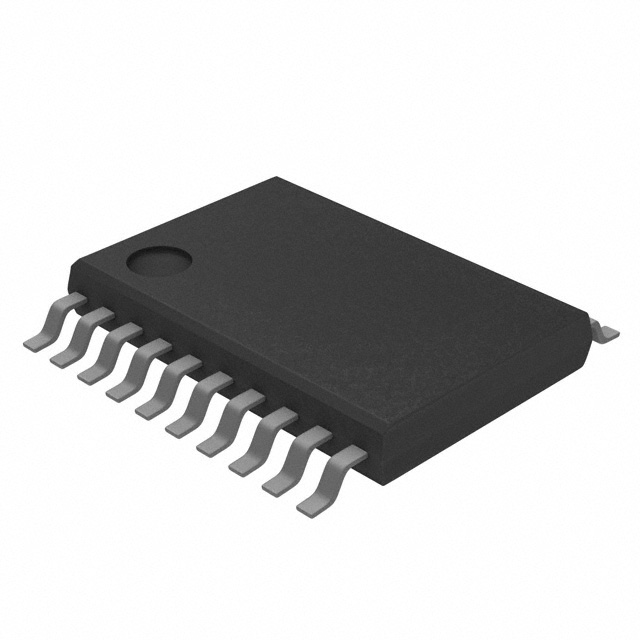
20-Pin TSSOP-PW Package
2 Applications
•
•
•
•
Appliance Display Panel
Elevator Display Panel
PLC Function Indicator
Seven-Segment Display
3 Description
The TLC6C5912 is a monolithic, medium-voltage,
low-current power 12-bit shift register designed for
use in systems that require relatively moderate load
power, such as LEDs.
This device contains a 12-bit serial-in, parallel-out
shift register that feeds a 12-bit D-type storage
register. Data transfers through both the shift and
storage registers on the rising edge of the shiftregister clock (SRCK) and the register clock (RCK),
respectively. The storage register transfers data to
the output buffer when shift register clear (CLR) is
high. A low on CLR clears all registers in the device.
Holding the output enable (G) high holds all data in
the output buffers low, and all drain outputs are off.
Holding G low makes data from the storage register
transparent to the output buffers.
This device contains a 12-bit serial-in, parallel-out
shift register that feeds a 12-bit D-type storage
register. Separate clocks are provided for both the
shift and storage registers.
Outputs are low-side, open-drain DMOS transistors
with output ratings of 40 V and 50-mA continuous
sink-current OR 200-mA PWM current with singlepulse duration less than 1 ms and average current
less than 50 mA capabilities when VCC = 5 V. The
device contains built-in thermal shutdown protection
and provides up to 2000 V of ESD protection when
tested using the human-body model and the 200-V
machine model.
The TLC6C5912 characterization is for operation over
the ambient temperature range of −40°C to 105°C.
Device Information(1)
PART NUMBER
TLC6C5912
PACKAGE
TSSOP (20)
BODY SIZE (NOM)
6.50 mm × 4.40 mm
(1) For all available packages, see the orderable addendum at
the end of the data sheet.
Typical Application Schematic
Power Supply
MCU Serial
Interface
4/3
12-Bit Shift Register
LED Driver
4/3
12-Bit Shift Register
LED Driver
Typical Cascade Topology
Power Supply
I/Os
MCU Serial
Interface
4/3
12-Bit ShiftRegister
LED Driver
3 ´ 12 LED Matrix
Typical Scan Topology
Copyright © 2016, Texas Instruments Incorporated
1
An IMPORTANT NOTICE at the end of this data sheet addresses availability, warranty, changes, use in safety-critical applications,
intellectual property matters and other important disclaimers. PRODUCTION DATA.
�TLC6C5912
SLIS180 – MAY 2016
www.ti.com
Table of Contents
1
2
3
4
5
6
7
8
Features ..................................................................
Applications ...........................................................
Description .............................................................
Revision History.....................................................
Pin Configuration and Functions .........................
Specifications.........................................................
1
1
1
2
3
4
6.1
6.2
6.3
6.4
6.5
6.6
6.7
4
4
4
5
5
5
7
Absolute Maximum Ratings ......................................
ESD Ratings..............................................................
Recommended Operating Conditions.......................
Thermal Information ..................................................
Electrical Characteristics...........................................
Switching Characteristics ..........................................
Typical Characteristics ..............................................
8.2 Functional Block Diagram ....................................... 10
8.3 Feature Description................................................. 10
8.4 Device Functional Modes........................................ 11
9
Application and Implementation ........................ 12
9.1 Application Information............................................ 12
9.2 Typical Application ................................................. 12
10 Power Supply Recommendations ..................... 15
11 Layout................................................................... 15
11.1 Layout Guidelines ................................................. 15
11.2 Layout Example .................................................... 15
12 Device and Documentation Support ................. 16
12.1
12.2
12.3
12.4
Parameter Measurement Information .................. 9
Detailed Description ............................................ 10
Community Resources..........................................
Trademarks ...........................................................
Electrostatic Discharge Caution ............................
Glossary ................................................................
16
16
16
16
13 Mechanical, Packaging, and Orderable
Information ........................................................... 16
8.1 Overview ................................................................. 10
4 Revision History
NOTE: Page numbers for previous revisions may differ from page numbers in the current version.
2
DATE
REVISION
NOTE
May 2016
*
Initial release
Submit Documentation Feedback
Copyright © 2016, Texas Instruments Incorporated
Product Folder Links: TLC6C5912
�TLC6C5912
www.ti.com
SLIS180 – MAY 2016
5 Pin Configuration and Functions
PW Package
20-Pin TSSOP
Top View
VCC
SER_IN
DRAIN0
DRAIN1
DRAIN2
DRAIN3
DRAIN4
DRAIN5
CLR
G
1
20
GND
2
3
4
19
SRCK
18
17
DRAIN11
DRAIN10
5
16
DRAIN9
6
7
15
DRAIN8
8
14
13
DRAIN7
DRAIN6
9
12
10
11
RCK
SER_OUT
Pin Functions
PIN
NAME
NO.
I/O
DESCRIPTION
Shift register clear, active-low: CLR is the signal used to clear all the registers. The
storage register transfers data to the output buffer when shift register clear CLR is high.
Driving CLR is low clears all the registers in the device.
CLR
9
I
DRAIN0
3
O
DRAIN1
4
O
DRAIN2
5
O
DRAIN3
6
O
DRAIN4
7
O
DRAIN5
8
O
DRAIN6
13
O
DRAIN7
14
O
DRAIN8
15
O
DRAIN9
16
O
DRAIN10
17
O
DRAIN11
18
O
G
10
I
Output enable, active-low: G is the LED channel enable and disable input pin. Having G
low enables all drain channels according to the output-latch register content. When high, all
channels are off.
GND
20
—
Power ground: GND is the ground reference pin for the device. This pin must connect to the
ground plane on the PCB.
RCK
12
I
Register clock: RCK is the storage register clock. The data in each shift register stage
transfers to the storage register at the rising edge of RCK. Data in the storage register
appears at the output whenever the output enable G̅ input signal is high.
SER IN
2
I
Serial-data input: SER IN is the serial data input. Data on SER IN loads into the internal
register on each rising edge of SRCK.
Open-drain output: DRAIN0 to DRAIN11 are the LED current-sink channels. These pins
connect to the LED cathodes, and they can survive up to 40-V LED supply voltage.
Submit Documentation Feedback
Copyright © 2016, Texas Instruments Incorporated
Product Folder Links: TLC6C5912
3
�TLC6C5912
SLIS180 – MAY 2016
www.ti.com
Pin Functions (continued)
PIN
NAME
NO.
I/O
DESCRIPTION
SER OUT
11
O
Serial-data output: SER OUT is the serial data output of the 12−bit serial shift register. The
purpose of this pin is to cascade several devices on the serial bus. By connecting the SER
OUT pin to the SER IN input of the next device on the serial bus to cascade, the data
transfers to the next device on the falling edge of SRCK. This can improve the cascade
application reliability, as it can avoid the issue that the second device receives SRCK and
data input at the same rising edge of SRCK.
SRCK
19
I
Shift-register clock: SRCK is the serial clock input. On each rising SRCK edge, data
transfers from SER IN to the internal serial shift registers.
VCC
1
I
Power supply: VCC is the power supply pin voltage for the device. TI recommends adding a
0.1 μF ceramic capacitor close to the pin.
6 Specifications
6.1 Absolute Maximum Ratings
over operating free-air temperature range (unless otherwise noted) (1)
MIN
VCC Logic supply voltage
VI
Logic input-voltage
–0.3
VDS Power DMOS drain-to-source voltage
Continuous total dissipation
Operating junction temperature
Tstg Storage temperature
(1)
UNIT
8
V
8
V
42
V
See Thermal Information
Operating ambient temperature (Top)
TJ
MAX
105
°C
–40
125
°C
–55
165
°C
Stresses beyond those listed under Absolute Maximum Ratings may cause permanent damage to the device. These are stress ratings
only, which do not imply functional operation of the device at these or any other conditions beyond those indicated under Recommended
Operating Conditions. Exposure to absolute-maximum-rated conditions for extended periods may affect device reliability.
6.2 ESD Ratings
VALUE
Human-body model (HBM), per ANSI/ESDA/JEDEC JS-001
V(ESD)
(1)
(2)
Electrostatic discharge
(1)
Charged-device model (CDM), per JEDEC specification JESD22C101 (2)
UNIT
±2000
V
±750
JEDEC document JEP155 states that 500-V HBM allows safe manufacturing with a standard ESD control process.
JEDEC document JEP157 states that 250-V CDM allows safe manufacturing with a standard ESD control process.
6.3 Recommended Operating Conditions
MIN
MAX
3
5.5
UNIT
VCC
Supply voltage
VIH
High-level input voltage
VIL
Low-level input voltage
tsu
Setup time, SER IN high before SRCK↑
15
ns
th
Hold time, SER IN high after SRCK↑
15
ns
tw
Pulse duration
TA
Operating ambient temperature
4
2.4
V
0.7
40
–40
Submit Documentation Feedback
V
V
ns
105
°C
Copyright © 2016, Texas Instruments Incorporated
Product Folder Links: TLC6C5912
�TLC6C5912
www.ti.com
SLIS180 – MAY 2016
6.4 Thermal Information
TLC6C5912
THERMAL METRIC (1)
PW (TSSOP)
UNIT
20 PINS
RθJA
Junction-to-ambient thermal resistance
114.8
°C/W
RθJC(top)
Junction-to-case (top) thermal resistance
44.1
°C/W
RθJB
Junction-to-board thermal resistance
61.3
°C/W
ψJT
Junction-to-top characterization parameter
4.7
°C/W
ψJB
Junction-to-board characterization parameter
60.8
°C/W
(1)
For more information about traditional and new thermal metrics, see the Semiconductor and IC Package Thermal Metrics application
report, SPRA953.
6.5 Electrical Characteristics
VCC = 5 V, TA = 25°C (unless otherwise noted)
PARAMETER
TEST CONDITIONS
MIN
TYP MAX
DRAIN0 to DRAIN11,
drain-to-source voltage
40
VOH
High-level output voltage,
SER OUT
IOH = –20 μA
VOL
Low-level output voltage,
SER OUT
IOH = 20 μA
IIH
High-level input current
VCC = 5 V, VI = VCC
IIL
Low-level input current
VCC = 5 V, VI = 0
IOH = –4 mA
IOH = 4 mA
VCC = 5 V
4.99
4.5
4.69
VCC = 5 V
0.001
0.01
0.25
0.4
μA
All outputs off
0.1
1
All outputs on
130
170
VCC = 5 V,
No clock signal
ICC(FRQ)
Logic supply current at
frequency
fSRCK = 5 MHz, CL = 30 pF, all outputs on
IDSX
Off-state drain current
300
VDS = 30 V, VCC = 5 V
ID = 20 mA, VCC = 5 V, TA = 25°C, single channel ON
0.15
0.3
6
7.4
8.6
ID = 20 mA, VCC = 5 V, TA = 25°C, all channels ON
6.7
8.9
9.6
ID = 20 mA, VCC = 3.3 V, TA = 25°C, single channel ON
7.9
9.3
11.2
Static drain-source on-state ID = 20 mA, VCC = 3.3 V, TA = 25°C, all channels ON
resistance
ID = 20 mA, VCC = 5 V, TA = 105°C, single channel ON
8.7
10.6
12.3
9.1
11.2
12.9
TSHUTDOWN
Thermal shutdown trip point
tHYS
Hysteresis
μA
µA
0.1
VDS = 30 V, TC = 125°C, VCC = 5 V
V
μA
0.2
Logic supply current
V
V
–0.2
ICC
rDS(on)
4.9
UNIT
ID = 20 mA, VCC = 5 V, TA = 105°C, all channels ON
10.3
13
14.5
ID = 20 mA, VCC = 3.3 V, TA = 105°C, single channel ON
11.6
13.7
16.4
ID = 20 mA, VCC = 3.3 V, TA = 105°C, all channels ON
12.8
15.6
18.2
150
175
200
15
μA
Ω
°C
°C
6.6 Switching Characteristics
VCC = 5 V, TA = 25°C
PARAMETER
TEST CONDITIONS
MIN
TYP MAX
UNIT
tPLH
Propagation delay time, low-to-high-level output from G
210
ns
tPHL
Propagation delay time, high-to-low-level output from G
75
ns
tr
Rise time, drain output
250
ns
tf
Fall time, drain output
200
ns
tpd
Propagation delay time, SRCK↓ to SEROUT
CL = 30 pF, ID = 48 mA
35
ns
tor
SEROUT rise time (10% to 90%)
CL = 30 pF
20
ns
tof
SEROUT fall time (90% to 10%)
CL = 30 pF
20
ns
CL = 30 pF, ID = 48 mA
Submit Documentation Feedback
Copyright © 2016, Texas Instruments Incorporated
Product Folder Links: TLC6C5912
5
�TLC6C5912
SLIS180 – MAY 2016
www.ti.com
Switching Characteristics (continued)
VCC = 5 V, TA = 25°C
PARAMETER
TEST CONDITIONS
MIN
UNIT
10
MHz
f(SRCK)
Serial clock frequency
tSRCK_WH
SRCK pulse duration, high
30
ns
tSRCK_WL
SRCK pulse duration, low
30
ns
12
11
10
CL = 30 pF, ID = 20 mA
TYP MAX
8
9
7
5
6
4
3
2
1
SRCK
SER IN
CLR
1
SER OUT
0
Figure 1. SER IN to SER OUT Waveform
Figure 1 shows the SER IN to SER OUT waveform. The output signal appears on the falling edge of the shift
register clock (SRCK) because there is a phase inverter at SER OUT (see Figure 2). As a result, it takes seven
and a half periods of SRCK for data to transfer from SER IN to SER OUT.
5V
G
50%
50%
0V
tPHL
tPLH
90%
Output
10 V
90%
10%
10%
0.5 V
tf
tr
5V
SRCK
50%
0V
tsu
th
5V
SER IN
50%
50%
0V
tw
Switching Times, Input Setup and Hold Waveforms
SRCK
50%
50%
tpd
tpd
50%
SER OUT
50%
SER OUT Propagation Delay Waveform
Figure 2. Switching Times and Voltage Waveforms
Figure 2 shows the switching times and voltage waveforms. Tests for all these parameters took place using the
test circuit shown in Figure 12.
6
Submit Documentation Feedback
Copyright © 2016, Texas Instruments Incorporated
Product Folder Links: TLC6C5912
�TLC6C5912
www.ti.com
SLIS180 – MAY 2016
6.7 Typical Characteristics
Conditions for Figure 5 and Figure 6: Single channel on; conditions for Figure 7, Figure 8, and Figure 9: All channels on.
500
700
TA = 40qC
TA = 25qC
TA = 105qC
All Channels Off
All Channels On
450
400
500
Supply Current (PA)
Supply Current (PA)
600
400
300
200
350
300
250
200
150
100
100
50
0
0
0.1
1
10
3
100
Frequency (MHz)
3.5
D001
VCC = 5 V
Figure 3. Supply Current vs Frequency
5.5
6
D002
Figure 4. Supply Current vs Supply Voltage
16
Drain-Source On-State Resistance (:)
Drain-Source On-State Resistance (:)
4.5
5
Supply Voltage (V)
VCC
14
12
10
8
6
4
TA = 40qC
TA = 25qC
TA = 105qC
2
14
12
10
8
6
4
TA = 40qC
TA = 25qC
TA = 105qC
2
0
0
0
10
20
30
40
Drain Current (mA)
50
0
60
10
D003
VCC = 5 V
20
30
40
Drain Current (mA)
50
60
D004
VCC = 3.3 V
Figure 5. Drain-to-Source On-State Resistance
vs Drain Current (Single Channel On)
Figure 6. Drain-to-Source On-State Resistance
vs Drain Current (Single Channel On)
16
20
Drain-Source On-State Resistance (:)
Drain-Source On-State Resistance (:)
4
14
12
10
8
6
4
TA = 40qC
TA = 25qC
TA = 105qC
2
0
18
16
14
12
10
8
6
4
TA = 40qC
TA = 25qC
TA = 105qC
2
0
0
10
20
30
40
Drain Current (mA)
50
60
0
10
D005
VCC = 5 V
20
30
40
Drain Current (mA)
50
60
D006
VCC = 3.3 V
Figure 7. Drain-to-Source On-State Resistance
vs Drain Current (All Channels On)
Figure 8. Drain-to-Source On-State Resistance
vs Drain Current (All Channels On)
Submit Documentation Feedback
Copyright © 2016, Texas Instruments Incorporated
Product Folder Links: TLC6C5912
7
�TLC6C5912
SLIS180 – MAY 2016
www.ti.com
Typical Characteristics (continued)
18
400
16
350
14
Switching Time (ns)
Drain-Source On-State Resistance (:)
Conditions for Figure 5 and Figure 6: Single channel on; conditions for Figure 7, Figure 8, and Figure 9: All channels on.
12
10
8
6
4
2
0
2.5
tPLH
tPHL
tr
tf
300
250
200
150
100
TA = 105qC
TA = 25qC
TA = 40qC
3
3.5
50
4
4.5
5
Supply Voltage (V)
5.5
6
6.5
0
-40
-20
D007
0
20
40
60
80
Ambient Temperature (qC)
100
120
D008
I(ds) = 20 mA
Figure 9. Drain-to-Source On-State Resistance
vs Supply Voltage
8
Figure 10. Switching Time vs Ambient Temperature
Submit Documentation Feedback
Copyright © 2016, Texas Instruments Incorporated
Product Folder Links: TLC6C5912
�TLC6C5912
www.ti.com
SLIS180 – MAY 2016
7 Parameter Measurement Information
5V
10 V
VCC
CLR
ID
RL = 200 W
SRCK
Output
MCU
DRAIN
SER IN
CL = 30 pF
(see Note A)
RCK
G
GND
Copyright © 2016, Texas Instruments Incorporated
A.
CL includes probe and jig capacitance.
Figure 11. Resistive-Load Test Circuit
12
11
10
9
8
7
6
5
4
3
2
1
SRCK
SER IN
G
RCK
0
CLR
1
DRAIN0
0
DRAIN1
0
DRAIN10
0
DRAIN11
0
Figure 12. Voltage Waveforms
Figure 11 and Figure 12 show the resistive-load test circuit and voltage waveforms. One can see from Figure 12
that with G held low and CLR held high, the status of each drain changes on the rising edge of the register clock,
indicating the transfer of data to the output buffers at that time.
Submit Documentation Feedback
Copyright © 2016, Texas Instruments Incorporated
Product Folder Links: TLC6C5912
9
�TLC6C5912
SLIS180 – MAY 2016
www.ti.com
8 Detailed Description
8.1 Overview
The TLC6C5912 device is a monolithic, medium-voltage, low current 12-bit shift register designed to drive
relatively moderate load power such LEDs. The device contains a 12-bit serial-in, parallel-out shift register that
feeds a 12-bit D-type storage register. Thermal shutdown protection is also built-into the device.
8.2 Functional Block Diagram
G
RCK
DRAIN0
CLR
D
SRCK
D
C1
CLR
C1
CLR
DRAIN1
SER IN
D
D
C1
CLR
C1
CLR
DRAIN2
D
D
C1
CLR
C1
CLR
DRAIN3
D
D
C1
CLR
C1
CLR
DRAIN4
D
D
C1
CLR
C1
CLR
DRAIN10
D
D
C1
CLR
C1
CLR
DRAIN11
D
D
C1
CLR
C1
CLR
GND
D
C1
SER OUT
CLR
8.3 Feature Description
8.3.1 Thermal Shutdown
The device implements an internal thermal shutdown to protect itself if the junction temperature exceeds 175°C
(typical). The thermal shutdown forces the device to have an open state when the junction temperature exceeds
the thermal trip threshold. Once the junction temperature decreases to less than 160°C (typical), the device
begins to operate again.
10
Submit Documentation Feedback
Copyright © 2016, Texas Instruments Incorporated
Product Folder Links: TLC6C5912
�TLC6C5912
www.ti.com
SLIS180 – MAY 2016
Feature Description (continued)
8.3.2 Serial-In Interface
The TLC6C598 device contains an 8-bit serial-in, parallel out shift register that feeds an 8-bit D-type storage
register. Data transfer through both the shift and storage registers on the rising edge of the shift register clock
(SRCK) and the register clock (RCK), respectively. The storage transfers data to the output buffer when shift
register clear (CLR) is high.
8.3.3 Clear Register
A logic low on CLR clears all registers in the device. TI suggests clearing the device during power up or
initialization.
8.3.4 Cascade Through SER OUT
By connecting the SER OUT pin to the SER IN input of the next device on the serial bus to cascade, the data
transfers to the next device on the falling edge of SRCK. This can improve the cascade application reliability, as
it can avoid that the second device receives SRCK and data input at the same rising edge of SRCK.
8.3.5 Output Control
Holding the output enable (G) high holds all data in the output buffers low, and all drain outputs are off. Holding
G low makes data from the storage register transparent to the output buffers. When data in the output buffers is
low, the DMOS transistor outputs are off. When data is high, the DMOS transistor outputs are capable of sinkcurrent. This pin also be used for global PWM dimming.
8.4 Device Functional Modes
8.4.1 Operation With VCC < 3 V
This device works normally during 3 V ≤ VCC ≤ 5.5 V, when operation voltage is lower than 3 V. The behavior of
device cannot be ensured, including communication interface and current capability.
8.4.2 Operation With 5.5 V ≤ VCC ≤ 8 V
The device works normally during this voltage range, but reliability issues may occurs while the device works for
a long time in this voltage range.
Submit Documentation Feedback
Copyright © 2016, Texas Instruments Incorporated
Product Folder Links: TLC6C5912
11
�TLC6C5912
SLIS180 – MAY 2016
www.ti.com
9 Application and Implementation
NOTE
Information in the following applications sections is not part of the TI component
specification, and TI does not warrant its accuracy or completeness. TI’s customers are
responsible for determining suitability of components for their purposes. Customers should
validate and test their design implementation to confirm system functionality.
9.1 Application Information
The TLC6C5912 device is a serial-in, parallel-out, power logic 8-bit shift register with low-side open-drain DMOS
output rating of 40 V and 50-mA continuous sink-current capabilities when VCC= 5 V. The device is designed to
drive resistive loads and is particularly well-suited as an interface between a microcontroller and LEDs or lamps.
The device also provides up to 2000 V of ESD protection when tested using the human body model and 200 V
when using the machine model.
9.2 Typical Application
Figure 13 shows a typical cascade application circuit with two TLC6C5912 chips configured to cascade topology.
The MCU generates all the input signals.
12
Submit Documentation Feedback
Copyright © 2016, Texas Instruments Incorporated
Product Folder Links: TLC6C5912
�TLC6C5912
www.ti.com
SLIS180 – MAY 2016
Typical Application (continued)
Battery 9 V–40 V
3 V–5.5 V
DRAIN0
DRAIN1
DRAIN10 DRAIN11
VCC
GND
SER IN
SRCK
MCU
G
SER OUT
CLR
RCK
DRAIN0
DRAIN1
DRAIN10 DRAIN11
VCC
SER IN
GND
SRCK
G
CLR
SER OUT
RCK
Figure 13. Typical Application Circuit
9.2.1 Design Requirements
Table 1 lists the parameters for this design example.
Table 1. Design Parameters
DESIGN PARAMETER
EXAMPLE VALUE
Vbattery
9 V to 40 V
VCC _ 1
3.3 V
I(D0), I(D1), I(D2), I(D3) , I(D4), I(D5), I(D6), I(D7), I(D8), I(D9), I(D10), I(D11)
30 mA
VCC _ 2
5V
I(D12), I(D13), I(D14), I(D15) , I(D16), I(D17), I(D18), I(D19), I(D20), I(D21), I(D122),
I(D23)
50 mA
Submit Documentation Feedback
Copyright © 2016, Texas Instruments Incorporated
Product Folder Links: TLC6C5912
13
�TLC6C5912
SLIS180 – MAY 2016
www.ti.com
9.2.2 Detailed Design Procedure
To
•
•
•
begin the design process, the designer must decide on a few parameters:
Vsupply: LED supply voltage
VDx: LED forward voltage
I: LED current
After determining the parameters, calculate the resistor in series with LED using Equation 1.
Rx = (Vsupply – VDx) / I
(1)
9.2.3 Application Curve
Figure 14. TLC6C5912 Application Waveform
14
Submit Documentation Feedback
Copyright © 2016, Texas Instruments Incorporated
Product Folder Links: TLC6C5912
�TLC6C5912
www.ti.com
SLIS180 – MAY 2016
10 Power Supply Recommendations
The TLC6C5912 device is designed to operate from an input voltage supply range from 3 V to 5.5 V. This input
supply should be well regulated. TI recommends placing the ceramic bypass capacitors near the VCC pin.
11 Layout
11.1 Layout Guidelines
There are no special layout requirement for the digital signal pins. The only requirement is placing the ceramic
bypass capacitors near the corresponding pin.
Maximize the copper coverage on the PCB to increase the thermal conductivity of the board. The major heat-flow
path from the package to the ambient is through the cooper on the PCB. Maximizing the copper coverage is
extremely important when the design does not include heat sinks attached to the PCB on the other side of the
package.
• Add as many thermal vias as possible directly under the package ground pad to optimize the thermal
conductivity of the board.
• All thermal vias should be either plated shut or plugged and capped on both sides of the board to prevent
solder voids. To ensure reliability and performance, the solder coverage should be at least 85%.
11.2 Layout Example
Vcc
1
20
GND
SER IN
2
19
SRCK
DRAIN0
3
18
DRAIN11
DRAIN1
4
17
DRAIN10
DRAIN2
5
16
DRAIN9
DRAIN3
6
15
DRAIN8
DRAIN4
7
14
DRAIN7
DRAIN5
8
13
DRAIN6
CLR
9
12
RCK
G
10
11
SER OUT
Figure 15. Layout Recommendation
Submit Documentation Feedback
Copyright © 2016, Texas Instruments Incorporated
Product Folder Links: TLC6C5912
15
�TLC6C5912
SLIS180 – MAY 2016
www.ti.com
12 Device and Documentation Support
12.1 Community Resources
The following links connect to TI community resources. Linked contents are provided "AS IS" by the respective
contributors. They do not constitute TI specifications and do not necessarily reflect TI's views; see TI's Terms of
Use.
TI E2E™ Online Community TI's Engineer-to-Engineer (E2E) Community. Created to foster collaboration
among engineers. At e2e.ti.com, you can ask questions, share knowledge, explore ideas and help
solve problems with fellow engineers.
Design Support TI's Design Support Quickly find helpful E2E forums along with design support tools and
contact information for technical support.
12.2 Trademarks
E2E is a trademark of Texas Instruments.
All other trademarks are the property of their respective owners.
12.3 Electrostatic Discharge Caution
These devices have limited built-in ESD protection. The leads should be shorted together or the device placed in conductive foam
during storage or handling to prevent electrostatic damage to the MOS gates.
12.4 Glossary
SLYZ022 — TI Glossary.
This glossary lists and explains terms, acronyms, and definitions.
13 Mechanical, Packaging, and Orderable Information
The following pages include mechanical, packaging, and orderable information. This information is the mostcurrent data available for the designated device. This data is subject to change without notice and without
revision of this document. For browser-based versions of this data sheet, see the left-hand navigation pane.
16
Submit Documentation Feedback
Copyright © 2016, Texas Instruments Incorporated
Product Folder Links: TLC6C5912
�PACKAGE OPTION ADDENDUM
www.ti.com
10-Dec-2020
PACKAGING INFORMATION
Orderable Device
Status
(1)
Package Type Package Pins Package
Drawing
Qty
Eco Plan
(2)
Lead finish/
Ball material
MSL Peak Temp
Op Temp (°C)
Device Marking
(3)
(4/5)
(6)
TLC6C5912PWR
ACTIVE
TSSOP
PW
20
2000
RoHS & Green
NIPDAU
Level-3-260C-168 HR
-40 to 105
6C5912I
(1)
The marketing status values are defined as follows:
ACTIVE: Product device recommended for new designs.
LIFEBUY: TI has announced that the device will be discontinued, and a lifetime-buy period is in effect.
NRND: Not recommended for new designs. Device is in production to support existing customers, but TI does not recommend using this part in a new design.
PREVIEW: Device has been announced but is not in production. Samples may or may not be available.
OBSOLETE: TI has discontinued the production of the device.
(2)
RoHS: TI defines "RoHS" to mean semiconductor products that are compliant with the current EU RoHS requirements for all 10 RoHS substances, including the requirement that RoHS substance
do not exceed 0.1% by weight in homogeneous materials. Where designed to be soldered at high temperatures, "RoHS" products are suitable for use in specified lead-free processes. TI may
reference these types of products as "Pb-Free".
RoHS Exempt: TI defines "RoHS Exempt" to mean products that contain lead but are compliant with EU RoHS pursuant to a specific EU RoHS exemption.
Green: TI defines "Green" to mean the content of Chlorine (Cl) and Bromine (Br) based flame retardants meet JS709B low halogen requirements of