�������
� �
���
� �� ���� �
���
�
��
SLOS065D − MARCH 1991 − REVISED APRIL 2002
D 2.5-V Virtual Ground for 5-V/GND Analog
D
D
D Excellent Regulation Characteristics
Systems
High Output-Current Capability
Sink or Source . . . 20 mA Typ
Micropower Operation . . . 170 µA Typ
− Output Regulation
−45 µV Typ at IO = 0 to −10 mA
+15 µV Typ at IO = 0 to + 10 mA
− Input Regulation = 1.5 µV/V Typ
Low-Impedance Output . . . 0.0075 Ω Typ
Macromodel Included
D
D
description
OUTPUT REGULATION
100
In signal-conditioning applications using a single
power source, a reference voltage is required for
termination of all signal grounds. To accomplish
this, engineers have typically used solutions
consisting of resistors, capacitors, operational
amplifiers, and voltage references. Texas Instruments has eliminated all of those components
with one easy-to-use 3-terminal device. That
device is the TLE2425 precision virtual ground.
VI = 5 V
∆VV)
O − Output Voltage Change − µV
80
Use of the TLE2425 over other typical circuit
solutions gives the designer increased dynamic
signal range, improved signal-to-noise ratio,
lower distortion, improved signal accuracy, and
easier interfacing to ADCs and DACs. These
benefits are the result of combining a precision
micropower voltage reference and a high-performance precision operational amplifier in a single
silicon chip. It is the precision and performance of
these two circuit functions together that yield such
dramatic system-level performance.
60
TA = − 40°C
40
TA = 0°C
TA = − 55°C
20
0
TA = 125°C
TA = 25°C
TA = 25°C
−20
−40
TA = 125°C
−60
TA = − 55°C
−80
−100
−10
−8
−6
−4 −2
0
2
4
6
IO − Output Current − mA
8
10
The TLE2425 improves input regulation as well as output regulation and, in addition, reduces output impedance
and power dissipation in a majority of virtual-ground-generation circuits. Both input regulation and load
regulation exceed 12 bits of accuracy on a single 5-V system. Signal-conditioning front ends of data acquisition
systems that push 12 bits and beyond can use the TLE2425 to eliminate a major source of system error.
AVAILABLE OPTIONS
TA
SMALL OUTLINE
(D)
PLASTIC
TO-226AA
(LP)
0°C to 70°C
TLE2425CD
TLE2425CD
−40°C to 85°C
TLE2425ID
TLE2425ID
−55°C to 125°C
TLE2425MD
—
† The D package is available taped and reeled. Add R suffix to
the device type (e.g., TLE2425CDR).
Please be aware that an important notice concerning availability, standard warranty, and use in critical applications of
Texas Instruments semiconductor products and disclaimers thereto appears at the end of this data sheet.
Copyright 2002, Texas Instruments Incorporated
�
��
��
� ���� ����������� �� ������� �� �� !�"#������� $���%
���$���� ������� �� �!������������ !�� �&� ����� �� ��'�� �����������
����$��$ (������)% ���$������ !��������* $��� ��� ���������#) ���#�$�
������* �� �## !���������%
WWW.TI.COM
POST OFFICE BOX 1443 HOUSTON, TEXAS 77251−1443
•
1
��������
� �
���
� �� ���� �
���
�
�
SLOS065D − MARCH 1991 − REVISED APRIL 2002
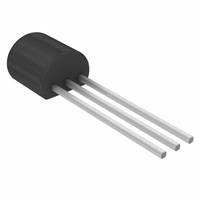
D, OR JG PACKAGE
(TOP VIEW)
OUT
COMMON
IN
NC
1
8
2
7
3
6
4
5
LP PACKAGE
(TOP VIEW)
NC
NC
NC
NC
IN
COMMON
OUT
NC − No internal connection
absolute maximum ratings over operating free-air temperature range (unless otherwise noted)†
Continuous input voltage, VI . . . . . . . . . . . . . . . . . . . . . . . . . . . . . . . . . . . . . . . . . . . . . . . . . . . . . . . . . . . . . . . . . 40 V
Output current, IO . . . . . . . . . . . . . . . . . . . . . . . . . . . . . . . . . . . . . . . . . . . . . . . . . . . . . . . . . . . . . . . . . . . . . . . ±80 mA
Duration of short-circuit current at (or below) 25°C (see Note 1) . . . . . . . . . . . . . . . . . . . . . . . . . . . . . . unlimited
Continuous total power dissipation . . . . . . . . . . . . . . . . . . . . . . . . . . . . . . . . . . . . . See Dissipation Rating Table
Operating free-air temperature range, TA: C-suffix . . . . . . . . . . . . . . . . . . . . . . . . . . . . . . . . . . . . . . 0°C to 70°C
I-suffix . . . . . . . . . . . . . . . . . . . . . . . . . . . . . . . . . . . . −40°C to 85°C
M-suffix . . . . . . . . . . . . . . . . . . . . . . . . . . . . . . . . . . −55°C to 125°C
Storage temperature range, Tstg . . . . . . . . . . . . . . . . . . . . . . . . . . . . . . . . . . . . . . . . . . . . . . . . . . . −65°C to 150°C
Lead temperature 1,6 mm (1/16 inch) from case for 10 seconds: D package . . . . . . . . . . . . . . . . . . . . . 260°C
Lead temperature 1,6 mm (1/16 inch) from case for 60 seconds: JG or LP package . . . . . . . . . . . . . . 300°C
† Stresses beyond those listed under “absolute maximum ratings” may cause permanent damage to the device. These are stress ratings only, and
functional operation of the device at these or any other conditions beyond those indicated under “recommended operating conditions” is not
implied. Exposure to absolute-maximum-rated conditions for extended periods may affect device reliability.
NOTE 1: The output may be shorted to either supply. Temperature and/or supply voltages must be limited to ensure that the maximum dissipation
rating is not exceeded.
DISSIPATION RATING TABLE
PACKAGE
TA ≤ 25
25°C
C
POWER RATING
DERATING FACTOR
ABOVE TA = 25°C
TA = 70
70°C
C
POWER RATING
TA = 85
85°C
C
POWER RATING
TA = 125
125°C
C
POWER RATING
D
725 mV
5.8 mW/°C
464 mW
377 mW
145 mW
JG
1050 mV
8.4 mW/°C
672 mW
546 mW
210 mW
LP
775 mV
6.2 mW/°C
496 mW
403 mW
155 mW
recommended operating conditions
C-SUFFIX
I-SUFFIX
M-SUFFIX
MIN
MAX
MIN
MAX
MIN
Input voltage, VI
4
40
4
40
4
40
V
Operating free-air temperature, TA
0
70
−40
85
−55
125
°C
2
WWW.TI.COM
POST OFFICE BOX 1443 HOUSTON, TEXAS 77251−1443
•
MAX
UNIT
��������
� �
���
� �� ���� �
���
�
�
SLOS065D − MARCH 1991 − REVISED APRIL 2002
electrical characteristics at specified free-air temperature, VI = 5 V, IO = 0 (unless otherwise noted)
PARAMETER
Output voltage
MIN
TYP
MAX
25°C
2.48
2.5
2.52
Full range
2.47
Temperature coefficient of output voltage
Bias current
IO = 0
TLE2425C
TA†
TEST CONDITIONS
25°C
20
25°C
170
Full range
VI = 4.5 V to 5.5 V
Full range
VI = 4 V to 40 V
Full range
Input voltage regulation
1.5
∆VI(PP) = 1 V
f = 120 Hz,
Output voltage regulation (source current)‡
1.5
25
25°C
80
Full range
−250
IO = 0 to − 20 mA
25°C
−450
−150
450
25°C
−160
15
160
Full range
−250
25°C
−235
Noncumulative
25°C
Short-circuit output current (source current)
Output noise voltage, rms
f = 10 Hz to 10 kHz
25°C
25°C
VO to 0.1%,
IO = ± 10 mA
CL = 0
VO to 0.01%,
IO = ± 10 mA
CL = 0
Output voltage response to input voltage step
VI = 4.5 to 5.5 V,
VI = 4.5 to 5.5 V,
VO to 0.1%
VO to 0.01%
25°C
Output voltage turn-on response
VI = 0 to 5 V,
VI = 0 to 5 V,
VO to 0.1%
VO to 0.01%
25°C
Output voltage response to output current step
CL = 100 pF
250
250
65
7.5
30
55
−30
−50
100
µV
V
µV/V
V/V
160
µV
µV
235
15
25°C
VO = 5 V
VO = 0
−45
µA
A
dB
IO = 0 to − 10 mA
Output impedance
Short-circuit output current (sink current)
20
−160
IO = 0 to 20 mA
∆t = 1000 h,
Long-term drift of output voltage
20
25°C
IO = 0 to 10 mA
Output voltage regulation (sink current)‡
250
25
25°C
V
ppm/°C
250
25°C
Ripple rejection
2.53
UNIT
ppm
22.5
mΩ
mA
µV
110
115
25°C
CL = 100 pF
180
µss
180
12
30
125
210
µss
µss
† Full range is 0°C to 70°C.
‡ The listed values are not production tested.
WWW.TI.COM
POST OFFICE BOX 1443 HOUSTON, TEXAS 77251−1443
•
3
��������
� �
���
� �� ���� �
���
�
�
SLOS065D − MARCH 1991 − REVISED APRIL 2002
electrical characteristics at specified free-air temperature, VI = 5 V, IO = 0 (unless otherwise noted)
PARAMETER
TEST CONDITIONS
Output voltage
Temperature coefficient of output voltage
Bias current
IO = 0
TLE2425I
TA†
MIN
TYP
MAX
25°C
2.48
2.5
2.52
Full range
2.47
25°C
20
25°C
170
Full range
VI = 4.5 V to 5.5 V
Full range
VI = 4 V to 40 V
Full range
Input voltage regulation
∆VI(PP) = 1 V
f = 120 Hz,
1.5
75
25°C
80
Full range
−250
IO = 0 to − 20 mA
25°C
−450
−150
450
25°C
−160
15
160
Full range
−250
25°C
−235
Noncumulative
25°C
Short-circuit output current (source current)
Output noise voltage, rms
f = 10 Hz to 10 kHz
25°C
25°C
VO to 0.1%,
IO = ± 10 mA
CL = 0
VO to 0.01%,
IO = ± 10 mA
CL = 0
Output voltage response to input voltage step
VI = 4.5 to 5.5 V,
VI = 4.5 to 5.5 V,
VO to 0.1%
VO to 0.01%
25°C
Output voltage turn-on response
VI = 0 to 5 V,
VI = 0 to 5 V,
VO to 0.1%
VO to 0.01%
25°C
Output voltage response to output current step
CL = 100 pF
WWW.TI.COM
POST OFFICE BOX 1443 HOUSTON, TEXAS 77251−1443
•
250
7.5
30
55
−30
−50
100
µV/V
V/V
µV
µV
235
ppm
22.5
mΩ
mA
µV
110
115
25°C
CL = 100 pF
† Full range is − 40°C to 85°C.
‡ The listed values are not production tested.
250
65
µV
V
160
15
25°C
VO = 5 V
VO = 0
−45
µA
A
dB
IO = 0 to − 10 mA
Output impedance
Short-circuit output current (sink current)
20
−160
IO = 0 to 20 mA
∆t = 1000 h,
Long-term drift of output voltage
20
25°C
IO = 0 to 8 mA
Output voltage regulation (sink current)‡
250
75
25°C
Output voltage regulation (source current)‡
4
1.5
V
ppm/°C
250
25°C
Ripple rejection
2.53
UNIT
180
µss
180
12
30
125
210
µss
µss
��������
� �
���
� �� ���� �
���
�
�
SLOS065D − MARCH 1991 − REVISED APRIL 2002
electrical characteristics at specified free-air temperature, VI = 5 V, IO = 0 (unless otherwise noted)
PARAMETER
Output voltage
MIN
TYP
MAX
25°C
2.48
2.5
2.52
Full range
2.47
Temperature coefficient of output voltage
Bias current
IO = 0
TLE2425M
TA†
TEST CONDITIONS
25°C
20
25°C
170
Full range
VI = 4.5 V to 5.5 V
Full range
VI = 4.5 V to 40 V
Full range
Input voltage regulation
1.5
∆VI(PP) = 1 V
f = 120 Hz,
Output voltage regulation (source current)‡
1.5
25°C
80
Full range
−250
IO = 0 to − 20 mA
25°C
−450
−150
450
25°C
−160
15
160
Full range
−250
25°C
−235
Noncumulative
25°C
Short-circuit output current (source current)
Output noise voltage, rms
f = 10 Hz to 10 kHz
25°C
25°C
VO to 0.1%,
IO = ± 10 mA
CL = 0
VO to 0.01%,
IO = ± 10 mA
CL = 0
Output voltage response to input voltage step
VI = 4.5 to 5.5 V,
VI = 4.5 to 5.5 V,
VO to 0.1%
VO to 0.01%
25°C
Output voltage turn-on response
VI = 0 to 5 V,
VI = 0 to 5 V,
VO to 0.1%
VO to 0.01%
25°C
Output voltage response to output current step
CL = 100 pF
250
250
65
7.5
30
55
−30
−50
100
µV
V
µV/V
V/V
160
µV
µV
235
15
25°C
VO = 5 V
VO = 0
−45
µA
A
dB
IO = 0 to − 10 mA
Output impedance
Short-circuit output current (sink current)
20
100
−160
IO = 0 to 20 mA
∆t = 1000 h,
Long-term drift of output voltage
20
25°C
IO = 0 to 3 mA
Output voltage regulation (sink current)‡
250
100
25°C
V
ppm/°C
250
25°C
Ripple rejection
2.53
UNIT
ppm
22.5
mΩ
mA
µV
110
115
25°C
CL = 100 pF
180
µss
180
12
30
125
210
µss
µs
† Full range is − 55°C to 125°C.
‡ The listed values are not production tested.
WWW.TI.COM
POST OFFICE BOX 1443 HOUSTON, TEXAS 77251−1443
•
5
��������
� �
���
� �� ���� �
���
�
�
SLOS065D − MARCH 1991 − REVISED APRIL 2002
TYPICAL CHARACTERISTICS
Table Of Graphs
FIGURE
Output voltage
Output voltage hysteresis
Input bias current
Distribution
1
vs Free-air temperature
2
vs Free-air temperature
3
vs Input voltage
4
vs Free-air temperature
5
Input voltage regulation
6
Ripple rejection
vs Frequency
Output voltage regulation
6
7
8
Output impedance
vs Frequency
9
Short-circuit output current
vs Free-air temperature
10
Spectral noise voltage density
vs Frequency
11
Wide-band noise voltage
vs Frequency
12
Output voltage change with current step
vs Time
13
Output voltage change with voltage step
vs Time
14
Output voltage power-up response
vs Time
15
Output current
vs Load capacitance
16
WWW.TI.COM
POST OFFICE BOX 1443 HOUSTON, TEXAS 77251−1443
•
��������
� �
���
� �� ���� �
���
�
�
SLOS065D − MARCH 1991 − REVISED APRIL 2002
TYPICAL CHARACTERISTICS†
OUTPUT VOLTAGE
vs
FREE-AIR TEMPERATURE
DISTRIBUTION OF
OUTPUT VOLTAGE
24
VI = 5 V
TA = 25°C
2.53
100 Units Tested
From 1 Wafer Lot
VI = 5 V
IO = 0
2.52
VV)
O − Output Voltage − V
Percentage of Units − %
20
16
12
8
4
2.51
2.5
2.49
2.48
0
2.48
2.5
2.49
2.51
2.47
−75
2.52
−50
VO − Output Voltage − V
−25
Figure 1
50
75
100
125
35
40
INPUT BIAS CURRENT
vs
INPUT VOLTAGE
4
250
VI = 5 V
Normalized to First 25°C VO
IO = 0
TA = 25°C
IIB
I IB − Input Bias Current − µ A
Output Voltage Hysteresis − mV
25
Figure 2
OUTPUT VOLTAGE HYSTERESIS
vs
FREE-AIR TEMPERATURE
2
0
TA − Free-Air Temperature − °C
Start Point
0
End Point
−2
−4
−6
200
150
100
50
−8
−10
−75
0
−50
−25
0
25
50
75
100
125
0
5
10
TA − Free-Air Temperature − °C
Figure 3
25
15
20
30
VI − Input Voltage − V
Figure 4
† Data at high and low temperatures are applicable within rated operating free-air temperature ranges of the various devices.
WWW.TI.COM
POST OFFICE BOX 1443 HOUSTON, TEXAS 77251−1443
•
7
��������
� �
���
� �� ���� �
���
�
�
SLOS065D − MARCH 1991 − REVISED APRIL 2002
TYPICAL CHARACTERISTICS†
INPUT BIAS CURRENT
vs
FREE-AIR TEMPERATURE
172
INPUT VOLTAGE REGULATION
80
VI = 5 V
IO = 0
170
IO = 0
TA = 25°C
∆ VV)
O − Output Voltage Change − µV
IIB
I IB − Input Bias Current − µ A
168
166
164
162
160
158
156
154
60
40
20
0
152
150
−75 −50
−20
−25
0
25
50
75
100
TA − Free-Air Temperature − °C
125
0
Figure 5
OUTPUT VOLTAGE REGULATION
100
90
VI = 5 V
80
∆VV)
O − Output Voltage Change − µV
80
70
60
50
40
30
VI = 5 V
∆VI(PP) = 1 V
IO = 0
TA = 25°C
20
10
10
100
60
TA = − 40°C
TA = 0°C
40
TA = − 55°C
20
0
−20
−40
10 k
100 k
1M
TA = 125°C
−60
−80
1k
TA = 125°C
TA = 25°C
TA = 25°C
−100
−10 −8
f − Frequency − Hz
Figure 7
TA = − 55°C
−6
−4 −2
0
2
4
6
IO − Output Current − mA
Figure 8
† Data at high and low temperatures are applicable within rated operating free-air temperature ranges of the various devices.
8
40
Figure 6
RIPPLE REJECTION
vs
FREQUENCY
Ripple Rejection − dB
30
10
20
VI − Input Voltage − V
WWW.TI.COM
POST OFFICE BOX 1443 HOUSTON, TEXAS 77251−1443
•
8
10
��������
� �
���
� �� ���� �
���
�
�
SLOS065D − MARCH 1991 − REVISED APRIL 2002
TYPICAL CHARACTERISTICS
OUTPUT IMPEDANCE
vs
FREQUENCY
SHORT-CIRCUIT OUTPUT CURRENT
vs
FREE-AIR TEMPERATURE
56
100
IO = 0
IOS
I OS − Short-Circuit Output Current − mA
VI = 5 V
TA = 25°C
z o − Output Impedance − Ω
10
IO = 10 mA
1
0.1
IO = − 10 mA
0.01
10
100
1k
10 k
100 k
1M
−IOS
Output Source, VO = 0
52
50
48
46
44
42
40
0.001
IOS
Output Sink, VO = 5 V
54
VI = 5 V
−75 −50
f − Frequency − Hz
75 100
0
25
50
−25
TA − Free-Air Temperature − °C
Figure 9
Figure 10
WIDE-BAND NOISE VOLTAGE
vs
FREQUENCY
1400
80
1200
70
Wide-Band Noise Voltage − µV
V rms
Vn − Spectral Noise Voltage Density − nV/ Hz
SPECTRAL NOISE VOLTAGE DENSITY
vs
FREQUENCY
1000
800
600
400
200
VI = 5 V
TA = 25°C
0
1
10
125
100
1k
f − Frequency − Hz
10 k
100 k
VI = 5 V
TA = 25°C
1 Hz to Frequency Indicated
60
1 Pole Low Pass
50
40
30
20
2 Pole Low Pass
10
0
10
100
1k
10 k
100 k
f − Frequency − Hz
Figure 11
Figure 12
WWW.TI.COM
POST OFFICE BOX 1443 HOUSTON, TEXAS 77251−1443
•
9
��������
� �
���
� �� ���� �
���
�
�
SLOS065D − MARCH 1991 − REVISED APRIL 2002
TYPICAL CHARACTERISTICS
OUTPUT VOLTAGE RESPONSE
TO INPUT VOLTAGE STEP
vs
TIME
OUTPUT VOLTAGE RESPONSE
TO OUTPUT CURRENT STEP
vs
TIME
500
4
4
VI = 5 V
CL = 100 pF
TA = 25°C
3
0.1 %
2
1
∆V O − Change In Output Voltage − mV
∆V O − Change In Output Voltage − mV
1.5 V
0.01 %
0
VO Response
0.01 %
−1
−2
10 mA
−3
IO Step
0.1 %
0
−10 mA
−4
150
300
450
600
750
t − Time − �s
900
IO = 0
CL = 100 pF
TA = 25°C
1050
0.1 %
2
1
0
0.01 %
VO Response
−1
VI = 5.5 V
−2
0.1 %
−3
VI = 4.5 V
−4
VI Step
−500
0
−1.5 V
0
3
50
Figure 13
VI = 4.5 V
100
t − Time � �s
200
150
Figure 14
STABILITY RANGE
OUTPUT VOLTAGE POWER-UP RESPONSE
vs
TIME
3
OUTPUT CURRENT
vs
LOAD CAPACITANCE
20
IO = 0
CL = 100 pF
TA = 25°C
0.1 %
15
Unstable
10
I O − Output Current − mA
VV)
O − Output Voltage − V
2
VI = 5 V
TA = 25°C
Output Voltage Response
1
0
5
5
0
−5
Stable
−10
−15
Input Voltage Step
0
0
10
t − Time � �s
20
130
−20
10 −6 10 −5 10 −4 10 −3 10 −2 10 −1 10 0
CL− Load Capacitance − �F
Figure 15
10
Figure 16
WWW.TI.COM
POST OFFICE BOX 1443 HOUSTON, TEXAS 77251−1443
•
10 1
10 2
��������
� �
���
� �� ���� �
���
�
�
SLOS065D − MARCH 1991 − REVISED APRIL 2002
macromodel information
* TLE2425 OPERATIONAL AMPLIFIER “MACROMODEL” SUBCIRCUIT
* CREATED USING PARTS RELEASE 4.03 ON 08/21/90 AT 13:51
* REV (N/A)
SUPPLY VOLTAGE: 5 V
* CONNECTIONS: INPUT
*
| COMMON
*
| | OUTPUT
*
| | |
.SUBCKT TLE2425 3 4 5
*
*
+
OPAMP
C1
C2
C3
CPSR
DCM+
DCM−
DC
DE
DLN
DLP
DP
ECMR
EGND
EPSR
ENSE
FB
−10E6
GA
GCM
GPSR
GRC1
GRC2
GRE1
GRE2
HLIM
HCMR
IRP
IEE
IIO
I1
Q1
Q2
R2
RCM
REE
RN1
RN2
SECTION
11 12 21.66E − 12
6 7 30.00E − 12
87 0 10.64E − 9
85 86 15.9E − 9
81 82 DX
83 81 DX
5 53 DX
54 5 DX
92 90 DX
90 91 DX
4 3 DX
84 99 (2,99) 1
99 0 POLY(2)
(3,0) (4,0) 0 .5 .5
85 0 POLY(1)
(3,4) −16.22E−6 3.24E−6
89 2 POLY(1)
(88,0) 120E−6 1
7 99 POLY(6)
VB VC VE VLP VLN VPSR
O
74E6
6 0 11 12 320.4E−6
0 6 10 99 1.013E−9
85 86 (85,86)
100E−6
4 11 (4,11) 3.204E−4
4 12 (4,12) 3.204E−4
13 10 (13,10)
1.038E−3
14 10 (14,10)
1.038E−3
90 0 VLIM
1K
80 1 POLY(2)
VCM+
VCM−
0 1E2 1E2
3 4 146E−6
3 10 DC 24.05E−6
2 0 .2E−9
88 0 1E−21
11 89 13 QX
12 80 14 QX
6 9 100.0E3
84 81 1K
10 99 8.316E6
87 0 2.55E8
87 88 11.67E3
74.8E6 −10E6 10E6
WWW.TI.COM
POST OFFICE BOX 1443 HOUSTON, TEXAS 77251−1443
•
10E6
11
��������
� �
���
� �� ���� �
���
�
�
SLOS065D − MARCH 1991 − REVISED APRIL 2002
macromodel information (continued)
RO1
8 5 63
RO2
7 99 62
VCM+
82 99 1.0
VCM−
83 99 −2.3
VB
9 0 DC 0
VC
3 53 DC 1.400
VE
54 4 DC 1.400
VLIM
7 8 DC 0
VLP
91 0 DC 30
VLN
0 92 DC 30
VPSR
0 86 DC 0
RFB
5 2 1K
RIN
30 1 1K
RCOM
34 4 .1
*REGULATOR SECTION
RG1
30 0 20MEG
RG2
30 31 .2
RG3
31 35 400K
RG4
35 34 411K
RG5
31 36 25MEG
HREG
31 32 POLY(2)
VPSET VNSET 0 1E2 1E2
VREG
32 33 DC 0V
EREG
33 34 POLY(1)
(36,34)
1.23 1
VADJ
36 34 1.27V
HPSET 37 0 VREG
1.030E3
VPSET 38 0 DC 20V
HNSET 39 0 VREG
6.11E5
VNSET 40 0 DC −20V
DSUB
4 34 DX
DPOS
37 38 DX
DNNEG 40 39 DX
.MODEL DX D(IS=800.0E−18)
.MODEL QX PNP(IS=800.0E−18 BF=480)
.ENDS
12
WWW.TI.COM
POST OFFICE BOX 1443 HOUSTON, TEXAS 77251−1443
•
�PACKAGE OPTION ADDENDUM
www.ti.com
14-Oct-2022
PACKAGING INFORMATION
Orderable Device
Status
(1)
Package Type Package Pins Package
Drawing
Qty
Eco Plan
(2)
Lead finish/
Ball material
MSL Peak Temp
Op Temp (°C)
Device Marking
(3)
Samples
(4/5)
(6)
TLE2425CD
ACTIVE
SOIC
D
8
75
RoHS & Green
NIPDAU
Level-1-260C-UNLIM
2425C
Samples
TLE2425CDR
ACTIVE
SOIC
D
8
2500
RoHS & Green
NIPDAU
Level-1-260C-UNLIM
2425C
Samples
TLE2425CLP
ACTIVE
TO-92
LP
3
1000
RoHS & Green
SN
N / A for Pkg Type
2425C
Samples
TLE2425CPS
ACTIVE
SO
PS
8
80
RoHS & Green
NIPDAU
Level-1-260C-UNLIM
Q2425
Samples
TLE2425CPSR
ACTIVE
SO
PS
8
2000
RoHS & Green
NIPDAU
Level-1-260C-UNLIM
Q2425
Samples
TLE2425ID
ACTIVE
SOIC
D
8
75
RoHS & Green
NIPDAU
Level-1-260C-UNLIM
2425I
Samples
TLE2425IDG4
ACTIVE
SOIC
D
8
75
RoHS & Green
NIPDAU
Level-1-260C-UNLIM
2425I
Samples
TLE2425IDR
ACTIVE
SOIC
D
8
2500
RoHS & Green
NIPDAU
Level-1-260C-UNLIM
2425I
Samples
TLE2425ILP
ACTIVE
TO-92
LP
3
1000
RoHS & Green
SN
N / A for Pkg Type
2425I
Samples
TLE2425MD
ACTIVE
SOIC
D
8
75
RoHS & Green
NIPDAU
Level-1-260C-UNLIM
-55 to 125
2425M
Samples
TLE2425MDRG4
ACTIVE
SOIC
D
8
2500
RoHS & Green
NIPDAU
Level-1-260C-UNLIM
-55 to 125
2425M
Samples
(1)
The marketing status values are defined as follows:
ACTIVE: Product device recommended for new designs.
LIFEBUY: TI has announced that the device will be discontinued, and a lifetime-buy period is in effect.
NRND: Not recommended for new designs. Device is in production to support existing customers, but TI does not recommend using this part in a new design.
PREVIEW: Device has been announced but is not in production. Samples may or may not be available.
OBSOLETE: TI has discontinued the production of the device.
(2)
RoHS: TI defines "RoHS" to mean semiconductor products that are compliant with the current EU RoHS requirements for all 10 RoHS substances, including the requirement that RoHS substance
do not exceed 0.1% by weight in homogeneous materials. Where designed to be soldered at high temperatures, "RoHS" products are suitable for use in specified lead-free processes. TI may
reference these types of products as "Pb-Free".
RoHS Exempt: TI defines "RoHS Exempt" to mean products that contain lead but are compliant with EU RoHS pursuant to a specific EU RoHS exemption.
Green: TI defines "Green" to mean the content of Chlorine (Cl) and Bromine (Br) based flame retardants meet JS709B low halogen requirements of