Order
Now
Product
Folder
Support &
Community
Tools &
Software
Technical
Documents
TLIN1441-Q1
SLLSF27C – NOVEMBER 2018 – REVISED MAY 2020
TLIN1441-Q1 Automotive Local Interconnect Network (LIN) Transceiver with Integrated
Voltage Regulator and Watchdog
1 Features
2 Applications
•
•
•
•
•
1
•
•
•
•
•
•
•
AEC-Q100: Qualified for automotive applications
– Temperature grade 1: –40°C To 125°C TA
Local interconnect network (LIN) physical layer
specification ISO/DIS 17987–4.2 compliant and
conforms to SAE J2602 recommended practice
for LIN (See SLLA494)
Supports 12-V applications
Integrated watchdog supervisor configurable by
pin or serial peripheral interface SPI
Wide operating ranges
– 5.5 V to 28 V supply voltage
– ±42 V LIN bus fault protection
– LDO output supporting 3.3 V (TLIN14413-Q1)
or 5 V (TLIN14415-Q1)
– Sleep mode: ultra-low current
consumption allows wake up event from:
– LIN bus
– Local wake up through EN
– Local wake up through WAKE
– Power up and down glitch-free operation
Protection features:
– ESD protection
– Under-voltage protection on VSUP
– TXD dominant time out (DTO) protection
– Thermal-shutdown protection
– Unpowered node or ground disconnection failsafe at system level
VCC sources 125 mA with 12 VSUP at 100°C
Available in Leadless VSON (14) package with
improved automated optical inspection (AOI)
capability
Simplified Schematics, SPI Mode
VBAT
VSUP
Body electronics and lighting
Hybrid, electric & powertrain systems
Automotive infotainment and cluster
Appliances
3 Description
The TLIN1441-Q1 is a local interconnect network
(LIN) physical layer transceiver, compliant to LIN 2.2A
and ISO/DIS 17987–4.2 standards, with an integrated
low dropout (LDO) voltage regulator and watchdog.
The TLIN1441-Q1 watchdog can operate in window
or timeout mode and can be controlled by pins or
SPI. The Pin or SPI control is established at power
up by the state of pin 9 (that is, High, Z-State, Low).
LIN is a single-wire bidirectional bus typically used for
low speed in-vehicle networks using data rates up to
20 kbps. The LIN receiver supports data rates up to
100 kbps for end-of-line programming. The
TLIN1441-Q1 converts the LIN protocol data stream
on the TXD input into a LIN bus signal. The receiver
converts the data stream to logic level signals that
are sent to the microprocessor through the opendrain RXD pin. The TLIN1441-Q1 reduces system
complexity by providing a 3.3 V or 5 V rail with up to
125 mA of current to power microprocessors, sensors
or other devices. The TLIN1441-Q1 has an optimized
current-limited wave-shaping driver which reduces
electromagnetic emissions (EME).
Device Information(1)
PART NUMBER
PACKAGE
TLIN1441-Q1
BODY SIZE (NOM)
VSON (14)
3.00 mm x 4.50 mm
(1) For all available packages, see the orderable addendum at
the end of the data sheet.
Simplified Schematics, Pin Mode
VSUP
VBAT
VDD
VSUP
3.3 V
100 nF
10 µF
VDD
VCC
3 kO
3k
VSUP
VDD
33 kO
nWDR
WAKE
CLK
100 nF
LIMP
VCC
nRST
VDD
WAKE VSUP
nINT
LIMP
VSUP
WDI
nINT
Master Node
Pullup
MCU w/o
pullup
WDT
VDD I/O
GND
33 k
5V
nCS
I/O
LIN Controller
Or
SCI/UART
10 µF
10 nF
SDI
SDO
MCU
VSUP
10 nF
1 kQ
MCU
RXD
TXD
GND
nWDR
I/O
EN
LIN Bus
LIN
200 pF
EN
MCU w/o
pullup
RXD
Slave
NODE
WDT can be connect to GND,
VCC or left floating depending
upon watchdog window timing
requirements
VSUP
Master
Node
Pullup
PIN/nCS
VDD I/O
TXD
1 NŸ
GND
LIN Controller
Or
SCI/UART
RXD
TXD
TXD
LIN Bus
LIN
RXD
GND
200 pF
Slave
NODE
1
An IMPORTANT NOTICE at the end of this data sheet addresses availability, warranty, changes, use in safety-critical applications,
intellectual property matters and other important disclaimers. PRODUCTION DATA.
�TLIN1441-Q1
SLLSF27C – NOVEMBER 2018 – REVISED MAY 2020
www.ti.com
Table of Contents
1
2
3
4
5
6
7
Features ..................................................................
Applications ...........................................................
Description .............................................................
Revision History.....................................................
Description (continued).........................................
Pin Configuration and Functions .........................
Specifications.........................................................
7.1
7.2
7.3
7.4
7.5
7.6
7.7
7.8
7.9
1
1
1
2
3
3
4
ABSOLUTE MAXIMUM RATINGS ........................... 4
ESD RATINGS.......................................................... 4
ESD RATINGS, IEC SPECIFICATION ..................... 4
RECOMMENDED OPERATING CONDITIONS ....... 4
THERMAL INFORMATION....................................... 5
POWER SUPPLY CHARACTERISTICS .................. 5
ELECTRICAL CHARACTERISTICS ......................... 6
AC SWITCHING CHARACTERISTICS..................... 9
Typical Characteristics ............................................ 10
8
Parameter Measurement Information ................ 11
9
Detailed Description ............................................ 21
8.1 Test Circuit: Diagrams and Waveforms .................. 11
9.1 Overview ................................................................. 21
9.2
9.3
9.4
9.5
9.6
Functional Block Diagram .......................................
Feature Description.................................................
Device Functional Modes........................................
Programming...........................................................
Registers .................................................................
22
23
28
33
36
10 Application and Implementation........................ 39
10.1 Application Information.......................................... 39
10.2 Typical Application ............................................... 39
11 Power Supply Recommendations ..................... 43
12 Layout................................................................... 44
12.1 Layout Guidelines ................................................. 44
12.2 Layout Example .................................................... 45
13 Device and Documentation Support ................. 46
13.1
13.2
13.3
13.4
13.5
13.6
Documentation Support .......................................
Receiving Notification of Documentation Updates
Support Resources ...............................................
Trademarks ...........................................................
Electrostatic Discharge Caution ............................
Glossary ................................................................
46
46
46
46
47
47
14 Mechanical, Packaging, and Orderable
Information ........................................................... 47
4 Revision History
NOTE: Page numbers for previous revisions may differ from page numbers in the current version.
Changes from Revision B (March 2019) to Revision C
Page
•
Added: (See SLLA494) to the Features list ........................................................................................................................... 1
•
Added : See errata TLIN1441-Q1 and TLIN2441-Q1 Duty Cycle Over VSUP ......................................................................... 8
•
Changed the capacitor value on pin 5 (LIN) From: 220 pF to 200 pF in Figure 38 and Figure 39...................................... 39
•
Changed the capacitor value on LIN From: 220 pF to 200 pF in Figure 51......................................................................... 45
Changes from Revision A (December 2018) to Revision B
•
Changed the Description, ESD Ratings, ESD Ratings, IEC Specification, and Power Supply Characteristics tables .......... 1
Changes from Original (November 2018) to Revision A
•
2
Page
Page
Changed the document status From: Advanced Information To: Production data ............................................................... 1
Submit Documentation Feedback
Copyright © 2018–2020, Texas Instruments Incorporated
Product Folder Links: TLIN1441-Q1
�TLIN1441-Q1
www.ti.com
SLLSF27C – NOVEMBER 2018 – REVISED MAY 2020
5 Description (continued)
Ultra-low current consumption is possible using the sleep mode which allows wake up via LIN bus or pin. The
LIN bus has two states: dominant state (voltage near ground) and recessive state (voltage near battery). In the
recessive state, the LIN bus is pulled high by the internal pull-up resistor (45 kΩ) and a series diode. No external
pull-up components are required for slave applications. Master applications require an external pull-up resistor (1
kΩ) plus a series diode per the LIN specification.
6 Pin Configuration and Functions
DMT Package
14-Pin (VSON)
Top View
VSUP
1
14
VCC
LIMP
2
13
WAKE
EN/nINT
3
12
nRST/nWDR
GND
4
11
TXD
LIN
5
10
RXD
WDT/CLK
6
9
PIN/nCS
nWDR/SDO
7
8
WDI/SDI
Thermal
Pad
Not to scale
Pin Functions
PIN
NO.
(1)
NAME
TYPE (1)
DESCRIPTION
1
VSUP
2
LIMP
HV Supply In Device supply voltage (connected to battery in series with external reverse blocking diode)
HV O
Used for LIMP home, watchdog event causes this pin to switch VSUP
3
EN/nINT
D I/O
Enable Input when in Pin Mode/Processor Interrupt when in SPI Mode (open drain) - when
EN - Enable input - Setting pin high place device into normal mode and setting low is sleep
mode
4
GND
GND
Ground
5
LIN
6
WDT/CLK
DI
Programmable watchdog window set input (3 levels)/SPI Clock input
7
nWDR/SDO
DO
Watchdog output trigger when in Pin Mode / SPI Slave Data Output when in SPI Mode
8
WDI/SDI
DI
Watchdog timer trigger input active on both rising and falling edges when in Pin Mode (Must
be driven at all times) /SPI Slave Data Input when in SPI Mode
9
PIN/nCS
DI
Watchdog Configuration Control Set at Power Up. When tied to GND at power up device is
in Pin Mode. When High or in Z-State device is in SPI Mode and this pin becomes Chip
Select
10
RXD
DO
RXD output (open-drain) interface reporting state of LIN bus voltage
11
TXD
DI
TXD input interface to control state of LIN output
12
nRST/nWDR
DO
Reset output (active low)/Watchdog output trigger if programmed in SPI Mode (active low)
13
WAKE
HV I
High Voltage Local wake up pin active Low
14
VCC
HV I/O
Supply Out
LIN bus single-wire transmitter and receiver
Output voltage from integrated voltage regulator
HV - High Voltage, D I - Digital Input, D O - Digital Output, HV I/O - High Voltage Input/Output
Submit Documentation Feedback
Copyright © 2018–2020, Texas Instruments Incorporated
Product Folder Links: TLIN1441-Q1
3
�TLIN1441-Q1
SLLSF27C – NOVEMBER 2018 – REVISED MAY 2020
www.ti.com
7 Specifications
7.1 ABSOLUTE MAXIMUM RATINGS
over operating TA temperature range (unless otherwise noted) (1)
MIN
MAX
VSUP
Supply voltage range (ISO/DIS 17987)
–0.3
42
UNIT
V
VLIN
LIN Bus input voltage (ISO/DIS 17987)
–42
42
V
VCC50
Regulated 5 V Output Supply
–0.3
6
V
VCC33
Regulated 3.3 V Output Supply
–0.3
4.5
V
VWAKE
WAKE pin input voltage range
–0.3
42
V
V
VLIMP
LIMP pin output voltage range
–0.3
42 and VO
≤VSUP+0.3
VnRST
Reset output voltage
–0.3
VCC + 0.3
V
VLOGIC_INPUT
Logic input voltage
–0.3
6
V
VLOGIC_OUTPUT
Logic output voltage
–0.3
6
V
IO
Digital pin output current
8
mA
IO(nRST)
Reset output current
–5
5
mA
TA
Ambient temperature
–40
125
°C
TJ
Junction temperature
–55
150
°C
Storage temperature, Tstg
Storage temperature range
–65
165
°C
(1)
Stresses beyond those listed under Absolute Maximum Ratings may cause permanent damage to the device. These are stress ratings
only, which do not imply functional operation of the device at these or any other conditions beyond those indicated under Recommended
Operating Conditions. Exposure to absolute-maximum-rated conditions for extended periods may affect device reliability.
7.2 ESD RATINGS
VALUE
V(ESD)
(1)
Electrostatic discharge
Human body model (HBM) classification level H2: VSUP, LIN, and WAKE with
respect to ground
±10000
Human body model (HBM) classification level 3A: all other pins, per AEC Q100002 (1)
±4000
Charged device model (CDM) classification level
All pins
C5, per AEC Q100-011
±750
UNIT
V
AEC Q100-002 indicates that HBM stressing shall be in accordance with the ANSI/ESDA/JEDEC JS-001 specification.
7.3 ESD RATINGS, IEC SPECIFICATION
VALUE
Electrostatic discharge
terminal to GND (2)
(1)
, LIN, VSUP and WAKE
V(ESD)
Powered electrostatic discharge SAEJ2962-1 (3)
IEC 61000-4-2 contact discharge
±15000
IEC 61000-4-2 air-gap discharge
±15000
SAEJ2962-1 contact discharge
±8000
SAEJ2962-1 air discharge
±15000
Pulse 1
Transient
(1)
(2)
(3)
(4)
ISO7637-2 and IEC 62215-3 Transients
according to IBEE LIN EMC test spec (4)
UNIT
V
V
-100
Pulse 2a
75
Pulse 3a
-150
Pulse 3b
150
V
IEC 61000-4-2 is a system-level ESD test. Results given here are specific to the IBEE LIN EMC Test specification conditions per IEC TS
62228. Different system-level configurations may lead to different results
Testing performed at 3rd party IBEE Zwickau test house, test report available upon request.
SAEJ2962-1 Testing performed at 3rd party US3 approved EMC test facility, test report available upon request.
ISO7637 is a system-level transient test. Results given here are specific to the IBEE LIN EMC Test specification conditions. Different
system-level configurations may lead to different results.
7.4 RECOMMENDED OPERATING CONDITIONS
over operating TA temperature range (unless otherwise noted)
MIN
VSUP
4
Supply voltage
5.5
Submit Documentation Feedback
NOM
MAX
28
UNIT
V
Copyright © 2018–2020, Texas Instruments Incorporated
Product Folder Links: TLIN1441-Q1
�TLIN1441-Q1
www.ti.com
SLLSF27C – NOVEMBER 2018 – REVISED MAY 2020
RECOMMENDED OPERATING CONDITIONS (continued)
over operating TA temperature range (unless otherwise noted)
MIN
NOM
MAX
UNIT
VLIN
LIN bus input voltage
0
28
V
VLOGIC5
Logic pin voltage
0
5.25
V
VLOGIC33
Logic pin voltage
0
3.465
IOH(DO)
Digital terminal HIGH level output current
IOL(DO)
Digital terminal LOW level output current
2
mA
IO(LIMP)
LIMP output current
1
mA
C(VSUP)
VSUP supply capacitance
C(VCC)
VCC supply capacitance; 500 µA to full load
C(VCC)
VCC supply capacitance; no load to full load
ESRCO
Output ESR capacitance requirements
Δt/ΔV
Input transition rise and fall rate (WDI, WDT, WDR)
TJ
Operating junction temperature range
V
-2
mA
100
nF
1
µF
10
µF
0.001
2
–40
Ω
100
ns/V
150
°C
7.5 THERMAL INFORMATION
TLIN1441x
THERMAL METRIC (1)
DMT
UNIT
14 PINS
RθJA
Junction-to-ambient thermal resistance
35.5
°C/W
RθJC(top)
Junction-to-case (top) thermal resistance
35.3
°C/W
RθJB
Junction-to-board thermal resistance
11.8
°C/W
ψJT
Junction-to-top characterization parameter
0.5
°C/W
ψJB
Junction-to-board characterization parameter
11.8
°C/W
RθJC(bot)
Junction-to-case (bottom) thermal resistance
2.0
°C/W
(1)
For more information about traditional and new thermal metrics, see the Semiconductor and IC Package Thermal Metrics application
report.
7.6 POWER SUPPLY CHARACTERISTICS
Over operating TA temperature range (unless otherwise noted)
PARAMETER
TEST CONDITIONS
MIN
TYP
MAX
UNIT
SUPPLY VOLTAGE AND CURRENT
Device is operational beyond the LIN
defined nominal supply voltage range See
Figure 7 and Figure 8
5.5
36
V
Normal and Standby Modes Normal Mode:
Ramp VSUP while LIN signal is a 10 kHz
square wave with 50 % duty cycle and 18 V
swing. See Figure 7 and Figure 8
5.5
28
V
Sleep Mode
5.5
VSUP
Operational supply voltage (ISO/DIS 17987
Param 10)
VSUP
Nominal supply voltage (ISO/DIS 17987
Param 10):
UVSUPR
Under voltage VSUP threshold
Ramp Up
UVSUPF
Under voltage VSUP threshold
Ramp Down
UVHYS
Delta hysteresis voltage for VSUP under
voltage threshold
ISUP
Transceiver and LDO supply current
ISUPTRXDOM
Supply current transceiver only
1.8
28
V
3.5
4.2
V
2.1
2.5
V
1.5
Transceiver normal mode dominant plus
LDO output; where LDO load current is 125
mA
V
135
mA
Normal Mode: EN = VCC, bus dominant: total
bus load where RLIN ≥ 500 Ω and CLIN ≤ 10
nF
1.2
5.0
mA
Standby Mode: EN = 0 V, bus dominant:
total bus load where RLIN ≥ 500 Ω and CLIN ≤
10 nF
1
1.9
mA
Submit Documentation Feedback
Copyright © 2018–2020, Texas Instruments Incorporated
Product Folder Links: TLIN1441-Q1
5
�TLIN1441-Q1
SLLSF27C – NOVEMBER 2018 – REVISED MAY 2020
www.ti.com
POWER SUPPLY CHARACTERISTICS (continued)
Over operating TA temperature range (unless otherwise noted)
PARAMETER
TEST CONDITIONS
MIN
Normal Mode: EN = VCC,
Bus recessive: LIN = VSUP,
ISUPTRXREC
Standby Mode: EN = 0 V, LIN = recessive =
VSUP
Supply current transceiver only
TYP
MAX
UNIT
450
750
µA
45
70
Added Standby Mode current through the
RXD pull-up resistor with a value of 100 kΩ:
EN = 0 V, LIN = recessive = VSUP, RXD =
GND (1)
ISUPTRXSLP
Sleep mode supply current transceiver only
µA
55
5.5 V < VSUP ≤ 14 V, LIN = VSUP, WAKE =
VSUP, EN = 0 V, TXD and RXD floating
11
18
µA
14 V < VSUP ≤ 28 V, LIN = VSUP, WAKE =
VSUP, EN = 0 V, TXD and RXD floating
15
22
µA
REGULATED OUTPUT VCC
VCC
Regulated output
VSUP = 5.5 to 28 V, ICC = 1 to 125 mA
∆VCC(∆VSUP)
Line regulation
VSUP = 5.5 to 28 V, ΔVCC, ICC = 10 mA
∆VCC(∆VSUPL)
Load regulation
ICC = 1 to 125 mA, VSUP = 14 V, ΔVCC
VDROP
Dropout voltage (5 V LDO output)
VSUP – VCC, ICC = 125 mA
300
VDROP
Dropout voltage (3.3 V LDO output)
VSUP – VCC, ICC = 125 mA
350
700
mV
UVCC5R
Under voltage 5 V VCC threshold
Ramp Up
4.7
4.9
V
UVCC5F
Under voltage 5 V VCC threshold
Ramp Down
UVCC33R
Under voltage 3.3 V VCC threshold
Ramp Up
UVCC33F
Under voltage 3.3 V VCC threshold
Ramp Down
OVCC5R
Over voltage 5 V VCC threshold
(2)
Ramp Up
OVCC5F
Over voltage 5 V VCC threshold
(2)
Ramp Down
OVCC33R
Over voltage 3.3 V VCC threshold
(2)
Ramp Up
OVCC33F
Over voltage 3.3 V VCC threshold
(2)
Ramp Down
ICCOUT
Output current
VCC in regulation with 12 V VSUP; TA = 100°C
ICCOUTL
Output current limit
VCC short to ground
PSRR
Power supply rejection ripple rejection
VRIP = 0.5 VPP, Load = 10 mA, ƒ = 100 Hz,
CO = 10 μF, VSUP = 12 V and temperature =
27 ℃
TSDR
Thermal shutdown temperature
(2)
Internal junction temperature; rising
TSDF
Thermal shutdown temperature
(2)
Internal junction temperature; falling
TSDHYS
Thermal shutdown hysteresis
(1)
(2)
(2)
(2)
–2
4.1
mV
mV
V
3.1
V
V
125
mA
275
mA
V
60
dB
165
°C
150
VSUP = 12 V and temperature = 27 ℃
V
3.98
3.73
0
V
V
6.0
5.5
3.79
3.58
50
600
2.75
5.6
5.28
%
mV
4.45
2.9
2.5
2
50
10
°C
°C
RXD pin is an open drain output. In standby mode RXD is pulled low which has the device pulling current through VSUP through the
pull-up resisitor to VCC. The value of the pull-up resistor impacts the standby mode current. A 10 kΩ resistor value can add as much at
500 µA of current.
Specified by design
7.7 ELECTRICAL CHARACTERISTICS
over operating TA temperature range (unless otherwise noted)
PARAMETER
TEST CONDITIONS
MIN
TYP
MAX
UNIT
RXD OUTPUT TERMINAL (OPEN DRAIN)
VOL
Output low voltage
Based upon a 2 kΩ to 10 kΩ external pull-up
to VCC
IOL
Low level output current, open drain
LIN = 0 V, RXD = 0.4 V
1.5
ILKG
Leakage current, high-level
LIN = VSUP, RXD = VCC
–5
0.2
VCC
mA
0
5
µA
V
TXD INPUT TERMINAL
VIL
Low level input voltage
–0.3
0.8
VIH
High level input voltage
2
5.5
V
IIH
High level input leakage current
RTXD
Internal pull-up resistor value
TXD = high
–5
0
5
µA
125
350
800
kΩ
LIN TERMINAL (REFERENCED TO VSUP)
6
Submit Documentation Feedback
Copyright © 2018–2020, Texas Instruments Incorporated
Product Folder Links: TLIN1441-Q1
�TLIN1441-Q1
www.ti.com
SLLSF27C – NOVEMBER 2018 – REVISED MAY 2020
ELECTRICAL CHARACTERISTICS (continued)
over operating TA temperature range (unless otherwise noted)
PARAMETER
TEST CONDITIONS
MIN
VOH
HIGH level output voltage
LIN recessive, TXD = high, IO = 0 mA, VSUP
= 5.5 V to 36 V
VOL
LOW level output voltage
LIN dominant, TXD = low, VSUP = 5.5 V to
36 V
VSUP_NON_OP
VSUP where impact of recessive LIN bus < 5%
(ISO/DIS 17987 Param 11)
TXD & RXD open VLIN = 5.5 V to 45 V
I BUS_LIM
Limiting current (ISO/DIS 17987 Param 12)
TXD = 0 V, VLIN = 36 V, RMEAS = 440 Ω,
VSUP = 36 V,
VBUSdom < 4.518 V; Figure 12
40
I BUS_PAS_dom
Receiver leakage current, dominant (ISO/DIS
17987 Param 13)
VLIN = 0 V, VSUP = 12 V Driver off/recessive;
Figure 13
–1
I BUS_PAS_rec1
Receiver leakage current, recessive (ISO/DIS
17987 Param 14)
VLIN ≥ VSUP, 5.5 V ≤ VSUP ≤ 36 V Driver
off; Figure 14
I BUS_PAS_rec2
Receiver leakage current, recessive (ISO/DIS
17987 Param 14)
VLIN = VSUP, Driver off; Figure 14
I BUS_NO_GND
Leakage current, loss of ground (ISO/DIS 17987
Param 15)
GND = VSUP, VSUP = 12 V, 0 V ≤ VLIN ≤ 28
V; Figure 15
IBUS_NO_BAT
Leakage current, loss of supply (ISO/DIS 17987
Param 16)
VBUSdom
TYP
MAX
0.85
UNIT
VSUP
–0.3
90
0.2
VSUP
45
V
200
mA
mA
20
µA
–5
5
µA
–1
1
mA
0 V ≤ VLIN ≤ 28 V, VSUP = GND; Figure 16
10
µA
Low level input voltage (ISO/DIS 17987 Param
17)
LIN dominant (including LIN dominant for
wake up); Figure 9, Figure 10
0.4
VSUP
VBUSrec
High level input voltage (ISO/DIS 17987 Param
18)
LIN recessive; Figure 9, Figure 14
VBUS_CNT
Receiver center threshold (ISO/DIS 17987 Param
VBUS_CNT = (VIL + VIH)/2; Figure 9, Figure 14
19)
VHYS
Hysteresis voltage (ISO/DIS 17987 Param 20)
VHYS = (VIL - VIH); Figure 9, Figure 14
VSERIAL_DIODE
Serial diode LIN term pull-up path (ISO/DIS
17987 Param 21)
By design and characterization
0.4
0.7
1.0
V
RSLAVE
Pull-up resistor to VSUP (ISO/DIS 17987 Param
26)
Normal and Standby modes
20
45
60
kΩ
IRSLEEP
Pull-up current source to VSUP
Sleep mode, VSUP = 12 V, LIN = GND
–2
µA
CLIN,PIN
Capacitance of the LIN pin
By design and characterization
45
pF
5.5
V
0.6
0.475
VSUP
0.5
–20
0.525
VSUP
0.175
VSUP
EN INPUT TERMINAL
VIH
High level input voltage
VIL
Low level input voltage
2
VHYS
Hysteresis voltage
By design and characterization
IIL
Low level input current
EN = Low
REN
Internal pull-down resistor
30
–8
125
350
0.8
V
500
mV
8
µA
800
kΩ
LIMP OUTPUT TERMINAL (HIGH VOLTAGE OPEN DRAIN OUTPUT)
ΔVH
High level voltage drop LIMP with respect to VSUP ILIMP = - 0.5 mA
ILKG(LIMP)
Leakage current
0.5
LIMP = 0 V, Sleep Mode
–0.5
1
V
0.5
µA
WAKE INPUT TERMINAL
VIH
High-level input voltage
Selective Wake-up or Standby Mode, WAKE
pin enabled
VIL
Low-level input voltage
Selective Wake-up or Standby Mode, WAKE
pin enabled
IIH
High-level input leakage current
WAKE = VSUP - 1 V
IIL
Ligh-level input leakage current
WAKE = 1 V
WAKE hold time
Wake up time from a wake edge on WAKE;
Standby or Sleep mode
tWAKE
VSUP – 2
V
VSUP – 3
–25
–15
15
5
V
µA
25
µA
50
µs
WDI, SDI, SCK, nCS INPUT TERMINAL
VIH
High-level input voltage
VIL
Low-level input voltage
2.19
IIH
High-level input leakage current
Inputs = VCC
IIL
Low-level input leakage current
Inputs = 0 V, VCC = Active
CIN
Input Capacitance
4 MHz
V
–1
–50
10
0.8
V
1
µA
-5
µA
15
pF
Submit Documentation Feedback
Copyright © 2018–2020, Texas Instruments Incorporated
Product Folder Links: TLIN1441-Q1
7
�TLIN1441-Q1
SLLSF27C – NOVEMBER 2018 – REVISED MAY 2020
www.ti.com
ELECTRICAL CHARACTERISTICS (continued)
over operating TA temperature range (unless otherwise noted)
PARAMETER
ILKG(OFF)
TEST CONDITIONS
Unpowered leakage current
MIN
Inputs = 5.25/3.465 V, VCC = VSUP = 0 V
–1
0.8
TYP
MAX
1
UNIT
µA
WDT INPUT TERMINAL
VIH
High-level input voltage
Inputs = VCC
VIL
Low-level input voltage
Inputs = VCC
VIM(WDT)
WDT Mid-level input voltage (1)
Inputs = VCC
0.4
IIH
High-level input leakage current
Inputs = VCC
IIL
Low-level input leakage current
Inputs = 0 V, VCC = Active
ILKG(OFF)
Unpowered leakage current
VCC
0.2
VCC
0.6
VCC
2.5
25
µA
–25
–2.5
µA
Inputs = 5.25/3.465 V, VCC = VSUP = 0 V
–1
1
µA
0.8
0.5
SDO OUTPUT TERMINAL
VOH
High level output voltage
IO = 2 mA, VCC = Active
VOL
Low level output voltage
IO = 2 mA, VCC = Active
ILKG(OFF)
Unpowered leakage current
Outputs = 5.25/3.465 V, VCC = VSUP = 0 V
–1
–5
VCC
0.2
VCC
1
µA
nRST, nWDR (SPI Mode) TERMINAL (OPEN DRAIN OUTPUT)
ILKG
Leakage current, high-level
LIN = VSUP, nRST = VCC
VOL
Low-level output voltage
Based upon external pull up to VCC
IOL
Low-level output current, open drain
LIN = 0 V, nRST = 0.4 V
1.5
5
µA
0.2
VCC
mA
nINT, nWDR (Pin Mode) TERMINAL (OPEN DRAIN OUTPUT)
VOL
Low-level output voltage
IOL
Low-level output current, open drain
LIN = 0 V, nINT = 0.4 V
1.5
0.2
ILKG
Leakage current, high-level
LIN = VSUP, nINT = VCC
–5
VCC
mA
5
µA
WDI, WDT TIMING and SWITCHING CHARACTERISTIC (RL = 1 MΩ, CL = 50 pF and TA = -40°C to 125°C)
tW
WDI pulse width; see Figure 25
Filter time to avoid false input
30
td
nWDR pulse width delay time that sets the lower
window boundry starting point; see Figure 25
Time from nWDR low to high
2
tWINDOW
Closed Window + Open Window; See Figure 25
tWDOUT
Watchdog timeout window (Open Window); See
Figure 25
tPHL
Propagation delay time high to low level output
(VCC to nWDR delay)
DUTY CYCLE CHARACTERISTICS
D112V
D212V
D312V
(1)
(2)
8
µs
4
6
ms
WDT = GND
32
40
48
ms
WDT = VCC
480
600
720
ms
WDT = Floating
4.8
6
7.2
s
WDT = GND
16
20
24
ms
WDT = VCC
240
300
360
ms
WDT = Floating
2.4
3
3.6
s
40
65
µs
VCC = Active
(2)
Duty Cycle 1 (ISO/DIS 17987 Param 27)
THREC(MAX) = 0.744 x VSUP,
THDOM(MAX) = 0.581 x VSUP,
VSUP = 5.5 V to 18 V, tBIT = 50 µs (20 kbps),
D1 = tBUS_rec(min)/(2 x tBIT) (See Figure 17,
Figure 18)
Duty Cycle 2 (ISO/DIS 17987 Param 28)
THREC(MIN) = 0.422 x VSUP,
THDOM(MIN) = 0.284 x VSUP, VSUP = 5.5 V to
18 V,
tBIT = 50 µs (20 kbps), D2 = tBUS_rec(MAX)/(2 x
tBIT) (See Figure 17, Figure 18)
Duty Cycle 3 (ISO/DIS 17987 Param 29)
THREC(MAX) = 0.778 x VSUP, THDOM(MAX) =
0.616 x VSUP,
VSUP = 5.5 V to 18 V, tBIT = 96 µs (10.4
kbps),
D3 = tBUS_rec(min)/(2 x tBIT) (See Figure 17,
Figure 18)
0.396
0.581
0.417
This is the measured voltage at the WDT pin when left floating. The WDT pin should be connected directly to VCC, GND or left floating.
See errata TLIN1441-Q1 and TLIN2441-Q1 Duty Cycle Over VSUP
Submit Documentation Feedback
Copyright © 2018–2020, Texas Instruments Incorporated
Product Folder Links: TLIN1441-Q1
�TLIN1441-Q1
www.ti.com
SLLSF27C – NOVEMBER 2018 – REVISED MAY 2020
ELECTRICAL CHARACTERISTICS (continued)
over operating TA temperature range (unless otherwise noted)
PARAMETER
D412V
TEST CONDITIONS
MIN
TYP
THREC(MIN) = 0.389 x VSUP,
THDOM(MIN) = 0.251 x VSUP,
VSUP = 5.5 V to 18 V, tBIT = 96 µs (10.4
kbps),
D4 = tBUS_rec(MAX)/(2 x tBIT) (See Figure 17,
Figure 18)
Duty Cycle 4 (ISO/DIS 17987 Param 30)
MAX
UNIT
0.59
7.8 AC SWITCHING CHARACTERISTICS
over operating TA temperature range (unless otherwise noted)
PARAMETER
TEST CONDITIONS
MIN
TYP
MAX
UNIT
DEVICE SWITCHING CHARACTERISTICS
trx_pdr
trx_pdf
Receiver rising/falling propagation delay time
(ISO/DIS 17987 Param 31)
RRXD = 2.4 kΩ, CRXD = 20 pF (See
Figure 19, Figure 20)
trs_sym
Symmetry of receiver propagation delay time
Receiver rising propagation delay time (ISO/DIS
17987 Param 32)
Rising edge with respect to falling edge,
(trx_sym = trx_pdf – trx_pdr), RRXD = 2.4 kΩ, CRXD
= 20 pF ( Figure 19, Figure 20)
tLINBUS
LIN wakeup time (minimum dominant time on LIN
See Figure 23, Figure 30 and Figure 31
bus for wakeup)
25
tCLEAR
Time to clear false wakeup prevention logic if LIN
bus had a bus stuck dominant fault (recessive
See Figure 31
time on LIN bus to clear bus stuck dominant fault)
10
tDST
Dominant state time out
20
–2
100
µs
2
µs
150
µs
60
µs
80
ms
Mode change delay time
Time to change from normal mode to sleep
mode through EN pin: See Figure 21
15
µs
Mode change delay time sleep mode to normal
mode
Time to change from sleep mode to normal
mode through EN pin and not due to a wake
event; RXD pulled up to VCC: See Figure 21
800
µs
tNOMINT
Normal mode initialization time
Time for normal mode to initialize and data
on RXD pin to be valid, includes
tMODE_CHANGE for standby mode to normal
mode See Figure 21
45
µs
tINACT_FS
Timer for inactivity coming out of sleep mode and
when coming out of failsafe mode to determine if
caused event has been cleared (1)
tPWR
Power up time
tMODE_CHANGE
45
6
250
Upon power up time it takes for valid data on
RXD
ms
1.5
ms
SPI SWITCHING CHARACTERISTICS
(1)
fSCK
SCK, SPI clock frequency
tSCK
SCK, SPI clock period
tRSCK
SCK rise time
tFSCK
SCK fall time
tSCKH
SCK, SPI clock high
tSCKL
SCK, SPI clock low
tACC
First read access time from chip select
See Figure 24
(1)
(1)
(1)
(1)
(1)
tCSS
Chip select setup time
tCSH
Chip select hold time
tCSD
Chip select disable time
tSISU
Data in setup time
tSIH
Data in hold time
tSOV
Data out valid
tRSO
SO rise time
tFSO
SO fall time
(1)
5
(1)
(1)
(1)
(1)
(1)
(1)
(1)
(1)
(1)
200
MHz
ns
See Figure 24
40
ns
See Figure 24
40
ns
See Figure 24
80
ns
See Figure 24
80
ns
See Figure 24
50
ns
See Figure 24
100
ns
See Figure 24
100
ns
See Figure 24
500
ns
See Figure 24
30
ns
See Figure 24
40
ns
See Figure 24
80
ns
See Figure 24
40
ns
See Figure 24
40
ns
Specified by design
Submit Documentation Feedback
Copyright © 2018–2020, Texas Instruments Incorporated
Product Folder Links: TLIN1441-Q1
9
�TLIN1441-Q1
SLLSF27C – NOVEMBER 2018 – REVISED MAY 2020
www.ti.com
7.9 Typical Characteristics
130
130
-40°C
25°C
85°C
105°C
125°C
125
120
125
120
115
115
110
ISUP (mA)
ISUP (mA)
110
105
100
95
105
100
95
90
90
85
85
80
80
75
75
-40°C
25°C
85°C
105°C
125°C
70
5
10
15
20
25
30
35
40
VSUP (V)
VCC = 5 V
5
10
15
20
ICC Load = 125 mA
25
30
35
40
VSUP (V)
D001
Normal Mode
VCC = 3.3 V
Figure 1. ISUP vs VSUP Across Temperature
D031
ICC Load = 125 mA
Normal Mode
Figure 2. ISUP vs VSUP Across Temperature
20
32
30
18
28
16
26
14
ISUP (µA)
ISUP (µA)
24
22
20
12
10
18
8
-40°C
25°C
85°C
105°C
125°C
16
14
-40°C
25°C
85°C
105°C
125°C
6
4
12
5
10
15
20
VCC = 5 V
25
VSUP (V)
30
35
40
5
45
10
15
20
D009
Sleep Mode
VCC = 3.3 V
Figure 3. ISUP vs VSUP Across Temperature
25
VSUP (V)
30
35
40
45
D035
Sleep Mode
Figure 4. ISUP vs VSUP Across Temperature
5.5
3.5
5
3
4.5
2.5
4
2
VCC (V)
VCCOUT (V)
3.5
3
2.5
1.5
1
2
0.5
-40°C
27°C
85°C
105°C
125°C
1.5
1
0.5
-0.5
0
5
10
15
20
25
VSUP (V)
30
35
40
45
50
0
5
10
D002
VCC = 5 V
15
20
VSUP (V)
25
30
35
40
D038
VCC = 3.3 V
Figure 5. VCC vs VSUP Across Temperature
10
-40°C
25°C
85°C
105°C
125°C
0
Figure 6. VCC vs VSUP Across Temperature
Submit Documentation Feedback
Copyright © 2018–2020, Texas Instruments Incorporated
Product Folder Links: TLIN1441-Q1
�TLIN1441-Q1
www.ti.com
SLLSF27C – NOVEMBER 2018 – REVISED MAY 2020
8 Parameter Measurement Information
8.1 Test Circuit: Diagrams and Waveforms
VCC
3
VCC
EN/nINT
10
VSUP
RXD
8
WDI/SDI
LIN
9
PIN/nCS
WAKE
11
TXD
12
nRST/nWDR
2
LIMP
14
1
5
13
WDT/CLK
6
nWDR/SDO
7
GND
Power Supply
Resolution: 10mV/ 1mA
Accuracy: 0.2%
VPS
Pulse Generator
tR/tF: Square Wave: < 20 ns
:
tR/tF Triangle Wave: < 40ns
Frequency: 20 Hz
Jitter: < 25 ns
4
Measurement Tools
O-scope:
DMM
Figure 7. Test System: Operating Voltage Range with RX and TX Access
Delta t = + 5 µs (tBIT
= 50 µs)
Trigger Point
RX
2 * tBIT = 100 µs (20 kBaud)
Figure 8. RX Response: Operating Voltage Range
Period T = 1/f
LIN Bus Input
Amplitude
(signal range)
Frequency: f = 20 Hz
Symmetry: 50%
Figure 9. LIN Bus Input Signal
Submit Documentation Feedback
Copyright © 2018–2020, Texas Instruments Incorporated
Product Folder Links: TLIN1441-Q1
11
�TLIN1441-Q1
SLLSF27C – NOVEMBER 2018 – REVISED MAY 2020
www.ti.com
Test Circuit: Diagrams and Waveforms (continued)
VCC
3
14
VCC
EN/nINT
10
1
VSUP
RXD
VPS
Power Supply
Resolution: 10mV/ 1mA
Accuracy: 0.2%
5
8
WDI/SDI
LIN
9
PIN/nCS
WAKE
11
TXD
12
nRST/nWDR
2
LIMP
Pulse Generator
tR/tF: Square Wave: < 20 ns
:
tR/tF Triangle Wave: < 40ns
Frequency: 20 Hz
Jitter: < 25 ns
13
WDT/CLK
6
nWDR/SDO
7
4
GND
Measurement Tools
O-scope:
DMM
Figure 10. LIN Receiver Test with RX access
VCC
3
EN/nINT
10
RXD
8
WDI/SDI
9
PIN/nCS
11
TXD
12
nRST/nWDR
2
LIMP
VCC
14
VSUP
1
LIN
WAKE
VPS1
5
D
Power Supply 2
Resolution: 10mV/ 1mA
Accuracy: 0.2%
13
WDT/CLK
6
nWDR/SDO
7
GND
Power Supply 1
Resolution: 10mV/ 1mA
Accuracy: 0.2%
RBUS
VPS2
4
Measurement Tools
O-scope:
DMM
Figure 11. VSUP_NON_OP Test Circuit
12
Submit Documentation Feedback
Copyright © 2018–2020, Texas Instruments Incorporated
Product Folder Links: TLIN1441-Q1
�TLIN1441-Q1
www.ti.com
SLLSF27C – NOVEMBER 2018 – REVISED MAY 2020
Test Circuit: Diagrams and Waveforms (continued)
VCC
3
VCC
Power Supply
Resolution: 10mV/ 1mA
Accuracy: 0.2%
VPS
14
EN/nINT
VSUP
10
RXD
8
WDI/SDI
LIN
9
PIN/nCS
WAKE
1
5
Pulse Generator
tR/tF: Square Wave: < 20 ns
tR/tF: Triangle Wave: < 40ns
Frequency: 20 Hz
T = 10 ms
Jitter: < 25 ns
11
TXD
12
nRST/nWDR
2
LIMP
13
WDT/CLK
6
nWDR/SDO
7
GND
RMEAS
4
Measurement Tools
O-scope:
DMM
Figure 12. Test Circuit for IBUS_LIM at Dominant State (Driver on)
VCC
3
VCC
EN/nINT
10
VSUP
RXD
8
WDI/SDI
LIN
9
PIN/nCS
WAKE
11
TXD
12
nRST/nWDR
2
LIMP
1
5
RMEAS = 499 Ÿ
13
WDT/CLK
6
nWDR/SDO
7
GND
Power Supply
Resolution: 10mV/ 1mA
Accuracy: 0.2%
VPS
14
4
Measurement Tools
O-scope:
DMM
Figure 13. Test Circuit for IBUS_PAS_dom; TXD = Recessive State VBUS = 0 V
Submit Documentation Feedback
Copyright © 2018–2020, Texas Instruments Incorporated
Product Folder Links: TLIN1441-Q1
13
�TLIN1441-Q1
SLLSF27C – NOVEMBER 2018 – REVISED MAY 2020
www.ti.com
Test Circuit: Diagrams and Waveforms (continued)
Power Supply 1
Resolution: 10mV/ 1mA
Accuracy: 0.2%
VCC
3
VCC
EN/nINT
10
VSUP
RXD
8
WDI/SDI
LIN
9
PIN/nCS
WAKE
11
TXD
12
nRST/nWDR
2
LIMP
1
5
Power Supply 2
Resolution: 10mV/ 1mA
Accuracy: 0.2%
1 kŸ
VPS2
13
WDT/CLK
6
nWDR/SDO
7
GND
VPS1
14
VPS2 2 V/s ramp
[8 V Æ 36 V]
V Drop across resistor
< 20 mV
4
Measurement Tools
O-scope:
DMM
Figure 14. Test Circuit for IBUS_PAS_rec
Power Supply 1
Resolution: 10mV/ 1mA
Accuracy: 0.2%
VCC
3
VCC
EN/nINT
10
VSUP
RXD
1
5
8
WDI/SDI
LIN
9
PIN/nCS
WAKE
13
11
TXD
WDT/CLK
6
12
nRST/nWDR
nWDR/SDO
7
2
LIMP
GND
VPS1
14
1 kŸ
Power Supply 2
Resolution: 10mV/ 1mA
VPS Accuracy: 0.2%
VPS 2 V/s ramp
[0 V Æ 36 V]
V Drop across resistor
< 1V
4
Measurement Tools
O-scope:
DMM
Figure 15. Test Circuit for IBUS_NO_GND Loss of GND
14
Submit Documentation Feedback
Copyright © 2018–2020, Texas Instruments Incorporated
Product Folder Links: TLIN1441-Q1
�TLIN1441-Q1
www.ti.com
SLLSF27C – NOVEMBER 2018 – REVISED MAY 2020
Test Circuit: Diagrams and Waveforms (continued)
VCC
3
10
14
VCC
EN/nINT
1
VSUP
RXD
10 kŸ
5
8
WDI/SDI
LIN
9
PIN/nCS
WAKE
13
WDT/CLK
6
nWDR/SDO
7
11
TXD
12
nRST/nWDR
2
LIMP
GND
Power Supply 2
Resolution: 10mV/ 1mA
VPS Accuracy: 0.2%
VPS 2 V/s ramp
[0 V Æ 36 V]
V Drop across resistor
< 1V
4
Measurement Tools
O-scope:
DMM
Figure 16. Test Circuit for IBUS_NO_BAT Loss of Battery
VCC
3
VCC
EN/nINT
10
VSUP
RXD
14
1
5
Pulse Generator
tR/tF: Square Wave: < 20 ns
tR/tF: Triangle Wave: < 40ns
Frequency: 20 Hz
Jitter: < 25 ns
8
WDI/SDI
LIN
9
PIN/nCS
WAKE
13
WDT/CLK
6
nWDR/SDO
7
11
TXD
12
nRST/nWDR
2
LIMP
GND
VPS1
Power Supply 1
Resolution: 10mV/ 1mA
Accuracy: 0.2%
RMEAS
VPS2
Power Supply 2
Resolution: 10mV/ 1mA
Accuracy: 0.2%
4
Measurement Tools
O-scope:
DMM
Figure 17. Test Circuit Slope Control and Duty Cycle
Submit Documentation Feedback
Copyright © 2018–2020, Texas Instruments Incorporated
Product Folder Links: TLIN1441-Q1
15
�TLIN1441-Q1
SLLSF27C – NOVEMBER 2018 – REVISED MAY 2020
www.ti.com
Test Circuit: Diagrams and Waveforms (continued)
tBIT
tBIT
RECESSIVE
TXD (Input)
DOMINANT
THREC(MAX)
Thresholds
RX Node 1
THDOM(MAX)
LIN Bus
Signal
VSUP
THREC(MIN)
Thresholds
RX Node 2
THDOM(MIN)
tBUS_REC(MIN)
tBUS_DOM(MAX)
RXD: Node 1
D1 (20 kbps)
D3 (10.4 kbps)
D = tBUS_REC(MIN)/(2 x tBIT)
tBUS_DOM(MIN)
tBUS_REC(MAX)
RXD: Node 2
D2 (20 kbps)
D4 (10.4 kbps)
D = tBUS_REC(MAX)/(2 x tBIT)
Figure 18. Definition of Bus Timing
VCC
VCC
3
2.4 kŸ
VCC
EN/nINT
10
VSUP
RXD
8
WDI/SDI
LIN
9
PIN/nCS
WAKE
11
TXD
12
nRST/nWDR
2
LIMP
20 pF
14
1
5
13
WDT/CLK
6
nWDR/SDO
7
GND
VPS
Power Supply
Resolution: 10mV/ 1mA
Accuracy: 0.2%
Pulse Generator
tR/tF: Square Wave: < 20 ns
tR/tF: Triangle Wave: < 40ns
Frequency: 20 Hz
Jitter: < 25 ns
4
Measurement Tools
O-scope:
DMM
Figure 19. Propagation Delay Test Circuit
16
Submit Documentation Feedback
Copyright © 2018–2020, Texas Instruments Incorporated
Product Folder Links: TLIN1441-Q1
�TLIN1441-Q1
www.ti.com
SLLSF27C – NOVEMBER 2018 – REVISED MAY 2020
Test Circuit: Diagrams and Waveforms (continued)
THREC(MAX)
Thresholds
RX Node 1
THDOM(MAX)
LIN Bus
Signal
VSUP
THREC(MIN)
Thresholds
RX Node 2
THDOM(MIN)
RXD: Node 1
D1 (20 kbps)
D3 (10.4 kbps)
trx_pdr(1)
trx_pdf(1)
RXD: Node 2
D2 (20 kbps)
D4 (10.4 kbps)
trx_pdr(2)
trx_pdf(2)
Copyright © 2017, Texas Instruments Incorporated
Figure 20. Propagation Delay
Wake Event
tMODE_CHANGE
EN
MODE
RXD
tMODE_CHANGE
Normal
Mirrors Bus
tNOMINT
Transition
Sleep
Standby
Transition
Indeterminate Ignore
Floating
Wake Request
RXD = Low
Indeterminate Ignore
Normal
Mirrors
Bus
Figure 21. Mode Transitions
Submit Documentation Feedback
Copyright © 2018–2020, Texas Instruments Incorporated
Product Folder Links: TLIN1441-Q1
17
�TLIN1441-Q1
SLLSF27C – NOVEMBER 2018 – REVISED MAY 2020
www.ti.com
Test Circuit: Diagrams and Waveforms (continued)
EN
TXD
Weak Internal Pullup
Weak Internal Pullup
VSUP
LIN
RXD
Floating
MODE
Sleep
tMODE_CHANGE
+
tNOMINIT
Normal
Figure 22. Wakeup Through EN
18
Submit Documentation Feedback
Copyright © 2018–2020, Texas Instruments Incorporated
Product Folder Links: TLIN1441-Q1
�TLIN1441-Q1
www.ti.com
SLLSF27C – NOVEMBER 2018 – REVISED MAY 2020
Test Circuit: Diagrams and Waveforms (continued)
0.6 x VSUP
LIN
0.6 x VSUP
VSUP
0.4 x VSUP
0.4 x VSUP
t < tLINBUS
TXD
tLINBUS
Weak Internal Pullup
EN
Floating
RXD
MODE
Sleep
Standby
Normal
Figure 23. Wakeup through LIN
tCSD
nCS
tFSCK
tCSS
tCSH
tRSCK
CLK
tSISU
tSIH
LSB In
SDI
MSB In
tSOV
tACC
SDO
tFSO
tRSO
MSB Out
LSB Out
Figure 24. SPI AC Characteristic for Read and Write
Submit Documentation Feedback
Copyright © 2018–2020, Texas Instruments Incorporated
Product Folder Links: TLIN1441-Q1
19
�TLIN1441-Q1
SLLSF27C – NOVEMBER 2018 – REVISED MAY 2020
www.ti.com
Test Circuit: Diagrams and Waveforms (continued)
Watchdog Window
Closed Window
Open Window
tWDOUT min
Watchdog Window
Closed Window
Open Window
tWDOUT max
tWINDOW min
tWINDOW max
Safe Trigger area
WDI
Change of state
tW
tW is the filter time for the
WDI Trigger
input to be recognized to
Rising or Falling avoid false triggers
Edge
nWDR
td
Figure 25. Watchdog Window Timing Diagram
20
Submit Documentation Feedback
Copyright © 2018–2020, Texas Instruments Incorporated
Product Folder Links: TLIN1441-Q1
�TLIN1441-Q1
www.ti.com
SLLSF27C – NOVEMBER 2018 – REVISED MAY 2020
9 Detailed Description
9.1 Overview
The TLIN1441-Q1 LIN transceiver is a Local Interconnect Network (LIN) physical layer transceiver, compliant to
LIN 2.0, LIN 2.1, LIN 2.2, LIN 2.2A and ISO/DIS 17987–4.2 with integrated wake-up and protection features. The
LIN bus is a single-wire, bidirectional bus that typically is used in low-speed in-vehicle networks with data rates
that range up to 20 kbps. The LIN receiver works up to 100 kbps supporting in-line programming. The device
converts the LIN protocol data stream on the TXD input into a LIN bus signal using a current-limited waveshaping driver which reduces electromagnetic emissions (EME). The receiver converts the data stream to logiclevel signals that are sent to the microprocessor through the open-drain RXD pin. The LIN bus has two states:
dominant state (voltage near ground) and recessive state (voltage near battery). In the recessive state, the LIN
bus is pulled high by the internal pull-up resistor (45 kΩ) and a series diode.
Ultra-low current consumption is possible using the sleep mode. The TLIN1441-Q1 provides three methods to
wake up from sleep mode: EN pin, WAKE pin and LIN bus. The device integrates a low dropout voltage regulator
with a wide input from VSUP providing 5 V ±2% or 3.3 V ±2% with up to 125 mA of current depending upon
system implementation.
The TLIN1441-Q1 integrates a window based watchdog supervisor which has a programmable delay and
window ratio determined by pin strapping or SPI communication. The device watchdog is controlled by pin
configuration or SPI depending upon the state of pin 9 at power up. At power up, if pin 9 is externally pulled to
ground, the device is configured for pin control of the device. If pin 9 is connected to the nCS pin of the
processors and not driven at power up, the internal pull up configures the device for 3.3 V SPI control. If the
processor uses 5 V IO a 500k Ω pull up resistor to VCC is used for the 5 V version of the device. This allows the
5 V version of the device to work with both 3.3 V SPI or 5 V SPI. SPI communication is used for device
configuration. In pin configuration nRST is asserted high when VCC increases above UVCC and stays high as long
as VCC is above this threshold.
When the watchdog is controlled by the device pins, the state of the WDT pin determines the window time. WDI
is used as the watchdog input trigger which is expected in the open window. If a watchdog event takes place, the
nWDR pin goes low to reset the processors. When using SPI writing FFh to register 15h, WD_TRIG, during the
open window restarts the watchdog timer. The supervised processor must trigger the WDI pin or WD_TRIG
register within the defined window. When using SPI, the nRST pin becomes the watchdog event output trigger for
the processor. The watchdog timer does not start until after the first input trigger on WDI or the WD_TRIG
register.
Submit Documentation Feedback
Copyright © 2018–2020, Texas Instruments Incorporated
Product Folder Links: TLIN1441-Q1
21
�TLIN1441-Q1
SLLSF27C – NOVEMBER 2018 – REVISED MAY 2020
www.ti.com
9.2 Functional Block Diagram
VCC
VSUP
250 kO
5.0 V or 3.3 V LDO
nRST/nWDR
CNTL
VSUP
UV
DET
POR
RXD
LIMP
VSUP
VSUP/2
Comp
EN_TRX
VSUP
WAKE
WAKE
Wake Up
State &
LIMP CTL
Filter
Fault Detection
& Protection
VCC
45 kQ
LIN
350 kO
TXD
Dominant
State
Timeout
DR/
Slope
CTL
GND
Figure 26. Transceiver plus VREG Functional Block Diagram
22
Submit Documentation Feedback
Copyright © 2018–2020, Texas Instruments Incorporated
Product Folder Links: TLIN1441-Q1
�TLIN1441-Q1
www.ti.com
SLLSF27C – NOVEMBER 2018 – REVISED MAY 2020
Functional Block Diagram (continued)
EN_TRX
EN/nINT
350 k
nINT
WDT is a 3 level
input
VCC
CLK
WDT/CLK
WDT
VCC
WDI/SDI
WDI/SDI
SPI Controller
VCC
SDO
nWDR/SDO
nWDR
VCC
nCS
PIN/nCS
VCC
PIN
Watchdog Programming Select
Pin vs SPI decision on power up
Figure 27. Input and Output High Level Functional Block Diagram
9.3 Feature Description
9.3.1 LIN (Local Interconnect Network) Bus
This high-voltage input or output pin is a single-wire LIN bus transmitter and receiver. The LIN pin can survive
transient voltages up to 42 V. Reverse currents from the LIN to supply (VSUP) are minimized with blocking diodes,
even in the event of a ground shift or loss of supply (VSUP).
9.3.1.1 LIN Transmitter Characteristics
The transmitter meets thresholds and AC parameters according to the LIN specification. The transmitter is a lowside transistor with internal current limitation and thermal shutdown. During a thermal shutdown condition, the
transmitter is disabled to protect the device. There is an internal pull-up resistor with a serial diode structure to
VSUP, so no external pull-up components are required for the LIN slave mode applications. An external pull-up
resistor and series diode to VSUP must be added when the device is used for a master node application.
9.3.1.2 LIN Receiver Characteristics
The receiver characteristic thresholds are ratio-metric with the device supply pin according to the LIN
specification.
Submit Documentation Feedback
Copyright © 2018–2020, Texas Instruments Incorporated
Product Folder Links: TLIN1441-Q1
23
�TLIN1441-Q1
SLLSF27C – NOVEMBER 2018 – REVISED MAY 2020
www.ti.com
Feature Description (continued)
The receiver is capable of receiving higher data rates (> 100 kbps) than supported by LIN or SAEJ2602
specifications. This allows the TLIN1441-Q1 to be used for high speed downloads at the end-of-line production or
other applications. The actual data rate achievable depends on system time constants (bus capacitance and pullup resistance) and driver characteristics used in the system.
9.3.1.2.1 Termination
There is an internal pull-up resistor with a serial diode structure to VSUP, so no external pull-up components are
required for the LIN slave mode applications. An external pull-up resistor (1 kΩ) and a series diode to VSUP must
be added when the device is used for master node applications as per the LIN specification.
Figure 28 shows a master node configuration and how the voltage levels are defined
Simplified Transceiver
VLIN_Bus
VSUP
VSUP/2
RXD
Voltage drop across the
diodes in the pullup path
VSUP
VBattery
VSUP
Receiver
VLIN_Recessive
Filter
1k
45 kŸ
LIN
LIN Bus
VCC
350 k
TXD
GND
Transmitter
with slope control
VLIN_Dominant
t
Figure 28. Master Node Configuration with Voltage Levels
9.3.2 TXD (Transmit Input and Output)
TXD is the interface to the node processor’s LIN protocol controller that is used to control the state of the LIN
output. When TXD is low, the LIN output is dominant (near ground). When TXD is high, the LIN output is
recessive (near VSUP). See Figure 28. The TXD input structure is compatible with processors that use 3.3 V and
5 V VI and VO. TXD has an internal pull-up resistor. The LIN bus is protected from being stuck dominant through
a system failure driving TXD low through the dominant state time-out timer.
9.3.3 RXD (Receive Output)
RXD is the interface to the processor's LIN protocol controller or SCI and UART, which reports the state of the
LIN bus voltage. LIN recessive (near VSUP) is represented by a high level on the RXD and LIN dominant (near
ground) is represented by a low level on the RXD pin. The RXD output structure is an open-drain output stage.
This allows the device to be used with 3.3 V and 5 VI/O processors. If the processor's RXD pin does not have an
integrated pull-up, an external pull-up resistor to the processors I and O supply voltage is required. In standby
mode, the RXD pin is driven low to indicate a wake-up request from the LIN bus .
9.3.4 WAKE (High Voltage Local Wake Up Input)
WAKE pin is used for a high voltage device local wake up (LWU). This function is explained further in docatoextra-info-title Local Wake Up (LWU) via WAKE Terminal, see Local Wake Up (LWU) via WAKE Terminal
section. The pin is both rising and falling edge trigger, meaning it recognizes a LWU on either edge of WAKE pin
transition.
24
Submit Documentation Feedback
Copyright © 2018–2020, Texas Instruments Incorporated
Product Folder Links: TLIN1441-Q1
�TLIN1441-Q1
www.ti.com
SLLSF27C – NOVEMBER 2018 – REVISED MAY 2020
Feature Description (continued)
9.3.5 WDT/CLK (Pin Programmable Watchdog Delay Input/SPI Clock)
When PIN/nCS is connected to ground at power up, this pin becomes the pin programmable watchdog delay
input. This pin sets the upper boundary of the window watchdog. It can be connected to VCC, GND or left floating.
When connected directly to VCC or GND or left open, the window frame takes on one of three value ranges:
GND – 32 ms to 48 ms, VCC – 480 ms to 720 ms or left open – 4.8 s to 7.2 s. The closed versus open windows
are based upon 50%/50%.
When PIN/nCS is connected to a high-Z output pin from a processor this pin becomes the SPI input clock.
9.3.6 WDI/SDI (Watchdog Timer Input/SPI Serial Data In)
When PIN/nCS is connected to ground at power up, this pin becomes the watchdog timer input trigger. This
resets the timer with either a positive or negative transition from the processor. A filter time of tW is used to avoid
false triggers.
When PIN/nCS is connected to a high-Z output pin from a processor, this pin becomes the SPI serial data input
pin for programming the device and providing a trigger event for the watchdog same as the WDI.
9.3.7 PIN/nCS (Pin Watchdog Select/SPI Chip Select)
This pin determines if the TLIN1441-Q1 watchdog is programmed by pin strapping or by SPI. At power up, the
device monitors this pin and determine which method is to be used. When tied to GND, the device is pin
programmable, and when connected to a high-Z processor I/O pin, the device is set up to support SPI. In SPI
mode if the LDO is being used to power up other circuitry than the processor a mismatch can take place if using
the 5 V version of the device and the processor supports 3.3 V. All I/O in the device are set up to work with a 3.3
V processor but if the 5 V LDO is being used for the processor requiring the I/O to be 5 V then an external
resistor pulled up to VCC. This makes the I/O 5 V.
NOTE
The behavior of the microprocessor used must be understood if connecting to this pin to
control whether the device is to be pin controlled or SPI controlled. There is an internal
pull-up that sets the device in SPI control mode. If the processor pin drives low during
power up, the device is in pin control mode. To specify pin control mode place and
external pull-down resister to ground.
3.3 V
VCC
(5 V)
3.3 V
3.3 V
500k
PIN Mode
PIN/nCS
PIN/nCS
3.3 V SPI
PIN/nCS
5 V SPI
10k
GND
Figure 29. PIN/nCS Configuration
9.3.8 LIMP (LIMP Home output – High Voltage Open Drain Output)
This pin is connected to external circuitry for a limp home mode if the watchdog has timed out causing a reset.
For the Limp pin to be turned off, the watchdog error counter must reach zero from correct input triggers in both
pin control and SPI control modes. In SPI control Mode, other options can be selected in reg'h0B[4:3]. This
feature can be disabled in SPI mode by setting reg'h0B[5] = 1. The only two modes that the LIMP pin changes
state are in normal and failsafe modes. When in normal mode the LIMP pin is off unless there is a watchdog
failure event that triggers it on. If programmed by SPI any event that trigger the failsafe mode also turns on the
LIMP pin.
Submit Documentation Feedback
Copyright © 2018–2020, Texas Instruments Incorporated
Product Folder Links: TLIN1441-Q1
25
�TLIN1441-Q1
SLLSF27C – NOVEMBER 2018 – REVISED MAY 2020
www.ti.com
Feature Description (continued)
9.3.9 nWDR/SDO (Watchdog Timeout Reset Output/SPI Serial Data Out)
When PIN/nCS is connected to ground at power up, this pin becomes the watchdog timeout reset output pin.
When the watchdog times out, this pin goes low for time of td and then release back to VCC.
When PIN/nCS is connected to a high-Z output pin from a processor, this pin becomes the SPI serial data output
pin.
9.3.10 VSUP (Supply Voltage)
VSUP is the power supply pin. VSUP is connected to the battery through an external reverse-battery blocking diode
(see Figure 28). The VSUP pin is a high-voltage-tolerant pin. A decoupling capacitor with a value of 100 nF is
recommended to be connected close to this pin to improve the transient performance. If there is a loss of power
at the ECU level, the device has extremely low leakage from the LIN pin, which does not load the bus down. This
is optimal for LIN systems in which some of the nodes are unpowered (ignition supplied) while the rest of the
network remains powered (battery supplied). When VSUP drops low enough the regulated output drops out of
regulation. The LIN bus works with a VSUP as low as 5.5 V, but at a lower voltage, the performance is
indeterminate and not ensured. If VSUP voltage level drops enough, it triggers the UVSUP, and if it keeps dropping,
at some point it passes the POR threshold.
9.3.11 GND (Ground)
GND is the device ground connection. The device can operate with a ground shift as long as the ground shift
does not reduce the VSUP below the minimum operating voltage. If there is a loss of ground at the ECU level, the
device has extremely low leakage from the LIN pin, which does not load the bus down. This is optimal for LIN
systems in which some of the nodes are unpowered (ignition supplied) while the rest of the network remains
powered (battery supplied).
9.3.12 EN/nINT (Enable Input/Interrupt Output in SPI Mode)
When PIN/nCS is connected to ground at power up, this pin becomes the transceiver enable control. EN controls
the operational modes of the device. When EN is high, the device is in normal operating mode allowing a
transmission path from TXD to LIN and from LIN to RXD. When EN is low, the device is put into sleep mode and
there are no transmission paths available. The device can enter normal mode only after wake up. EN has an
internal pull-down resistor to ensure the device remains in low power mode even if EN floats. EN should be held
low until VSUP reaches the expected systen voltage level.
When PIN/nCS is connected to a high-Z output pin from a processor, this pin becomes processor interrupt output
pin in SPI communication mode. When the TLIN1441-Q1 requires the attention of the processor, this pin is pulled
low.
9.3.13 nRST/nWDR (Reset Output/Watchdog Timeout Reset Output)
The nRST pin serves as a VCC monitor for under voltage events in Pin Control Mode and is the default function
for SPI mode. This pin is internally pulled up to VCC. When used a nRST and an under voltage event takes place,
the signal is pulled low. The signal returns to VCC value once the voltage on VCC exceeds the under voltage
threshold. If a thermal shutdown event takes place, the signal is pulled to ground. When the device is configured
by SPI, the pin can be programmed to become the watchdog output trigger to reset the processor. When the
watchdog times out, this signal is pulled low for time of td and then released back to VCC. If both are needed for
SPI configuration it is recommended to add an external circuit off the LIMP pin to serve as the watchdog output
trigger to reset the processor. Note the LIMP pin output is a high voltage output based upon VSUP and care must
be taken when connecting to a lower voltage device.
9.3.14 VCC (Supply Output)
The VCC terminal can provide 5 V or 3.3 V with up to 125 mA from 12 VSUP at 100°C to power up external
devices when using high-k boards and thermal management best practices.
9.3.15 Protection Features
The device has several protection features that are described as follows.
26
Submit Documentation Feedback
Copyright © 2018–2020, Texas Instruments Incorporated
Product Folder Links: TLIN1441-Q1
�TLIN1441-Q1
www.ti.com
SLLSF27C – NOVEMBER 2018 – REVISED MAY 2020
Feature Description (continued)
9.3.15.1 TXD Dominant Time Out (DTO)
During normal mode, if TXD is inadvertently driven permanently low by a hardware or software application
failure, the LIN bus is protected by the dominant state time-out timer. This timer is triggered by a falling edge on
the TXD pin. If the low signal remains on TXD for longer than tDST, the transmitter is disabled, thus allowing the
LIN bus to return to recessive state and communication to resume on the bus. The protection is cleared and the
tDST timer is reset by a rising edge on TXD. The TXD pin has an internal pull-up to ensure the device fails to a
known recessive state if TXD is disconnected. During this fault, the transceiver remains in normal mode
(assuming no change of state request on EN), the RXD pin reflects the LIN bus and the LIN bus pull-up
termination remains on. The TLIN1441-Q1 can turn off this feature when in SPI mode by using register h0B[0].
9.3.15.2 Bus Stuck Dominant System Fault: False Wake Up Lockout
The device contains logic to detect bus stuck dominant system faults and prevents the device from waking up
falsely during the system fault. Upon entering sleep mode, the device detects the state of the LIN bus. If the bus
is dominant, the wake-up logic is locked out until a valid recessive on the bus “clears” the bus stuck dominant,
preventing excessive current use. Figure 30 and Figure 31 show the behavior of this protection.
EN
LIN Bus
< tLINBUS
< tLINBUS
tLINBUS
Figure 30. No Bus Fault: Entering Sleep Mode with Bus Recessive Condition and Wakeup
EN
LIN Bus
tLINBUS
tLINBUS
tLINBUS
tCLEAR
< tCLEAR
Figure 31. Bus Fault: Entering Sleep Mode with Bus Stuck Dominant Fault, Clearing, and Wakeup
9.3.15.3 Thermal Shutdown
The LIN transmitter is protected by limiting the current; however, if the junction temperature of the device
exceeds the thermal shutdown threshold, the device puts the LIN transmitter into the recessive state and turns
off the VCC regulator. The nRST pin is pulled to ground during a TSD event. Once the over-temperature fault
condition has been removed and the junction temperature has cooled beyond the hysteresis temperature, the
transmitter is re-enabled. During this fault the device enters a TSD off mode. Once the junction temperature
cools, the device enters standby mode as per the state diagram. In SPI mode the device can be configured to
support a failsafe mode. If programmed the device enters this mode upon an TSD event which puts the device
into a sleep mode with LIMP turned on, see .
9.3.15.4 Under Voltage on VSUP
The device contains a power-on reset circuit to avoid false bus messages during under voltage conditions when
VSUP is less than UVSUP.
Submit Documentation Feedback
Copyright © 2018–2020, Texas Instruments Incorporated
Product Folder Links: TLIN1441-Q1
27
�TLIN1441-Q1
SLLSF27C – NOVEMBER 2018 – REVISED MAY 2020
www.ti.com
Feature Description (continued)
9.3.15.5 Unpowered Device and LIN Bus
In automotive applications, some LIN nodes in a system can be unpowered (ignition supplied) while others in the
network remain powered by the battery. The device has extremely low unpowered leakage current from the bus,
so an unpowered node does not affect the network or load it down.
9.4 Device Functional Modes
The TLIN1441-Q1 has three functional modes of operation: normal, sleep, and standby. The next sections
describes these modes as well as how the device moves between the different modes. graphically shows the
relationship while shows the state of pins.
Table 1. Operating SPI Mode
Mode
RXD
LIN BUS
Termination
Transmitter
Watchdog
SPI Pins
nINT Pin
nRST/
nWDR Pin
WAKE
Pin
LIMP
Comment
Sleep
Floating
Weak current
pull-up
Off
Off
Off
On
Floating
On
Off
nRST is internally connected to the
LDO output which in sleep mode is
off
Standby
Low
45 kΩ (typical)
Off
Off
On
On
On
On
Previous state
prior to entering
STBY
wake-up event detected,
waiting on processors to set EN
Normal
LIN Bus
Data
45 kΩ (typical)
On
On
On
On
On
On
Off but can be
active
LIN transmission up to 20 kbps
TSD Off
NA
Floating
45 kΩ
(typical)
Off
On
On
Floating
On
Off
nRST is floating but if OVCC is
reached this value may show up
on nRST pin
Failsafe
Floating
Weak current
pull-up
Off
Off
Off
On
Floating
On
On
Failsafe mode is sleep mode with
LIMP on
Table 2. Operating PIN Mode
Mode
EN
RXD
LIN BUS
Termination
Transmitter
Watchdog
nRST Pin
WAKE Pin
LIMP
Comment
nRST is internally
connected to the LDO
output which in sleep
mode is off
Sleep
Low
Floating
Weak current pull-up
Off
Off
Floating
On
Off
Standby
Low
Low
45 kΩ (typical)
Off
Off
On
On
Previous state
prior to entering
STBY
Normal
High
LIN Bus
Data
45 kΩ (typical)
On
On
On
On
Off but can be
active
LIN transmission up to
20 kbps
TSD Off
NA
Floating
45 kΩ (typical)
Off
Off
Floating
On
Off
nRST is floating but if
OVCC is reached this
value may show up on
nRST pin
28
Submit Documentation Feedback
Wake-up event detected,
waiting on processors to
set EN
Copyright © 2018–2020, Texas Instruments Incorporated
Product Folder Links: TLIN1441-Q1
�TLIN1441-Q1
www.ti.com
SLLSF27C – NOVEMBER 2018 – REVISED MAY 2020
Unpowered System
VSUP < UVSUP
WD: Off
VCC ” 89CC
After timer
timesout
Sleep
250 ms
timer
VCC > UVCC
Does not wait for
timer to timeout
Pin Control Mode
VSUP > UVSUP
EN = High
EN Pin State
VSUP • UVSUP
WD: Off
LIMP: Off
Pin 9 State
Pin 9 = GND
VSUP > UVSUP
EN = Low
Pin 9 = High
SOFT_RST
Tj > TSD
Driver: Off
RXD: Floating
LDO: Off
Termination: 45 NŸ
LIMP: Off
Unpowered State
LIN Bus Wake up
Or
WAKE toggled to GND
or VSUP
EN = High >
tMODE_CHANGE
VSUP < UVSUP
Driver: Off
RXD: Low
Termination: 45 NŸ
reg0B[7:6] = 00
WD: Off
LDO: On
LIMP: State of the previous mode
Tj > TSD
Fail-6DIH 0RGH K¶0B[1] = 1
Driver: Off
RXD: Floating
Termination: Weak pullup
WD: Off
LDO: Off
LIMP: On
Note *
EN = Low > tMODE_CHANGE
EN = High > tMODE_CHANGE #
LIN Bus Wake up or
WAKE toggled to GND or
VSUP
VSUP < UVSUP
Normal Mode
Driver: On
RXD: LIN Bus Data
Termination: 45 NŸ
reg0B[7:6] = 10
WD: On
LDO: On
LIMP: Off until first WD failure or
action forcing Failsafe if selected
UVCC Events after
250ms timer expires
Note
#
After entering Sleep Mode from a UVCC
event the 250ms timer will restart. After
it times out the EN pin will be monitored
and if high the device will enter normal
mode.
VCC Overvoltage
Event
Unpowered State
Driver: Off
RXD: Floating
Termination: Weak pullup
WD: Off
LDO: Off
LIMP: Off
VCC Overvoltage
Event
UVCC Events after
250ms timer expires
VCC > OVCC
SPI Write
reg0B[7:6] = 00
Sleep Mode
Three consecutive correct
WD input triggers
WD Failure Event
LIMP: On
Tj < TSD
SPI Write
reg0B[7:6] = 10
VSUP < UVSUP
Driver: On
RXD: LIN Bus Data
Termination: 45 NŸ
WD: On
LDO: On
LIMP: Off until first WD failure
TSD Event
VSUP < UVSUP
VSUP < UVSUP
Normal Mode
K¶0B[1] = 1 Enables
Fail Safe Mode
But does not enter this
mode
Standby Mode
TSD Off Mode
Tj < TSD
Note
*
To come out of Fail-Safe Mode the fault
must be cleared and the a wake event
must take place
*
If after 250ms all faults are not cleared
device will re-enter Fail-Safe Mode
K¶0B[1]
Fail-Safe Mode
EN
VSUP > UVSUP
K¶0B[1] = 0 (Disabled)
Any Non Fail-Safe
Enabled State
Standby Mode
Driver: Off
RXD: Low
Termination: 45 NŸ
WD: Off
LDO: On
LIMP: State of the previous mode
SPI Control Mode
VSUP < UVSUP
SPI Write
reg0B[7:6] = 01
Sleep Mode
Driver: Off
RXD: Floating
Termination: Weak pullup
reg0B[7:6] = 01
WD: Off
LDO: Off
LIMP: Off
Failsafe mode disabled
UVCC Events after
250ms timer expires
VCC Overvoltage
Event
Three consecutive correct
WD input triggers
WD Failure Event
LIMP: On
Figure 32. State Diagram with Failsafe
9.4.1 Normal Mode
If the EN pin is high at power up, the device powers up in normal mode and if low powers up in standby mode. In
normal operational mode, the receiver and transmitter are active and the LIN transmission up to the LIN specified
maximum of 20 kbps is supported. The receiver detects the data stream on the LIN bus and outputs it on RXD
for the LIN controller. A recessive signal on the LIN bus is a digital high and a dominant signal on the LIN bus is
a digital low. The driver transmits input data from TXD to the LIN bus. Normal mode is entered as EN transitions
high in Pin control mode or if reg0B[7:6] = 10 in SPI communication Mode. While in Pin control the device is in
sleep or standby mode for > tMODE_CHANGE.
9.4.2 Sleep Mode
Sleep Mode is the power saving mode for the TLIN1441-Q1. Even with extremely low current consumption in this
mode, the device can still wake up from the LIN bus through a wake-up signal or if EN is set high for >
tMODE_CHANGE for the device. There is a 250 ms timer, tINACT_FS, that if UVCC is still present after this time the
device re-enters sleep mode. The LIN bus is filtered to prevent false wake up events. The wake-up events must
be active for the respective time periods (tLINBUS).
The sleep mode is entered by setting EN low for longer than tMODE_CHANGE when in pin control mode or by setting
reg0B[7:6] = 01 in SPI communication mode. In SPI control mode the device enters sleep mode through a SPI
write to the MODE register 8'h0B[7:6].
While the device is in sleep mode, the following conditions exist:
• The LIN bus driver is disabled and the internal LIN bus termination is switched off (to minimize power loss if
LIN is short circuited to ground). However, the weak current pull-up is active to prevent false wake up events
in case an external connection to the LIN bus is lost.
• The normal receiver is disabled.
Submit Documentation Feedback
Copyright © 2018–2020, Texas Instruments Incorporated
Product Folder Links: TLIN1441-Q1
29
�TLIN1441-Q1
SLLSF27C – NOVEMBER 2018 – REVISED MAY 2020
•
•
www.ti.com
EN (in Pin Control Mode) input and LIN wake up receiver are active.
WAKE pin is active.
9.4.3 Standby Mode
This mode is entered whenever a wake up event occurs through LIN bus while the device is in sleep mode. The
LIN bus slave termination circuit is turned on when standby mode is entered. Standby mode is signaled through
a low level on RXD. See Standby Mode Application Note for more application information.
When EN (in Pin Control Mode) is set high for longer than tMODE_CHANGE while the device is in standby mode the
device returns to normal mode and the normal transmission paths from TXD to LIN bus and LIN bus to RXD are
enabled.
During power up, if EN is low the device goes into standby mode, and if EN is high, the device goes into normal
mode. EN has an internal pull-down resistor ensuring EN is pulled low if the pin is left floating in the system.
When in SPI communication mode the TLIN1441-Q1 enters standby mode by writing a 00 to reg0B[7:6] from
normal mode.
9.4.4 Failsafe Mode
When the TLIN1441-Q1 has certain fault conditions, the device enters a failsafe mode if this feature is enabled.
This mode turns on LIMP and brings all other function into lowest power mode state. Fault conditions are over
voltage on VCC, thermal shutdown, and four consecutive VCC undervoltage events. Once the fault conditions are
cleared, the device can be put back into standby mode from a wake event. If a fault condition is still in effect, the
device re-enters failsafe mode after 250 ms, tINACT_FS.
9.4.5 Wake-Up Events
There are three ways to wake-up from sleep mode:
• Remote wake-up initiated by the falling edge of a recessive (high) to dominant (low) state transition on the
LIN bus where the dominant state is held for the tLINBUS filter time. After this tLINBUS filter time has been met
and a rising edge on the LIN bus going from dominant state to recessive state initiates a remote wake-up
event eliminating false wake ups from disturbances on the LIN bus or if the bus is shorted to ground.
• Local wake-up through EN being set high for longer than tMODE_CHANGE.
• Local wake up through WAKE pin being set high for longer than tMODE_CHANGE.
9.4.5.1 Wake-Up Request (RXD)
When the TLIN1441-Q1 encounters a wake-up event from the LIN bus, RXD goes low and the device transitions
to standby mode until EN is reasserted high and the device enters normal mode. Once the device enters normal
mode, the RXD pin releases the wake-up request signal and the RXD pin then reflects the receiver output from
the LIN bus.
9.4.5.2 Local Wake Up (LWU) via WAKE Terminal
The WAKE terminal is a high voltage input terminal which can be used for local wake up (LWU) request via a
voltage transition. The terminal triggers a LWU event on a high to low or low to high transition. This terminal may
be used with a switch to ground or VSUP. If the terminal is not used, it should be connected to VSUP to avoid
unwanted parasitic wake up.
The LWU circuitry is active in sleep mode and standby mode. If a valid LWU event occurs, the device transitions
to standby mode. The LWU circuitry is not active in normal mode. To minimize system level current consumption,
the internal bias voltages of the terminal follows the state on the terminal with a delay of tWAKE(MIN). A constant
high level on WAKE has an internal pull up to VSUP and a constant low level on WAKE has an internal pull-down
to ground. On power up, this may look like a LWU event and could be flagged as such.
30
Submit Documentation Feedback
Copyright © 2018–2020, Texas Instruments Incorporated
Product Folder Links: TLIN1441-Q1
�TLIN1441-Q1
www.ti.com
SLLSF27C – NOVEMBER 2018 – REVISED MAY 2020
W ” WWAKE
No Wake
UP
Wake
Threshold
Not Crossed
W • WWAKE
Wake UP
Wake
Local Wake Request
RXD
*
Mode
Sleep Mode
Standby Mode
Figure 33. Local Wake Up (LWU) - Rising Edge
W ” WWAKE
No Wake
UP
Wake
Threshold
Not Crossed
W • WWAKE
Wake UP
WAKE
Local Wake Request
*
RXD
Mode
Sleep Mode
Standby Mode
Figure 34. Local Wake Up (LWU) - Falling Edge
9.4.6 Mode Transitions
When the device is transitioning between modes, the device needs the time tMODE_CHANGE and tNOMINT to allow
the change to fully propagate from the EN pin through the device into the new state.
9.4.7 Voltage Regulator
The device has an integrated high-voltage LDO that operates over a 5.5 V to 28 V input voltage range for both
3.3 V and 5 V VCC. The device has an output current capability of 125 mA and support fixed output voltages of
3.3 V (TLIN14413-Q1) or 5 V (TLIN14415-Q1). It features thermal shutdown and short-circuit protection to
prevent damage during over-temperature and over-current conditions
9.4.7.1 VCC
The VCC pin is the regulated output based on the required voltage. The regulated voltage accuracy is ± 2%. The
output is current limited. In the event that the regulator drops out of regulation, the output tracks the input minus
a drop based on the load current. When the input voltage drops below the UVSUP threshold, the regulator shuts
down until the input voltage returns above the UVSUPR level. The device monitors situations where VCC may drop
below the UVCC level thus causing the nRST pin to be pulled low. If after tINACT_FS timer times out and UVCC is
still present, the device enters sleep mode. This timer is approximately 250 ms at a minimum. When in PIN mode
the timer restarts and once times out, determines the state of the EN pin and enter the mode based upon this
Submit Documentation Feedback
Copyright © 2018–2020, Texas Instruments Incorporated
Product Folder Links: TLIN1441-Q1
31
�TLIN1441-Q1
SLLSF27C – NOVEMBER 2018 – REVISED MAY 2020
www.ti.com
state. In SPI mode and failsafe is turned off, it enters sleep mode. If failsafe is turned on, the device enters
failsafe mode. An over voltage on VCC, OVCC is also monitored. If the device is in Pin mode, it enters sleep
mode. Once in sleep mode, the device waits for 250 ms and then check the status of the EN pin. If high, the
device enters normal mode. If the OVCC event is still present, the device enters sleep mode and wait for 250 ms
and check the EN pin status. This continues until either the EN pin is low or the OVCC event is cleared. If the
device is in SPI mode, the state the device enters depends upon whether failsafe is enabled. If enabled, the
device enters failsafe mode, if not it enters sleep mode. If the voltage exceeds the absolute max on the VCC pin,
the device could be damaged.
9.4.7.2 Output Capacitance Selection
For stable operation over the full temperature range and with load currents up to 125 mA on VCC a certain
capacitance is expected and depends upon the minimum load current. To support no load to full load a value of
10 µF and ESR smaller than 2 Ω is needed. For 500 µA to full load an 1 µF capacitance can be used. The low
ESR recommendation is to improve the load transient performance.
9.4.7.3 Low-Voltage Tracking
At low input voltages, the regulator drops out of regulation and the output voltage tracks input minus a voltage
based on the load current (IL) and power-switch resistor. This tracking allows for a smaller input capacitance and
can possibly eliminate the need for a boost converter during cold-crank conditions.
9.4.7.4 Power Supply Recommendation
The device is designed to operate from an input-voltage supply range between 5.5 V and 28 V. This input supply
must be well regulated. If the input supply is located more than a few inches from the device. The recommended
minimum capacitance at the pin is 100 nF . The max voltage range is for the LIN functionality. Exceeding 24V for
the LDO reduces the effective current sourcing capability due to thermal considerations.
9.4.8 Watchdog
The TLIN1441-Q1 has an integrated watchdog function. This can be programmed by pin control or SPI
communication control based upon the state of the PIN/nCS pin at power up. The device provides a default
window based watchdog as well as a selectable time-out watchdog using the SPI programming. The watchdog
timer does not start until the first input trigger event when in normal operation mode. The watchdog timer is only
operational in normal mode and is off in standby and sleep modes. The LIMP pin provides a limp home capability
when connected to external circuitry. When in sleep or standby mode, the limp pin is off. When the error counter
reaches the watchdog trigger event level, the LIMP pin turns on connecting VSUP to the pin as described in the
LIMP pin section.
9.4.8.1 Watchdog Error Counter
The TLIN1441-Q1 has a watchdog error counter. This counter is an up down counter that increments for every
missed window or incorrect input watchdog trigger event. For every correct input trigger, the counter decrements
but does not drop below zero. The default trigger for this counter to trigger a nWDR output trigger is for every
event. On every WD error event, the nWDR pin goes low as a watchdog error output trigger. For Pin control, the
value is on every event. In SPI communication mode, this counter can be changed to the fifth or ninth
consecutive incorrect input trigger. The error counter can be read at register 8'14[4:1].
The error counter is set at four by default. This means that when the watchdog error count is set at five and the
first input failure is treated as if the fifth event has taken place. When set at nine and no correct inputs, the fifth
event is treated as the failure event. This allows the system to check the counter after the first input trigger to see
if a valid input was sent. nINT is pulled low on each incorrect watchdog input while VCC and nWDR behaves
according to register configuration
32
Submit Documentation Feedback
Copyright © 2018–2020, Texas Instruments Incorporated
Product Folder Links: TLIN1441-Q1
�TLIN1441-Q1
www.ti.com
SLLSF27C – NOVEMBER 2018 – REVISED MAY 2020
9.4.8.2 Pin Control Mode
When using pin control for programming the watchdog, the WDT pin is used for this function. WDT sets the total
window size of the window watchdog. It can be connected to VCC, GND or left open. The electric table provides
the window values. The ratio between the upper (open window) and lower (closed window) is 50/50. WDI pin is
used by they controller to trigger the watchdog input. The WDI input is an edge-triggered event and supports
both rising and falling edges. A filter time of tW is used to avoid noise or glitches causing a false trigger. A pulse
would be treated as a two input trigger events and cause the nWDR pin to be pulled low. nWDR pin is connected
to the controller reset pin and if a watchdog event happens this pin is pulled low.
9.4.8.3 SPI Control Programming
When pin 9 (PIN/nCS) is connected to a high-Z processor I/O the device is configured for SPI communication.
Registers 8’h13 through 8’h15 control the watchdog function when the device is in SPI communication mode.
These register are provided in table Table 6 . The device watchdog can be set as a time-out watchdog or window
watchdog by setting 8’h13[6] to the method of choice. The timer is based upon reg8’h13[3:2] WD prescaler and
reg8’h14[7:5] WD timer and is in ms. See Table 3 for the achievable times.
Table 3. Watchdog Window and Time-out Timer Configuration (ms)
WD_TIMER
(ms)
reg14[7:5]
reg13[5:4] WD_PRE
00
01
10
11
000
4
8
12
16
001
32
64
96
128
010
128
256
384
512
011
256
384
512
768
100
512
1024
1536
2048
101
2048
4096
6144
8192
110
10240
20240
RSVD
RSVD
1111
RSVD
RSVD
RSVD
RSVD
9.4.8.4 Watchdog Timing
The TLIN1441-Q1 provides two methods for setting up the watchdog when in SPI communication mode, Window
or Time-out. If more frequent, < 64 ms, input trigger events are desired it is suggested to us the Time-out timer.
When using Time-out watchdog the input trigger can occur anywhere before the timeout and is not tied to an
open window.
When using the window watchdog it is important to understand the closed and open window aspects. The device
is set up with a 50%/50% open and closed window and is based on an internal oscillator with a ±10% accuracy
range. To determine when to provide the input trigger, this variance needs to be taken into account. Using the 64
ms nominal total window provides a closed and open window that are each 32 ms. Taking the ± 10% internal
oscillator into account means the total window could be 57.6 ms or 70.4 ms. The closed and open window would
then be 22.4 ms or 35.2 ms. From the 57.6 ms total window and 35.2 ms closed window the total open window is
22.4 ms. The trigger event needs to happen at the 46.4 ms ±11.2 ms. The same method is used for the other
window values. Figure 25 provides the above information graphically.
9.5 Programming
The TLIN1441-Q1 is 7 bit address access SPI communication port.
The Addresses for each area of the device are as follows
• Register 8’h00 through 0A are Device ID and Revision Registers
• Register 8’h0B through 10 are device configuration registers and Interrupt Flags
• Register 8’h11 through 12 are for read and write scratch pad
• Register 8'h13 through 15 are for the watchdog read and write scratch pad
Submit Documentation Feedback
Copyright © 2018–2020, Texas Instruments Incorporated
Product Folder Links: TLIN1441-Q1
33
�TLIN1441-Q1
SLLSF27C – NOVEMBER 2018 – REVISED MAY 2020
www.ti.com
Programming (continued)
9.5.1 SPI Communication
The SPI communication uses a standard SPI interface. Physically the digital interface pins are nCS (Chip Select
Not), SDI (SPI Data In), SDO (SPI Data Out) and CLK (SPI Clock). Each SPI transaction is an 8 bit word
containing a seven bit address with a R/W bit followed by a data byte. The data shifted out on the SDO pin for
the transaction always starts with the register h'0C[7:0] which is the interrupt register. This register provides the
high level interrupt status information about the device. The data byte which are the ‘response’ to the address
and R/W byte are shifted out next. Data bytes shifted out during a write command is content of the registers prior
to the new data being written and updating the registers. Data bytes shifted out during a read command are the
content of the registers and the registers are updated.
The SPI data input data on SDI is sampled on the low to high edge of CLK. The SPI output data on SDO is
changed on the high to low edge of CLK.
9.5.1.1 Chip Select Not (nCS)
This input pin is used to select the device for a SPI transaction. The pin is active low, so while nCS is high the
SPI Data Output (SDO) pin of the device is high impedance allowing an SPI bus to be designed. When nCS is
low the SDO driver is activated and communication may be started. The nCS pin is held low for a SPI
transaction. A special feature on this device allows the SDO pin to immediately show the Global Fault Flag on a
falling edge of nCS.
9.5.1.2 Serial Clock Input (CLK)
This input pin is used to input the clock for the SPI to synchronize the input and output serial data bit streams.
The SPI Data Input is sampled on the rising edge of CLK and the SPI Data Output is changed on the falling edge
of the CLK. See .
ACTIONs: C = data capture, S = data shift,
L = load data out, P = process captured data
SPI CLOCKING
MODE 0 (CPOL = 0, CPHA = 0)
nCS
CLK
7
SDI, SDO
ACTION
L
C
6
S
C
5
S
C
4
S
C
3
S
C
2
S
C
1
S
C
0
S
C
7
L
C
6
S
C
5
S
C
4
S
C
3
S
C
2
S
C
1
S
C
0
S
C
P
P
INTERNAL
CLK
INTERNAL_CLK = !CS xor CLK
Figure 35. SPI Clocking
9.5.1.3 Serial Data Input (SDI)
This input pin is used to shift data into the device. Once the SPI is enabled by a low on nCS, the SDI samples
the input shifted data on each rising edge of the SPI clock (SCK). The data is shifted into an 8 bit shift register.
After eight (8) clock cycles and shifts, the addressed register is read giving the data to be shifted out on SDO.
After eight clock cycles, the shift register is full and the SPI transaction is complete. If the command code was a
writes the new data is written into the addressed register only after exactly 8 bits have been shifted in by CLK
and the nCS has a rising edge to deselect the device. If there are not exactly 8 bits shifted in to the device the
during one SPI transaction (nCS low), the SPI command is ignored, the SPIERR flag is set and the data is not
written into the device preventing any false actions by the device.
34
Submit Documentation Feedback
Copyright © 2018–2020, Texas Instruments Incorporated
Product Folder Links: TLIN1441-Q1
�TLIN1441-Q1
www.ti.com
SLLSF27C – NOVEMBER 2018 – REVISED MAY 2020
Programming (continued)
9.5.1.4 Serial Data Output (SDO)
This pin is high impedance until the SPI output is enabled via nCS. Once the SPI is enabled by a low on nCS,
the SDO is immediately driven high or low showing the Global Fault Flag status which is also the first bit (bit 7) to
be shifted out if the SPI is clocked. On the first falling edge of CLK, the shifting out of the data continues with
each falling edge on CLK until all 8 bits have been shifted out the shift register.
See and for read and write method.
nCS
CLK
SDI
ADDRESS [6:0]
SDO
R/W
=1
DATA [7:0]
Z[0C[7:0]
Interrupt
Register
Figure 36. SPI Write
nCS
CLK
SDI
ADDRESS [6:0]
SDO
R/W
=0
Z[0C[7:0]
Interrupt
Register
DATA [7:0]
Figure 37. SPI Read
Submit Documentation Feedback
Copyright © 2018–2020, Texas Instruments Incorporated
Product Folder Links: TLIN1441-Q1
35
�TLIN1441-Q1
SLLSF27C – NOVEMBER 2018 – REVISED MAY 2020
www.ti.com
9.6 Registers
The following tables contain the registers that the device use during SPI communication
Table 4. Device ID and Revision
ADDRESS
REGISTER
VALUE
ACCESS
‘h00
Reserved
54
R
‘h01
Reserved
43
R
‘h02
Reserved
41
R
‘h03
Reserved
4E
R
‘h04
Reserved
32
R
‘h05
DEVICE_ID[7:0] "4"
34
R
‘h06
DEVICE_ID[7:0] "4"
34
R
‘h07
DEVICE_ID[7:0] "1"
31
R
‘h08
DEVICE_ID[7:0] “3” "5"
33,35
R
‘h09
Rev_ID Major
01
R
‘h0A
REV_ID Minor
00
R
Table 5. Device Configuration and Flag Registers
ADDRESS
BIT(S)
DEFAULT
DESCRIPTION
ACCESS
MODE: Modes of Operation
00 = Standby Mode
7:6
2'b00
01 = Sleep Mode
R/W/U
10 = Normal Mode
11 = Reserved
LIMP_DIS: LIMP Disable
5
1'b0
0 = LIMP Enabled
R/W/U
1 = LIMP Disabled
LIMP_SEL_RESET: Selects the method LIMP is
reset/turned off
'h0B
4:3
2'b00
00 = On the third successful input trigger the error counter
receives
R/W
01 = First correct input trigger
10 = SPI write 1 to h'0B[2]
11 = Reserved
2
1'b0
LIMP Reset - Writing a one resets LIMP but then clears
R/WC
FAILSAFE_EN: Fail safe mode enable
1
1'b0
0 = Disabled
R/W
1 = Enabled
DTO_DIS: Dominant timeout Disable
0
1'b0
0 = DTO Enabled
R/W
1 = DTO Disabled
'h0C
'h0D
36
7
1'b0
DTO Interrup
R/WC
6
1'b0
UVCC Interrupt
R/WC
5
1'b0
TSD Interrupt
R/WC
4
1'b0
SPIERR Interrupt
R/WC
3
1'b0
WDERR Interrupt
R/WC
2
1'b0
OVCC Interrupt
R/WC
1
1'b0
LWU Interrupt
R/WC
0
1'b0
WUP Interrupt
R/WC
7:0
8'h00
Reserved
Submit Documentation Feedback
R
Copyright © 2018–2020, Texas Instruments Incorporated
Product Folder Links: TLIN1441-Q1
�TLIN1441-Q1
www.ti.com
SLLSF27C – NOVEMBER 2018 – REVISED MAY 2020
Table 5. Device Configuration and Flag Registers (continued)
ADDRESS
'h0E
BIT(S)
DEFAULT
7
1'b1
DTO Interrupt Mask
DESCRIPTION
ACCESS
R/W
6
1'b1
UVCC Interrupt Mask
R/W
5
1'b1
TSD Interrupt Mask
R/W
4
1'b1
SPIERR Interrupt Mask
R/W
3
1'b1
WDERR Interrupt Mask
R/W
2
1'b1
OVCC Interrupt Mask
R/W
1
1'b1
LWU Interrupt Mask
R/W
R/W
0
1'b1
WUP Interrupt Mask
'h0F
7:0
8'h00
Reserved
R
'h10
7:4
4'b0000
Reserved
R
nRST_nWDR_SEL: Pin 12 configuration select when in SPI
mode.
00 = nRST (Default)
3:2
1'b0
01 = nWDR
R/W
10 = Both nRST for UVCC and nWDR for watchdog failure
event
11 = Reserved
1
1'b0
Reserved
R
0
1'b0
SOFT_RST: Soft reset of device. Writing a 1 resets the
registers to default values
R/WC
Table 6. Device Watchdog Registers
ADDRESS
BIT(S)
DEFAULT
'h11
7:0
8'h00
Read and Write Capable Scratch Pad
DESCRIPTION
ACCESS
R/W
'h12
7:0
8'h00
Read and Write Capable Scratch Pad
R/W
WD_DIS - Watchdog Function Disable
7
1'b0
0 = Enabled
R/W
1 = Disabled
WD_WINDOW_TIMEOUT_SEL: Configures Watchdog as
either a Window or Time-out watchdog
6
1'b0
R/W
0 = Window
1 = Timeout
WD_PRE: Watchdog prescalar
00 = Factor 1
5:4
2'b00
01 = Factor 2
R/W
10 = Factor 3
11 = Factor 4
'h13
3:2
2'b00
WD_ERR_CNT_SET Sets the watchdog event error
counter that upon overflow the watchdog output trigger
event taked place. Increases with each error and
decreases with each correct WD trigger. Does not go below
zero.
00 = Immediate trigger on each WD event
R/W
01 = 2-Bit: Triggers on the fifth error event
10 = 3-Bit: Triggers on the ninth error event
11 = Reserved
WD_ACTION: Selection Action when Watchdog times out
or misses a window
00 = nINT is pulled low
1:0
2'b10
01 = VCC is turned off for 100 ms and turned back on
R/W
10 = nWDR is toggled high → low → high
11 = Reserved
Submit Documentation Feedback
Copyright © 2018–2020, Texas Instruments Incorporated
Product Folder Links: TLIN1441-Q1
37
�TLIN1441-Q1
SLLSF27C – NOVEMBER 2018 – REVISED MAY 2020
www.ti.com
Table 6. Device Watchdog Registers (continued)
ADDRESS
'h14
'h15
BIT(S)
DEFAULT
DESCRIPTION
ACCESS
7:5
3'b000
WD_TIMER - Sets the window or timeout times and is
based upon the WD_PRE setting - See Table 3
4:1
4'b0100
WD_ERR_CNT: Watchdog error counter: Keeps a running
count of the errors up to 15 errors
R
0
1'b0
Reserved
R
8'h00
WD_TRIG: Writes to these bits resets the watchdog timer
(FF)
7:0
R/W
WC
NOTE
For WD_ACTION turning off VCC for 100 ms and turning it back on, causes SPI
communication to stop during the off time.
38
Submit Documentation Feedback
Copyright © 2018–2020, Texas Instruments Incorporated
Product Folder Links: TLIN1441-Q1
�TLIN1441-Q1
www.ti.com
SLLSF27C – NOVEMBER 2018 – REVISED MAY 2020
10 Application and Implementation
NOTE
Information in the following applications sections is not part of the TI component
specification, and TI does not warrant its accuracy or completeness. TI’s customers are
responsible for determining suitability of components for their purposes. Customers should
validate and test their design implementation to confirm system functionality.
10.1 Application Information
The TLIN1441-Q1 can be used as both a slave device and a master device in a LIN network. The device comes
with the ability to support a remote wake-up requests and local wake up request. It can provide the power to the
local processor as well as providing watchdog supervision for the processor.
10.2 Typical Application
The device comes with an integrated 45 kΩ pull-up resistor and series diode for slave applications. For master
applications, an external 1 kΩ pull-up resistor with series blocking diode can be used. Figure 38 show the device
in pin control mode for a slave application. Figure 39 shows the device in SPI control mode in a slave
application.
3k
10 …F
10 nF
10 …F
GND
33 k
GND
VDD
WDI
GND
GND
WAKE
VCC
14
8
13
VSUP
100 nF(4)
1
10 k
I/O
VBAT
10 …F
GND
GND
EN
I/O
nRST
I/O
nWDR
Reset
GND
VSUP
LIN Bus
SW
GND
5
SLAVE
NODE(3)
LIN
200 pF
3
12
GND
7
2 LIMP
MCU w/o
pullup(2)
VDD I/O
MCU
LIN Controller
Or
SCI/UART(1)
6
11
RXD
10
TXD
4
GND
GND
WDT
9
GND
GND
(1) If RXD on MCU or LIN slave has internal pullup; no external pullup resistor is needed.
(2) If RXD on MCU or LIN slave does not have an internal pullup requires external pullup resistor.
(3) Master node applications require and external 1 lQ ‰µooµ‰ Œ •]•š}Œ v • Œ] o ]} .
(4) Decoupling capacitor values are system dependent but usually have 100 nF, 1 R& v H10 µF
Figure 38. Typical LIN Slave in Pin Control Mode
Submit Documentation Feedback
Copyright © 2018–2020, Texas Instruments Incorporated
Product Folder Links: TLIN1441-Q1
39
�TLIN1441-Q1
SLLSF27C – NOVEMBER 2018 – REVISED MAY 2020
www.ti.com
Typical Application (continued)
3k
10 …F
VBAT
10 …F
GND
10 nF
10 …F
33 k
GND
VSUP
LIN Bus
SW
GND
GND
GND
VDD
nCS
SDI
SPI
GND
WAKE
VCC
14
9
13
VSUP
100 nF(4)
1
SLAVE
GND NODE(3)
8
SDO
CLK
7
5
6
LIN
200 pF
nINT
3
I/O
GND
nWDR
I/O
2
12
LIMP
MCU w/o
pullup(2)
MCU
VDD I/O
LIN Controller
Or
SCI/UART(1)
GND
11
RXD
10
4
TXD
GND
GND
(1) If RXD on MCU or LIN slave has internal pullup; no external pullup resistor is needed.
(2) If RXD on MCU or LIN slave does not have an internal pullup requires external pullup resistor.
(3) Master node applications require and external 1 lQ ‰µooµ‰ Œ •]•š}Œ v • Œ] o ]} .
(4) Decoupling capacitor values are system dependent but usually have 100 nF, 1 R& v H10 µF
Figure 39. Typical LIN Slave in SPI Control Mode
40
Submit Documentation Feedback
Copyright © 2018–2020, Texas Instruments Incorporated
Product Folder Links: TLIN1441-Q1
�TLIN1441-Q1
www.ti.com
SLLSF27C – NOVEMBER 2018 – REVISED MAY 2020
Typical Application (continued)
10.2.1 Design Requirements
10.2.1.1 Normal Mode Application Note
When using the TLIN1441-Q1 in systems which are monitoring the RXD pin for a wake-up request, special care
should be taken during the mode transitions. The output of the RXD pin is indeterminate for the transition period
between states as the receivers are switched. The application software should not look for an edge on the RXD
pin indicating a wake-up request until tMODE_CHANGE. This is shown in Figure 21 when transitioning to normal
mode there is an initialization period shown as tNOMINIT.
10.2.1.2 Standby Mode Application Note
If the TLIN1441-Q1 detects an under voltage on VSUP, the RXD pin transitions low and would signal to the
software that the device is in standby mode and should be returned to sleep mode for the lowest power state.
10.2.1.3 TXD Dominant State Timeout Application Note
The maximum dominant TXD time allowed by the TXD dominant state time out limits the minimum possible data
rate of the device. The LIN protocol has different constraints for master and slave applications; thus, there are
different maximum consecutive dominant bits for each application case and thus different minimum data rates.
10.2.2 Detailed Design Procedures
For processors or LIN slaves with an internal pull-up on RXD, no external pull-up resistor is needed. For
processors or LIN slave without internal pull-up on RXD, an external pull-up resistor is required. Master node
applications require an external 1 kΩ pull-up resistor and serial diode.
Submit Documentation Feedback
Copyright © 2018–2020, Texas Instruments Incorporated
Product Folder Links: TLIN1441-Q1
41
�TLIN1441-Q1
SLLSF27C – NOVEMBER 2018 – REVISED MAY 2020
www.ti.com
Typical Application (continued)
10.2.3 Application Curves
Characteristic curves below show the LDO performance between 0 V and 5.5 V when ramping up and ramping
down.
5
3.6
4.5
3.3
3
4
2.7
3.5
2.4
2.1
VCC (V)
VCC (V)
3
2.5
2
1.8
1.5
1.2
1.5
0.9
1
0.6
-40°C
25°C
85°C
105°C
125°C
0.5
0
-40°C
25°C
85°C
105°C
125°C
0.3
0
-0.3
-0.5
0
0.5
1
1.5
2
2.5
3
3.5
4
4.5
5
VCC = 5 V
0
5.5
VSUP (V)
0.5
1
1.5
2
2.5
ICC Load = 125 mA
3
3.5
4
4.5
5
5.5
VSUP (V)
D011
VCC = 3.3 V
Ramp Up
D029
ICC Load = 125 mA
Ramp Up
Figure 41. VCC vs VSUP Across Temperature
Figure 40. VCC vs VSUP Across Temperature
5
3.6
-40°C
25°C
85°C
105°C
125°C
4.5
4
3.3
3
2.7
3.5
2.4
2.1
VCC (V)
VCC (V)
3
2.5
2
1.8
1.5
1.2
1.5
0.9
1
-40°C
25°C
85°C
105°C
125°C
0.6
0.5
0.3
0
0
-0.5
-0.3
0
0.5
1
1.5
2
2.5
3
3.5
4
4.5
5
5.5
VSUP (V)
VCC = 5 V
0
0.5
1
1.5
2
2.5
3
3.5
4
4.5
5
5.5
VSUP (V)
D012
ICC Load = 125 mA
Ramp Down
VCC = 3.3 V
Figure 42. VCC vs VSUP Across Temperature
D027
ICC Load = 125 mA
Ramp Down
Figure 43. VCC vs VSUP Across Temperature
140
120
110
120
100
90
100
80
80
ISUP (mA)
ISUP (mA)
70
60
50
40
60
40
30
20
20
-40°C
25°C
85°C
105°C
125°C
10
0
-10
-20
0
0.5
1
1.5
2
2.5
3
3.5
4
4.5
VSUP (V)
VCC = 5 V
ICC Load = 125 mA
5
5.5
0
0.5
1
Ramp Up
1.5
2
2.5
3
3.5
4
4.5
VSUP (V)
D016
Figure 44. ISUP vs VSUP Across Temperature
42
-40°C
25°C
85°C
105°C
125°C
0
VCC = 3.3 V
ICC Load = 125 mA
5
5.5
D025
Ramp Up
Figure 45. ISUP vs VSUP Across Temperature
Submit Documentation Feedback
Copyright © 2018–2020, Texas Instruments Incorporated
Product Folder Links: TLIN1441-Q1
�TLIN1441-Q1
www.ti.com
SLLSF27C – NOVEMBER 2018 – REVISED MAY 2020
Typical Application (continued)
9
6.5
6
8
5.5
5
7
4.5
6
4
3.5
ISUP (µA)
ISUP (µA)
5
4
3
2.5
2
3
1.5
2
1
-40°C
25°C
85°C
105°C
125°C
1
0
0
-0.5
-1
-1
0
0.5
1
1.5
2
2.5
3
3.5
4
4.5
VSUP (V)
VCC = 5 V
Sleep Mode
5
-40°C
25°C
85°C
105°C
125°C
0.5
5.5
0
0.5
1
1.5
2
2.5
Ramp Down
3
3.5
4
4.5
5
VSUP (V)
D045
VCC = 3.3 V
Sleep Mode
5.5
D034
Ramp Down
Figure 46. ISUP vs VSUP Across Temperature
Figure 47. ISUP vs VSUP Across Temperature
Figure 48. LIN Bus Performance
Figure 49. Recessive to Dominant Propagation Delay
Figure 50. Dominant to Recessive Propagation Delay
11 Power Supply Recommendations
The TLIN1441-Q1 was designed to operate directly off a car battery, or any other DC supply ranging from 5.5 V
to 36 V . A 100 nF decoupling capacitor should be placed as close to the VSUP pin of the device as possible.
Submit Documentation Feedback
Copyright © 2018–2020, Texas Instruments Incorporated
Product Folder Links: TLIN1441-Q1
43
�TLIN1441-Q1
SLLSF27C – NOVEMBER 2018 – REVISED MAY 2020
www.ti.com
12 Layout
PCB design should start with understanding that frequency bandwidth from approximately 3 MHz to 3 GHz is
needed thus high frequency layout techniques must be applied during PCB design. Placement at the connector
also prevents these noisy events from propagating further into the PCB and system.
12.1 Layout Guidelines
•
•
•
•
•
•
•
•
•
•
•
•
•
•
Pin 1 (VSUP): This is the supply pin for the device. A 100 nF decoupling capacitor should be placed as close
to the device as possible.
Pin 2 (LIMP): This pin is connected to external circuitry for a limp home mode if the watchdog has timed out
causing a reset
Pin 3 (EN/nINT): When in pin control mode, this pin is the EN and is an input pin that is used to place the
device in a low power sleep mode. If this feature is not used, the pin should be pulled high to the regulated
voltage supply of the microprocessor through a series resistor, values between 1 kΩ and 10 kΩ. Additionally,
a series resistor may be placed on the pinto limit current on the digital lines in the event of an over voltage
fault. When in SPI communication mode, this pin becomes an output interrupt pin that is provided to the
processor.
Pin 4 (GND): This is the ground connection for the device. This pin should be tied to the ground plane
through a short trace with the use of two vias to limit total return inductance.
Pin 5 (LIN): This pin connects to the LIN bus. For slave applications, a 200 pF capacitor to ground is
implemented. For master applications, an additional series resistor and blocking diode should be placed
between the LIN pin and the VSUP pin. See
Pin 6 (WDT/CLK): In pin control mode, this pin can be connected to VCC, GND or left open. In SPI
communication mode, this pin is connected directly to the processor as the SPI CLK input.
Pin 7 (nWDR/SDO): In pin control mode. this pin is connected to the processors reset pin. In SPI
communication mode. this pin is connected directly to the processor as the SPI serial data output from the
TLIN1441-Q1
Pin 8 (WDI/SDI): In pin control mode, this input pin is connected to the processor. A 10 kΩ resistor should be
connected to GND to avoid false triggers upon power up. In SPI communication mode, this pin is connected
directly to the processor as the SPI serial data input into the TLIN1441
Pin 9 (PIN/nCS): For pin control mode, this pin should be connected directly to ground. For SPI
communication mode, this pin should be connected directly to the processor.
Pin 10 (RXD): The pin is an open drain output and requires and external pull-up resistor in the range of 1 kΩ
to 10 kΩ to function properly. If the microprocessor paired with the transceiver does not have an integrated
pull-up, an external resistor should be placed between RXD and the regulated voltage supply for the
microprocessor. If RXD is connected to the VCC pin a higher pull-up resistor value can be used to reduce
standby current.
Pin 11 (TXD): The TXD pin is the transmit input signal to the device from the processors. A series resistor
can be placed to limit the input current to the device in the event of an over voltage on this pin. A capacitor to
ground can be placed close to the input pin of the device to filter noise.
Pin 12 (nRST/nWDR): By default this pin connects to the processors GPIO to function as an interrupt or
reset pin for an under voltage event. For SPI communication mode, this pin can be programmed as a
processor reset due to a watchdog failure event.
Pin 13 (WAKE):This pin connects to VSUP through a resistor divider with the center tap connected to a switch
to ground or VVSUP and is used as the local wake up pin. A 10 nF capacitor to ground should be placed at
this center tap as shown in the application drawings.
Pin 14 (VCC): Output source, either 3.3 V or 5 V depending upon the version of the device and has
decoupling capacitors to ground.
NOTE
All ground and power connections should be made as short as possible and use at least
two vias to minimize the total loop inductance.
44
Submit Documentation Feedback
Copyright © 2018–2020, Texas Instruments Incorporated
Product Folder Links: TLIN1441-Q1
�TLIN1441-Q1
www.ti.com
SLLSF27C – NOVEMBER 2018 – REVISED MAY 2020
12.2 Layout Example
VSUP
VSUP
VCC
3 kŸ
10 µF
100 nF
GND
GND
LIMP
10 nF
33 kŸ
nRST
EN
GND
To
WAKE
Switch
TXD
RXD
WDT
PIN/nCS
GND
GND
nWDR
10 kŸ
WDI
GND
10 kŸ
200 pF
GND
LIN
VCC
GND
Figure 51. Layout Example
Submit Documentation Feedback
Copyright © 2018–2020, Texas Instruments Incorporated
Product Folder Links: TLIN1441-Q1
45
�TLIN1441-Q1
SLLSF27C – NOVEMBER 2018 – REVISED MAY 2020
www.ti.com
13 Device and Documentation Support
13.1 Documentation Support
13.1.1 Related Documentation
TLIN1441-Q1 and TLIN2441-Q1 Duty Cycle Over VSUP
For related documentation see the following:
LIN Standards:
• ISO/DIS 17987-1.2: Road vehicles -- Local Interconnect Network (LIN) -- Part 1: General information and
use case definition
• ISO/DIS 17987-4.2: Road vehicles -- Local Interconnect Network (LIN) -- Part 4: Electrical Physical Layer
(EPL) specification 12V/24V
• SAE J2602-1: LIN Network for Vehicle Applications
• LIN2.0, LIN2.1, LIN2.2 and LIN2.2A specification
EMC requirements:
• SAE J2962-2: TBD
• HW Requirements for CAN, LIN, FR V1.3: German OEM requirements for LIN
• ISO 10605: Road vehicles - Test methods for electrical disturbances from electrostatic discharge
• ISO 11452-4:2011: Road vehicles - Component test methods for electrical disturbances from narrowband
radiated electromagnetic energy - Part 4: Harness excitation methods
• ISO 7637-1:2015: Road vehicles - Electrical disturbances from conduction and coupling - Part 1:
Definitions and general considerations
• ISO 7637-3: Road vehicles - Electrical disturbances from conduction and coupling - Part 3: Electrical
transient transmission by capacitive and inductive coupling via lines other than supply lines
• IEC 62132-4:2006: Integrated circuits - Measurement of electromagnetic immunity 150 kHz to 1 GHz Part 4: Direct RF power injection method
• IEC 61967-4
• CISPR25
Conformance Test requirements:
• ISO/DIS 17987-7.2: Road vehicles -- Local Interconnect Network (LIN) -- Part 7: Electrical Physical Layer
(EPL) conformance test specification
• SAE J2602-2: LIN Network for Vehicle Applications Conformance Test
TLINx441 LDO Performance, SLLA427
13.2 Receiving Notification of Documentation Updates
To receive notification of documentation updates, navigate to the device product folder on ti.com. In the upper
right corner, click on Alert me to register and receive a weekly digest of any product information that has
changed. For change details, review the revision history included in any revised document.
13.3 Support Resources
TI E2E™ support forums are an engineer's go-to source for fast, verified answers and design help — straight
from the experts. Search existing answers or ask your own question to get the quick design help you need.
Linked content is provided "AS IS" by the respective contributors. They do not constitute TI specifications and do
not necessarily reflect TI's views; see TI's Terms of Use.
13.4 Trademarks
E2E is a trademark of Texas Instruments.
All other trademarks are the property of their respective owners.
46
Submit Documentation Feedback
Copyright © 2018–2020, Texas Instruments Incorporated
Product Folder Links: TLIN1441-Q1
�TLIN1441-Q1
www.ti.com
SLLSF27C – NOVEMBER 2018 – REVISED MAY 2020
13.5 Electrostatic Discharge Caution
This integrated circuit can be damaged by ESD. Texas Instruments recommends that all integrated circuits be handled with
appropriate precautions. Failure to observe proper handling and installation procedures can cause damage.
ESD damage can range from subtle performance degradation to complete device failure. Precision integrated circuits may be more
susceptible to damage because very small parametric changes could cause the device not to meet its published specifications.
13.6 Glossary
SLYZ022 — TI Glossary.
This glossary lists and explains terms, acronyms, and definitions.
14 Mechanical, Packaging, and Orderable Information
The following pages include mechanical, packaging, and orderable information. This information is the most
current data available for the designated devices. This data is subject to change without notice and revision of
this document. For browser-based versions of this data sheet, refer to the left-hand navigation.
Submit Documentation Feedback
Copyright © 2018–2020, Texas Instruments Incorporated
Product Folder Links: TLIN1441-Q1
47
�PACKAGE OPTION ADDENDUM
www.ti.com
10-Dec-2020
PACKAGING INFORMATION
Orderable Device
Status
(1)
Package Type Package Pins Package
Drawing
Qty
Eco Plan
(2)
Lead finish/
Ball material
MSL Peak Temp
Op Temp (°C)
Device Marking
(3)
(4/5)
(6)
TLIN14413DMTRQ1
ACTIVE
VSON
DMT
14
3000
RoHS & Green
SN
Level-2-260C-1 YEAR
-40 to 125
TL413
TLIN14413DMTTQ1
ACTIVE
VSON
DMT
14
250
RoHS & Green
SN
Level-2-260C-1 YEAR
-40 to 125
TL413
TLIN14415DMTRQ1
ACTIVE
VSON
DMT
14
3000
RoHS & Green
SN
Level-2-260C-1 YEAR
-40 to 125
TL415
TLIN14415DMTTQ1
ACTIVE
VSON
DMT
14
250
RoHS & Green
SN
Level-2-260C-1 YEAR
-40 to 125
TL415
(1)
The marketing status values are defined as follows:
ACTIVE: Product device recommended for new designs.
LIFEBUY: TI has announced that the device will be discontinued, and a lifetime-buy period is in effect.
NRND: Not recommended for new designs. Device is in production to support existing customers, but TI does not recommend using this part in a new design.
PREVIEW: Device has been announced but is not in production. Samples may or may not be available.
OBSOLETE: TI has discontinued the production of the device.
(2)
RoHS: TI defines "RoHS" to mean semiconductor products that are compliant with the current EU RoHS requirements for all 10 RoHS substances, including the requirement that RoHS substance
do not exceed 0.1% by weight in homogeneous materials. Where designed to be soldered at high temperatures, "RoHS" products are suitable for use in specified lead-free processes. TI may
reference these types of products as "Pb-Free".
RoHS Exempt: TI defines "RoHS Exempt" to mean products that contain lead but are compliant with EU RoHS pursuant to a specific EU RoHS exemption.
Green: TI defines "Green" to mean the content of Chlorine (Cl) and Bromine (Br) based flame retardants meet JS709B low halogen requirements of
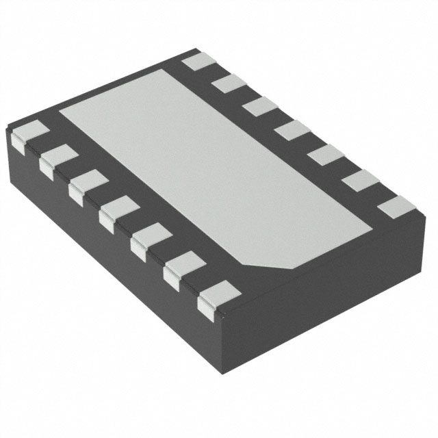


 工商网监
湘ICP备2023018690号
工商网监
湘ICP备2023018690号

