TLK1101E
www.ti.com
SLLS845A – AUGUST 2007 – REVISED OCTOBER 2007
11.3-Gbps Cable and PC Board Equalizer
FEATURES
APPLICATIONS
•
•
•
1
•
•
•
•
•
•
•
•
Multi-Rate Operation up to 11.3Gbps
Compensates for up to 30dB Loss on the
Receive Side and up to 7dB Loss on the
Transmit Side at 5.65GHz
Input Offset Cancellation
Output Disable/Squelch Function
Loss Of Signal Detection
Adjustable Output Swing
Adjustable Output De-Emphasis
Two-Wire Serial Interface
Single 3.3V Supply
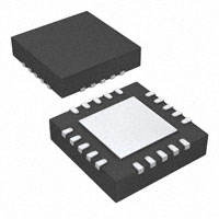
Surface Mount Small Footprint 4-mm × 4-mm
20-Pin QFN Package
•
•
High-Speed Links In Communication And Data
Systems
SFP+ and XFP Active Cables
Backplane, Daughtercard, and Cable
Interconnects for 10GE, 8GFC, 10GFC, 10G
SONET, SAS, SATA
100 Ω Differential
100Ω
differential
PCB interconnect
Interconnect
Up to 11.3Gbps
Differential
Input Data
Input AC Coupling
Up to 20-meter
20 -meter100Ω
100 Ω
Cable or Equivalent
Backplane Link
TLK1101E
Input AC Coupling
Output AC Coupling
TLK1101E
Output AC Coupling
Up to 11.3Gbps
Differential
Output Data
100 Ω Differential
100Ω
differential
interconnect
PCB Interconnect
DESCRIPTION
The TLK1101E is a versatile and flexible high-speed equalizer for applications in digital high-speed links with
data rates up to 11.3Gbps.
The TLK1101E can be configured in many ways to optimize its performance. It provides output de-emphasis
adjustable from 0dB to 7dB using pins DE0 and DE1.
The output differential voltage swing can be set to 300mVp-p, 600mVp-p, or 900mVp-p using the SWG pin. A
controlling voltage on pin VTH can be used to adjust the input threshold voltage.
Pins LN0 and LN1 can be used to optimize the device performance for various interconnect lengths, e.g. from 0
to 20 meters of 24-AWG twinaxial cable.
The LOS (loss of signal) assert level can be set to a desired level through a controlling voltage connected to pin
LOSL. The LOS assert levels can be chosen from two LOS assert level ranges selectable with the LOSR pin.
1
Please be aware that an important notice concerning availability, standard warranty, and use in critical applications of
Texas Instruments semiconductor products and disclaimers thereto appears at the end of this data sheet.
PRODUCTION DATA information is current as of publication date.
Products conform to specifications per the terms of the Texas
Instruments standard warranty. Production processing does not
necessarily include testing of all parameters.
Copyright © 2007, Texas Instruments Incorporated
�TLK1101E
www.ti.com
SLLS845A – AUGUST 2007 – REVISED OCTOBER 2007
The output can be disabled using the DIS pin. The DIS and the LOS pin can be connected together to implement
a squelch function.
The de-emphasis, the output voltage swing, the input threshold voltage, the output disable, and the LOS assert
levels and ranges can alternatively be set using the two-wire serial interface through the SCL and SDA pins. The
external pin configuration is the default device setup method. The active device control method is selected
through register address 0 bit 0 (see Table 4 and Table 20). The two-wire serial interface also allows for the
control of the input bandwidth to optimize the device performance for various data rates.
The high input signal dynamic range ensures low jitter output signals even when overdriven with input signal
swings as high as 1600mVp-p differential.
The low-frequency cut-off is low enough to support low-frequency control signals such as SAS and SATA
out-of-band (OOB) signals.
BLOCK DIAGRAM
A simplified block diagram of the TLK1101E is shown in Figure 1. This compact, low power, 11.3-Gbps equalizer
consists of a high-speed data path with offset cancellation block combined with an analog input threshold
selection circuitry, a loss of signal detection block, a two-wire interface with a control-logic block, a bandgap
voltage reference, and a bias current generation block.
VCC
GND
Offset
Cancellation
VCC
50W
50W
Input Buffer
with
Selectable
Bandwidth
Output
Buffer
Output
Driver
Equalizer
Stage
DIN+
VCC
50W
DOUT+
DOUT-
DIN-
LOS
Loss of Signal
Detection
SDA
50W
SDA
8-Bit Register
Control Settings
Input Threshold
4-Bit
De-emphasis
2-Bit Output Swing
4-Bit + Select
Input Bandwidth
8-Bit Register
SCL
SCL
DIS
DIS
LN0
LN 0
LN1
LN1
LOSR
LOSR
LOSL
LOSL
SWG
SWG
VTH
VTH
DE0
DE 0
DE1
DE 1
7-Bit + Select
4-Bit
7-Bit Register
LOS Assert Level
SEL_RATE
SEL_LOSL
Band-Gap Voltage
Reference and
Bias Current
Generation
Power-On
Reset
2-Wire Interface &
Control Logic
Figure 1. Simplified Block Diagram of the TLK1101E
2
Submit Documentation Feedback
Copyright © 2007, Texas Instruments Incorporated
Product Folder Link(s): TLK1101E
�TLK1101E
www.ti.com
SLLS845A – AUGUST 2007 – REVISED OCTOBER 2007
PACKAGE
For the TLK1101E a small footprint 4-mm × 4-mm 20-pin QFN package is used, with a lead pitch of 0.5mm. The
pin-out is shown in Figure 2.
19 18 17 16
LN1
DE1
20
LN0
DE0
SWG
RGP PACKAGE
(TOP VIEW)
GND 1
15
DIN+
14 DOUT+
2
DIN– 3
VCC
13 DOUT–
TLK1101E
12 VCC
GND 4
EP
6
7
8
9
10
VTH
SDA
SCL
DIS
LOS
LOSL 5
11 LOSR
Figure 2. Pin-Out of the TLK1101E in a 4-mm × 4-mm 20-Pin QFN Package
TERMINAL FUNCTIONS
PIN
SYMBOL
1, 4
GND
supply
Circuit ground.
2
DIN+
analog-in
Non-inverted data input. On-chip 50Ω terminated to VCC.
3
DIN–
analog-in
Inverted data input. On-chip 50Ω terminated to VCC.
5
LOSL
analog-in
LOS threshold control. A controlling voltage on this pin adjusts the LOS assert and de-assert levels.
6
VTH
analog-in
Input signal threshold control. A controlling voltage of 0V to 1V on this pin adjusts the input signal
threshold. Leave open for the default 0V differential threshold.
7
SDA
digital-in/out
Bidirectional serial data pin for the SDA/SCL interface. Open drain. Always connect to a pull-up
resistor.
8
SCL
digital-in
Serial clock pin for the SDA/SCL interface. Always connect to a pull-up resistor.
9
DIS
digital-in
Disables CML output stage when set to high level. Internally pulled down.
10
LOS
digital-out
High level indicates that the input signal amplitude is below the programmed threshold level. Open
drain. Requires an external 10kΩ pull-up resistor to VCC for proper operation.
11
LOSR
digital-in
LOS range select. Set to high level or leave open for upper range, or set to low level for lower range.
12, 15
TYPE
DESCRIPTION
VCC
supply
3.3V ± 10% supply voltage.
13
DOUT–
CML-out
Inverted data output. On-chip 50Ω back-terminated to VCC.
14
DOUT+
CML-out
Non-inverted data output. On-chip 50Ω back-terminated to VCC.
16
SWG
three-state
Output voltage swing control. Set to high level for high swing, set to low level for low swing, or leave
open for medium swing.
17
LN1
digital-in
Interconnect length select. Supports two logic levels: high and low. (see Table 2)
18
LN0
digital-in
19
DE1
three-state
20
DE0
three-state
EP
EP
Output signal de-emphasis control. Supports three logic levels: high, low, and open. (see Table 1)
Exposed die pad (EP) must be grounded.
Submit Documentation Feedback
Copyright © 2007, Texas Instruments Incorporated
Product Folder Link(s): TLK1101E
3
�TLK1101E
www.ti.com
SLLS845A – AUGUST 2007 – REVISED OCTOBER 2007
ABSOLUTE MAXIMUM RATINGS
over operating free-air temperature range (unless otherwise noted)
(1)
VALUE
UNIT
–0.3 to 4.0
V
0.5 to 4.0
V
–0.3 to 4.0
V
±2.5
V
VCC
Supply voltage (2)
VDIN+, VDIN–
Voltage at DIN+, DIN–
VDIS, VLOSL, VLOSR, VTH, VDE0, VDE1, VLN0,
VLN1, VSWG, VSCL, VSDA
Voltage at DIS, LOSL, LOSR, VTH, DE0, DE1, LN0, LN1,
SWG, SCL, SDA (2)
VDIN,DIFF
Differential voltage between DIN+ and DIN–
IDIN+, IDIN–, IDOUT+, IDOUT–
Continuous current at inputs and outputs
–25 to 25
mA
ESD
ESD Rating at all pins
2.5
kV (HBM)
TJ,max
Maximum junction temperature
125
°C
(1)
(2)
(2)
Stresses beyond those listed under absolute maximum ratings may cause permanent damage to the device. These are stress ratings
only. Functional operation of the device at these or any other conditions beyond those indicated under recommended operating
conditions is not implied. Exposure to absolute–maximum–rated conditions for extended periods may affect device reliability.
All voltage values are with respect to network ground terminal.
RECOMMENDED OPERATING CONDITIONS
MIN
NOM
MAX
VCC
Supply voltage
2.95
3.3
3.6
UNIT
V
TA
Operating lead temperature
–40
100
°C
VIH
CMOS Input high voltage
2.0
VIL
CMOS Input low voltage
V
0.8
V
DC ELECTRICAL CHARACTERISTICS
over recommended operating conditions (unless otherwise noted)
PARAMETER
VCC
TEST CONDITIONS
MIN
TYP
MAX
2.95
3.3
3.6
SWG = Open (CML output current included)
76
110
SWG = High (CML output current included)
83
120
Supply voltage
ICC
Supply current
LOS High voltage
ISOURCE = 50µA; 10kΩ Pull-up to VCC on LOS pin
LOS Low voltage
ISINK = 10mA; 10kΩ Pull-up to VCC on LOS pin
2.4
UNIT
V
mA
V
0.4
V
AC ELECTRICAL CHARACTERISTICS
Typical operating condition is at VCC = 3.3V and TA = 25°C. Over recommended operating conditions (unless otherwise noted)
PARAMETER
VIN,MIN
VIN,MAX
VOD
(1)
4
TEST CONDITIONS
Low frequency –3dB bandwidth
With 0.1µF input AC-coupling capacitors
Data input sensitivity (1)
BER < 10–12 , K28.5 Pattern at 11.3Gbps over a 15-m
24-AWG cable including two SMA connectors,
SWG = Open, No de-emphasis, Maximum interconnect
length setting. Voltage measured at the input of the cable
Data input overload
BER < 10–12 , K28.5 Pattern at 11.3Gbps, K28.5 pattern
at 11.3Gbps over a 15-m 24-AWG cable including two
SMA connectors, SWG = Open, No de-emphasis,
Maximum interconnect length setting. Voltage measured
at the input of the cable
High frequency boost
f = 5.65GHz
Differential data output voltage
swing
MIN
TYP
MAX
UNIT
30
50
kHz
250
mVp-p
1600
mVp-p
20
24
DIS = Low, SWG = Low, VIN = 400mVp-p,
No de-emphasis, No interconnect line
dB
225
300
450
DIS = Low, SWG = Open, VIN = 400mVp-p,
No de-emphasis, No interconnect line
450
600
800
DIS = Low, SWG = High, VIN = 400mVp-p,
No de-emphasis, No interconnect line
600
900
1200
mVp-p
The given differential input signal swing is valid for the low-frequency components of the input signal. The high frequency components
may be attenuated by up to 24dB at 5.65GHz.
Submit Documentation Feedback
Copyright © 2007, Texas Instruments Incorporated
Product Folder Link(s): TLK1101E
�TLK1101E
www.ti.com
SLLS845A – AUGUST 2007 – REVISED OCTOBER 2007
AC ELECTRICAL CHARACTERISTICS (continued)
Typical operating condition is at VCC = 3.3V and TA = 25°C. Over recommended operating conditions (unless otherwise noted)
PARAMETER
TEST CONDITIONS
MIN
TYP
MAX
VCC–0.113
VCC–0.075
VCC–0.056
DIS = Low, SWG = Open, VIN = 400mVp-p,
No de-emphasis, No interconnect line
VCC–0.2
VCC–0.15
VCC–0.113
DIS = Low, SWG = High, VIN = 400mVp-p,
No de-emphasis, No interconnect line
VCC–0.3
VCC–0.225
VCC–0.15
1.5
5
DIS = Low, SWG = Low, VIN = 400mVp-p,
No de-emphasis, No interconnect line
VCM,OUT
VRIP
Data output common-mode voltage
Differential output ripple
Output de-emphasis (2)
DE
DJ
Deterministic jitter
RJ
Random jitter
DIS = High, 50% Transitions of K28.5 pattern at
11.3Gbps, No interconnect line, VIN = 1600mVp-p
K28.5 Pattern at 11.3Gbps, No interconnect line,
VIN = 400mVp-p, SWG = Open, Output de-emphasis off:
DE0 = Low, DE1 = Low
0
K28.5 Pattern at 11.3Gbps, No interconnect line,
VIN = 400mVp-p, SWG = Open, Maximum output
de-emphasis: DE0 = High, DE1 = High
7
K28.5 Pattern at 11.3Gbps, 10-m 28-AWG Cable,
VIN = 400mVp-p, SWG = Open, No de-emphasis,
Maximum interconnect length setting
12
K28.5 Pattern at 11.3Gbps, 15-m 24-AWG Cable,
VIN = 400mVp-p, SWG = Open, No de-emphasis,
Maximum interconnect length setting
12
K28.5 Pattern at 11.3Gbps, 10-m 28-AWG Cable,
VIN = 400mVp-p, SWG = Open, No de-emphasis,
Maximum interconnect length setting
1.0
K28.5 Pattern at 11.3Gbps, 15-m 24-AWG Cable,
VIN = 400mVp-p, SWG = Open, No de-emphasis,
Maximum interconnect length setting
1.0
psRMS
20% to 80%, No interconnect line,
VIN = 400mVp-p, SWG = Open, No de-emphasis
20
28
tF
Output fall time
20% to 80%, No interconnect line,
VIN = 400mVp-p, SWG = Open, No de-emphasis
20
28
SDD11
Differential input return loss
SDD22
Differential output return loss
SCD11
Input differential to common-mode
conversion
SCC22
Common-mode output return loss
VDAS
LOS De-assert threshold voltage
LOS Hysteresis
TAS/DAS
LOS Assert/de-assert time
TDIS
Disable response time
Latency
(2)
(3)
ps
0.01GHz < f < 3.9GHz
16
3.9GHz < f < 12.1GHz
See
0.01GHz < f < 3.9GHz
dB
(3)
16
3.9GHz < f < 12.1GHz
See
dB
(3)
0.01GHz < f < 7.5GHz
25
7.5GHz < f < 12.1GHz
20
0.01GHz < f < 2.5GHz
13
2.5GHz < f < 12.1GHz
7
K28.5 Pattern at 11.3Gbps, No interconnect,
LOSR = High, LOSL = Open
25
60
K28.5 Pattern at 11.3Gbps, No interconnect,
LOSR = High, LOSL = 1.0V
75
180
dB
dB
mVp-p
K28.5 Pattern at 11.3Gbps, No interconnect,
LOSR = High, LOSL = Open
100
150
K28.5 Pattern at 11.3Gbps, No interconnect,
LOSR = High, LOSL = 1.0V
300
450
20log(VDAS / VAS)
mVp-p
2.5
4.5
2.5
From DIN+/DIN– to DOUT+/DOUT–
mVRMS
psp-p
Output rise time
LOS Assert threshold voltage
V
dB
tR
VAS
UNIT
dB
50
µs
20
ns
150
ps
See Table 1 and Figure 3 for output de-emphasis settings
Differential Return Loss given by SDD11, SDD22 = 19.3 + 26.66 log10(f/8.25), f in GHz
Submit Documentation Feedback
Copyright © 2007, Texas Instruments Incorporated
Product Folder Link(s): TLK1101E
5
�TLK1101E
www.ti.com
SLLS845A – AUGUST 2007 – REVISED OCTOBER 2007
Table 1. Available Output De-emphasis Settings
DE0
DE1
LOW
OPEN
HIGH
LOW
0dB
0.875dB
1.75dB
OPEN
2.625dB
3.5dB
4.375dB
HIGH
5.25dB
6.125dB
7dB
A
VL, p–p
t
0
t
VH, p–p
é æ VL, p-p öù
÷ú
DE = 20 × êlogç
êë çè VH, p-p ÷øúû
–A
T0157-01
Figure 3. Output De-emphasis
Table 2. Available Interconnect Length Settings (24-AWG Twinaxial Cable Used as Reference)
LN0
LN1
6
LOW
HIGH
LOW
0–5 meters
10–15 meters
HIGH
5–10 meters
15–20 meters
Submit Documentation Feedback
Copyright © 2007, Texas Instruments Incorporated
Product Folder Link(s): TLK1101E
�TLK1101E
www.ti.com
SLLS845A – AUGUST 2007 – REVISED OCTOBER 2007
TWO-WIRE SERIAL INTERFACE AND CONTROL LOGIC
FUNCTIONAL DESCRIPTION
The TLK1101E uses a two-wire serial interface for digital control. The two circuit inputs, SDA and SCL, are
driven, respectively, by the serial data and serial clock from a microcontroller, for example. Both inputs include
100kΩ pull-up resistors to VCC. For driving these inputs, an open-drain output is recommended.
The two-wire interface allows write access to the internal memory map to modify control registers and read
access to read out control and status signals. The TLK1101E is a slave device only which means that it cannot
initiate a transmission itself; it always relies on the availability of the SCL signal for the duration of the
transmission. The master device provides the clock signal as well as the START and STOP commands. The
protocol for a data transmission is as follows:
1. START command
2. 7-bit slave address (0101000) followed by an eighth bit which is the data direction bit (R/W). A zero indicates
a WRITE and a 1 indicates a READ.
3. 8-bit register address
4. 8-bit register data
5. STOP command
Regarding timing, the TLK1101E is I2C-compatible. The typical timing is shown in Figure 4 and a complete data
transfer is shown in Figure 5. Parameters for Figure 4 are defined in Table 3.
Bus Idle: Both SDA and SCL lines remain HIGH
Start Data Transfer: A change in the state of the SDA line, from HIGH to LOW, while the SCL line is HIGH,
defines a START condition (S). Each data transfer is initiated with a START condition.
Stop Data Transfer: A change in the state of the SDA line from LOW to HIGH while the SCL line is HIGH
defines a STOP condition (P). Each data transfer is terminated with a STOP condition; however, if the master still
wishes to communicate on the bus, it can generate a repeated START condition and address another slave
without first generating a STOP condition.
Data Transfer: The number of data bytes transferred between a START and a STOP condition is not limited and
is determined by the master device. The receiver acknowledges the transfer of data.
Acknowledge: Each receiving device, when addressed, is obliged to generate an acknowledge bit. The
transmitter releases the SDA line and a device that acknowledges must pull down the SDA line during the
acknowledge clock pulse in such a way that the SDA line is stable LOW during the HIGH period of the
acknowledge clock pulse. Setup and hold times must be taken into account. When a slave-receiver does not
acknowledge the slave address, the data line must be left HIGH by the slave. The master can then generate a
STOP condition to abort the transfer. If the slave-receiver does acknowledge the slave address but some time
later in the transfer cannot receive any more data bytes, the master must abort the transfer. This is indicated by
the slave generating the not acknowledge on the first byte to follow. The slave leaves the data line HIGH and the
master generates the STOP condition.
SDA
tBUF
tLOW
tr
tHIGH
tf
tHDSTA
SCL
P
S
S
tHDSTA
tHDDAT
tSUDAT
P
tSUSTA
tSUSTO
Figure 4. Two-Wire Serial Interface Timing Diagram.
Submit Documentation Feedback
Copyright © 2007, Texas Instruments Incorporated
Product Folder Link(s): TLK1101E
7
�TLK1101E
www.ti.com
SLLS845A – AUGUST 2007 – REVISED OCTOBER 2007
Table 3. Two-Wire Serial Interface Timing Diagram Definitions
SYMBOL
PARAMETER
MIN
MAX
UNIT
fSCL
SCL Clock frequency
tBUF
Bus free time between START and STOP conditions
1.3
400
kHz
µs
tHDSTA
Hold time after repeated START condition. After this period, the first clock pulse is generated
0.6
µs
tLOW
Low period of the SCL clock
1.3
µs
tHIGH
High period of the SCL clock
0.6
µs
tSUSTA
Setup time for a repeated START condition
0.6
µs
tHDDAT
Data HOLD time
0
µs
tSUDAT
Data setup time
tR
Rise time of both SDA and SCL signals
300
ns
tF
Fall time of both SDA and SCL signals
300
ns
tSUSTO
Setup time for STOP condition
100
ns
µs
0.6
SDA
SCL
1-7
S
SLAVE
ADDRESS
8
R/W
9
ACK
1-7
8
REGISTER
ADDRESS
9
ACK
8
1-7
REGISTER
FUNCTION
9
ACK
P
Figure 5. Two-Wire Serial Interface Data Transfer
8
Submit Documentation Feedback
Copyright © 2007, Texas Instruments Incorporated
Product Folder Link(s): TLK1101E
�TLK1101E
www.ti.com
SLLS845A – AUGUST 2007 – REVISED OCTOBER 2007
REGISTER MAPPING
The register mapping for read/write register addresses 0 (0x00) through 13 (0x0D) are shown in Table 4 through
Table 17. The register mapping for the read only register addresses 14 (0x0E) and 15 (0x0F) are shown in
Table 18 and Table 19. Table 20 describes the circuit functionality based on the register settings.
Table 4. Register 0 (0x00) Mapping – Control Settings
register address 0 (0x00)
bit 7
bit 6
bit 5
bit 4
bit 3
bit 2
bit 1
bit 0
REG11OFF
REG3OFF
REG2OFF
REG1OFF
DISABLE
LOS_RNG
OCOFF
I2CMODE
Table 5. Register 1 (0x01) Mapping – Input Threshold Adjust
register address 1 (0x01)
bit 7
bit 6
bit 5
bit 4
bit 3
bit 2
bit 1
bit 0
THRESH7
THRESH6
THRESH5
THRESH4
THRESH3
THRESH2
THRESH1
THRESH0
Table 6. Register 2 (0x02) Mapping – De-emphasis Setting
register address 2 (0x02)
bit 7
bit 6
bit 5
bit 4
bit 3
bit 2
bit 1
bit 0
–
–
–
–
DEEM3
DEEM2
DEEM1
DEEM0
Table 7. Register 3 (0x03) Mapping – Output Swing Control
register address3 (0x03)
bit 7
bit 6
bit 5
bit 4
bit 3
bit 2
bit 1
bit 0
–
–
–
–
–
–
AMP1
AMP0
Table 8. Register 4 (0x04) Mapping
register address 4 (0x04)
bit 7
bit 6
bit 5
bit 4
bit 3
bit 2
bit 1
bit 0
–
–
–
–
–
–
–
–
Table 9. Register 5 (0x05) Mapping
register address 5 (0x05)
bit 7
bit 6
bit 5
bit 4
bit 3
bit 2
bit 1
bit 0
–
–
–
–
–
–
–
–
Table 10. Register 6 (0x06) Mapping
register address 6 (0x06)
bit 7
bit 6
bit 5
bit 4
bit 3
bit 2
bit 1
bit 0
–
–
–
–
–
–
–
–
Table 11. Register 7 (0x07) Mapping – Maximum Data Rate Setting
register address 7 (0x07)
bit 7
bit 6
bit 5
bit 4
bit 3
bit 2
bit 1
bit 0
RATE_7
–
–
–
RATE_3
RATE_2
RATE_1
RATE_0
Submit Documentation Feedback
Copyright © 2007, Texas Instruments Incorporated
Product Folder Link(s): TLK1101E
9
�TLK1101E
www.ti.com
SLLS845A – AUGUST 2007 – REVISED OCTOBER 2007
Table 12. Register 8 (0x08) Mapping
register address 8 (0x08)
bit 7
bit 6
bit 5
bit 4
bit 3
bit 2
bit 1
bit 0
–
–
–
–
–
–
–
–
Table 13. Register 9 (0x09) Mapping
register address 9 (0x09)
bit 7
bit 6
bit 5
bit 4
bit 3
bit 2
bit 1
bit 0
–
–
–
–
–
–
–
–
Table 14. Register 10 (0x0A) Mapping
register address 10 (0x0A)
bit 7
bit 6
bit 5
bit 4
bit 3
bit 2
bit 1
bit 0
–
–
–
–
–
–
–
–
Table 15. Register 11 (0x0B) Mapping – LOS Level Setting
register address 11 (0x0B)
bit 7
bit 6
bit 5
bit 4
bit 3
bit 2
bit 1
bit 0
LOSLVL_7
LOSLVL_6
LOSLVL_5
LOSLVL_4
LOSLVL_3
LOSLVL_2
LOSLVL_1
LOSLVL_0
Table 16. Register 12 (0x0C) Mapping
register address 12 (0x0C)
bit 7
bit 6
bit 5
bit 4
bit 3
bit 2
bit 1
bit 0
–
–
–
–
–
–
–
–
Table 17. Register 13 (0x0D) Mapping
register address 13 (0x0D)
bit 7
bit 6
bit 5
bit 4
bit 3
bit 2
bit 1
bit 0
–
–
–
–
–
–
–
–
Table 18. Register 14 (0x0E) Mapping – Selected Rate Setting (Read Only)
register address 14 (0x0E)
bit 7
bit 6
bit 5
bit 4
bit 3
bit 2
bit 1
bit 0
–
–
–
–
SEL_RATE3
SEL_RATE2
SEL_RATE1
SEL_RATE0
Table 19. Register 15 (0x0F) Mapping – Selected LOS Level (Read Only)
register address 15 (0x0F)
10
bit 7
bit 6
bit 5
bit 4
bit 3
bit 2
bit 1
bit 0
–
SEL_LOSL6
SEL_LOSL5
SEL_LOSL4
SEL_LOSL3
SEL_LOSL2
SEL_LOSL1
SEL_LOSL1
Submit Documentation Feedback
Copyright © 2007, Texas Instruments Incorporated
Product Folder Link(s): TLK1101E
�TLK1101E
www.ti.com
SLLS845A – AUGUST 2007 – REVISED OCTOBER 2007
Table 20. Register Functionality
NAME
REGISTER DESCRIPTION
FUNCTION
REG11OFF
Address 0 bit 7:
Register address 11 control
Register address 11 control bit:
1 = External LOS level (LOSL) control active
0 = Register address 11 settings active (default)
REG3OFF
Address 0 bit 6:
Register address 3 control
Register address 3 control bit:
1 = External output swing (SWG) control active
0 = Register address 3 settings active (default)
REG2OFF
Address 0 bit 5:
Register address 2 control
Register address 2 control bit:
1 = External output de-emphasis (DE) control active
0 = Register address 2 settings active (default)
REG1OFF
Address 0 bit 4:
Register address 1 control
Register address 1 control bit:
1 = External input threshold (VTH) control active
0 = Register address 1 settings active (default)
DISABLE
Address 0 bit 3:
Output disable
Output disable bit:
1 = Output disabled
0 = Output enabled (default)
LOS_RNG
Address 0 bit 2:
LOS Range
LOS Range bit:
1 = High LOS assert voltage range
0 = Low LOS assert voltage range (default)
OCOFF
Address 0 bit 1:
Offset cancellation disable
Offset cancellation disable bit:
1 = Offset cancellation is disabled
0 = Offset cancellation is enabled (default)
I2CMODE
Address 0 bit 0:
Two-wire interface disable
Two-wire interface disable bit:
1 = Register settings active
0 = External control active (default)
THRESH7
Address 1 bit 7:
Input threshold adjust bit 7 (MSB)
THRESH6
Address 1 bit 6:
Input threshold adjust bit 6
THRESH5
Address 1 bit 5:
Input threshold adjust bit 5
Input threshold adjustment setting:
Maximum positive shift for 00000001 (1)
Minimum positive shift for 01111111 (127)
Zero shift for 10000000 (128) or 00000000 (0) (default)
Minimum negative shift for 10000001 (129)
Maximum negative shift for 11111111 (255)
THRESH4
Address 1 bit 4:
Input threshold adjust bit 4
THRESH3
Address 1 bit 3:
Input threshold adjust bit 3
THRESH2
Address 1 bit 2:
Input threshold adjust bit 2
THRESH1
Address 1 bit 1:
Input threshold adjust bit 1
THRESH0
Address 1 bit 0:
Input threshold adjust bit 0 (LSB)
DEEM3
Address 2 bit 3:
De-emphasis adjust bit 3 (MSB)
DEEM2
De-emphasis (dB)
Register Setting
0
0000 (default)
0.875
0001
Address 2 bit 1:
1.75
0011
De-emphasis adjust bit 1
2.625
0100
3.5
0101
4.375
0111
5.25
1100
6.125
1101
7
1111
Address 2 bit 2:
De-emphasis adjust bit 2
DEEM1
DEEM0
De-emphasis setting:
Address 2 bit 0:
De-emphasis adjust bit 0 (LSB)
Submit Documentation Feedback
Copyright © 2007, Texas Instruments Incorporated
Product Folder Link(s): TLK1101E
11
�TLK1101E
www.ti.com
SLLS845A – AUGUST 2007 – REVISED OCTOBER 2007
Table 20. Register Functionality (continued)
NAME
REGISTER DESCRIPTION
FUNCTION
AMP1
Address 3 bit 1:
Output swing control bit 1 (MSB)
AMP0
Address 3 bit 0:
Output swing control bit 0 (LSB)
RATE_7
Address 7 bit 7:
Bandwidth selection bit 7 (MSB)
RATE_3
Address 7 bit 3:
Bandwidth selection bit 3
RATE_2
Address 7 bit 2:
Bandwidth selection bit 2
RATE_1
Address 7 bit 1:
Bandwidth selection bit 1
RATE_0
Address 7 bit 0:
Bandwidth selection bit 0 (LSB)
LOSLVL_7
Address 11 bit 7:
LOS assert level bit 7 (MSB)
LOSLVL_6
Address 11 bit 6:
LOS assert level selection bit 6
LOSLVL_5
Address 11 bit 5:
LOS assert level selection bit 5
LOSLVL_4
Address 11 bit 4:
LOS assert level selection bit 4
LOSLVL_3
Address 11 bit 3:
LOS assert level selection bit 3
LOSLVL_2
Address 11 bit 2:
LOS assert level selection bit 2
LOSLVL_1
Address 11 bit 1:
LOS assert level selection bit 1
LOSLVL_0
Address 11 bit 0:
LOS assert level selection bit 0 (LSB)
SEL_RATE3
Address 14 bit 3:
Selected rate setting bit 3
SEL_RATE2
Address 14 bit 2:
Selected rate setting bit 2
SEL_RATE1
Address 14 bit 1:
Selected rate setting bit 1
SEL_RATE0
Address 14 bit 0:
Selected rate setting bit 0
12
Output swing control:
00 = 300mVp-p
01 = 600mVp-p (default)
10 = 600mVp-p
11 = 900mVp-p
Input filter bandwidth selection control bit:
1 = Contents of register address 7 bits 3 to 0 are used to select the input filter
bandwidth
0 = Bandwidth of 9.1GHz is used (default)
Input filter bandwidth selection bits:
Register 7 bits 3 to 0 are used to set the input filter bandwidth:
0000 = Maximum bandwidth
1111 = Minimum bandwidth
LOS Assert level control bit:
1 = Contents of register address 11 bits 6 to 0 are used to select the LOS assert
level
0 = LOS Assert level of 50mVp-p is used (default)
LOS Assert level selection bits:
Register 11 bits 6 to 0 are used to select the LOS assert level:
0000000 = Minimum LOS assert level
1111111 = Maximum LOS assert level
Selected rate setting (read only)
Submit Documentation Feedback
Copyright © 2007, Texas Instruments Incorporated
Product Folder Link(s): TLK1101E
�TLK1101E
www.ti.com
SLLS845A – AUGUST 2007 – REVISED OCTOBER 2007
Table 20. Register Functionality (continued)
NAME
REGISTER DESCRIPTION
FUNCTION
SEL_LOSL6
Address 15 bit 6:
Selected LOS assert level bit 6 (MSB)
SEL_LOSL5
Address 15 bit 5:
Selected LOS assert level bit 5
SEL_LOSL4
Address 15 bit 4:
Selected LOS assert level bit 4
SEL_LOSL3
Address 15 bit 3:
Selected LOS assert level bit 3
SEL_LOSL2
Address 15 bit 2:
Selected LOS assert level bit 2
SEL_LOSL1
Address 15 bit 1:
Selected LOS assert level bit 1
SEL_LOS_0
Address 15 bit 0:
Selected LOS assert level bit 0 (LSB)
Selected LOS assert level (read only)
Submit Documentation Feedback
Copyright © 2007, Texas Instruments Incorporated
Product Folder Link(s): TLK1101E
13
�TLK1101E
www.ti.com
SLLS845A – AUGUST 2007 – REVISED OCTOBER 2007
TYPICAL CHARACTERISTICS
Typical operating condition is at VCC = 3.3V and TA = 25°C, VIN = 400mVp-p, DE0 = DE1 = low, SWG = open,
LN0 = LN1 = high, and no interconnect line at the output (unless otherwise noted). Differential S-parameter
characteristics of Spectra-Strip SkewClear EXD twinaxial cables and a 36-inch FR-4 stripline used for the
measurements captured in this document are as shown in Figure 6.
0
Differential S-Parameter Magnitude (dB)
-10
-20
-30
-40
-50
Insertion Loss - 15m 24AWG Cable
-60
Insertion Loss - 10m 28AWG Cable
Insertion Loss - 36in 12mil Stripline
-70
Return Loss - 15m 24AWG Cable
Return Loss - 10m 28AWG Cable
-80
Return Loss - 36in 12mil Stripline
-90
0
1
2
3
4
5
6
7
8
9
10
11
12
13
14
15
16
17
18
19
20
Frequency (GHz)
Figure 6. Typical Differential S-Parameter Characteristics of Interconnect Lines
14
Submit Documentation Feedback
Copyright © 2007, Texas Instruments Incorporated
Product Folder Link(s): TLK1101E
�TLK1101E
www.ti.com
SLLS845A – AUGUST 2007 – REVISED OCTOBER 2007
TYPICAL CHARACTERISTICS (continued)
DIFFERENTIAL EQUALIZER INPUT SIGNAL (TOP) AND OUTPUT SIGNAL (BOTTOM) AT
11.3Gbps USING A K28.5 PATTERN
12-mil Stripline
36-inch
12-mil Stripline
Output Voltage
200mV/Div
Output Voltage
200mV/Div
Input Voltage
100mV/Div
Input Voltage
100mV/Div
36-inch
Time − 40ps/Div
Time − 500ps/Div
10-meter 28-AWG Twinaxial Cable
Output Voltage
200mV/Div
Output Voltage
200mV/Div
Input Voltage
50mV/Div
Input Voltage
50mV/Div
10-meter 28-AWG Twinaxial Cable
Time − 40ps/Div
Time − 500ps/Div
15-meter 24-AWG Twinaxial Cable
Output Voltage
200mV/Div
Output Voltage
200mV/Div
Input Voltage
50mV/Div
Input Voltage
50mV/Div
15-meter 24-AWG Twinaxial Cable
Time − 40ps/Div
Time − 500ps/Div
G002
Figure 7. Equalizer Input and Output Signals with Different Interconnect Lines at 11.3Gbps
Submit Documentation Feedback
Copyright © 2007, Texas Instruments Incorporated
Product Folder Link(s): TLK1101E
15
�TLK1101E
www.ti.com
SLLS845A – AUGUST 2007 – REVISED OCTOBER 2007
TYPICAL CHARACTERISTICS (continued)
DIFFERENTIAL EQUALIZER INPUT SIGNAL (TOP) AND OUTPUT SIGNAL (BOTTOM) AT
10.3125Gbps USING A K28.5 PATTERN
12-mil Stripline
36-inch
12-mil Stripline
Output Voltage
200mV/Div
Output Voltage
200mV/Div
Input Voltage
100mV/Div
Input Voltage
100mV/Div
36-inch
Time − 40ps/Div
Time − 500ps/Div
10-meter 28-AWG Twinaxial Cable
Output Voltage
200mV/Div
Output Voltage
200mV/Div
Input Voltage
50mV/Div
Input Voltage
50mV/Div
10-meter 28-AWG Twinaxial Cable
Time − 40ps/Div
Time − 500ps/Div
15-meter 24-AWG Twinaxial Cable
Output Voltage
200mV/Div
Output Voltage
200mV/Div
Input Voltage
50mV/Div
Input Voltage
50mV/Div
15-meter 24-AWG Twinaxial Cable
Time − 40ps/Div
Time − 500ps/Div
G003
Figure 8. Equalizer Input and Output Signals with Different Interconnect Lines at 10.3125Gbps
16
Submit Documentation Feedback
Copyright © 2007, Texas Instruments Incorporated
Product Folder Link(s): TLK1101E
�TLK1101E
www.ti.com
SLLS845A – AUGUST 2007 – REVISED OCTOBER 2007
TYPICAL CHARACTERISTICS (continued)
DIFFERENTIAL EQUALIZER INPUT SIGNAL (TOP) AND OUTPUT SIGNAL (BOTTOM) AT
8.5Gbps USING A K28.5 PATTERN
36-inch
12-mil Stripline
Output Voltage
200mV/Div
Output Voltage
200mV/Div
Input Voltage
100mV/Div
12-mil Stripline
Input Voltage
100mV/Div
36-inch
Time − 40ps/Div
Time − 500ps/Div
Input Voltage
50mV/Div
10-meter 28-AWG Twinaxial Cable
Output Voltage
200mV/Div
Output Voltage
200mV/Div
Input Voltage
50mV/Div
10-meter 28-AWG Twinaxial Cable
Time − 40ps/Div
Time − 500ps/Div
Input Voltage
50mV/Div
15-meter 24-AWG Twinaxial Cable
Output Voltage
200mV/Div
Output Voltage
200mV/Div
Input Voltage
50mV/Div
15-meter 24-AWG Twinaxial Cable
Time − 40ps/Div
Time − 500ps/Div
G004
Figure 9. Equalizer Input and Output Signals with Different Interconnect Lines at 8.5Gbps.
Submit Documentation Feedback
Copyright © 2007, Texas Instruments Incorporated
Product Folder Link(s): TLK1101E
17
�TLK1101E
www.ti.com
SLLS845A – AUGUST 2007 – REVISED OCTOBER 2007
TYPICAL CHARACTERISTICS (continued)
RANDOM JITTER
vs
INPUT VOLTAGE
RESIDUAL DETERMINISTIC JITTER
vs
INPUT VOLTAGE
1.5
20
RJ - Random Jitter - psRMS
1.3
DJ - Residual Deterministic Jitter - ps
36inch x 12mil Stripline
15m 24AWG Twinaxial Cable
1.1
10m 28AWG Twinaxial Cable
0.9
0.7
No interconnect
0.5
0.3
19
No Interconnect
18
36inch x 12mil Stripline
15m 24AWG Twinaxial Cable
17
16
15
14
13
10m 28AWG Twinaxial Cable
12
11
10
0.1
0
18
500
1000
1500
VIN - Input Voltage - mVpp
2000
2500
0
500
1000
1500
VIN - Input Voltage - mVpp
2000
Figure 10.
Figure 11.
DIFFERENTIAL INPUT RETURN LOSS
vs
FREQUENCY
DIFFERENTIAL OUTPUT RETURN LOSS
vs
FREQUENCY
Figure 12.
Figure 13.
Submit Documentation Feedback
2500
Copyright © 2007, Texas Instruments Incorporated
Product Folder Link(s): TLK1101E
�TLK1101E
www.ti.com
SLLS845A – AUGUST 2007 – REVISED OCTOBER 2007
TYPICAL CHARACTERISTICS (continued)
LOS THRESHOLD VOLTAGE
vs
LOSL VOLTAGE (LOSR = HIGH)
8
400
350
7
350
Hysteresis
250
5
200
4
150
0.2
0.3
0.4
0.5
0.6
LOSL - Voltage - V
0.7
0.8
0.9
Assert
1
50
1
0
0
0
0
1
0.1
0.2
0.3
0.4
0.5
0.6
LOSL - Voltage - V
0.7
0.8
0.9
1
Figure 14.
Figure 15.
LOS THRESHOLD VOLTAGE
vs
REGISTER 11 (0x0B) SETTING (LOSR = LOW)
LOS THRESHOLD VOLTAGE
vs
REGISTER 11 (0x0B) SETTING (LOSR = HIGH)
8
400
8
350
7
350
7
300
6
300
6
Hysteresis
250
5
200
4
150
3
2
100
Assert
50
0
170
1
Deassert
0
180
190
200
210
220
Register 11 (0x0B) Setting
230
240
250
VTH - LOS Threshold Voltage - mVPP
400
Hysteresis - dB
VTH - LOS Threshold Voltage - mVPP
0.1
4
200
2
Assert
0
5
100
2
0
Hysteresis
250
3
Deassert
50
6
300
150
3
100
7
Deassert
Hysteresis - dB
6
8
250
5
Hysteresis
200
4
150
3
100
2
Deassert
50
Hysteresis - dB
300
VTH - LOS Threshold Voltage - mVPP
400
Hysteresis - dB
VTH - LOS Threshold Voltage - mVPP
LOS THRESHOLD VOLTAGE
vs
LOSL VOLTAGE (LOSR = LOW)
Assert
1
0
0
120 130 140 150 160 170 180 190 200 210 220 230 240 250
Register 11 (0x0B) Setting
Figure 16.
Figure 17.
Submit Documentation Feedback
Copyright © 2007, Texas Instruments Incorporated
Product Folder Link(s): TLK1101E
19
�TLK1101E
www.ti.com
SLLS845A – AUGUST 2007 – REVISED OCTOBER 2007
TYPICAL CHARACTERISTICS (continued)
LOS THRESHOLD VOLTAGE
vs
DATA RATE (LOSL = 1V, LOSR = HIGH)
6
400
6
350
5.8
350
5.8
5.6
Hysteresis
250
5.4
200
5.2
150
5
100
Deassert
4.8
Assert
4.6
50
0
0
1
2
3
4
5
6
7
8
9
Data Rate - Gbps
10
11
12
13
4.4
14
300
5.6
Deassert
5.4
250
200
5.2
Assert
150
5
Hysteresis
100
4.8
4.6
50
4.4
0
0
1
2
Figure 18.
20
Hysteresis - dB
300
VTH - LOS Threshold Voltage - mVPP
400
Hysteresis - dB
VTH - LOS Threshold Voltage - mVPP
LOS THRESHOLD VOLTAGE
vs
DATA RATE (LOSL = 1V, LOSR = LOW)
3
4
5
6
7
8
9
Data Rate - Gbps
10
11
12
13
14
Figure 19.
Submit Documentation Feedback
Copyright © 2007, Texas Instruments Incorporated
Product Folder Link(s): TLK1101E
�TLK1101E
www.ti.com
SLLS845A – AUGUST 2007 – REVISED OCTOBER 2007
Revision History
Changes from Original (August 2007) to Revision A ..................................................................................................... Page
•
•
•
•
•
•
•
•
•
•
Added external pin configuration information - default device setup method to description ................................................. 2
Changed LN0 to LN1 in terminal functions table ................................................................................................................... 3
Changed LN1 to LN0 in terminal functions table ................................................................................................................... 3
Changed DE0 to DE1 in terminal functions table .................................................................................................................. 3
Changed DE1 to DE0 in terminal functions table .................................................................................................................. 3
Deleted fixed input equalizer in high frequency boost test conditions................................................................................... 4
Added Twinaxial to Table 2 title............................................................................................................................................. 6
Changed scale on Figure 7.................................................................................................................................................. 15
Changed scale on Figure 8.................................................................................................................................................. 16
Changed scale on Figure 9.................................................................................................................................................. 17
Submit Documentation Feedback
Copyright © 2007, Texas Instruments Incorporated
Product Folder Link(s): TLK1101E
21
�PACKAGE OPTION ADDENDUM
www.ti.com
10-Dec-2020
PACKAGING INFORMATION
Orderable Device
Status
(1)
Package Type Package Pins Package
Drawing
Qty
Eco Plan
(2)
Lead finish/
Ball material
MSL Peak Temp
Op Temp (°C)
Device Marking
(3)
(4/5)
(6)
TLK1101ERGPR
ACTIVE
QFN
RGP
20
3000
RoHS & Green
NIPDAU
Level-2-260C-1 YEAR
-40 to 100
TLK
1101E
TLK1101ERGPT
ACTIVE
QFN
RGP
20
250
RoHS & Green
NIPDAU
Level-2-260C-1 YEAR
-40 to 100
TLK
1101E
(1)
The marketing status values are defined as follows:
ACTIVE: Product device recommended for new designs.
LIFEBUY: TI has announced that the device will be discontinued, and a lifetime-buy period is in effect.
NRND: Not recommended for new designs. Device is in production to support existing customers, but TI does not recommend using this part in a new design.
PREVIEW: Device has been announced but is not in production. Samples may or may not be available.
OBSOLETE: TI has discontinued the production of the device.
(2)
RoHS: TI defines "RoHS" to mean semiconductor products that are compliant with the current EU RoHS requirements for all 10 RoHS substances, including the requirement that RoHS substance
do not exceed 0.1% by weight in homogeneous materials. Where designed to be soldered at high temperatures, "RoHS" products are suitable for use in specified lead-free processes. TI may
reference these types of products as "Pb-Free".
RoHS Exempt: TI defines "RoHS Exempt" to mean products that contain lead but are compliant with EU RoHS pursuant to a specific EU RoHS exemption.
Green: TI defines "Green" to mean the content of Chlorine (Cl) and Bromine (Br) based flame retardants meet JS709B low halogen requirements of