User's Guide
SLLU186 – August 2013
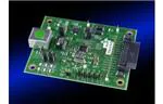
TLK111 Customer EVM
This user's guide details the design and operation of the evaluation module (EVM) for the TLK111.
1
2
3
4
Contents
TLK111 EVM Purpose and Content ...................................................................................... 1
1.1
EVM Use ............................................................................................................ 2
Information and Specifications ............................................................................................ 2
2.1
Usage Setup and Configuration .................................................................................. 2
2.2
Address Settings ................................................................................................... 2
2.3
TLK111CUSEVM Connections ................................................................................... 2
TLK111CUSEVM Specification ........................................................................................... 3
3.1
Overview ............................................................................................................ 3
3.2
Required Resources ............................................................................................... 3
3.3
Features ............................................................................................................. 3
3.4
TLK111CUSEVM Block Diagram ................................................................................ 4
3.5
PCB Physical Layout .............................................................................................. 5
3.6
EVM Schematics ................................................................................................... 6
3.7
Bill of Materials .................................................................................................... 12
Software .................................................................................................................... 15
List of Figures
1
EVM Block Diagram ........................................................................................................
4
2
EVM Layout ..................................................................................................................
5
3
TLK111CUSEVM Top Level Schematics ................................................................................
6
4
TLK111CUSEVM / TLK111 Schematics .................................................................................
7
5
TLK111CUSEVM 3.3V/1.5V LDO Schematics ..........................................................................
8
6
TLK111CUSEVM / SOR Schematics
....................................................................................
TLK111CUSEVM / MII Connector Schematics ........................................................................
TLK111CUSEVM / Magnetics Schematics.............................................................................
10
7
8
9
11
List of Tables
1
1
TLK111CUSEVM Connections ............................................................................................
2
TLK111CUSEVM Aneg Modes Connections ............................................................................
2
3
Bill of Materials.............................................................................................................
12
2
TLK111 EVM Purpose and Content
The Industrial Ethernet TLK111CUSEVM provides Texas Instruments customers a platform to quickly
design and market systems containing the TLK111 device. Customers are encouraged to copy EVM
components to expedite their design process. The TLK111CUSEVM operates with only a single voltage
(5V from the MII). All other voltages are internally produced.
The EVM kit contains:
• TLK111CUSEVM unit
• Printed copy of this user's guide
• TLK111CUSEVM schematic
SLLU186 – August 2013
Submit Documentation Feedback
TLK111 Customer EVM
Copyright © 2013, Texas Instruments Incorporated
1
�Information and Specifications
1.1
www.ti.com
EVM Use
The TLK111 supports an IEEE 802.3u 100BASE-FX Fiber Interface. This ability was not implemented in
this customer EVM. For fiber performance evaluation, a new customer EVM is being developed.
2
Information and Specifications
This section contains the specifications of the TLK111CUSEVM card, as well as a description of the card's
interfaces, connectors, jumpers, and LEDs.
2.1
Usage Setup and Configuration
Power for the TLK111CUSEVM is supplied via a MII connector.
• If 5V is supplied, the on-board voltage regulator, U1, converts 5V to 3.3V for the device.
• If 3.3V is supplied from the MII connector, assemble R59 and remove R56.
• Make sure the J2 jumper is installed in order to supply 3.3V to the magnetic CT.
• Make sure J1 jumper is installed and configured to MII or RMII.
2.2
Address Settings
The PMD address TLK111CUSEVM Physical Layer device is set by the following jumpers:
• J7: PHY ID [0]
• J6: PHY ID [1]
• J5: PHY ID [2]
The default board setting for the PHY address is 01h. The board may be set to any PHY address 00h 07h by adding jumpers J5 - J7.
2.3
TLK111CUSEVM Connections
Table 1 describes the connections of the TLK111CUSEVM.
Table 1. TLK111CUSEVM Connections
Jumper
Name
Function
P1
MII male connector
MII interface
J1
MII or RMII selector
Select between MII mode or RMII mode
J14
RESET N
Reset the device
J2
Central tap voltage selector
Enable 3.3V supply to the central tap
U2
RJ45
RJ45 ethernet connector
J5 - J7
PHY ID[0:2]
Configure PHY ID address (default = addr 01h)
J15 (Not populated)
25M out
25M clock output
J10
RMII enable
Enable RMII (default = MII)
J8
CFG CROSSOVER
Disable AMDIX (default = AMDIX ON)
J3
CFG ANEG MODE
See description below
J4
AFG ANEG SPD 0
See description below
J5
AFG ANEG SPD 1
See description below
Table 2. TLK111CUSEVM Aneg Modes Connections
2
AN-EN
AN_1
AN_0
0
0
0
Forced Mode
10BT, Half duplex
0
0
1
10BT, Full duplex
0
1
0
100BT, Half duplex
0
1
1
100BT, Full duplex
TLK111 Customer EVM
SLLU186 – August 2013
Submit Documentation Feedback
Copyright © 2013, Texas Instruments Incorporated
�TLK111CUSEVM Specification
www.ti.com
Table 2. TLK111CUSEVM Aneg Modes Connections (continued)
AN-EN
AN_1
AN_0
Forced Mode
AN-EN
AN_1
AN_0
Advertised Mode
1
0
0
10BT, Half or Full duplex
1
0
1
100BT, Half or Full duplex
1
1
0
10BT, 100BT, Half duplex
1
1
1
10BT, 100BT, Full duplex
3
TLK111CUSEVM Specification
3.1
Overview
The TLK111CUSEVM platform from Texas Instruments allows a customer to evaluate the TLK111 device
and demonstrate the advanced features described in the TLK111 datasheet.
The EVM supports 10/100 Base-T and is IEEE 802.3 standard compliant.
The TLK111CUSEVM operates with a single supply (5V or 3.3V) from the MII. All other voltages required
for the TLK111 are internally generated in the device.
The TLK111CUSEVM is designed to work in industrial temperatures.
3.2
Required Resources
Any equipment that provides a standard IEEE 802.3, Clause 22 MII DTE interface, such as a
SmartBits/Netcom box.
3.3
Features
The TLK111CUSEVM features include:
• Industrial temperature rating: (-40°C to 85°C)
• Industrial temperature external magnetics
• Control and status:
– Configurable 8 PHY Addresses – 01h (default) or any other address between 00h - 07h using
jumpers as describes in Table 1
– 8 LEDs – 2 power, 6 status LEDs (speed, link, and active data)
• Strap options:
– MII or RMII jumper (MII disable)
– Resistor strapping options:
• Configurable PHY addresses 08h - 31h
• CFG_ANEG_MODE
• CFG_ANEG_SPD_0,1
• CFG_CROSSOVER
– RESET_N jumper
• Connections for the following interfaces:
– MII connector
– RJ-45 connector
• Single-sided component placement
• On-board clock – crystal or oscillator dual footprint
• On-board power supplied by MII connector only, resistors to configure 5V or 3.3V operation
SLLU186 – August 2013
Submit Documentation Feedback
TLK111 Customer EVM
Copyright © 2013, Texas Instruments Incorporated
3
�TLK111CUSEVM Specification
3.4
www.ti.com
TLK111CUSEVM Block Diagram
MII Connector
5 V FROM MII
1.5 V
Regulator
3.3 V
Regulator
B US
MII/R
MII
1.5 V
3.3 V
INT/ EXT
VOLTAGE
25/50 MHZ CLK OUT
1.5V
Leds
LED ACT/COL
1.5V
LED SPEED
LED LINK
25/50 MHZ crystal or oscilator
PHY
DUT
Boot Resistors/
Jumpers
JTAG
RESET
Magnetics Pulse HX1188
RJ45
Figure 1. EVM Block Diagram
4
TLK111 Customer EVM
SLLU186 – August 2013
Submit Documentation Feedback
Copyright © 2013, Texas Instruments Incorporated
�TLK111CUSEVM Specification
www.ti.com
PCB Physical Layout
FR4 material
Trace impedance differential impedance 100 Ω, ±5%
Uniform supply and ground planes
4 layers
Combination of through-hole and surface mount technology
R12 R11
R10 R9
1
TP30MIL2
J6 1
R39
J7 1
R35
J8
R36
J10 1
R66 R67
C42
M203
TP30MIL1
F1
C16
2
R82
R50
R53
LD6
R49
R47
R8
16
R6
R7
C8
C22
C17
C11
J9
R5
2
8
1
7
C20
C12
U2
C18
1
J4
1
J3
LD7
R46
2
R48
LD4
R45
2
R44
LD2
R43
1
1 J14
R64
1
C7
C38
C35
R63
Q1
1
C34
C33
R61
R60
C37
C36
R62
LD8
J2
R51
1 J15
C29
C30
R54
T1
1
R32
C46
R98
1
R97
C49
R13
C10
C9
R38
U3
R68
TP30MIL19
R65
C50
C43
C51
R80 R106
C59 C23 C24
C25
R14
C15
C14
C52
C48
C53
C44
C55
J5
U5
4
R96
C56
C39
C40
C41
R71
25
24
R70
U6
13
1
R37
R52
R58
R72
36
XTAL1
37
C45
12
C26
C57
C60
C58
R73
C54
C47
R78
R76
R75
48
C32
U4
R79 R77
R21
R74
R18
R15
R16
R17
R19
R26
R30
R90
R86
R91
R99
R33
R56
R59
+
R85
2
R89
R84
R83
R88
R92
R87
20
1
R55
J1
U1
R57 C31
11
R1
R3
1
10
R2
C1
C2
C3
+
+
C5
TP30MIL20
C4
1
TP30MIL21
+
TP30MIL3
TP30MIL4
R40
R41
R28
TP30MIL8
R23
R25
R20
TP30MIL6
TP30MIL10
TP30MIL12
R29
R24
R22
TP30MIL5
TP30MIL16
TP30MIL14
1
LD1
C6
M201
C28
21
2
TP30MIL7
TP30MIL13
TP30MIL15
TP30MIL18
+
R4
P1
39
20
19
R27
R31
TP30MIL22
TP30MIL17
F3
22
40
C27
M200
TP30MIL9
•
•
•
•
•
TP30MIL11
3.5
LD5
R42
LD3
C21
C19
C13
M202
F2
Figure 2. EVM Layout
SLLU186 – August 2013
Submit Documentation Feedback
TLK111 Customer EVM
Copyright © 2013, Texas Instruments Incorporated
5
�TLK111CUSEVM Specification
EVM Schematics
MII_CONECTOR
COL
CRS
MDC
MDIO
RX_CLK
RX_DV
RX_ER
1
MII
TX_CLK
5V_PS
3_3V_PS
ROOM=POWER SUPPLY
MDIO
RX_CLK
1_5V_PS
3_3V_PS
1_5V_PS
TLK111_CUSEVM_PS
MDC
POR
U3
tps3825-33dbvt
MII_REV2
MX0052
RX_DV
RX_ER
NI
RESET
IN RMII MODE CONNECT JUMPER BETWEEN 2-3
TX_EN
RXD0
RXD1
C29
I35
1NF
IGNORE
1
TX_EN
RXD0
RXD1
RXD2
RXD3
TXD0
TXD1
TXD2
TXD3
1
TX_CLK
3
IN3
2
RMII
25_50M_REF
POWER SUPPLY
5V_PS
5V_PS
CRS
5
VDD_PWR_PIN5
4
MR_N_IN_PIN4
3xjumper
N2
2
J1
PN0035R
MTLW-103-23-S-S-260
COL
2
3.6
www.ti.com
TPS3825-33DBVT
RESET_N_OUT_PIN1
1
RESET_OUT_PIN3
3
GND_PWR_PIN2
2
RESET_N
C30
I37
1NF
IGNORE
IGNORE
RXD2
RXD3
TXD0
TXD1
TXD2
TXD3
ROOM=MII_CONNECTOR
TLK111 CONFIGURATION
TLK111 DUT
1_5V_PS
3_3V_PS
RESET_N
R32 0
1
2
1_5V_PS
25M_50M_REF
3_3V_PS
COL
RESET_N
CRS
LED_ACT
IGNORE
RESISTOR CLOSE TO DUT
LED_LINK
LED_SPEED
MDC
MDIO
RDM_B
RDP_B
RXD0
RXD1
TLK111_DUT
RXD2
RXD3
RX_CLK
ROOM=TLK111_DUT
RX_DV
RX_ER
TDM_A
TDP_A
TXD0
TXD1
TXD2
TXD3
TX_CLK
TX_EN
3_3V_PS
COL
CRS
LED_ACT
LED_LINK
LED_SPEED
RXD0
RXD1
RXD2
RXD3
RX_DV
RX_ER
25_50M_REF
COL
CRS
LED_ACT
LED_LINK
LED_SPEED
MDC
MDIO
RDM_B
RDP_B
RXD0
RXD1
RXD2
RXD3
RX_CLK
RX_DV
RX_ER
TDM_A
TDP_A
TXD0
TXD1
TXD2
TXD3
TX_CLK
TX_EN
JUMPER
1
F2
1
CRS
LED_ACT
LED_LINK
LED_SPEED
TLK111_CONFIG_DUT
RXD0
RXD1
RXD2
RXD3
RX_DV
RX_ER
ROOM=CONFIGURATIONS
CT_INPUT
2
RDM_B
RDP_B
TDM_A
TDP_A
F1
1
COL
MAGNETICS
J2
3_3V_PS
3_3V_PS
RDM_B
RDP_B
MAGNETICS
TDM_A
TDP_A
ROOM=MAG_DUT
F3
1
GND
1
M201
M202
M203
M200
1
TP30MIL22
TP30MIL
1
1
1
TP30MIL21
TP30MIL
1
1
1
TP30MIL20
TP30MIL
1
1
1
TP30MIL19
TP30MIL
1
Figure 3. TLK111CUSEVM Top Level Schematics
6
TLK111 Customer EVM
SLLU186 – August 2013
Submit Documentation Feedback
Copyright © 2013, Texas Instruments Incorporated
�TLK111CUSEVM Specification
www.ti.com
TLK111 DUT
JUMPER
1
2
1D6^
RXD1
RXD_1/PHYAD2_OUTPUT_P44
PFBIN1_INPUT_P18
OUT
RXD2
RXD_2/PHYAD3_OUTPUT_P45
TDP_BIDIR_P17
RXD3
IOVDD33
C52
10UF
C53
I52
I180
2
1
I181
2
C60
100PF
C59
1NF
1
1
OUT
1B6^
RDP_B
OUT
1C6^
POWER_PAD_POWER_P49
RDM_BIDIR_P13
RDM_B
JTAG_TMS_BIDIR_P10
JTAG_TRSTN_BIDIR_P11
JTAG_TMS
2
R77
0
IGNORE
PFBIN2
C54
CLOSE TO PIN 37
OUT
I47
R79
0
100NF
0805 FOOTPRINT
1C6^
JTAG_TDI_BIDIR_P12
JTAG_TDO_BIDIR_P9
JTAG_TDO
TXD_3_INPUT_P6
PWRDNN/INT_BIDIR_P7
JTAG_TCK_OUTPUT_P8
JTAG_TCK
1
1
TDM_A
TXD_1_INPUT_P4
1_5V_PS
1B6^
RDP_BIDIR_P14
TDM_BIDIR_P16
TXD_2_INPUT_P5
100NF
100NF
0805 FOOTPRINT
OUT
AGND_POWER_P15
TX_EN_INPUT_P2
I185
I51
PFBIN1
TDP_A
IOVDD33_POWER_P48
2
IGNORE
CLOSE TO PIN 23
AGND_POWER_P19
RXD_3/PHYAD4_OUTPUT_P46
0
1
2
OUT
TX_CLK_OUTPUT_P1
R67
1
2
2
1C6^
1C6^
C56
CLOSE TO PIN 24
RESERVED
RESERVED_P20
TLK111
TXD_0_INPUT_P3
1
2
I182
2
1
LED_SPEED
LED_ACT
CLKOUT
CLKOUT_OUTPUT_P25
LED_SPEED/AN1_OUTPUT_P27
LED_ACT/COL/AN_EN_OUTPUT_P26
OUT
RXD_0/PHYAD1_OUTPUT_P43
2
R66
1D7^
1C6^
1C6^
OUT
OUT
1C6^
1C6^
OUT
OUT
LED_LINK
LED_LINK/AN0_OUTPUT_P28
MDC_INPUT_P31
COL/PHYAD0_OUTPUT_P42
RXD0
PFBOUT
3_3V_PS
TX_EN
OUT
TXD0
1B6^
OUT
TXD1
1B6^
OUT
TXD2
1B6^
OUT
TXD3
1
OUT
1B6^
R97
2.2K
3_3V_PS
SOFTCOM
2
1B6^
1
TX_CLK
1
OUT
JTAG_TDI
1B6^
JTAG_TRSTN
R75
2.2K
R98
2.2K
1
2
IGNORE
2
I138
2
IGNORE
1
I139
2
C41
100PF
1
I140
2
MDIO_BIDIR_P30
COL
R68
4.7K
0
C40
1NF
RESET_N_INPUT_P29
OUT
OUT
4.87K
2
OUT
SOFTCOM
1C6^
1C6^
25M_50M_REF
AVDD33
SW/STRAP_P21
1
GND_2
E_D_11
AVDD33_POWER_P22
2
1C6^
PFBOUT
PFBOUT_OUTPUT_P23
1
OUT
RX_ER/MDIX_EN_OUTPUT_P41
2
CRS/CRS_DV/LED_CFG_OUTPUT_P40
RX_ER
PFBOUT
RBIAS
1
RX_DV/MII_MODE_OUTPUT_P39
CRS
IGNORE
C39
10NF
XI_INPUT_P34
RX_DV
OUT
1B6^
R106
0
100NF
1
OUT
1C6^
R96
2
1B6^
RBIAS
RBIAS_INPUT_P24
1
RX_CLK_OUTPUT_P38
C55
I171
0805 FOOTPRINT
2
RX_CLK
PFBIN1
CLOSE TO PIN 18
1
OUT
IOGND_POWER_P47
OUTPUT_33
OS0040R
VF3AH1-25MHZ
1
MDIO
MDC
PFBIN2_INPUT_P37
1C6^
XO_OUTPUT_P33
1
2
PFBIN2
IOVDD33_POWER_P32
DGND_POWER_P36
U6
U5
VDD_4
1
IOGND_POWER_P35
R73
0
I110
25/50MHZ OSCILATOR
2
IGNORE
tlk111
3_3V_PS
4
R80
0
0805 FOOTPRINT
XXXX
IGNORE
C51
33PF
RESET_N
TLK111
2
1
0
2
1
2
33PF
1_5V_PS
P2
I109
XTAL
XTAL1
P1
OX0040R
HH2500-18-SM-25PPM
R72
2
1M
C48
I128
2
2
IN
R70
J15
JUMPER
1
IGNORE
0
1
1
R71
IN
1
OUT
1C6^
IOVDD33
C58
10NF
2
C57
10UF
2
R82
2.2K
I183
2
1
RESET_N
J14
MDIO
1_5V_PS
1
3_3V_PS
R74
2.2K
2
R76
2.2K
2.2K
IGNORE
3_3V_PS
2
R78
IGNORE
1
1
MUST BE CONNECTED WHEN WORKING IN RMII MODE
3_3V_PS
1
R99
2.2K
R65 0
2
IOVDD33
RESERVED
1
I126
2
I149
2
1
C50
100PF
I150
2
C47
1NF
1
1
C45
10NF
I151
2
C43
10UF
0805 FOOTPRINT
2
1C7^ IN
3_3V_PS
3_3V_PS
1
R64 0
2
AVDD33
JTAG_TRSTN
R83
1 IGNORE 22.2K
JTAG_TMS
R84
1 IGNORE 22.2K
JTAG_TCK
R85
1 IGNORE 22.2K
JTAG_TDO
R86
1 IGNORE 22.2K
JTAG_TDI
R87
1
JTAG_TRSTN
R88
1
JTAG_TMS
JTAG_TCK
I14
2
JTAG_TDO
JTAG_TDI
1
C49
100PF
I17
2
C46
1NF
I16
2
1
1
1
C44
10NF
I18
2
C42
10UF
0805 FOOTPRINT
IGNORE
22.2K
22.2K
IGNORE 2.2K
R89
1
2
1IGNORE 22.2K
R90
R91
1IGNORE 22.2K
IGNORE
1
R92
22.2K
IGNORE
Figure 4. TLK111CUSEVM / TLK111 Schematics
SLLU186 – August 2013
Submit Documentation Feedback
TLK111 Customer EVM
Copyright © 2013, Texas Instruments Incorporated
7
�TLK111CUSEVM Specification
www.ti.com
3.3V_PS
OFF = MII 5V
ON = MII 3V3
R59
2
3_3V_PS
IGNORE
2
A
1
2
R3
3.3K
OUTPUT_OUT_PIN9
PULLUP RESISTOR
I52
1
I62
C6
100PF
1
C5
1NF
I72
1
1
+
C4
10NF
C3
100UF
2
OUTPUT_OUT_PIN8
21
1
0
R2
0
EN_IN_PIN5
1
1
2
OUT
FB/SENSE_IN_PIN7
R1
1
2
C2
100UF
I17
2
C1
220NF
1
2
3_3V_PS
IN_IN_PIN4
R4
402
K
RESET/PG_OUT_PIN6
IN_IN_PIN3
RC0805D
17_21SYGC_S530
GREEN
I2
2
0
PWR_PAD_GND
GND/HEATSINK_PWR_PIN1
GND/HEATSINK_PWR_PIN10
GND/HEATSINK_PWR_PIN11
GND_PWR_PIN17
GND/HEATSINK_PWR_PIN20
R56
1
2
5V_PS
+
IGNORE
1F5^ IN
VR0095R
1F4^
TPS75433Q
NC_PIN2
NC_PIN12
NC_PIN13
NC_PIN14
NC_PIN15
NC_PIN16
NC_PIN18
NC_PIN19
1
U1
tps75433q
LD1
01
1F4^
1_5V_PS
1
R62
2
KA
3
1
Q1
SOT23
NPN_SM-MMBT2222A
TR0001R
I20
2
1
2
I24
2
I25
2
C38
100NF
C37
100PF
1
1
I26
2
C36
1NF
I27
2
1
1
C35
10NF
C34
10UF
1K
I28
2
R60
4.99K
7
2
SS_OUT_PIN7
R61
8
5.62K
6
FB_OUT_PIN8
OUT
1
1
2
0
1_5V_PS
10
I33
2
EN_IN_PIN5
1
10K
C33
27PF
5
GND_PWR_PIN6
BIAS_IN_PIN4
1
4
OUT_OUT_PIN10
R58
2
1
9
I19
OUT_OUT_PIN9
THERMAL_PAD_PWR_PIN11
3
IN_IN_PIN2
11
2
PG_OUT_PIN3
2
1
R55
IGNORE
IN_IN_PIN1
0
2
0
R57
1
+
R33
2
I40
2
C32
100UF
C31
1UF
1
TPS74801DRC
1
1
VR0096R
3_3V_PS
LD8
1
U4
tps74801drc
200
R63
2
1.5V_PS
17_21SYGC_S530
3_3V_PS
Figure 5. TLK111CUSEVM 3.3V/1.5V LDO Schematics
8
TLK111 Customer EVM
SLLU186 – August 2013
Submit Documentation Feedback
Copyright © 2013, Texas Instruments Incorporated
�TLK111CUSEVM Specification
1D2^
www.ti.com
IN
3_3V_PS
1
CONFIGURATION PINS
R40
2.2K
IGNORE
2
CFG_PHY_ID [4]
RXD3
1
1C2^ IN
R41
2.2K
IGNORE
2
CFG_PHY_ID [3]
RXD2
1C2^ IN
1
JUMPER
J5
2
CFG_PHY_ID [2]
R37
1
2
RXD1
1C2^ IN
2.2K
1
JUMPER
J6
2
CFG_PHY_ID [1]
R38
1
2
RXD0
1C2^ IN
2.2K
CFG_PHY_ID [0]
R39
1
2
COL
1D2^ IN
1
2.2K
JUMPER
J7
2
CFG_CROSSOVR
RX_ER
1C2^ IN
1
R35
2
2.2K
1
JUMPER
J8
2
1
J10
R36
2
1
JUMPER
MII/RMII
RX_DV
1C2^ IN
2
2.2K
LED_MODE_CONFIGURATION
CRS
1
1D2^ IN
R51
2.2K
2
IGNORE
3_3V_PS
1
R44
3_3V_PS
2
R53
1
2.2K
1
2
K
3
IN3
A
R45
1
2
1C2^ IN
470
2
N2
MTLW-103-23-S-S-260
PN0035R
1
CFG_ANEG_SPD_1
LED_SPEED
2
1
2
1
1
1
A
2
K
3
IN3
A
R54
1
1
K
2
470
MTLW-103-23-S-S-260
PN0035R
17_21SYGC_S530
LD3 I28
R42
470
R43
3xjumper
J9
2
N2
LED_ACT
LD6
17_21SYGC_S530
I51
NI
1
NI
3xjumper
J3
CFG_ANEG_MODE
1D2^ IN
2
2.2K
LD2
17_21SYGC_S530
I29
17_21SYGC_S530
LD7 I52
R50
2
2
1
A
K
470
2
1
2.2K
R52
2
2.2K
3_3V_PS
1
R48
2
2.2K
1
3xjumper
J4
NI
CFG_ANEG_SPD_0
LED_LINK
1
2
K
3
IN3
A
1
2
470
MTLW-103-23-S-S-260
PN0035R
2
N2
1C2^ IN
LD4
17_21SYGC_S530
I22
R49
1
17_21SYGC_S530
LD5 I48
R46
2
470
R47
1
2
1
A
K
2
2.2K
Figure 6. TLK111CUSEVM / SOR Schematics
SLLU186 – August 2013
Submit Documentation Feedback
TLK111 Customer EVM
Copyright © 2013, Texas Instruments Incorporated
9
�TLK111CUSEVM Specification
www.ti.com
41
MII_CONNECTOR MALE
TP30MIL
1
1
1
5V_PS
1F6^
1
1
2 33
2 33
2
R27
R31
1
1
33
2 33
2
5V_PS
1
TP30MIL
1
TP30MIL5
IGNORE
TP30MIL9
TP30MIL7
IGNORE
IGNORE
TP30MIL11
IGNORE
TP30MIL13
TP30MIL15
IGNORE
IGNORE
TP30MIL17
IGNORE
TP30MIL18
IGNORE
PIN1
PIN2
PIN3
PIN4
PIN5
PIN6
PIN7
PIN8
PIN9
PIN10
PIN11
PIN12
PIN13
PIN14
PIN15
PIN16
PIN17
PIN18
PIN19
PIN20
PIN21
PIN22
PIN23
PIN24
PIN25
PIN26
PIN27
PIN28
PIN29
PIN30
PIN31
PIN32
PIN33
PIN34
PIN35
PIN36
PIN37
PIN38
PIN39
PIN40
C27
47UF
5V_PS
5V_PS
+
1
1
TP30MIL
1
33
R19
2 33
1
1
TP30MIL
1
R17
1
1
TP30MIL
1
R16
1
R15
2
R21
33
1 R28 2
R25 1 33 2 33
2
R23
33
1 R29 2
1 R24 2 33
1 R22 2 33
33
1 R30 2
1 R26 2 33
33
1
2
R20
33
TP30MIL
1
1
2
P1
1
TP30MIL
1
1
1
TP30MIL
1
1
C28
47UF
2
TP30MIL
1
1
GND_PIN41
TP30MIL
1
1
GND_PIN42
TP30MIL
1
1
42
TP30MIL
1
1
OUT
TP30MIL
1
1
1
TX_CLK
TX_EN
TXD0
TXD1
TXD2
TXD3
COL
CRS
IGNORE
MC0002R
TP30MIL16
TP30MIL
1
TP30MIL
1
IN
IN
IN
IN
IN
IN
IN
IN
IGNORE
MC0002R
TP30MIL14
1
1E6^
1E6^
1E6^
1E6^
1E6^
1F6^
1F6^
IGNORE
IGNORE
MC0002R MC0002R
TP30MIL10
TP30MIL12
TP30MIL
1
MDIO
MDC
RXD3
RXD2
RXD1
RXD0
RX_DV
RX_CLK
RX_ER
IGNORE
MC0002R
TP30MIL8
1
IN
IN
IN
IN
IN
IN
IN
IN
IN
IGNORE
MC0002R
TP30MIL6
TP30MIL
1
1F6^
1F6^
1E6^
1E6^
1E6^
1E6^
1E6^
1F6^
1E6^
R18
1 33 2
IGNORE
MC0002R
TP30MIL4
+
IGNORE
MC0002R
TP30MIL3
IGNORE
MC0002R
TP30MIL2
AMP174218-2
PN0212
Figure 7. TLK111CUSEVM / MII Connector Schematics
10
TLK111 Customer EVM
SLLU186 – August 2013
Submit Documentation Feedback
Copyright © 2013, Texas Instruments Incorporated
�TLK111CUSEVM Specification
www.ti.com
3C6<
MAGNETICS
IN
CT_INPUT
1
C23
100NF
R9
I83
2
1
2
R13
IN 1B2^
1
0
C24
1UF
I82
2
1
TDP_A
2
49.9
1
R10
2
49.9
1
C25
100NF
1
2
I85
2
IN 1B2^
RDP_B
IN 1B2^
RDM_B
IN 1B2^
49.9
I84
2
2
R14
1
0
C26
1UF
1
R11
TDM_A
1
R12
2
49.9
3F2<
TH
HMTSW-101-07-TM-S-240
MECHANICAL
MC0002R
CT_INPUT
IN
TP30MIL1
TP30MIL
1
1
RJ45_RA
U2
GND_PIN9
GND_PIN10
6116526-1
I/0_PIN1
I/0_PIN2
I/0_PIN3
I/0_PIN4
I/0_PIN5
I/0_PIN6
I/0_PIN7
I/0_PIN8
T1
I41
HX1188NL
TX_P16
TX_P1
TX_P15
TX_P2
TX_P14
PN0021R
CHA
TX_P3
NC_P13
NC_P4
NC_P12
NC_P5
RX_P11
RX_P6
CHB
RX_P7
RX_P10
RX_P9
RX_P8
H1102
1
2
1
2
1
2
2
C14
100NF
I86
C15
1UF
I88
1
1
R8 75
2
C10
1UF
I89
I47
2
1
C8
10NF
R6 75
2
1
C9
100NF
I87
C19
10NF
1
C7
10NF I51
1
R5 75
2
R7 75
2
1
MAGNETICS
2
I80
C11
10NF
I61
2
1
C12
100NF
1
I90
2
1
C13
1UF
1
I91
2
I94
2
C18
1UF
1
1
1
C17
100NF
I95
2
1
C20
100NF
C16
10NF
I92
2
2
I97
2
C21
10NF
I77
2
1
C22
1UF
1
I98
2
Figure 8. TLK111CUSEVM / Magnetics Schematics
SLLU186 – August 2013
Submit Documentation Feedback
TLK111 Customer EVM
Copyright © 2013, Texas Instruments Incorporated
11
�TLK111CUSEVM Specification
3.7
www.ti.com
Bill of Materials
Table 3. Bill of Materials
Part Name
Ref Des
Qty
JEDEC Type
Part No.
Vendor
Vendor Part No.
Value
BOM
Ignore
Description
New Part No.
3XJUMPER_MECHANICAL-
J1,J3,J4,J9
4
JUMPERX3
PN0035R
SAMTEC
MTLW-103-23-S-S-260
JUMPERX3 MALE
CON-103260R
8_POS_TH_MEC-PN0021R,8POS,6116526-1
U2
1
8POS
PN0021R
AMP-TYCO
6116526-1
RJ45 CAT5 8 POS RA Female
CON-111031R
CAPACITOR_SINGLECP0042,100NF,10V,10%,10%,RC0402,GMC04X7R104K1
0NT
C9, C12, C14,
C17, C20, C23,
C25
7
RC0402
CP0042
CALCHIP
GMC04X7R104K10NT
100nF
100NF_X7R_10V_10%_0402
CAT-400134R
CAPACITOR_SINGLECP0044,10NF,50V,10%,10%,RC0603,VJ0603Y103KXAT
C11, C16, C19,
C21, C35
5
RC0603
CP0044
VITRAMON
VJ0603Y103KXAT
10nF
10NF_X7R_50V_10%_0603
CAP-601036R
CAPACITOR_SINGLE-CP0046,1NF,50V,5%,5%,RC0603,
CL10B102JBNC
C36
1
RC0603
CP0046
SAMSUNG
CL10B102JBNC
1nF
1NF_X7R_50V_5%_0603
CAP-600106R
CAPACITOR_SINGLE-CP0067,10UF,35V,20%,20%,1206,
CE_GMK325_F106ZHT
C34, C42, C43,
C57
4
1206
CP0067
TAIYO_YUDEN
CE_GMK325_F106ZHT
10µF
10UF_Y5V_35V_20%_1206
CAP-401010R
CAPACITOR_SINGLECP0105,100NF,16V,10%,10%,0603, CL10B104KONC
C38, C53-C55
4
603
CP0105
SAMSUNG
CL10B104KONC
100nF
100NF_X7R_16V_10%_0603
CAP-400136R
CAPACITOR_SINGLECP0105,100NF,16V,10%,10%,0603, CL10B104KONC
C56
1
603
CP0105
SAMSUNG
CL10B104KONC
100nF
100NF_X7R_16V_10%_0603
CAP-400136R
CAPACITOR_SINGLECP0120,1UF,16V,80%,20%,0805,ECJ2VF1C105Z
C31
1
805
CP0120
PANASONIC
ECJ2VF1C105Z
1µF
1UF_Y5V_16V_+80%_-20%_0805
CAP-300108R
CAPACITOR_SINGLECP0135,1NF,25V,5%,5%,0402,VJ0402Y102JXXA
C29, C30
2
402
CP0135
VITRAMON
VJ0402Y102JXXA
1nF
1NF_X7R_25V_5%_0402
CAS-600104R
CAPACITOR_SINGLECP0135,1NF,25V,5%,5%,0402,VJ0402Y102JXXA
C5, C40, C46,
C47, C59
5
402
CP0135
VITRAMON
VJ0402Y102JXXA
1µF
1NF_X7R_25V_5%_0402
CAS-600104R
CAPACITOR_SINGLECP0136,27PF,50V,1%,1%,0603,0603N270F500NT
C33
1
603
CP0136
HITANO
0603N270F500NT
27pF
27PF_NPO_50V_1%_0603
CAP-902716R
CAPACITOR_SINGLE-CP0146,10NF,50V,5%,5%,0402,
CL05B103JBNC
C4, C7, C8, C39,
C44, C45, C58
7
402
CP0146
SAMSUNG
CL05B103JBNC
10nF
10NF_X7R_50V_5%_0402
CAS-601034R
CAPACITOR_SINGLECP0147R,100PF,50V,5%,5%,RC0402,VJ0402A101JXAT
C6, C37, C41,
C49, C50, C60
6
RC0402
CP0147R
VITRAMON
VJ0402A101JXAT
100pF
100PF_NPO_50V_5%_0402
CAP-910004R
CAPACITOR_SINGLECP0221,1UF,6.3V,15%,15%,0603,ECJ1VB0J105K
C10, C13, C15,
C18, C22, C24,
C26
7
603
CP0221
PANASONIC
ECJ1VB0J105K
1µF
1UF_X7R_6V3_15%_0603
CAS-300106R
CAPACITOR_SINGLECP0255,220NF,16V,5%,5%,0603,0603B224J160NT
C1
1
603
CP0255
HITANO
0603B224J160NT
220nF
220NF_16V_5%_0603
CAS-402236R
CAPACITOR_SINGLE-CP0259,33PF,50V,1%,1%,0603,
CL10C330FB8NNNC
C48, C51
2
603
CP0259
SAMSUNG
CL10C330FB8NNNC
33pF
33PF_NPO_50V_1%_0603
CAP-903316R
CAPACITOR_SINGLEXXXX,10UF,10V,10%,10%,1210,GRM32AR61C106KAB7L
C52
1
1210
XXXX
MURATA
GRM32AR61C106KAB7L
10µF
10UF_X5R_10V_10%_1210 LOW
ESR
CAM-301005R
F4107R_SMT5X7-OS0040R,SMT5X7,VF3AH1-25MHZ
U5
1
SMT5X7
OS0040R
VALPEY_FISHER
VF3AH1-25MHZ
3.3V TIGHT STABILITY HCMOS SMD
OSCILLATOR WITH STANDBY,
25MHz, 25ppm -40-+85
(INDUSTRIAL)
OSC-507025R
HC49SM_I-25M-INDUSTRIAL_OX0040R
XTAL1
1
HC49SM_I
OX0040R
HEC
HH2500-18-E-25PPM
XTAL HC49SM 25MHZ 100PPM
18PF INDUSTRIAL
CRS-250018R
HX1188NL_SM16-TF0116R,SM16,
T1
1
SM16
TF0122R
PULSE
HX1188NL
10/100 BASE-T MAGNETICS
CON-118800R
JUMPER_TH-PN0019,JMP02,90120-0762
J2,J5-J8,J10,J14
7
JMP02
PN0019
MOLEX
90120-0762
MOLEX JUMPER 0.1 INCH
CON-901202R
JUMPER_TH-PN0019,JMP02,90120-0762
J15
1
JMP02
PN0019
MOLEX
90120-0762
MOLEX JUMPER 0.1 INCH
CON-901202R
12
TLK111 Customer EVM
Ignore
Ignore
Ignore
Ignore
SLLU186 – August 2013
Submit Documentation Feedback
Copyright © 2013, Texas Instruments Incorporated
�TLK111CUSEVM Specification
www.ti.com
Table 3. Bill of Materials (continued)
Part Name
Ref Des
Qty
JEDEC Type
Part No.
Vendor
Vendor Part No.
LED_SMLD0021,50V,RC0805D,17_21SYGC_S530,GREEN
LD1-LD8
8
RC0805D
LD0021
EVERLIGHT
MII-PN0212,,AMP174218-2
NPN_IC-MMBT222AA-TR0001R
P1
1
MII-MALE
PN0212
Q1
1
SOT23
TR0001R
PCAP_SINGLECT0024,100UF,10V,20%,20%,7343,EEJL1AD107R
C2, C3, C32
3
7343
PCAP_SINGLECT0026R,47UF,20V,10%,10%,7343,TCSVS1D476KDAR
C27, C28
2
RESISTOR_2PIN-RE0004,0,0.06W,5%, RC0603JW_000E
R1, R32, R55,
R59, R67, R73
RESISTOR_2PIN-RE0004,0,0.06W,5%, RC0603JW_000E
BOM
Ignore
Description
New Part No.
17_21SYGC_S530
GREEN_LED_SMD_0805
LED-215301R
AMP
AMP174218-2
MII_40PIN_SHILDED_THRA_MALE
CON-174218R
XXXX
NPN-SM-MMBT2222A
NPN SOT23 TRANSISTOR
TRS-104023R
CT0024
PANASONIC
EEJL1AD107R
100µF
100UF_10V_20%_Tantalum_Low_ES
R_D_Size
CAP-100343R
7343
CT0026R
SAMSUNG
TCSVS1D476KDAR
47µF
47UF_TANT_20V_10%_7343
CAP-047343R
6
603
RE0004
BOURNS
RC0603JW_000E
0
0_0W06_5%_0603
RES-100006R
R2, R13, R14,
R33, R56, R57,
R66, R71, R72
9
603
RE0004
BOURNS
RC0603JW_000E
0
0_0W06_5%_0603
RES-100006R
RESISTOR_2PIN-RE0005,0,0.1W,5%, RC0805JW_000E
R64, R65, R79,
R106
4
805
RE0005
BOURNS
RC0805JW_000E
0
0R_0W1_5%_0805
RES-100008R
RESISTOR_2PIN-RE0005,0,0.1W,5%, RC0805JW_000E
R77, R80
2
805
RE0005
BOURNS
RC0805JW_000E
0
0R_0W1_5%_0805
RES-100008R
RESISTOR_2PIN-RE0044,4.7K,0.06W,5%, CR0603JW472E
R68
1
603
RE0044
BOURNS
CR0603JW-472E
4.7kΩ
4K7_0W06_5%_0603
RES-404706R
RESISTOR_2PIN-RE0085,49.9,0.06W,1%, RC0402FR0749R9
R9-R12
4
402
RE0085
YAGEO
RC0402FR-0749R9
49.9Ω
49R9_0W06_1%_0402
RES-249914R
RESISTOR_2PIN-RE0114R,4.99K,0.06W,1%, CR0603FX-4991ELF
R60
1
RC0603
RE0114R
BOURNS
CR0603-FX-4991ELF
4.99kΩ
RESISTOR_49.9K_1%_0603
RES-349906R
RESISTOR_2PIN-RE0125,1K,0.06W,1%,
CR0603FX_1001E
R62
1
603
RE0125
YAGEO
CR0603FX_1001E
1kΩ
1K_0W06_1%_0603
RES-300106R
RESISTOR_2PIN-RE0152,470,0.1W,1%, CR0603FX470R
R42, R45, R46,
R49, R50, R54
6
603
RE0152
YAGEO
CR0603FX-470R
470Ω
470_0W1_1%_0603
RES-147006R
RESISTOR_2PIN-RE0182,10K,0.06W,1%,
RC0603FR_0710K
R58
1
603
RE0182
YAGEO
RC0603FR_0710K
10kΩ
10K_0W06_1%_0603
RES-301006R
RESISTOR_2PIN-RE0218,200,0.06W,1%, RC0603FR07200R
R63
1
603
RE0218
AVX
RC0603FR-07200R
200Ω
200R_0W06_1%_0603
RES-320006R
RESISTOR_2PIN-RE0294,75,0.06W,1%, CR0603FX_75R
R5-R8
4
603
RE0294
YAGEO
CR0605FX_75R
75Ω
75R_0W06_1%_0603
RES-107506R
RESISTOR_2PIN-RE0343,3.3K,0.06W,1%, CR0402FX3301G
R3
1
402
RE0343
YAGEO
CR0402FX-3301G
3.3kΩ
3K3_0W06_1%_0402
RES-403304R
RESISTOR_2PIN-RE0475,5.62K,0.06W,1%, RC0603FR075K62
R61
1
603
RE0475
YAGEO
RC0603FR-075K62
5.62kΩ
5K62_0W06_1%_0603
RES-856216R
RESISTOR_2PIN-RE0518R,402,0.06W,1%, CR0603-FX402RELF
R4
1
603
RE0518R
BOURNS
CR0603-FX-402RELF
402Ω
RESISTOR_402OHM_1%_0603
RES-140206R
RESISTOR_2PIN-RE0536R,1M,0.06W,1%, RC0402FR071M
R70
1
RC0402
RE0536R
YAGEO
RC0402FR-071M
1MΩ
RESISTOR_1M_1%_0402
RES-600104R
RESISTOR_2PIN-RE0661R,2.2K,0.06W,1%, CR0402FR072K2L
R35-R39, R43,
R44, R47, R48,
R52, R53, R74,
R75, R82, R88,
R97, R99
16
402
RE0661R
YAGEO
CR0402FR-072K2L
2.2kΩ
2.2K_0W06_1%_0402
RES-402204R
RESISTOR_2PIN-RE0661R,2.2K,0.06W,1%, CR0402FR072K2L
R40, R41, R51,
R76, R78, R83R87, R89-R92,
R98
16
402
RE0661R
YAGEO
CR0402FR-072K2L
2.2kΩ
2.2K_0W06_1%_0402
RES-402204R
SLLU186 – August 2013
Submit Documentation Feedback
Value
Ignore
Ignore
Ignore
TLK111 Customer EVM
Copyright © 2013, Texas Instruments Incorporated
13
�TLK111CUSEVM Specification
www.ti.com
Table 3. Bill of Materials (continued)
Part Name
Ref Des
Qty
JEDEC Type
Part No.
Vendor
Vendor Part No.
Value
RESISTOR_2PIN-RE0662R,33,0.06W,1%, CR0402FR0733R
R15-R31
17
402
RE0662R
YAGEO
CR0402FR-0733R
RESISTOR_2PIN-XXXX,4.87K,0.06W,1%, CR0603-FX4871ELF
R96
1
RC0603
XXXX
BOURNS
CR0603-FX-4871ELF
TLK111_IC-XXXX.
U6
1
QFP50P900X9
00X120-49
XXXX
TI
TP30MIL_MECHANICAL-MC0002R
TP30MIL1,TP30M
IL19-TP30MIL22
5
TH
MC0002R
TP30MIL_MECHANICAL-MC0002R
TP30MIL2TP30MIL18
17
TH
TPM_MECH_VIA
M200-M203
4
TPM_MECH_V
IA
TPS3825-33DBVT_IC-MX0052,DBV,TPS3825-33DBVT
U3
1
TPS74801DRC_IC-VR0096R,SON10,TPS74801DRC
U4
TPS75433Q_IC-VR0095R,TSSOP-20,TPS75433Q
U1
14
BOM
Ignore
Description
New Part No.
33Ω
33_0W06_1%_0402
RES-103304R
4.87kΩ
RESISTOR_4.87K_1%_0603
RES-404876R
TLK111
INDUSTRIAL ETHERNET 10/100BT
TLK111
SAMTEC
HMTSW-101-07-TM-S240
TESTPOINT_TH_0.9mm_pad_1.7MM
CON-101240R
MC0002R
SAMTEC
HMTSW-101-07-TM-S240
Ignore
TESTPOINT_TH_0.9mm_pad_1.7MM
CON-101240R
DBV
MX0052
TI
TPS3825-33DBVT
Ignore
PROCESSOR SUPERVISORY
CIRCUITS WITH MR_N INPUT
REG-382533R
1
SON10
VR0096R
TI
TPS74801DRC
LDO 1.5A ADJ
REG-748010R
1
TSSOP-20
VR0095R
TI
TPS75433Q
LDO 3.3V 2A
REG-754330R
TLK111 Customer EVM
SLLU186 – August 2013
Submit Documentation Feedback
Copyright © 2013, Texas Instruments Incorporated
�Software
www.ti.com
4
Software
The EVM does not require any specific software and can be controlled with networking equipment that
support a MII interface. However for SmartBits users, TI can provide a proprietary GUI that simplifies the
controllability of the TLK111CUSEVM through SmartBits and allows advanced features such as a cable
diagnostic tool.
SLLU186 – August 2013
Submit Documentation Feedback
TLK111 Customer EVM
Copyright © 2013, Texas Instruments Incorporated
15
�Evaluation Board/Kit Important Notice
Texas Instruments (TI) provides the enclosed product(s) under the following conditions:
This evaluation board/kit is intended for use for ENGINEERING DEVELOPMENT, DEMONSTRATION, OR EVALUATION PURPOSES
ONLY and is not considered by TI to be a finished end-product fit for general consumer use. Persons handling the product(s) must have
electronics training and observe good engineering practice standards. As such, the goods being provided are not intended to be complete
in terms of required design-, marketing-, and/or manufacturing-related protective considerations, including product safety and environmental
measures typically found in end products that incorporate such semiconductor components or circuit boards. This evaluation board/kit does
not fall within the scope of the European Union directives regarding electromagnetic compatibility, restricted substances (RoHS), recycling
(WEEE), FCC, CE or UL, and therefore may not meet the technical requirements of these directives or other related directives.
Should this evaluation board/kit not meet the specifications indicated in the User’s Guide, the board/kit may be returned within 30 days from
the date of delivery for a full refund. THE FOREGOING WARRANTY IS THE EXCLUSIVE WARRANTY MADE BY SELLER TO BUYER
AND IS IN LIEU OF ALL OTHER WARRANTIES, EXPRESSED, IMPLIED, OR STATUTORY, INCLUDING ANY WARRANTY OF
MERCHANTABILITY OR FITNESS FOR ANY PARTICULAR PURPOSE.
The user assumes all responsibility and liability for proper and safe handling of the goods. Further, the user indemnifies TI from all claims
arising from the handling or use of the goods. Due to the open construction of the product, it is the user’s responsibility to take any and all
appropriate precautions with regard to electrostatic discharge.
EXCEPT TO THE EXTENT OF THE INDEMNITY SET FORTH ABOVE, NEITHER PARTY SHALL BE LIABLE TO THE OTHER FOR ANY
INDIRECT, SPECIAL, INCIDENTAL, OR CONSEQUENTIAL DAMAGES.
TI currently deals with a variety of customers for products, and therefore our arrangement with the user is not exclusive.
TI assumes no liability for applications assistance, customer product design, software performance, or infringement of patents or
services described herein.
Please read the User’s Guide and, specifically, the Warnings and Restrictions notice in the User’s Guide prior to handling the product. This
notice contains important safety information about temperatures and voltages. For additional information on TI’s environmental and/or
safety programs, please contact the TI application engineer or visit www.ti.com/esh.
No license is granted under any patent right or other intellectual property right of TI covering or relating to any machine, process, or
combination in which such TI products or services might be or are used.
FCC Warning
This evaluation board/kit is intended for use for ENGINEERING DEVELOPMENT, DEMONSTRATION, OR EVALUATION PURPOSES
ONLY and is not considered by TI to be a finished end-product fit for general consumer use. It generates, uses, and can radiate radio
frequency energy and has not been tested for compliance with the limits of computing devices pursuant to part 15 of FCC rules, which are
designed to provide reasonable protection against radio frequency interference. Operation of this equipment in other environments may
cause interference with radio communications, in which case the user at his own expense will be required to take whatever measures may
be required to correct this interference.
EVM Warnings and Restrictions
It is important to operate this EVM within the input voltage range of 5 V or 3.3 V and the output voltage range of N/A V to N/A V .
Exceeding the specified input range may cause unexpected operation and/or irreversible damage to the EVM. If there are questions
concerning the input range, please contact a TI field representative prior to connecting the input power.
Applying loads outside of the specified output range may result in unintended operation and/or possible permanent damage to the EVM.
Please consult the EVM User's Guide prior to connecting any load to the EVM output. If there is uncertainty as to the load specification,
please contact a TI field representative.
During normal operation, some circuit components may have case temperatures greater than 60° C. The EVM is designed to operate
properly with certain components above 60° C as long as the input and output ranges are maintained. These components include but are
not limited to linear regulators, switching transistors, pass transistors, and current sense resistors. These types of devices can be identified
using the EVM schematic located in the EVM User's Guide. When placing measurement probes near these devices during operation,
please be aware that these devices may be very warm to the touch.
Mailing Address: Texas Instruments, Post Office Box 655303, Dallas, Texas 75265
Copyright © 2013, Texas Instruments Incorporated
�IMPORTANT NOTICE
Texas Instruments Incorporated and its subsidiaries (TI) reserve the right to make corrections, enhancements, improvements and other
changes to its semiconductor products and services per JESD46, latest issue, and to discontinue any product or service per JESD48, latest
issue. Buyers should obtain the latest relevant information before placing orders and should verify that such information is current and
complete. All semiconductor products (also referred to herein as “components”) are sold subject to TI’s terms and conditions of sale
supplied at the time of order acknowledgment.
TI warrants performance of its components to the specifications applicable at the time of sale, in accordance with the warranty in TI’s terms
and conditions of sale of semiconductor products. Testing and other quality control techniques are used to the extent TI deems necessary
to support this warranty. Except where mandated by applicable law, testing of all parameters of each component is not necessarily
performed.
TI assumes no liability for applications assistance or the design of Buyers’ products. Buyers are responsible for their products and
applications using TI components. To minimize the risks associated with Buyers’ products and applications, Buyers should provide
adequate design and operating safeguards.
TI does not warrant or represent that any license, either express or implied, is granted under any patent right, copyright, mask work right, or
other intellectual property right relating to any combination, machine, or process in which TI components or services are used. Information
published by TI regarding third-party products or services does not constitute a license to use such products or services or a warranty or
endorsement thereof. Use of such information may require a license from a third party under the patents or other intellectual property of the
third party, or a license from TI under the patents or other intellectual property of TI.
Reproduction of significant portions of TI information in TI data books or data sheets is permissible only if reproduction is without alteration
and is accompanied by all associated warranties, conditions, limitations, and notices. TI is not responsible or liable for such altered
documentation. Information of third parties may be subject to additional restrictions.
Resale of TI components or services with statements different from or beyond the parameters stated by TI for that component or service
voids all express and any implied warranties for the associated TI component or service and is an unfair and deceptive business practice.
TI is not responsible or liable for any such statements.
Buyer acknowledges and agrees that it is solely responsible for compliance with all legal, regulatory and safety-related requirements
concerning its products, and any use of TI components in its applications, notwithstanding any applications-related information or support
that may be provided by TI. Buyer represents and agrees that it has all the necessary expertise to create and implement safeguards which
anticipate dangerous consequences of failures, monitor failures and their consequences, lessen the likelihood of failures that might cause
harm and take appropriate remedial actions. Buyer will fully indemnify TI and its representatives against any damages arising out of the use
of any TI components in safety-critical applications.
In some cases, TI components may be promoted specifically to facilitate safety-related applications. With such components, TI’s goal is to
help enable customers to design and create their own end-product solutions that meet applicable functional safety standards and
requirements. Nonetheless, such components are subject to these terms.
No TI components are authorized for use in FDA Class III (or similar life-critical medical equipment) unless authorized officers of the parties
have executed a special agreement specifically governing such use.
Only those TI components which TI has specifically designated as military grade or “enhanced plastic” are designed and intended for use in
military/aerospace applications or environments. Buyer acknowledges and agrees that any military or aerospace use of TI components
which have not been so designated is solely at the Buyer's risk, and that Buyer is solely responsible for compliance with all legal and
regulatory requirements in connection with such use.
TI has specifically designated certain components as meeting ISO/TS16949 requirements, mainly for automotive use. In any case of use of
non-designated products, TI will not be responsible for any failure to meet ISO/TS16949.
Products
Applications
Audio
www.ti.com/audio
Automotive and Transportation
www.ti.com/automotive
Amplifiers
amplifier.ti.com
Communications and Telecom
www.ti.com/communications
Data Converters
dataconverter.ti.com
Computers and Peripherals
www.ti.com/computers
DLP® Products
www.dlp.com
Consumer Electronics
www.ti.com/consumer-apps
DSP
dsp.ti.com
Energy and Lighting
www.ti.com/energy
Clocks and Timers
www.ti.com/clocks
Industrial
www.ti.com/industrial
Interface
interface.ti.com
Medical
www.ti.com/medical
Logic
logic.ti.com
Security
www.ti.com/security
Power Mgmt
power.ti.com
Space, Avionics and Defense
www.ti.com/space-avionics-defense
Microcontrollers
microcontroller.ti.com
Video and Imaging
www.ti.com/video
RFID
www.ti-rfid.com
OMAP Applications Processors
www.ti.com/omap
TI E2E Community
e2e.ti.com
Wireless Connectivity
www.ti.com/wirelessconnectivity
Mailing Address: Texas Instruments, Post Office Box 655303, Dallas, Texas 75265
Copyright © 2013, Texas Instruments Incorporated
�