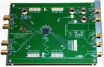
TLK2501 Serdes EVM Kit
Setup and Usage
User’s Guide
September 2000
Mixed Signal Products
SLLU010
�IMPORTANT NOTICE
Texas Instruments and its subsidiaries (TI) reserve the right to make changes to their products or to discontinue
any product or service without notice, and advise customers to obtain the latest version of relevant information
to verify, before placing orders, that information being relied on is current and complete. All products are sold
subject to the terms and conditions of sale supplied at the time of order acknowledgment, including those
pertaining to warranty, patent infringement, and limitation of liability.
TI warrants performance of its semiconductor products to the specifications applicable at the time of sale in
accordance with TI’s standard warranty. Testing and other quality control techniques are utilized to the extent
TI deems necessary to support this warranty. Specific testing of all parameters of each device is not necessarily
performed, except those mandated by government requirements.
Customers are responsible for their applications using TI components.
In order to minimize risks associated with the customer’s applications, adequate design and operating
safeguards must be provided by the customer to minimize inherent or procedural hazards.
TI assumes no liability for applications assistance or customer product design. TI does not warrant or represent
that any license, either express or implied, is granted under any patent right, copyright, mask work right, or other
intellectual property right of TI covering or relating to any combination, machine, or process in which such
semiconductor products or services might be or are used. TI’s publication of information regarding any third
party’s products or services does not constitute TI’s approval, warranty or endorsement thereof.
Copyright 2000, Texas Instruments Incorporated
�Notational Conventions
Preface
Read This First
About This Manual
This manual should be used to determine how to setup and use the TLK2501
evaluation module in order to evaluate the TLK2501 device.
How to Use This Manual
This document contains the following chapters:
-
Chapter 1 — Introduction
Chapter 2 — TLK2501 EVM Board Configuration
Chapter 3 — PCB Construction and Characteristics
Appendix A — Schematics, Board Layouts, and Suggested Optics and
Cable Assembly Specifications
Appendix B — NetLight 1417K4A 1300 nm Laser 2.5 Gbits/s
SpeedBlaster Transceiver data sheet
Notational Conventions
This document uses the following conventions.
-
Program listings, program examples, and interactive displays are shown
in a special typeface similar to a typewriter’s. Examples use a bold
version of the special typeface for emphasis; interactive displays use a
bold version of the special typeface to distinguish commands that you
enter from items that the system displays (such as prompts, command
output, error messages, etc.).
Here is a sample program listing:
0011
0012
0013
0014
0005
0005
0005
0006
0001
0003
0006
.field
.field
.field
.even
1, 2
3, 4
6, 3
Here is an example of a system prompt and a command that you might
enter:
C:
csr –a /user/ti/simuboard/utilities
Read This First
iii
�Trademarks
-
In syntax descriptions, the instruction, command, or directive is in a bold
typeface font and parameters are in an italic typeface. Portions of a syntax
that are in bold should be entered as shown; portions of a syntax that are
in italics describe the type of information that should be entered. Here is
an example of a directive syntax:
.asect ”section name”, address
.asect is the directive. This directive has two parameters, indicated by section name and address. When you use .asect, the first parameter must be
an actual section name, enclosed in double quotes; the second parameter
must be an address.
-
Square brackets ( [ and ] ) identify an optional parameter. If you use an
optional parameter, you specify the information within the brackets; you
don’t enter the brackets themselves. Here’s an example of an instruction
that has an optional parameter:
LALK 16–bit constant [, shift]
The LALK instruction has two parameters. The first parameter, 16-bit constant, is required. The second parameter, shift, is optional. As this syntax
shows, if you use the optional second parameter, you must precede it with
a comma.
Square brackets are also used as part of the pathname specification for
VMS pathnames; in this case, the brackets are actually part of the pathname (they are not optional).
-
Braces ( { and } ) indicate a list. The symbol | (read as or) separates items
within the list. Here’s an example of a list:
{ * | *+ | *– }
This provides three choices: *, *+, or *–.
Unless the list is enclosed in square brackets, you must choose one item
from the list.
-
Some directives can have a varying number of parameters. For example,
the .byte directive can have up to 100 parameters. The syntax for this directive is:
.byte value1 [, ... , valuen ]
This syntax shows that .byte must have at least one value parameter, but
you have the option of supplying additional value parameters, separated
by commas.
Trademarks
TI is a trademark of Texas Instruments.
NetLight and SpeedBlaster are trademarks of Lucent Technologies Inc.
iv
�Running Title—Attribute Reference
Contents
1
Introduction . . . . . . . . . . . . . . . . . . . . . . . . . . . . . . . . . . . . . . . . . . . . . . . . . . . . . . . . . . . . . . . . . . . . . 1-1
1.1
Introduction . . . . . . . . . . . . . . . . . . . . . . . . . . . . . . . . . . . . . . . . . . . . . . . . . . . . . . . . . . . . . . . . 1-2
1.2
TLK2501 EVM Kit Contents . . . . . . . . . . . . . . . . . . . . . . . . . . . . . . . . . . . . . . . . . . . . . . . . . . 1-2
2
TLK2501 EVM Board Configuration . . . . . . . . . . . . . . . . . . . . . . . . . . . . . . . . . . . . . . . . . . . . . . . 2-1
2.1
Typical Test and Setup Configurations . . . . . . . . . . . . . . . . . . . . . . . . . . . . . . . . . . . . . . . . . 2-3
2.2
Optical Interfacing and Configuration . . . . . . . . . . . . . . . . . . . . . . . . . . . . . . . . . . . . . . . . . . 2-7
3
PCB Construction and Characteristics . . . . . . . . . . . . . . . . . . . . . . . . . . . . . . . . . . . . . . . . . . . . 3-1
A
Schematics, Board Layouts, and Suggested Optics and Cable
Assembly Specifications . . . . . . . . . . . . . . . . . . . . . . . . . . . . . . . . . . . . . . . . . . . . . . . . . . . . . . . . . A-1
B
NetLight 1417K4A 1300 nm Laser 2.5 Gbits/s SpeedBlaster Transceiver . . . . . . . . . . B-1
Chapter Title—Attribute Reference
v
�Running Title—Attribute Reference
Figures
2–1
2–2
2–3
2–4
2–5
2–6
3–1
A–1
A–2
A–3
A–4
A–5
A–6
A–7
A–8
A–9
A–10.
A–11
A–12
A–13
A–14
A–15
A–16
A–17
vi
TLK2501 Serial Loop-Back Test Configuration . . . . . . . . . . . . . . . . . . . . . . . . . . . . . . . . . . . . 2-3
TLK2501 Serial Loop-Back Test Configuration . . . . . . . . . . . . . . . . . . . . . . . . . . . . . . . . . . . . 2-4
TLK2501 Serial PRBS BERT Test Configuration . . . . . . . . . . . . . . . . . . . . . . . . . . . . . . . . . . 2-5
TLK2501 Serial PRBS BERT Test Configuration . . . . . . . . . . . . . . . . . . . . . . . . . . . . . . . . . . 2-6
Optical Interface Configuration . . . . . . . . . . . . . . . . . . . . . . . . . . . . . . . . . . . . . . . . . . . . . . . . . . 2-7
TLK2501EVM to Laser Module Configuration . . . . . . . . . . . . . . . . . . . . . . . . . . . . . . . . . . . . . 2-8
TLK2501 EVM Layer Construction . . . . . . . . . . . . . . . . . . . . . . . . . . . . . . . . . . . . . . . . . . . . . . 3-3
TLK2501 EVM Transceiver Schematic . . . . . . . . . . . . . . . . . . . . . . . . . . . . . . . . . . . . . . . . . . . A-2
Optical Transceiver Schematic . . . . . . . . . . . . . . . . . . . . . . . . . . . . . . . . . . . . . . . . . . . . . . . . . . A-3
Top Layer 1 . . . . . . . . . . . . . . . . . . . . . . . . . . . . . . . . . . . . . . . . . . . . . . . . . . . . . . . . . . . . . . . . . . A-5
GND Layers 2 and 5 . . . . . . . . . . . . . . . . . . . . . . . . . . . . . . . . . . . . . . . . . . . . . . . . . . . . . . . . . . . A-6
Power Plane 1 . . . . . . . . . . . . . . . . . . . . . . . . . . . . . . . . . . . . . . . . . . . . . . . . . . . . . . . . . . . . . . . . A-7
Bottom Layer 6 . . . . . . . . . . . . . . . . . . . . . . . . . . . . . . . . . . . . . . . . . . . . . . . . . . . . . . . . . . . . . . . A-8
Bottom Layer 7 . . . . . . . . . . . . . . . . . . . . . . . . . . . . . . . . . . . . . . . . . . . . . . . . . . . . . . . . . . . . . . . A-9
Top Layer 1 . . . . . . . . . . . . . . . . . . . . . . . . . . . . . . . . . . . . . . . . . . . . . . . . . . . . . . . . . . . . . . . . . A-10
Detail of Top Layer 1 . . . . . . . . . . . . . . . . . . . . . . . . . . . . . . . . . . . . . . . . . . . . . . . . . . . . . . . . . A-11
GND Layers 2 and 5 . . . . . . . . . . . . . . . . . . . . . . . . . . . . . . . . . . . . . . . . . . . . . . . . . . . . . . . . . . A-12
Detail of GND Layers 2 and 5 . . . . . . . . . . . . . . . . . . . . . . . . . . . . . . . . . . . . . . . . . . . . . . . . . . A-13
Power Plane 1 . . . . . . . . . . . . . . . . . . . . . . . . . . . . . . . . . . . . . . . . . . . . . . . . . . . . . . . . . . . . . . . A-14
Detail of Power Plane 1 . . . . . . . . . . . . . . . . . . . . . . . . . . . . . . . . . . . . . . . . . . . . . . . . . . . . . . . A-15
Bottom Layer 6 . . . . . . . . . . . . . . . . . . . . . . . . . . . . . . . . . . . . . . . . . . . . . . . . . . . . . . . . . . . . . . A-16
Detail of Bottom Layer 6 . . . . . . . . . . . . . . . . . . . . . . . . . . . . . . . . . . . . . . . . . . . . . . . . . . . . . . A-17
Bottom Layer 6 . . . . . . . . . . . . . . . . . . . . . . . . . . . . . . . . . . . . . . . . . . . . . . . . . . . . . . . . . . . . . . A-18
Detail of Bottom Layer 6 . . . . . . . . . . . . . . . . . . . . . . . . . . . . . . . . . . . . . . . . . . . . . . . . . . . . . . A-19
�Running Title—Attribute Reference
Tables
2–1
2–2
3–1
3–2
A–1
Default Transceiver Board Configuration as Shipped . . . . . . . . . . . . . . . . . . . . . . . . . . . . . . .
Configuration Changes Necessary for DC-Coupling of the High Speed Signals . . . . . . . .
TLK2501 EVM TTL Bus PCB Transmission Line Characteristics . . . . . . . . . . . . . . . . . . . .
TLK2501 Differential Pair PCB Transmission Line Characteristics . . . . . . . . . . . . . . . . . . .
TLK2501 EVM Transceiver Bill of Materials . . . . . . . . . . . . . . . . . . . . . . . . . . . . . . . . . . . . . . .
Contents
2-2
2-2
3-2
3-2
A-4
vii
�viii
�Chapter 1
Introduction
The Texas Instruments (TI) TLK2501 serdes evaluation module (EVM) board
is used to evaluate the TLK2501 device(VQFP) and associated optical interface (NetLight) for point-to-point data transmission applications.
The board enables the designer to connect 50-Ω parallel buses to both
transmitter and receiver connectors. The TLK2501, using high speed PLL
technology, serializes, encodes (8b/10b) and transmits data along one
differential pair. The receiver part of the device deserializes, decodes, and
presents data on the parallel bus. The high speed (up to 2.5 Gbps) data lines
interface to four 50-Ω controlled-impedance SMA connectors. The designer
can either use this copper interface directly or loop back to the laser module
section for an optical interface(not provided).
Topic
1.1
Page
Introduction . . . . . . . . . . . . . . . . . . . . . . . . . . . . . . . . . . . . . . . . . . . . . . . . . . 1–2
1.2 TLK2501 EVM Kit Contents . . . . . . . . . . . . . . . . . . . . . . . . . . . . . . . . . . . . . . 1–2
Introduction
1-1
�Introduction
1.1 Introduction
The TLK2501 EVM board can be used to evaluate device parameters while
acting as a guide for high-speed board layout. The evaluation board can be
used as a daughter board that is plugged into new or existing designs. Since
the TLK2501 operates over a wide range of frequencies, designers need to
optimize designs for the frequency of interest. Additionally, designers may
wish to use buried transmission lines and provide additional noise attenuation
and EMI suppression to optimize their end product.
As the frequency of operation increases, the board designer must take special
care to ensure that the highest signal integrity is maintained. To achieve this,
the board’s impedance is controlled to 50 Ω for both the high-speed differential
serial and parallel data connections. In addition, impedance mismatches are
reduced by designing the component pad size to be as close as possible to
the width of the connecting transmission lines. Vias are minimized and, when
necessary, placed as close as possible to the device drivers. Since the board
contains both serial and parallel transmission lines, care was taken to control
both impedance and trace length mismatch (board skew).
Overall, the board layout is designed and optimized to support high-speed
operation. Thus, understanding impedance control and transmission line
effects are crucial when designing high-speed boards.
Some of the advanced features offered by this board include:
-
PCB (printed-circuit board) is designed for high-speed signal integrity.
Flexibility–The PCB can be configured for copper or optical interfaces.
SMA and parallel fixtures are easily connected to test equipment.
All input/output signals are accessible for rapid prototyping.
Analog and digital power planes can be supplied through separate banana
jacks for isolation or can be combined using ferrite bridging networks.
Series termination resistors provide parallel RD outputs.
Onboard capacitors provide ac coupling of high-speed signals.
1.2 TLK2501 EVM Kit Contents
-
1-2
TLK2501 EVM board
TLK2501 EVM kit documentation (This document)
�Chapter 2
TLK2501 EVM Board Configuration
The TLK2501 EVM board gives the developer various options for operation,
many of which are jumper selectable. Other options can be either soldered into
the EVM or connected through input connectors.
The TX and RX parallel connectors, J1–J4 of Figures 8 and 10 in Appendix A,
provide a connection for both transmitted and received data. The reference
clock is supplied through SMA connector J8, and jumper J5 must be installed
between pins 1 and 2. A direct clock connection can also be made to the J5
pins 1 and 3. The high-speed serial data is transmitted through J13 and J14
SMA connectors. The received recovered clock (RX_CLK) is output through
J15 header. Received data connects through SMA connectors J17 and J23 on
the RX side of the board. Header J7 provides static signals (normally pulled
high) to configure the device for different modes of operation. The J20 header
indicates the optical transmitter has detected a signal, and J21 allows the
operator to disable the optical transceiver.
The power planes are split three ways to provide power for different parts of
the board. This prevents coupling of switching noise between the analog and
digital sections of the TLK2501 and provides voltage isolation for the laser
section. The laser section of the board requires 3.3 volts and is energized
through the VCC connector. The VDD and VDDA connectors require 2.5 volts
and are joined together by a removable ferrite bead L3 that is installed in the
default configuration. Thus, only the VDD connection is necessary to energize
the TLK2501 device in the default configuration. In all sections of the board,
the ground planes are common and each ground plane is tied together at every
component ground connection. For detail schematic and layout see
TLK2501EVM Schematic, Optical Transceiver Schematic and Board Layer
Stack–up in Appendix A.
Topic
Page
2.1
Typical Test and Setup Configurations . . . . . . . . . . . . . . . . . . . . . . . . . . 2–3
2.2
Optical Interfacing and Configuration . . . . . . . . . . . . . . . . . . . . . . . . . . . 2–7
TLK2501 EVM Board Configuration
2-1
�The board is normally delivered in a default configuration that requires external
clock and data inputs. The TLK2501 is shipped with jumpers for default
operation. Table 2–1 shows the default configuration for sending data.
Table 2–1. Default Transceiver Board Configuration as Shipped
Designator
Function
J5
GTX CLK SEL
J7
TESTEN
Jumper installed (Logic 0)
Disables the TLK2501 test mode
J7
PRBSEN
Jumper installed (Logic 0)
Disables the TLK2501 PRBS internal production test mode
J7
LCKREFN
Jumper not installed (Logical 1)
Locks to received clock
J7
ENABLE
J7
TXER
J7
LOOPEN
J7
TXEN
L3
Condition
Jumper installed: J5 provides a method of supplying a input clock to
the board
Jumper not installed (Logical 1)
Enables the device for normal operation
Jumper installed (Logic 0)
Puts the TLK2501 in a state to transmit TX bus data.
Jumper installed (Logic 0)
Disables the TLK2501 internal loop back mode
Jumper not installed (Logical 1)
Puts the TLK2501 in a state to transmit TX bus data
VDD– bridge –VDDA Joins VDD and VDDA power planes
C24, C25
TX ac coupling
capacitors
These capacitors (normally installed) are provided to ac-couple the
transmitted signal.
C22, C23
RX ac coupling
capacitors
These capacitors (normally installed) are provided to ac-couple the
received signal
Note:
For details, see TLK2501 data sheet
Table 2–2. Configuration Changes Necessary for DC-Coupling of the High Speed Signals
Designator
Function
C24, C25
TX ac coupling
capacitors
Install zero ohm resistors
C22, C23
TX ac coupling
capacitors
Install zero ohm resistors.
R34
RX bias resistor
Install zero ohm resistor.
R33
RX bias resistor
Uninstall resistor (open circuit)
R37, R38
TX termination
network
Uninstall resistors (open circuit): Termination and pullup is achieved
at the receiver. Differential swing is increased.
2-2
Condition or Changes Necessary for DC Coupling
�Typical Test and Setup Configurations
2.1 Typical Test and Setup Configurations
The following configurations are used to evaluate and test the TLK2501
transceiver. The first configuration is a serial loopback of the high-speed
signals shown in Figure 2–1. The serial loopback allows the designer to
evaluate most of the functions of both transmitter and receiver sections of the
TLK2501 device. To test a system, a parallel bit error rate tester (BERT)
generates a predefined parallel bit pattern. The pattern is connected to the
transmitter through parallel connectors TD0–TD15. Additionally, two control
pins TX_ER and TX_EN are configured by the BERT for valid data
transmission (TX_ER low and TX_EN high). The TLK2501 device encodes,
serializes and presents the data on the high-speed serial pair. The serial TX
data is then looped back to the receiver side and the device deserializes,
decodes and presents the data on the receive side RD0–RD15. The data and
indication bits (RX_DV and RX_ER) are received by the BERT and compared
against the transmitted pattern and monitored for valid data and errors. If any
bit errors are received, a bit error rate is evaluated at the parallel receive BERT.
Figure 2–1. TLK2501 Serial Loop-Back Test Configuration
Jumper Selection
GND
HP8133A
Pulse Generator
TESTEN
PRBSEN
(Asynchronous to BERT)
LCKREFN
J7
EXT INPUT
ENABLE
Channel 1
O/P
TX_ER
LOOPEN
TX_EN
GND
Parallel BERT
Frequency = 80–125
MHz
GTX_CLK
CLK OUT
TX Data Out 0-17
18 bits
TX+
TX_EN
TX_ER
TX–
RX CLK
CLK IN
RX Data In 0-17
18 bits
Receiver BERT
TD 0-15
RX_ER
RX_DV
RX+
RD 0-15
RX–
TLK2501EVM
Evaluation Board
TLK2501 EVM Board Configuration
2-3
�Typical Test and Setup Configurations
If a parallel BERT is not available, the designer can take advantage of the built
in test mode of the device, see Figure 2–2. If the designer asserts the PRBSEN
pin high this results in a pseudo random bit pattern to be transmitted. This pin
also puts the receiver in a mode to detect a valid PRBS pattern. A valid pattern
is indicated by the PRBSPASS pin indicating high. This test only validates the
high-speed serial portion of the device and system interconnects. The PRBS
pattern is compatible with most serial BERT test equipment. This function
allows the operator to isolate and test the transmitter and receiver
independently. A typical configuration is shown in Figure 2–3. The dashed
lines represent optional connections that can be made monitoring eye patterns
and measuring jitter.
Figure 2–2. TLK2501 Serial Loop-Back Test Configuration
Jumper Selection
GND
TESTEN
HP83480 or
Tek 11801
HP8133A
Pulse Generator
PRBSEN
LCKREFN
J7
ENABLE
TX_ER
Digital
Oscilloscope
EXT
INPUT
TRIGGER
OUT
Channel 1
O/P
CH1
CH2
LOOPEN
TX_EN
GND
GTX_CLK
Channel 1
PRBS
2^7-1
TX–
TX+
TDS820 Digital
Oscilloscope
PRBS_PASS
RX+
RD 0-15
RX–
TLK2501EVM
Evaluation Board
2-4
PRBS 2^7-1
Trigger
�Typical Test and Setup Configurations
Figure 2–3. TLK2501 Serial PRBS BERT Test Configuration
Jumper Selection
GND
CLK/20
TESTEN
HP8133A
Pulse Generator
PRBSEN
LCKREFN
TX_ER
Digital
Oscilloscope
EXT
INPUT
J7
ENABLE
Channel 1
O/P
HP83480 or
Tek 11801
TRIGGER
OUT
CH1
CH2
LOOPEN
Trigger
TX_EN
GND
Serial BERT
HP7004A 3 Gbps
GTX_CLK
Channel 1
PRBS
2^7-1
Receiver BERT
Data In
TX–
TX+
Transmitter BERT
TDS820 Digital
Oscilloscope
PRBS_PASS
RX+
RD 0-15
RX–
Data Out
PRBS 2^7-1
Data Out
CLK OUT
TLK2501EVM
Evaluation Board
A board to board communication link is a practical method of evaluating the
TLK2501 in a system like environment as shown in Figure 2–4. A Parallel
BERT or a logic analyzer can be used to provide and monitor signals to and
from the transceiver pairs. The BERT would need to configure the TX_ER and
TX_EN signals for data transmission before any data is sent. On the receive
side the RX_ER and RX_DV can monitor the device for errors. Both GTX_CLK
sources must have the same frequency within 200 PPM for asynchronous
operation. Synchronous operation can be achieved by using either the BERT
or a synchronized pulse generator to supply both boards with GTX_CLK
inputs.
TLK2501 EVM Board Configuration
2-5
�Typical Test and Setup Configurations
Figure 2–4. TLK2501 Serial PRBS BERT Test Configuration
Jumper Selection
EVM #1
EVM #2
GND
GND
TESTEN
TESTEN
PRBSEN
PRBSEN
LCKREFN
LCKREFN
J7
ENABLE
HP8133A
Pulse Generator
J7
ENABLE
(Asynchronous to BERT)
TX_ER
TX_ER
LOOPEN
LOOPEN
TX_EN
TX_EN
GND
EXT INPUT
Trigger
Channel 1
O/P
GND
Asynchronous
Synchronous
GTX_CLK
GTX_CLK
16 bits
TD 0-15
TX+
RX+
RD 0-15
TX_EN
TX_ER
TX–
RX–
RX_ER
Rx_DV
RD 0-15
RX+
TX+
RX_CLK
RX–
TX–
TD 0-15
TLK2501EVM #1
Evaluation Board EVM1
PRBS Disabled
18 bits
Parallel BERT
Frequency = 80–125
MHz
TLK2501EVM #2
Evaluation Board EVM2
PRBS Disabled
Board configued to
send IDLE pattern:
TX_EN = 0
TX_ER = 0
TX Data Out 0-17
CLK Out
Transmitter BERT
CLK IN
RX Data In 0-17
18 bits
Receiver BERT
2-6
2 bits
Channel
1
�Optical Interfacing and Configuration
2.2 Optical Interfacing and Configuration
An interface between the TLK2501EVM and an optical transceiver can be
achieved in many ways depending on the design of the optics module and its
associated interface circuitry. Direct connection is achieved only if the optical
interface supports the current mode logic levels of the TLK2501 device (VDD
– 1 V). If the optics module does not support or can not be biased to the CML
levels, then ac-coupling must be used. Both ac- and dc- coupling schemes are
shown in Figure 2–5. The Laser Module Section of the EVM is configured as
an ac-coupled optics module. The board is shipped with an ac-coupled output
and all that is required is external loopback cabling.
Figure 2–5. Optical Interface Configuration
DC-Coupling
DC-Coupling
VDD
CMLDC bias levels
voltage ≈ (VDD-1 V)
TLK2501 TX
Optical Module
50 Ω
AC-Coupling
AC-Coupling
VDD
50 Ω
VCC
Biased to CML Levels
50 Ω
Optical Module
TLK2501 TX
50 Ω
Biased to PECL Levels
The Laser Module Section is isolated from the rest of the board and requires
external loopback as shown in Figure 2–6. This makes for a versatile system
where the laser can be connected independently to other EVM systems.
TLK2501 EVM Board Configuration
2-7
�Figure 2–6. TLK2501EVM to Laser Module Configuration
Optical Interfacing and Configuration
2-8
TLK2500 EVM Board Configuration
�Chapter 3
PCB Construction and Characteristics
The PCB characteristics are calculated and based on the layer construction
and trace width of the board. This should be useful in determining the proper
interface to the EVM and establishing system timing.
PCB Construction and Characteristics
3-1
�Table 3–1. TLK2501 EVM TTL Bus PCB Transmission Line Characteristics
Device
Pin No./Des.
Connector
Pin Label
Trace Width
(inches)
Length
(inches)
Capacitance
(pF)
Inductance
(nH)
Impedance
(Ω)
Line Delay
(ps)
62 – TXD0
TD0
0.0118
1.887
5.2
14.1
51.9
272.1
63 – TXD1
TD1
0.0118
1.884
5.2
14.1
51.9
271.7
64 – TXD2
TD2
0.0118
1.904
5.3
14.3
51.9
274.7
2 – TXD3
TD3
0.0118
1.898
5.3
14.2
51.9
273.7
3 – TXD4
TD4
0.0118
1.903
5.3
14.2
51.9
274.4
4 – TXD5
TD5
0.0118
1.899
5.3
14.2
51.9
273.8
6 – TXD6
TD6
0.0118
1.901
5.3
14.2
51.9
274.1
7 – TXD7
TD7
0.0118
1.906
5.3
14.3
51.9
274.8
10 – TXD8
TD8
0.0118
1.860
5.2
13.9
51.9
268.2
11 – TXD9
TD9
0.0118
1.908
5.3
14.3
51.9
275.1
12 – TXD10
TD10
0.0118
1.884
5.2
14.1
51.9
271.7
14 – TXD11
TD11
0.0118
1.912
5.3
14.3
51.9
275.7
15 – TXD12
TD12
0.0118
1.903
5.3
14.2
51.9
274.4
16 – TXD13
TD13
0.0118
1.910
5.3
14.3
51.9
275.4
17 – TXD14
TD14
0.0118
1.911
5.3
14.3
51.9
275.6
19 – TXD15
TD15
0.0118
1.901
5.3
14.2
51.9
274.1
51 – RXD0
RD0
0.0118
1.814
5.0
13.6
51.9
26.6
50 – RXD1
RD1
0.0118
1.804
5.0
13.5
51.9
260.3
49 – RXD2
RD2
0.0118
1.802
5.0
13.5
51.9
259.9
47 – RXD3
RD3
0.0118
1.862
5.2
13.9
51.9
268.5
46 – RXD4
RD4
0.0118
1.866
5.2
14.0
51.9
269.1
45 – RXD5
RD5
0.0118
1.876
5.2
14.0
51.9
270.5
44 – RXD6
RD6
0.0118
1.880
5.2
14.1
51.9
271.1
42 – RXD7
RD7
0.0118
1.865
5.2
14.0
51.9
268.9
40 – RXD8
RD8
0.0118
1.860
5.2
13.9
51.9
268.2
39 – RXD9
RD9
0.0118
1.860
5.2
13.9
51.9
268.2
37 – RXD10
RD10
0.0118
1.863
5.2
13.9
51.9
268.6
36 – RXD11
RD11
0.0118
1.872
5.2
14.0
51.9
269.9
35 – RXD12
RD12
0.0118
1.816
5.0
13.6
51.9
261.9
34 – RXD13
RD13
0.0118
1.855
5.2
13.9
51.9
267.5
32 – RXD14
RD14
0.0118
1.809
5.0
13.9
51.9
260.9
31 – RXD15
RD15
0.0118
1.821
5.1
13.6
51.9
262.9
Note:
All values presented in this table are theoretical calculated values and may not reflect actual measured parameters.
Table 3–2. TLK2501 Differential Pair PCB Transmission Line Characteristics
Device
Pin No.
Connector
Pin No.
Trace Width
(inches)
Length
(inches)
Impedance
(Ω)
Line Delay
(ps)
60 – DOUTTXP
TXP
0.025
2.390
51.2
347.5
59 – DOUTTXN
TXP
0.025
2.363
51.2
343.6
54 – DINRXP
RXP
0.025
2.889
51.2
420.1
53 – DINRXN
RXN
0.025
2.883
51.2
419.2
Note:
3-2
All values presented in this table are theoretical calculated values and may not reflect actual measured parameters.
�Figure 3–1. TLK2501 EVM Layer Construction
Top 50 Ω
Layer 1
14 Mil
GND1
Layer 2
5 Mil
Layer 3
VDD1
21 Mil
VDD2
Layer 4
05 Mil
Layer 5
GND2
07 Mil
Solder 50 Ω
Layer 6
Notes:
1) All cores consist of 1 oz. Cu.
2) Trace width
A) 25 mils (for 50 Ω Layer 1)
B) 11.8 mils (for 50 Ω Layer 6)
3) Overall board thickness is 62 mils ±5 mil
4) Copper and solder mask adds approximately 10 mils to the overall board thickness.
5) Impedance is 50 Ω ±5%
6) Material is G-Tek. Dielectric constant = 3.9
7) For overall thickness: add 1.2 to 1.4 mils for each metal layer in the stack-up.
PCB Construction and Characteristics
3-3
�3-4
�Appendix A
Schematics, Board Layouts, and Suggested
Optics and Cable Assembly Specifications
This appendix contains schematics and corresponding bill of materials for the
TLK2501EVM transceiver board along with board layouts. Specifications for
the NetLight 1417K4A 1300 nm laser assembly are also included.
Schematics, Board Layouts, and Suggested Optics and Cable Assembly Specifications
A-1
�Figure A–1. TLK2501 EVM Transceiver Schematic
VDD
GND
10u
J19
J22
C12
VDD
0.01
C6
0.01
C5
0.01
VDDA2
TXP
C4
TXN
0.01
0.01
VDDA1 RXP
0.01
C3
C38
J13
0.01
C39
J14
C2
VDDA2
C25 0.01
C32
0.01
C24
VDDA1
RXN
C40
J17
C22
100p
VDDA2
0.01
0.01
C41
J23
C23
0.01
R35
R36
49.9
49.9
0.01
100p
R38
C33
R37
C34
49.9
100p
100p
C26
49.9
0.01
0.01 C51
C35
VDD
100p
C21
C36
VDDA2
0.01
R33
100p
C37
825
10k 10k 10k 10k 10k 10k 10k 10k
R34
R41 200
J3
100
R25 R26 R27 R28 R29 R30 R31 R32
C19 0.01
J1
C20 0.01
2
3
4
5
6
7
8
9
10
12
11
13
VDDA1
51
VDDA1
1
R5
1
2
3
4
6
5
7
8
9
10
11
12
13
14
15
16
14
16
15
VDD
VDD
0.01
R4
C14
C18
0.01
VDD
open
51
R22
R3
R21
J15
VDD
0
49.9
1
J5
2
TLK2501
C15
0.01
VDD
R23
51
3
C17
0.01
R2
J8
R24
GTX_CLK
0
0.01
C42
VDD
51
J2
1
2
3
4
5
6
7
8
9
10
12
11
13
15
J4
51
VDD
0.01
14
16
R1
C16
VDD
2
R6
R7
R8
R13 R14 R15 R16 R17 R18 R19 R20
4
4.7k
J6
10k 10k 10k 10k 10k 10k 10k 10k
VDD
1
4.7k
R10
4.7k
R11
4.7k
R12
5
7
8
9
10
11
12
13
14
15
16
0.01
C10
C13
L1
L2
0.01
0.01
C9
C11
4.7k
2
4 6
4.7
8 10 12 14
C8
J16
J7
L3
3
5
7 1
9 11 13
0.01
VDDA
C7
0.01
VDD
A-2
4
6
0.01
3
4.7k
R9
2
3
VDDA2
VDDA1
4.7k
1
C1
�Figure A–2. Optical Transceiver Schematic
Schematics, Board Layouts, and Suggested Optics and Cable Assembly Specifications
A-3
�Table A–1.TLK2501 EVM Transceiver Bill of Materials
Item
Qty
Mfg / Dist.
Mfg Part No.
Ref Des
Description
Value or Function
1
1
Digi-Key
S2011–02–ND
J6
2×2 header
0.1 x 0.1 centers
2
1
Digi-Key
S2011–07–ND
J7
2×7 header
0.1 x 0.1 centers
3
4
Digi-Key
ECS–T1DX475R
J1, J2, J3, J4
2×8 header
0.1 x 0.1 centers
4
1
Digi-Key
S1111–03–ND
J5
3 Pin jumper
0.1 CENTERS
5
4
Newark
39N867
J16,J18,J19,
J22
Banana jack
100 V, 5%, 0.1 µF
6
40
Digi-Key
PCC1784CT–ND
C1–C7,
C9–C11,
C13–C26, C29,
C31, C38–C51
Capacitor, SMT603
25 V, 5%, 0.01 µF
7
4
Digi-Key
PCC1842CT–ND
C8,C27,
C28,C30
Capacitor, SMT0603
25 V, 5%, 4.7 µF
8
1
Digi-Key
PCC1894CT–ND
C12
Capacitor, SMT0805
25 V, 5%, 10 µF
10
2
Digi-Key
S1111–02–ND
J15, J20
Jumper
Header, 1×2,
0.1 center
11
1
LUCENT
1417K4A LAS
U2
Laser transceiver
2.5 Gbps
12
2
Digi-Key
TSW–110–07–G–D
R21, R24
Resistor, SMT, 0402
0Ω
13
7
Any
P4.75KLTC–ND
R6–R12
Resistor, SMT, 0402
4.7 kΩ
14
16
Digi-Key
P10.0KLTC–ND
R15–R20,
R25–R32
Resistor, SMT, 0402
10 kΩ
15
5
Digi-Key
P49.9LCT–ND
R23, R35, R36,
R37, R38
Resistor, SMT, 0402
49.9 Ω
16
2
Digi-Key
P130LTC–ND
R39, R40
Resistor, SMT, 0402
130 Ω
17
2
Digi-Key
P200LTC–ND
R34, R41
Resistor, SMT, 0402
200 Ω
18
1
Digi-Key
P825LTC–ND
R33
Resistor, SMT, 0402
825 Ω
19
1
N/A
N/A
R22
Resistor, SMT, 0402
OPEN
20
5
MNR14 E0AB J 510
R1, R2, R3, R4,
R5
Resistor R–PAC(4)
51 Ω
21
9
Newark
142–0711–821
SMA end–launch
422 Ω
22
4
Newark
92N4922
23
4
Newark
30F082
24
1
TI
TLK2501
U1
TI TLK2501 DUT
64 PIN VQFP
25
6
Digi-Key
PCC101ACVCT–ND
C32–C37
Capacitor, SMT 0603
25 V, 20%, 100 pF
26
3
Digi-Key
240–1018–1ND
L1–L3
Ferrite bead
805 500 ma
600 Ω
A-4
STANDOFF
Standoff 0.5’ 4–40 thread
Machine screw 4–40 × 3/8’
�Figure A–3. Top Layer 1
Schematics, Board Layouts, and Suggested Optics and Cable Assembly Specifications
A-5
�Figure A–4. GND Layers 2 and 5
A-6
�Figure A–5. Power Plane 1
Schematics, Board Layouts, and Suggested Optics and Cable Assembly Specifications
A-7
�Figure A–6. Bottom Layer 6
A-8
�Figure A–7. Bottom Layer 7
Schematics, Board Layouts, and Suggested Optics and Cable Assembly Specifications
A-9
�Figure A–8. Top Layer 1
A-10
Schematics, Board Layouts, and Suggested Optics and Cable Assembly Specifications
�R1
R22
open
R5
R4
Pin 1
0
R21
R23
R24
0
R2
R3
Figure A–9. Detail of Top Layer 1
Schematics, Board Layouts, and Suggested Optics and Cable Assembly Specifications
A-11
�Figure A–10. GND Layers 2 and 5
A-12
Schematics, Board Layouts, and Suggested Optics and Cable Assembly Specifications
�Figure A–11. Detail of GND Layers 2 and 5
Schematics, Board Layouts, and Suggested Optics and Cable Assembly Specifications
A-13
�Figure A–12. Power Plane 1
A-14
Schematics, Board Layouts, and Suggested Optics and Cable Assembly Specifications
�Figure A–13. Detail of Power Plane 1
Schematics, Board Layouts, and Suggested Optics and Cable Assembly Specifications
A-15
�Figure A–14. Bottom Layer 6
A-16
Schematics, Board Layouts, and Suggested Optics and Cable Assembly Specifications
�Figure A–15. Detail of Bottom Layer 6
Schematics, Board Layouts, and Suggested Optics and Cable Assembly Specifications
A-17
�Figure A–16. Bottom Layer 6
A-18
Schematics, Board Layouts, and Suggested Optics and Cable Assembly Specifications
�Figure A–17. Detail of Bottom Layer 6
Schematics, Board Layouts, and Suggested Optics and Cable Assembly Specifications
A-19
�A-20
Schematics, Board Layouts, and Suggested Optics and Cable Assembly Specifications
�Appendix B
NetLight 1417K4A 1300 nm Laser 2.5 Gbits/s
SpeedBlaster Transceiver
The document shown in this appendix is an advanced information data sheet
from Lucent Technologies Inc.
Topic
Page
NetLight 1417K4A 1300 nm Laser 2.5 Gbits/s Speedmaster
Transceiver Data Sheet . . . . . . . . . . . . . . . . . . . . . . . . . . . . . . . . . . . . . . . B–2
Lucent, NetLight, and Speedmaster are a trademarks of Lucent Technologies Inc.
NetLight 1417K4A 1300 nm Laser 2.5 Gbits/s SpeedBlaster Transceiver
B-1
�B-2
�NetLight 1417K4A 1300 nm Laser 2.5 Gbits/s SpeedBlaster Transceiver
B-3
�B-4
�NetLight 1417K4A 1300 nm Laser 2.5 Gbits/s SpeedBlaster Transceiver
B-5
�B-6
�NetLight 1417K4A 1300 nm Laser 2.5 Gbits/s SpeedBlaster Transceiver
B-7
�B-8
�NetLight 1417K4A 1300 nm Laser 2.5 Gbits/s SpeedBlaster Transceiver
B-9
�B-10
�NetLight 1417K4A 1300 nm Laser 2.5 Gbits/s SpeedBlaster Transceiver
B-11
�B-12
�