Product
Folder
Sample &
Buy
Technical
Documents
Support &
Community
Tools &
Software
TLV1117
SLVS561L – DECEMBER 2004 – REVISED OCTOBER 2014
TLV1117 Adjustable and Fixed Low-Dropout Voltage Regulator
1 Features
3 Description
•
The TLV1117 device is a positive low-dropout voltage
regulator designed to provide up to 800 mA of output
current. The device is available in 1.5-V, 1.8-V, 2.5-V,
3.3-V, 5-V, and adjustable-output voltage options. All
internal circuitry is designed to operate down to 1-V
input-to-output differential. Dropout voltage is
specified at a maximum of 1.3 V at 800 mA,
decreasing at lower load currents.
1
•
•
•
•
1.5-V, 1.8-V, 2.5-V, 3.3-V, 5-V, and
Adjustable-Output Voltage Options
Output Current of 800 mA
Specified Dropout Voltage at Multiple
Current Levels
0.2% Line Regulation Maximum
0.4% Load Regulation Maximum
Device Information
2 Applications
•
•
•
•
•
ORDER NUMBER
Electronic Points of Sale
Medical, Health, and Fitness Applications
Printers
Appliances and White Goods
TV Set-Top Boxes
PACKAGE (PIN)
BODY SIZE
TLV1117DCY
SOT-223 (4)
6.50 mm × 3.50 mm
TLV1117DRJ
SON (8)
4.00 mm × 4.00 mm
TLV1117KVU
TO-252 (3)
6.60 mm × 6.10 mm
TLV1117KCS
TO-220 (3)
10.16 mm × 8.70 mm
TLV1117KCT
TO-220 (3)
10.16 mm × 8.59 mm
TLV1117KTT
DDPAK,
TO-263 (3)
10.18 mm × 8.41 mm
4 Simplified Schematic
TLV1117-ADJ
INPUT
OUTPUT
ADJ/GND
1
An IMPORTANT NOTICE at the end of this data sheet addresses availability, warranty, changes, use in safety-critical applications,
intellectual property matters and other important disclaimers. PRODUCTION DATA.
�TLV1117
SLVS561L – DECEMBER 2004 – REVISED OCTOBER 2014
www.ti.com
Table of Contents
1
2
3
4
5
6
7
8
Features ..................................................................
Applications ...........................................................
Description .............................................................
Simplified Schematic.............................................
Revision History.....................................................
Pin Configuration and Functions .........................
Specifications.........................................................
1
1
1
1
2
3
4
7.1
7.2
7.3
7.4
7.5
7.6
7.7
4
4
4
5
6
7
8
Absolute Maximum Ratings .....................................
Handling Ratings ......................................................
Recommended Operating Conditions.......................
Thermal Information ..................................................
TLV1117C Electrical Characteristics ........................
TLV1117I Electrical Characteristics ..........................
Typical Characteristics ..............................................
Detailed Description ............................................ 10
8.1
8.2
8.3
8.4
9
Overview .................................................................
Functional Block Diagram .......................................
Feature Description.................................................
Device Functional Modes........................................
10
10
10
10
Application and Implementation ........................ 12
9.1 Typical Application ................................................. 12
10 Power Supply Recommendations ..................... 13
11 Layout................................................................... 13
11.1 Layout Guidelines ................................................. 13
11.2 Layout Example .................................................... 13
12 Device and Documentation Support ................. 14
12.1 Trademarks ........................................................... 14
12.2 Electrostatic Discharge Caution ............................ 14
12.3 Glossary ................................................................ 14
13 Mechanical, Packaging, and Orderable
Information ........................................................... 14
Changes from Revision K (April 2013) to Revision L
Page
•
Updated data sheet to new TI standards – no specification changes. .................................................................................. 1
•
Deleted Ordering Information table. ...................................................................................................................................... 1
•
Added Applications. ................................................................................................................................................................ 1
•
Added Device and Documentation Support section............................................................................................................. 14
•
Added Mechanical, Packaging, and Orderable Information section..................................................................................... 14
5 Revision History
Changes from Revision J (April 2013) to Revision K
Page
•
Added additional package options.......................................................................................................................................... 3
•
Added ESD warning. ............................................................................................................................................................ 14
2
Submit Documentation Feedback
Copyright © 2004–2014, Texas Instruments Incorporated
Product Folder Links: TLV1117
�TLV1117
www.ti.com
SLVS561L – DECEMBER 2004 – REVISED OCTOBER 2014
6 Pin Configuration and Functions
KVU (TO-252) PACKAGE
(TOP VIEW)
INPUT
2
OUTPUT
1
ADJ/GND
DCY (SOT-223) PACKAGE
(TOP VIEW)
OUTPUT
3
2
ADJ/GND
1
VIN(1)
2
(1)
VIN(1)
OUTPUT
VIN
1
ADJ/GND
8
NC
7
VOUT(2)
3
6
VOUT(2)
4
5
VOUT(2)
VOUT
INPUT
2
OUTPUT
1
ADJ/GND
KCT, KCS (TO-220) PACKAGE
(TOP VIEW)
DRJ (QFN) PACKAGE
(TOP VIEW)
INPUT
3
OUTPUT
3
OUTPUT
OUTPUT
KTT (TO-263) PACKAGE
(TOP VIEW)
3
2
1
INPUT
OUTPUT
ADJ/GND
(1) VIN pins (2, 3, 4) must be connected together.
(2) VOUT pins (5, 6, 7) must be connected together.
Table 1. Pin Functions
PIN
NAME
KTT
KVU DCY
DRJ
KCT
TYPE
DESCRIPTION
ADJ/GND
1
1
1
1
1
I/O
INPUT
3
3
3
2, 3, 4
3
I
Output voltage adjustment pin. Connect to a resistor divider.
Voltage input
OUTPUT
2
2
2
5, 6, 7
2
O
Voltage output
NC
-
-
-
8
-
-
No connect
Submit Documentation Feedback
Copyright © 2004–2014, Texas Instruments Incorporated
Product Folder Links: TLV1117
3
�TLV1117
SLVS561L – DECEMBER 2004 – REVISED OCTOBER 2014
www.ti.com
7 Specifications
7.1 Absolute Maximum Ratings (1)
over operating free-air temperature range (unless otherwise noted)
MIN
VIN
Continuous input voltage
TJ
Operating virtual-junction temperature
(1)
MAX
UNIT
16
V
150
°C
Stresses beyond those listed under Absolute Maximum Ratings may cause permanent damage to the device. These are stress ratings
only, and functional operation of the device at these or any other conditions beyond those indicated under Recommended Operating
Conditions is not implied. Exposure to absolute-maximum-rated conditions for extended periods may affect device reliability.
7.2 Handling Ratings
Tstg
Storage temperature range
V(ESD)
(1)
(2)
Electrostatic discharge
MIN
MAX
UNIT
°C
–65
150
Human body model (HBM), per ANSI/ESDA/JEDEC JS-001, all
pins (1)
0
2500
Charged device model (CDM), per JEDEC specification
JESD22-C101, all pins (2)
0
1500
V
JEDEC document JEP155 states that 500-V HBM allows safe manufacturing with a standard ESD control process.
JEDEC document JEP157 states that 250-V CDM allows safe manufacturing with a standard ESD control process.
7.3 Recommended Operating Conditions
VIN
Input voltage
IO
Output current
TJ
Operating virtual-junction temperature
(1)
4
MIN (1)
MAX
TLV1117
2.7
15
TLV1117-15
2.9
15
TLV1117-18
3.2
15
TLV1117-25
3.9
15
TLV1117-33
4.7
15
TLV1117-50
6.4
TLV1117I
V
15
0.8
TLV1117C
UNIT
0
125
–40
125
A
°C
The input-to-output differential across the regulator should provide for some margin against regulator operation at the maximum dropout
(for a particular current value). This margin is needed to account for tolerances in both the input voltage (lower limit) and the output
voltage (upper limit). The absolute minimum VIN for a desired maximum output current can be calculated by the following:
VIN(min) = VOUT(max) + VDO(max at rated current)
Submit Documentation Feedback
Copyright © 2004–2014, Texas Instruments Incorporated
Product Folder Links: TLV1117
�TLV1117
www.ti.com
SLVS561L – DECEMBER 2004 – REVISED OCTOBER 2014
7.4 Thermal Information
TLV1117
THERMAL METRIC (1) (2) (3)
PowerFlex
UNITS
KTE
(3 PINS)
KTP
(3 PINS)
DRJ
(8 PINS)
DCY
(4 PINS)
KVU
(3 PINS)
KCS, KCT
(3 PINS)
KTT
(3 PINS)
RθJA
Junction-to-ambient thermal
resistance
38.6
49.2
38.3
104.3
50.9
30.1
27.5
RθJC(top)
Junction-to-case (top) thermal
resistance
34.7
60.6
36.5
53.7
57.9
44.6
43.2
RθJB
Junction-to-board thermal resistance
3.2
3.1
60.5
5.7
34.8
1.2
17.3
ψJT
Junction-to-top characterization
parameter
5.9
8.7
0.2
3.1
6
5
2.8
ψJB
Junction-to-board characterization
parameter
3.1
3
12
5.5
23.7
1.2
9.3
RθJC(bot)
Junction-to-case (bottom) thermal
resistance
3
3
4.7
n/a
0.4
0.4
0.3
RθJP
Thermal resistance between the die
junction and the bottom of the
exposed pad.
2.7
1.4
1.78
n/a
n/a
3
1.94
(1)
(2)
(3)
°C/W
For more information about traditional and new thermal metrics, see the IC Package Thermal Metrics application report, SPRA953.
For thermal estimates of this device based on PCB copper area, see the TI PCB Thermal Calculator.
Maximum power dissipation is a function of TJ(max), θJA, and TA. The maximum allowable power dissipation at any allowable ambient
temperature is PD = (TJ(max) – TA) / θJA. Operating at the absolute maximum TJ of 150°C can affect reliability.
Submit Documentation Feedback
Copyright © 2004–2014, Texas Instruments Incorporated
Product Folder Links: TLV1117
5
�TLV1117
SLVS561L – DECEMBER 2004 – REVISED OCTOBER 2014
www.ti.com
7.5 TLV1117C Electrical Characteristics
TJ = 0°C to 125°C, all typical values are at TJ = 25°C (unless otherwise noted)
TEST CONDITIONS (1)
PARAMETER
Reference voltage, VREF
VIN – VOUT = 2 V, IOUT = 10 mA, TJ = 25°C
VIN – VOUT = 1.4 V to 10 V, IOUT = 10 mA to 800 mA
VIN = 3.5 V, IOUT = 10 mA, TJ = 25°C
VIN = 2.9 V to 10 V, IOUT = 0 to 800 mA
VIN = 3.8 V, IOUT = 10 mA, TJ = 25°C
VIN = 3.2 V to 10 V, IOUT = 0 to 800 mA
VIN = 4.5 V, IOUT = 10 mA, TJ = 25°C
Output voltage, VOUT
VIN = 3.9 V to 10 V, IOUT = 0 to 800 mA
VIN = 5 V, IOUT = 10 mA, TJ = 25°C
VIN = 4.75 V to 10 V, IOUT = 0 to 800 mA
VIN = 7 V, IOUT = 10 mA, TJ = 25°C
VIN = 6.5 V to 12 V, IOUT = 0 to 800 mA
Line regulation
Load regulation
Dropout voltage, VDO
(2)
TLV1117
TLV1117-15
TLV1117-18
TLV1117-25
TLV1117-33
TLV1117-50
MIN
TYP
MAX
1.238
1.25
1.262
1.225
1.25
1.27
1.485
1.5
1.515
1.455
1.5
1.545
1.782
1.8
1.818
1.746
1.8
1.854
2.475
2.5
2.525
2.450
2.5
2.550
3.267
3.3
3.333
3.235
3.3
3.365
4.950
5.0
5.050
4.900
5.0
5.100
0.035%
0.2%
IOUT = 10 mA, VIN – VOUT = 1.5 V to 13.75 V
TLV1117
IOUT = 0 mA, VIN = 2.9 V to 10 V
TLV1117-15
1
6
IOUT = 0 mA, VIN = 3.2 V to 10 V
TLV1117-18
1
6
IOUT = 0 mA, VIN = 3.9 V to 10 V
TLV1117-25
1
6
IOUT = 0 mA, VIN = 4.75 V to 15 V
TLV1117-33
1
6
IOUT = 0 mA, VIN = 6.5 V to 15 V
TLV1117-50
IOUT = 10 mA to 800 mA, VIN – VOUT = 3 V
TLV1117
IOUT = 0 to 800 mA, VIN = 2.9 V
1
10
0.2%
0.4%
TLV1117-15
1
10
IOUT = 0 to 800 mA, VIN = 3.2 V
TLV1117-18
1
10
IOUT = 0 to 800 mA, VIN = 3.9 V
TLV1117-25
1
10
IOUT = 0 to 800 mA, VIN = 4.75 V
TLV1117-33
1
10
IOUT = 0 to 800 mA, VIN = 6.5 V
TLV1117-50
1
15
UNIT
V
—
mV
—
mV
IOUT = 100 mA
1.1
1.2
IOUT = 500 mA
1.15
1.25
IOUT = 800 mA
1.2
1.3
1.2
1.6
1.7
5
mA
5
10
mA
0.01
0.1
%/W
80
120
μA
0.2
5
μA
Current limit
VIN – VOUT = 5 V, TJ = 25°C (3)
Minimum load current
VIN = 15 V
TLV1117
Quiescent current
VIN ≤ 15 V
All fixed-voltage
options
Thermal regulation
30-ms pulse, TA = 25°C
Ripple rejection
VIN – VOUT = 3 V, Vripple = 1 Vpp, f = 120 Hz
ADJ pin current
0.8
60
75
V
A
dB
Change in ADJ pin current
VIN – VOUT = 1.4 V to 10 V, IOUT = 10 mA to 800 mA
Temperature stability
TJ = full range
0.5%
—
Long-term stability
1000 hrs, No load, TA = 125°C
0.3%
—
Output noise voltage
(% of VOUT)
f = 10 Hz to 100 kHz
0.003%
—
(1)
(2)
(3)
6
All characteristics are measured with a 10-μF capacitor across the input and a 10-μF capacitor across the output. Pulse testing
techniques are used to maintain the junction temperature as close to the ambient temperature as possible.
Dropout is defined as the VIN to VOUT differential at which VOUT drops 100 mV below the value of VOUT,
measured at VIN = VOUT(nom) + 1.5 V.
Current limit test specified under recommended operating conditions.
Submit Documentation Feedback
Copyright © 2004–2014, Texas Instruments Incorporated
Product Folder Links: TLV1117
�TLV1117
www.ti.com
SLVS561L – DECEMBER 2004 – REVISED OCTOBER 2014
7.6 TLV1117I Electrical Characteristics
TJ = –40°C to 125°C, all typical values are at TJ = 25°C (unless otherwise noted)
TEST CONDITIONS (1)
PARAMETER
Reference voltage, VREF
VIN – VOUT = 2 V, IOUT = 10 mA, TJ = 25°C
VIN – VOUT = 1.4 V to 10 V, IOUT = 10 mA to 800 mA
VIN = 3.5 V, IOUT = 10 mA, TJ = 25°C
VIN = 2.9 V to 10 V, IOUT = 0 to 800 mA
VIN = 3.8 V, IOUT = 10 mA, TJ = 25°C
VIN = 3.2 V to 10 V, IOUT = 0 to 800 mA
VIN = 4.5 V, IOUT = 10 mA, TJ = 25°C
Output voltage, VOUT
VIN = 3.9 V to 10 V, IOUT = 0 to 800 mA
VIN = 5 V, IOUT = 10 mA, TJ = 25°C
VIN = 4.75 V to 10 V, IOUT = 0 to 800 mA
VIN = 7 V, IOUT = 10 mA, TJ = 25°C
VIN = 6.5 V to 12 V, IOUT = 0 to 800 mA
Line regulation
Load regulation
Dropout voltage, VDO
(2)
TLV1117
TLV1117-15
TLV1117-18
TLV1117-25
TLV1117-33
TLV1117-50
MIN
TYP
MAX
1.238
1.25
1.262
1.200
1.25
1.29
1.485
1.5
1.515
1.44
1.5
1.56
1.782
1.8
1.818
1.728
1.8
1.872
2.475
2.5
2.525
2.4
2.5
2.6
3.267
3.3
3.333
3.168
3.3
3.432
4.95
5.0
5.05
4.80
5.0
5.20
0.035%
0.3%
IOUT = 10 mA, VIN – VOUT = 1.5 V to 13.75 V
TLV1117
IOUT = 0 mA, VIN = 2.9 V to 10 V
TLV1117-15
1
10
IOUT = 0 mA, VIN = 3.2 V to 10 V
TLV1117-18
1
10
IOUT = 0 mA, VIN = 3.9 V to 10 V
TLV1117-25
1
10
IOUT = 0 mA, VIN = 4.75 V to 15 V
TLV1117-33
1
10
IOUT = 0 mA, VIN = 6.5 V to 15 V
TLV1117-50
IOUT = 10 mA to 800 mA, VIN – VOUT = 3 V
TLV1117
IOUT = 0 to 800 mA, VIN = 2.9 V
1
15
0.2%
0.5%
TLV1117-15
1
15
IOUT = 0 to 800 mA, VIN = 3.2 V
TLV1117-18
1
15
IOUT = 0 to 800 mA, VIN = 3.9 V
TLV1117-25
1
15
IOUT = 0 to 800 mA, VIN = 4.75 V
TLV1117-33
1
15
IOUT = 0 to 800 mA, VIN = 6.5 V
TLV1117-50
1
20
UNIT
V
—
mV
—
mV
IOUT = 100 mA
1.1
1.3
IOUT = 500 mA
1.15
1.35
IOUT = 800 mA
1.2
1.4
1.2
1.6
1.7
5
mA
5
15
mA
0.01
0.1
%/W
80
120
μA
0.2
10
μA
Current limit
VIN – VOUT = 5 V, TJ = 25°C (3)
Minimum load current
VIN = 15 V
TLV1117
Quiescent current
VIN ≤ 15 V
All fixed-voltage
options
Thermal regulation
30-ms pulse, TA = 25°C
Ripple rejection
VIN – VOUT = 3 V, Vripple = 1 Vpp, f = 120 Hz
0.8
ADJ pin current
60
75
V
A
dB
Change in ADJ pin current
VIN – VOUT = 1.4 V to 10 V, IOUT = 10 mA to 800 mA
Temperature stability
TJ = full range
0.5%
—
Long-term stability
1000 hrs, No load, TA = 125°C
0.3%
—
Output noise voltage
(% of VOUT)
f = 10 Hz to 100 kHz
0.003%
—
(1)
(2)
(3)
All characteristics are measured with a 10-μF capacitor across the input and a 10-μF capacitor across the output. Pulse testing
techniques are used to maintain the junction temperature as close to the ambient temperature as possible.
Dropout is defined as the VIN to VOUT differential at which VOUT drops 100 mV below the value of VOUT,
measured at VIN = VOUT(nom) + 1.5 V.
Current limit test specified under recommended operating conditions
Submit Documentation Feedback
Copyright © 2004–2014, Texas Instruments Incorporated
Product Folder Links: TLV1117
7
�TLV1117
SLVS561L – DECEMBER 2004 – REVISED OCTOBER 2014
www.ti.com
7.7 Typical Characteristics
0
1.8
TJ = 255C
DLoad = 800 mA
1.6
−0.05
Short-Circuit Current (A)
1.4
TJ = 1255C
−0.1
DVOUT (%)
1.2
1
0.8
−0.15
−0.2
0.6
−0.25
0.4
−0.3
0.2
0
0
3
6
9
12
−0.35
−50
15
−25
0
Input/Output Differential (V)
Figure 1. Short-Circuit Current vs (VIN – VOUT)
90
70
80
100
125
f = 120 Hz
Ripple Rejection (dB)
Ripple Rejection (dB)
75
70
50
40
30
20
60
50
40
30
20
10
10
0
0
10
100
1k
10k
100k
0
200
Frequency (Hz)
600
800
Figure 4. Ripple Rejection vs Load Current (ADJ Version)
2
150
1.5
140
130
ADJ Pin Current (mA)
1
0.5
0
−0.5
−1
120
110
100
90
80
−1.5
−2
−50
400
Load (mA)
Figure 3. Ripple Rejection vs Frequency (ADJ Version)
Output Voltage Variation (%)
50
Figure 2. Load Regulation
80
60
8
25
Temperature (5C)
70
−25
0
25
50
75
100
125
150
60
−50
−25
0
25
50
75
100
125
150
Temperature (5C)
Temperature (5C)
Figure 5. Temperature Stability
Figure 6. ADJ Pin Current vs Temperature
Submit Documentation Feedback
Copyright © 2004–2014, Texas Instruments Incorporated
Product Folder Links: TLV1117
�TLV1117
www.ti.com
SLVS561L – DECEMBER 2004 – REVISED OCTOBER 2014
Typical Characteristics (continued)
100
2.4
90
2.2
Output-Voltage Deviation
1.6
1.4
−0.1
CIN = 10 mF
COUT = 10-mF Tantalum
−0.2 VIN = 4.8 V
Preload = 0.1 A
1.2
1
0.8
0.6
−0.3
0.4
Load Current
0.2
−0.4
−0.5
−60
Load Current (A)
1.8
0
−40
−20
0
7
Input Voltage
6
80
2
Output Voltage Deviation (mV)
0.1
Output Voltage Deviation (V)
2.6
70
5
60
50
40
30
CIN = 0.1 mF
COUT = 10-mF Tantalum
IOUT = 0.1 A
3
20
Output-Voltage Deviation
10
2
0
0
−10
−0.2
−20
−40 −20
20
4
Input Voltage (V)
0.2
Time (ms)
1
0
20
40
60
80 100 120 140
Time (ms)
Figure 7. TLV1117-33 Load Transient Response
Figure 8. TLV1117-33 Line Transient Response
Submit Documentation Feedback
Copyright © 2004–2014, Texas Instruments Incorporated
Product Folder Links: TLV1117
9
�TLV1117
SLVS561L – DECEMBER 2004 – REVISED OCTOBER 2014
www.ti.com
8 Detailed Description
8.1 Overview
The TLV1117 device is a positive low-dropout voltage regulator designed to provide up to 800 mA of output
current. The device is available in 1.5-V, 1.8-V, 2.5-V, 3.3-V, 5-V, and adjustable-output voltage options. All
internal circuitry is designed to operate down to 1-V input-to-output differential. Dropout voltage is specified at a
maximum of 1.3 V at 800 mA, decreasing at lower load currents.
The TLV1117 device is designed to be stable with tantalum and aluminum electrolytic output capacitors having
an ESR between 0.2 Ω and 10 Ω.
Unlike pnp-type regulators, in which up to 10% of the output current is wasted as quiescent current, the
quiescent current of the TLV1117 device flows into the load, increasing efficiency.
The TLV1117C device is characterized for operation over the virtual junction temperature range of 0°C to 125°C,
and the TLV1117I device is characterized for operation over the virtual junction temperature range of –40°C to
125°C.
8.2 Functional Block Diagram
Functional Block Diagram
80 !A
+
1.25 V
Overload
Block
INPUT
5 mA
OUTPUT
ADJUST
8.3 Feature Description
8.3.1 NPN Output Drive
NPN output topology provides lower output impedance than most LDOs. However, an output capacitor is
required. To support maximum current and lowest temperature, 1.4-V headroom is recommended (less for lower
currents) (VI – VO).
8.3.2 Overload Block
Current limiting and over temperature shutdown protects against overload or under heat sinking.
8.3.3 Programmable Feedback
Op amp with 1.25-V offset input at the ADJUST pin provides easy output voltage programming. For current
regulation applications, a single resistor whose resistance value is 1.25 V / IOUT and power rating is greater than
(1.25 V)2 / R should be used. For voltage regulation applications, two resistors set the output voltage.
8.4 Device Functional Modes
8.4.1 Normal operation
The device OUTPUT pin will source current necessary to make OUTPUT pin 1.25 V greater than ADJUST
terminal to provide output regulation.
10
Submit Documentation Feedback
Copyright © 2004–2014, Texas Instruments Incorporated
Product Folder Links: TLV1117
�TLV1117
www.ti.com
SLVS561L – DECEMBER 2004 – REVISED OCTOBER 2014
Device Functional Modes (continued)
8.4.2 Operation With Low Input Voltage
The adjustable version of the device requires 1-V headroom (VI – VO) to operate in regulation. With less
headroom, the device may drop out and OUTPUT voltage will be INPUT voltage minus drop out voltage.
8.4.3 Operation at Light Loads
The device passes its bias current to the OUTPUT pin. The load or feedback must consume this minimum
current for regulation or the output may be too high.
8.4.4 Operation in Self Protection
When an overload occurs the device will shut down the output stage or reduce the output current to prevent
device damage. The device will automatically reset from the overload. The output may be reduced or alternate
between on and off until the overload is removed.
Submit Documentation Feedback
Copyright © 2004–2014, Texas Instruments Incorporated
Product Folder Links: TLV1117
11
�TLV1117
SLVS561L – DECEMBER 2004 – REVISED OCTOBER 2014
www.ti.com
9 Application and Implementation
NOTE
Information in the following applications sections is not part of the TI component
specification, and TI does not warrant its accuracy or completeness. TI’s customers are
responsible for determining suitability of components for their purposes. Customers should
validate and test their design implementation to confirm system functionality.
9.1 Typical Application
1N4002 (See Note D)
TLV1117 − ADJ
INPUT
VI
OUTPUT
VO
ADJ/GND
10 µF
(see Note C)
IADJ
VREF
R1
100 µF
(see Note A)
CADJ
(see Note B)
R2
Figure 9. Basic Adjustable Regulator
The adjustable version of the TLV1117 will take a 2.7 to 15-V input. The voltage VREF refers to the voltage
between the output and the ADJUST pin, typically 1.25 V. The VREF voltage causes a current to flow across R1,
which is the same current that will flow across R2 (minus the negligible 50-µA IADJ). Therefore, R2 can be
adjusted to create a larger voltage drop from GND and set the output voltage. The output voltage equation is
described in Detailed Design Procedure.
9.1.1 Design Requirements
• (A) Output capacitor selection is critical for regulator stability. Larger COUT values benefit the regulator by
improving transient response and loop stability. This device is designed to be stable with tantalum and
aluminum electrolytic output capacitors having an ESR between 0.2 Ω and 10 Ω.
• (B) CADJ can be used to improve ripple rejection. If CADJ is used, a COUT that is larger in value than CADJ must
be used.
• (C) CIN is recommended if TLV1117 device is not located near the power-supply filter.
• (D) An external diode is recommended to protect the regulator if the input instantaneously is shorted to GND.
9.1.2 Detailed Design Procedure
The output voltage can be calculated as shown in Figure 10:
VOUT
§ R2 ·
VREF¨1�
¸ � �IADJ u R2�
© R1¹
Figure 10.
IADJ can be neglected in most applications because its value is approximately 80 µA.
12
Submit Documentation Feedback
Copyright © 2004–2014, Texas Instruments Incorporated
Product Folder Links: TLV1117
�TLV1117
www.ti.com
SLVS561L – DECEMBER 2004 – REVISED OCTOBER 2014
Typical Application (continued)
9.1.3 Application Curves
1.4
1.2
TJ = 255C
Dropout Voltage (V)
1
0.8
TJ = 1255C
0.6
0.4
0.2
0
0
100
200
300
400
500
600
700
800
Load Current (mA)
Figure 11. Dropout Voltage vs Load Current
10 Power Supply Recommendations
The fixed and adjustable versions of the TLV1117 have different recommended ranges of operating voltage.
Refer to Recommended Operating Conditions for specific operating ranges.
11 Layout
11.1 Layout Guidelines
One or two input capacitors are recommended if the TLV1117 is not located near its power supply output filter
capacitor. These capacitors can filter high-frequency noise and mitigate brief voltage surges from the input.
Traces on the input and output pins of the device should be wide enough to support the full range of current
needed in the application to minimize I×R drop.
11.2 Layout Example
OUTPUT
Ground
COUT
R2
Power
INPUT
OUTPUT
R1
ADJ/GND
Cadj
���PF
Ground
Figure 12. Layout Example
Submit Documentation Feedback
Copyright © 2004–2014, Texas Instruments Incorporated
Product Folder Links: TLV1117
13
�TLV1117
SLVS561L – DECEMBER 2004 – REVISED OCTOBER 2014
www.ti.com
12 Device and Documentation Support
12.1 Trademarks
All trademarks are the property of their respective owners.
12.2 Electrostatic Discharge Caution
These devices have limited built-in ESD protection. The leads should be shorted together or the device placed in conductive foam
during storage or handling to prevent electrostatic damage to the MOS gates.
12.3 Glossary
SLYZ022 — TI Glossary.
This glossary lists and explains terms, acronyms and definitions.
13 Mechanical, Packaging, and Orderable Information
The following pages include mechanical packaging and orderable information. This information is the most
current data available for the designated devices. This data is subject to change without notice and revision of
this document. For browser based versions of this data sheet, refer to the left hand navigation.
14
Submit Documentation Feedback
Copyright © 2004–2014, Texas Instruments Incorporated
Product Folder Links: TLV1117
�PACKAGE OPTION ADDENDUM
www.ti.com
13-Aug-2021
PACKAGING INFORMATION
Orderable Device
Status
(1)
Package Type Package Pins Package
Drawing
Qty
Eco Plan
(2)
Lead finish/
Ball material
MSL Peak Temp
Op Temp (°C)
Device Marking
(3)
(4/5)
(6)
TLV1117-15CDCY
ACTIVE
SOT-223
DCY
4
80
RoHS & Green
SN
Level-2-260C-1 YEAR
0 to 125
T2
TLV1117-15CDCYR
ACTIVE
SOT-223
DCY
4
2500
RoHS & Green
SN
Level-2-260C-1 YEAR
0 to 125
T2
TLV1117-15CDCYRG3
ACTIVE
SOT-223
DCY
4
2500
RoHS & Green
SN
Level-2-260C-1 YEAR
0 to 125
T2
TLV1117-15CDRJR
ACTIVE
SON
DRJ
8
3000
RoHS & Green
NIPDAU
Level-2-260C-1 YEAR
0 to 125
ZYH
TLV1117-15IDCY
ACTIVE
SOT-223
DCY
4
80
RoHS & Green
SN
Level-2-260C-1 YEAR
-40 to 125
T3
TLV1117-15IDCYR
ACTIVE
SOT-223
DCY
4
2500
RoHS & Green
SN
Level-2-260C-1 YEAR
-40 to 125
T3
TLV1117-15IKVURG3
ACTIVE
TO-252
KVU
3
2500
RoHS & Green
SN
Level-3-260C-168 HR
-40 to 125
ZF15
TLV1117-18CDCY
ACTIVE
SOT-223
DCY
4
80
RoHS & Green
SN
Level-2-260C-1 YEAR
0 to 125
T4
TLV1117-18CDCYR
ACTIVE
SOT-223
DCY
4
2500
RoHS & Green
SN
Level-2-260C-1 YEAR
0 to 125
T4
TLV1117-18CDCYRG3
ACTIVE
SOT-223
DCY
4
2500
RoHS & Green
SN
Level-2-260C-1 YEAR
0 to 125
T4
TLV1117-18CDRJR
ACTIVE
SON
DRJ
8
3000
RoHS & Green
NIPDAU
Level-2-260C-1 YEAR
0 to 125
ZYK
TLV1117-18CKVURG3
ACTIVE
TO-252
KVU
3
2500
RoHS & Green
SN
Level-3-260C-168 HR
0 to 125
ZE18
TLV1117-18IDCY
ACTIVE
SOT-223
DCY
4
80
RoHS & Green
SN
Level-2-260C-1 YEAR
-40 to 125
T5
TLV1117-18IDCYR
ACTIVE
SOT-223
DCY
4
2500
RoHS & Green
SN
Level-2-260C-1 YEAR
-40 to 125
T5
TLV1117-18IDCYRG3
ACTIVE
SOT-223
DCY
4
2500
RoHS & Green
SN
Level-2-260C-1 YEAR
-40 to 125
T5
TLV1117-18IDRJR
ACTIVE
SON
DRJ
8
1000
RoHS & Green
NIPDAU
Level-2-260C-1 YEAR
-40 to 125
ZYL
TLV1117-18IKVURG3
ACTIVE
TO-252
KVU
3
2500
RoHS & Green
SN
Level-3-260C-168 HR
-40 to 125
ZF18
TLV1117-25CDCY
ACTIVE
SOT-223
DCY
4
80
RoHS & Green
SN
Level-2-260C-1 YEAR
0 to 125
T6
TLV1117-25CDCYR
ACTIVE
SOT-223
DCY
4
2500
RoHS & Green
SN
Level-2-260C-1 YEAR
0 to 125
T6
TLV1117-25CDCYRG3
ACTIVE
SOT-223
DCY
4
2500
RoHS & Green
SN
Level-2-260C-1 YEAR
0 to 125
T6
Addendum-Page 1
Samples
�PACKAGE OPTION ADDENDUM
www.ti.com
Orderable Device
13-Aug-2021
Status
(1)
Package Type Package Pins Package
Drawing
Qty
Eco Plan
(2)
Lead finish/
Ball material
MSL Peak Temp
Op Temp (°C)
Device Marking
(3)
(4/5)
(6)
TLV1117-25CKVURG3
ACTIVE
TO-252
KVU
3
2500
RoHS & Green
SN
Level-3-260C-168 HR
0 to 125
TLV1117-25IDCY
ACTIVE
SOT-223
DCY
4
80
RoHS & Green
SN
Level-2-260C-1 YEAR
-40 to 125
T8
TLV1117-25IDCYR
ACTIVE
SOT-223
DCY
4
2500
RoHS & Green
SN
Level-2-260C-1 YEAR
-40 to 125
T8
TLV1117-25IDRJR
ACTIVE
SON
DRJ
8
3000
RoHS & Green
NIPDAU
Level-2-260C-1 YEAR
-40 to 125
ZYN
TLV1117-33CDCY
ACTIVE
SOT-223
DCY
4
80
RoHS & Green
SN
Level-2-260C-1 YEAR
0 to 125
V3
TLV1117-33CDCYG3
ACTIVE
SOT-223
DCY
4
80
RoHS & Green
SN
Level-2-260C-1 YEAR
0 to 125
V3
TLV1117-33CDCYR
ACTIVE
SOT-223
DCY
4
2500
RoHS & Green
SN
Level-2-260C-1 YEAR
0 to 125
V3
TLV1117-33CDCYRG3
ACTIVE
SOT-223
DCY
4
2500
RoHS & Green
SN
Level-2-260C-1 YEAR
0 to 125
V3
TLV1117-33CDRJR
ACTIVE
SON
DRJ
8
1000
RoHS & Green
NIPDAU
Level-2-260C-1 YEAR
0 to 125
ZYP
TLV1117-33CKVURG3
ACTIVE
TO-252
KVU
3
2500
RoHS & Green
SN
Level-3-260C-168 HR
0 to 125
ZE33
TLV1117-33IDCY
ACTIVE
SOT-223
DCY
4
80
RoHS & Green
SN
Level-2-260C-1 YEAR
-40 to 125
(V3, VS)
TLV1117-33IDCYG3
ACTIVE
SOT-223
DCY
4
80
RoHS & Green
SN
Level-2-260C-1 YEAR
-40 to 125
(V3, VS)
TLV1117-33IDCYR
ACTIVE
SOT-223
DCY
4
2500
RoHS & Green
SN
Level-2-260C-1 YEAR
-40 to 125
VS
TLV1117-33IDCYRG3
ACTIVE
SOT-223
DCY
4
2500
RoHS & Green
SN
Level-2-260C-1 YEAR
-40 to 125
VS
TLV1117-33IDRJR
ACTIVE
SON
DRJ
8
1000
RoHS & Green
NIPDAU
Level-2-260C-1 YEAR
-40 to 125
ZYR
TLV1117-33IKVURG3
ACTIVE
TO-252
KVU
3
2500
RoHS & Green
SN
Level-3-260C-168 HR
-40 to 125
ZF33
TLV1117-50CDCY
ACTIVE
SOT-223
DCY
4
80
RoHS & Green
SN
Level-2-260C-1 YEAR
0 to 125
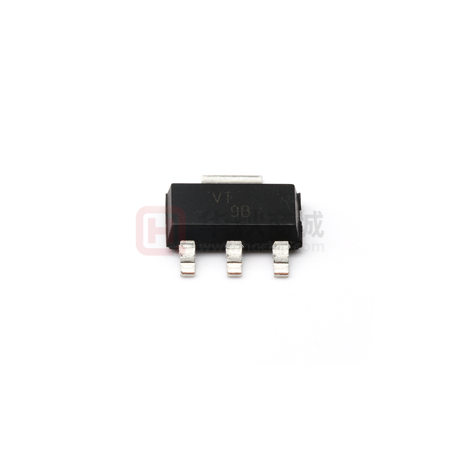
VT
TLV1117-50CDCYG3
ACTIVE
SOT-223
DCY
4
80
RoHS & Green
SN
Level-2-260C-1 YEAR
0 to 125
VT
TLV1117-50CDCYR
ACTIVE
SOT-223
DCY
4
2500
RoHS & Green
SN
Level-2-260C-1 YEAR
0 to 125
VT
TLV1117-50CDCYRG3
ACTIVE
SOT-223
DCY
4
2500
RoHS & Green
SN
Level-2-260C-1 YEAR
0 to 125
VT
TLV1117-50CDRJR
ACTIVE
SON
DRJ
8
3000
RoHS & Green
NIPDAU
Level-2-260C-1 YEAR
0 to 125
ZE50
Addendum-Page 2
ZE25
Samples
�PACKAGE OPTION ADDENDUM
www.ti.com
Orderable Device
13-Aug-2021
Status
(1)
Package Type Package Pins Package
Drawing
Qty
Eco Plan
(2)
Lead finish/
Ball material
MSL Peak Temp
Op Temp (°C)
Device Marking
(3)
(4/5)
(6)
TLV1117-50CKVURG3
ACTIVE
TO-252
KVU
3
2500
RoHS & Green
SN
Level-3-260C-168 HR
0 to 125
TLV1117-50IDCY
ACTIVE
SOT-223
DCY
4
80
RoHS & Green
SN
Level-2-260C-1 YEAR
-40 to 125
VU
TLV1117-50IDCYR
ACTIVE
SOT-223
DCY
4
2500
RoHS & Green
SN
Level-2-260C-1 YEAR
-40 to 125
VU
TLV1117-50IDCYRG3
ACTIVE
SOT-223
DCY
4
2500
RoHS & Green
SN
Level-2-260C-1 YEAR
-40 to 125
VU
TLV1117-50IDRJR
ACTIVE
SON
DRJ
8
1000
RoHS & Green
NIPDAU
Level-2-260C-1 YEAR
-40 to 125
ZF50
TLV1117-50IDRJRG4
ACTIVE
SON
DRJ
8
1000
RoHS & Green
NIPDAU
Level-2-260C-1 YEAR
-40 to 125
ZF50
TLV1117-50IKVURG3
ACTIVE
TO-252
KVU
3
2500
RoHS & Green
SN
Level-3-260C-168 HR
-40 to 125
ZF50
TLV1117CDCY
ACTIVE
SOT-223
DCY
4
80
RoHS & Green
SN
Level-2-260C-1 YEAR
0 to 125
V4
TLV1117CDCYG3
ACTIVE
SOT-223
DCY
4
80
RoHS & Green
SN
Level-2-260C-1 YEAR
0 to 125
V4
TLV1117CDCYR
ACTIVE
SOT-223
DCY
4
2500
RoHS & Green
SN
Level-2-260C-1 YEAR
0 to 125
V4
TLV1117CDCYRG3
ACTIVE
SOT-223
DCY
4
2500
RoHS & Green
SN
Level-2-260C-1 YEAR
0 to 125
V4
TLV1117CDRJR
ACTIVE
SON
DRJ
8
1000
RoHS & Green
NIPDAU
Level-2-260C-1 YEAR
0 to 125
ZYS
TLV1117CKCS
ACTIVE
TO-220
KCS
3
50
RoHS & Green
SN
N / A for Pkg Type
0 to 125
TLV1117C
TLV1117CKCT
ACTIVE
TO-220
KCT
3
50
RoHS &
Non-Green
SN
N / A for Pkg Type
0 to 125
TLV1117C
TLV1117CKTTR
ACTIVE
DDPAK/
TO-263
KTT
3
500
RoHS & Green
SN
Level-3-245C-168 HR
0 to 125
TLV1117C
TLV1117CKTTRG3
ACTIVE
DDPAK/
TO-263
KTT
3
500
RoHS & Green
SN
Level-3-245C-168 HR
0 to 125
TLV1117C
TLV1117CKVURG3
ACTIVE
TO-252
KVU
3
2500
RoHS & Green
SN
Level-3-260C-168 HR
0 to 125
TV1117
TLV1117IDCY
ACTIVE
SOT-223
DCY
4
80
RoHS & Green
SN
Level-2-260C-1 YEAR
-40 to 125
V2
TLV1117IDCYG3
ACTIVE
SOT-223
DCY
4
80
RoHS & Green
SN
Level-2-260C-1 YEAR
-40 to 125
V2
TLV1117IDCYR
ACTIVE
SOT-223
DCY
4
2500
RoHS & Green
SN
Level-2-260C-1 YEAR
-40 to 125
V2
Addendum-Page 3
ZE50
Samples
�PACKAGE OPTION ADDENDUM
www.ti.com
Orderable Device
13-Aug-2021
Status
(1)
Package Type Package Pins Package
Drawing
Qty
Eco Plan
(2)
Lead finish/
Ball material
MSL Peak Temp
Op Temp (°C)
Device Marking
(3)
(4/5)
(6)
TLV1117IDCYRG3
ACTIVE
SOT-223
DCY
4
2500
RoHS & Green
SN
Level-2-260C-1 YEAR
-40 to 125
V2
TLV1117IDRJR
ACTIVE
SON
DRJ
8
1000
RoHS & Green
NIPDAU
Level-2-260C-1 YEAR
-40 to 125
ZYT
TLV1117IKCS
ACTIVE
TO-220
KCS
3
50
RoHS & Green
SN
N / A for Pkg Type
-40 to 125
TLV1117I
TLV1117IKCSE3
ACTIVE
TO-220
KCS
3
50
RoHS & Green
SN
N / A for Pkg Type
-40 to 125
TLV1117I
TLV1117IKTTR
ACTIVE
DDPAK/
TO-263
KTT
3
500
RoHS & Green
SN
Level-3-245C-168 HR
-40 to 125
TLV1117I
TLV1117IKVURG3
ACTIVE
TO-252
KVU
3
2500
RoHS & Green
SN
Level-3-260C-168 HR
-40 to 125
TY1117
(1)
The marketing status values are defined as follows:
ACTIVE: Product device recommended for new designs.
LIFEBUY: TI has announced that the device will be discontinued, and a lifetime-buy period is in effect.
NRND: Not recommended for new designs. Device is in production to support existing customers, but TI does not recommend using this part in a new design.
PREVIEW: Device has been announced but is not in production. Samples may or may not be available.
OBSOLETE: TI has discontinued the production of the device.
(2)
RoHS: TI defines "RoHS" to mean semiconductor products that are compliant with the current EU RoHS requirements for all 10 RoHS substances, including the requirement that RoHS substance
do not exceed 0.1% by weight in homogeneous materials. Where designed to be soldered at high temperatures, "RoHS" products are suitable for use in specified lead-free processes. TI may
reference these types of products as "Pb-Free".
RoHS Exempt: TI defines "RoHS Exempt" to mean products that contain lead but are compliant with EU RoHS pursuant to a specific EU RoHS exemption.
Green: TI defines "Green" to mean the content of Chlorine (Cl) and Bromine (Br) based flame retardants meet JS709B low halogen requirements of