��������
��������
� ������
�
������������
� ���� �� �
���� � ��
� �������
�� �
�
��� ��
���
SGLS171A − JUNE 2003 − REVISED DECEMBER 2003
D Controlled Baseline
D
D
D
D
D
D
D
D
D
D
D TMS320 DSP and Microprocessor SPI and
− One Assembly Site, One Test Site, One
Fabrication Site
Extended Temperature Performance of
−40°C to 125°C
Enhanced Diminishing Manufacturing
Sources (DMS) Support
Enhanced Product-Change Notification
Qualification Pedigree†
Conversion Time ≤ 10 µs
10-Bit-Resolution ADC
Programmable Power-Down
Mode . . . 1 µA
Wide Range Single-Supply Operation of
2.7 V dc to 5.5 V dc
Analog Input Range of 0 V to VCC
Built-in Analog Multiplexer with 8 Analog
Input Channels
† Component qualification in accordance with JEDEC and industry
standards to ensure reliable operation over an extended
temperature range. This includes, but is not limited to, Highly
Accelerated Stress Test (HAST) or biased 85/85, temperature
cycle, autoclave or unbiased HAST, electromigration, bond
intermetallic life, and mold compound life. Such qualification
testing should not be viewed as justifying use of this component
beyond specified performance and environmental limits.
D
D
D
D
D
D
QSPI Compatible Serial Interfaces
End-of-Conversion (EOC) Flag
Inherent Sample-and-Hold Function
Built-In Self-Test Modes
Programmable Power and Conversion Rate
Asynchronous Start of Conversion for
Extended Sampling
Hardware I/O Clock Phase Adjust Input
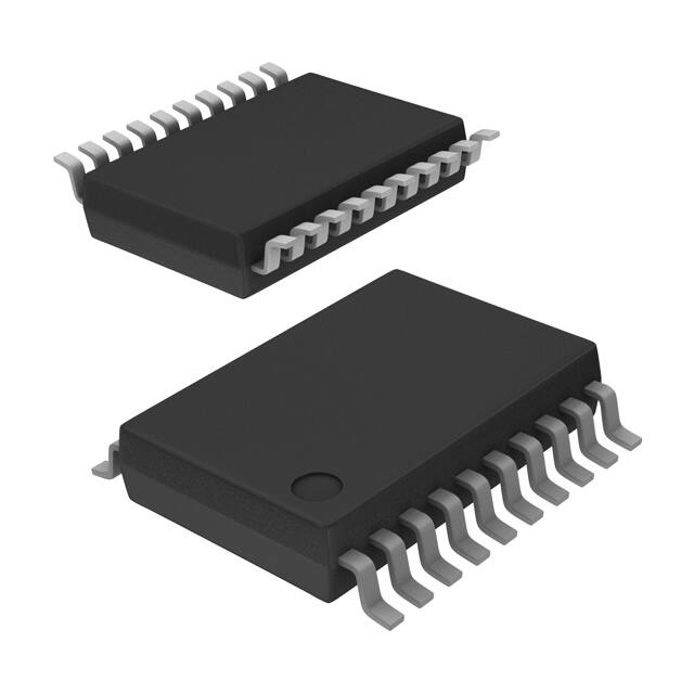
DB PACKAGE
(TOP VIEW)
A0
A1
A2
A3
A4
A5
A6
A7
CSTART
GND
1
2
3
4
5
6
7
8
9
10
20
19
18
17
16
15
14
13
12
11
VCC
EOC
I/O CLK
DATA IN
DATA OUT
CS
REF+
REF−
FS
INV CLK
description
The TLV1548 is a CMOS 10-bit switched-capacitor successive-approximation (SAR) analog-to-digital (A/D)
converter. The device has a chip select (CS), input-output clock (I/O CLK), data input (DATA IN) and serial data
output (DATA OUT) that provides a direct 4-wire synchronous serial peripheral interface (SPI, QSPI) port
of a host microprocessor. When interfacing with a TMS320 DSP, an additional frame sync signal (FS) indicates
the start of a serial data frame. The device allows high-speed data transfers from the host. The INV CLK input
provides further timing flexibility for the serial interface.
In addition to a high-speed converter and versatile control capability, the device has an on-chip 11-channel
multiplexer that can select any one of eight analog inputs or any one of three internal self-test voltages. The
sample-and-hold function is automatic except for the extended sampling cycle, where the sampling cycle is
started by the falling edge of asynchronous CSTART. At the end of the A/D conversion, the end-of-conversion
(EOC) output goes high to indicate that the conversion is complete. The TLV1548 is designed to operate with
a wide range of supply voltages with very low power consumption. The power saving feature is further enhanced
with a software-programmed power-down mode and conversion rate. The converter incorporated in the device
features differential high-impedance reference inputs that facilitate ratiometric conversion, scaling, and
isolation of analog circuitry from logic and supply noise. A switched-capacitor design allows low-error
conversion over the full operating temperature range.
The TLV1548 has eight analog input channels. The TLV1548Q is characterized for operation from −40°C to
125°C.
Please be aware that an important notice concerning availability, standard warranty, and use in critical applications of
Texas Instruments semiconductor products and disclaimers thereto appears at the end of this data sheet.
SPI and QSPI are registered trademarks of Motorola, Inc.
Copyright 2003 Texas Instruments Incorporated
��������� �
�
�������!��� �" #$��%�! �" �� &$'(�#�!��� )�!%*
��)$#!" #������ !� "&%#���#�!���" &%� !+% !%��" �� �%,�" ��"!�$�%�!"
"!��)��) -�����!.*
��)$#!��� &��#%""��/ )�%" ��! �%#%""���(. ��#($)%
!%"!��/ �� �(( &����%!%�"*
POST OFFICE BOX 655303
• DALLAS, TEXAS 75265
1
���������
��������
� ������
�
������������
� ���� �� �
���� � ��
� �������
�� �
�
��� ��
���
SGLS171A − JUNE 2003 − REVISED DECEMBER 2003
functional block diagram
Sample
and
Hold Function
10-Bit ADC
(Switch Capacitors)
CLOCK
A0−A7
REF+
1−8
Output Data Register
14
Analog
MUX
10-to-1
Data Selector
Self-Test
Reference
REF−
DATA IN
16
13
Input
Data
Register
17
19
Control
Logic
and
I/O
Counters
12
15
9
11
18
Terminals shown are for the DB package.
ORDERING INFORMATION
TA
PACKAGE†
ORDERABLE
PART NUMBER
TOP-SIDE
MARKING
−40°C to 125°C
SSOP − DB Tape and reel TLV1548QDBREP
1548QE
† Package drawings, standard packing quantities, thermal data, symbolization, and PCB design
guidelines are available at www.ti.com/sc/package.
2
DATA OUT
POST OFFICE BOX 655303
• DALLAS, TEXAS 75265
EOC
FS
CS
CSTART
INV CLK
I/O CLK
���������
��������
� ������
�
������������
� ���� �� �
���� � ��
� �������
�� �
�
��� ��
���
SGLS171A − JUNE 2003 − REVISED DECEMBER 2003
Terminal Functions
TERMINAL
NAME
NO.
I/O
DESCRIPTION
A0−A3
A4−A7
1−4
5−8
I
Analog inputs. The analog inputs are internally multiplexed. (For a source impedance greater than
1 kΩ, the asynchronous start should be used to increase the sampling time.)
CS
15
I
Chip select. A high-to-low transition on CS resets the internal counters and controls and enables DATA IN, DATA
OUT, and I/O CLK within the maximum setup time. A low-to-high transition disables DATA IN, DATA OUT, and I/O
CLK within the setup time.
CSTART
9
I
Sampling/conversion start control. CSTART controls the start of the sampling of an analog input from a selected
multiplex channel. A high-to-low transition starts the sampling of the analog input signal. A low-to-high transition puts
the sample-and-hold function in hold mode and starts the conversion. CSTART is independent from I/O CLK and
works when CS is high. The low CSTART duration controls the duration of the sampling cycle for the switched
capacitor array. CSTART is tied to VCC if not used.
DATA IN
17
I
Serial data input. The 4-bit serial data selects the desired analog input and test voltage to be converted next in a
normal cycle. These bits can also set the conversion rate and enable the power-down mode.
When operating in the microprocessor mode, the input data is presented MSB first and is shifted in on the first four
rising (INV CLK = VCC) or falling (INV CLK = GND) edges of I/O CLK (after CS↓).
When operating in the DSP mode, the input data is presented MSB first and is shifted in on the first four falling (INV
CLK = VCC) or rising (INV CLK = GND) edges of I/O CLK (after FS↓).
After the four input data bits have been read into the input data register, DATA IN is ignored for the remainder of the
current conversion period.
DATA OUT
16
O
Three-state serial output of the A/D conversion result. DATA OUT is in the high-impedance state when CS is high
and active when CS is low or after FS↓ (in DSP mode). With a valid CS signal, DATA OUT is removed from the
high-impedance state and is driven to the logic level corresponding to the MSB or LSB value of the previous
conversion result. DATA OUT changes on the falling (microprocessor mode) or rising (DSP mode) edge of I/O CLK.
EOC
19
O
End of conversion. EOC goes from a high to a low logic level on the tenth rising (microprocessor mode) or tenth
falling (DSP mode) edge of I/O CLK and remains low until the conversion is complete and data is ready for transfer.
EOC can also indicate that the converter is busy.
FS
12
I
DSP frame synchronization input. FS indicates the start of a serial data frame into or out of the device. FS is tied
to VCC when interfacing the device with a microprocessor.
GND
10
INV CLK
11
Ground return for internal circuitry. All voltage measurements are with respect to GND, unless otherwise noted.
I
Inverted clock input. INV CLK is tied to GND when an inverted I/O CLK is used as the source of the input clock. This
affects both microprocessor and DSP interfaces. INV CLK is tied to VCC if I/O CLK is not inverted. INV CLK can also
invoke a built-in test mode.
POST OFFICE BOX 655303
• DALLAS, TEXAS 75265
3
���������
��������
� ������
�
������������
� ���� �� �
���� � ��
� �������
�� �
�
��� ��
���
SGLS171A − JUNE 2003 − REVISED DECEMBER 2003
Terminal Functions (Continued)
TERMINAL
NAME
NO.
I/O CLK
18
I/O
DESCRIPTION
I
Input/output clock. I/O CLK receives the serial I/O clock input in the two modes and performs the following four
functions in each mode:
Microprocessor mode
•
•
•
•
When INVCLK = VCC, I/O CLK clocks the four input data bits into the input data register on the first four rising
edges of I/O CLK after CS↓ with the multiplexer address available after the fourth rising edge. When INV CLK
= GND, input data bits are clocked in on the first four falling edges instead.
On the fourth falling edge of I/O CLK, the analog input voltage on the selected multiplex input begins charging
the capacitor array and continues to do so until the tenth rising edge of I/O CLK except in the extended sampling
cycle where the duration of CSTART determines when to end the sampling cycle.
Output data bits change on the first ten falling I/O clock edges regardless of the condition of INV CLK.
I/O CLK transfers control of the conversion to the internal state machine on the tenth rising edge of I/O CLK
regardless of the condition of INV CLK.
Digital signal processor (DSP) mode
•
•
•
•
When INV CLK = VCC, I/O CLK clocks the four input data bits into the input data register on the first four falling
edges of I/O CLK after FS↓ with the multiplexer address available after the fourth falling edges. When INV CLK
= GND, input data bits are clocked in on the first four rising edges instead.
On the fourth rising edge of I/O CLK, the analog input voltage on the selected multiplex input begins charging
the capacitor array and continues to do so until the tenth falling edge of I/O CLK except in the extended sampling
cycle where the duration of CSTART determines when to end the sampling cycle.
Output data MSB shows after FS↓ and the rest of the output data bits change on the first ten rising I/O CLK edges
regarless of the condition of INV CLK.
I/O CLK transfers control of the conversion to the internal state machine on the tenth falling edge of I/O CLK
regardless of the condition of INV CLK.
REF+
14
I
Upper reference voltage (nominally VCC ). The maximum input voltage range is determined by the difference between
the voltages applied to REF+ and REF−.
REF−
13
I
Lower reference voltage (nominally ground)
VCC
20
I
Positive supply voltage
detailed description
Initially, with CS high (inactive), DATA IN and I/O CLK are disabled and DATA OUT is in the high-impedance
state. When the serial interface takes CS low (active), the conversion sequence begins with the enabling of I/O
CLK and DATA IN and the removal of DATA OUT from the high-impedance state. The host then provides the
4-bit channel address to DATA IN and the I/O clock sequence to I/O CLK. During this transfer, the host serial
interface also receives the previous conversion result from DATA OUT. I/O CLK receives an input sequence from
the host that is from 10 to 16 clocks long. The first four valid I/O CLK cycles load the input data register with the
4-bit input data on DATA IN that selects the desired analog channel. The next six clock cycles provide the control
timing for sampling the analog input. Sampling of the analog input is held after the first valid I/O CLK sequence
of ten clocks. The tenth clock edge also takes EOC low and begins the conversion. The exact locations of the
I/O clock edges depend on the mode of operation.
serial interface
The TLV1548 is compatible with generic microprocessor serial interfaces such as SPI and QSPI, and a TMS320
DSP serial interface. The internal latched flag If_mode is generated by sampling the state of FS at the falling
edge of CS. If_mode is set to one (for microprocessor) when FS is high at the falling edge of CS, and If_mode
is cleared to zero (for DSP) when FS is low at the falling edge of CS. This flag controls the multiplexing of I/O
CLK and the state machine reset function. FS is pulled high when interfacing with a microprocessor.
4
POST OFFICE BOX 655303
• DALLAS, TEXAS 75265
���������
��������
� ������
�
������������
� ���� �� �
���� � ��
� �������
�� �
�
��� ��
���
SGLS171A − JUNE 2003 − REVISED DECEMBER 2003
I/O CLK
The I/O CLK can go up to 10 MHz for most of the voltage range when fast I/O is possible. The maximum I/O
CLK is limited to 2.8 MHz for a supply voltage range from 2.7 V. Table 1 lists the maximum I/O CLK frequencies
for all different supply voltage ranges. This also depends on input source impedance. For example, I/O CLK
speed faster than 2.39 MHz is achievable if the input source impedance is less than 1 kΩ.
Table 1. Maximum I/O CLK Frequency
VCC
MAXIMUM INPUT
RESISTANCE (Max)
2.7 V
5K
4.5 V
1K
SOURCE IMPEDANCE
I/O CLK
1 kΩ
2.39 MHz
100 Ω
2.81 MHz
1 kΩ
7.18 MHz
100 Ω
10 MHz
microprocessor serial interface
Input data bits from DATA IN are clocked in on the first four rising edges of the I/O CLK sequence if INV CLK
is held high when the device is in microprocessor interface mode. Input data bits are clocked in on the first four
falling edges of the I/O CLK sequence if INV CLK is held low. The MSB of the previous conversion appears on
DATA OUT on the falling edge of CS. The remaining nine bits are shifted out on the next nine edges (depending
on the state of INV CLK) of I/O CLK. Ten bits of data are transmitted to the host through DATA OUT.
A minimum of 9.5 clock pulses is required for the conversion to begin. On the tenth clock rising edge, the EOC
output goes low and returns to the high logic level when the conversion is complete; then the result can be read
by the host. On the tenth clock falling edge, the internal logic takes DATA OUT low to ensure that the remaining
bit values are zero if the I/O CLK transfer is more than ten clocks long.
CS is inactive (high) between serial I/O CLK transfers. Each transfer takes at least ten I/O CLK cycles. The falling
edge of CS begins the sequence by removing DATA OUT from the high-impedance state. The rising edge of
CS ends the sequence by returning DATA OUT to the high-impedance state within the specified delay time. Also,
the rising edge of CS disables I/O CLK and DATA IN within a setup time. A conversion does not begin until the
tenth I/O CLK rising edge.
A high-to-low transition on CS within the specified time during an ongoing cycle aborts the cycle, and the device
returns to the initial state (the output data register holds the previous conversion result). CS should not be taken
low close to completion of conversion because the output data can be corrupted.
POST OFFICE BOX 655303
• DALLAS, TEXAS 75265
5
���������
��������
� ������
�
������������
� ���� �� �
���� � ��
� �������
�� �
�
��� ��
���
SGLS171A − JUNE 2003 − REVISED DECEMBER 2003
DSP interface
The TLV1548 can also interface with a DSP, from the TMS320 family for example, through a serial port. The
analog-to-digital converter (ADC) serves as a slave device where the DSP supplies FS and the serial I/O CLK.
Transmit and receive operations are concurrent. The falling edge of FS must occur no later than seven I/O CLK
periods after the falling edge of CS.
DSP I/O cycles differ from microprocessor I/O cycles in the following ways:
D When interfaced with a DSP, the output data MSB is available after FS↓. The remaining output data changes
on the rising edge of I/O CLK. The input data is sampled on the first four falling edges of I/O CLK after FS↓
and when INV CLK is high, or the first four rising edges of I/O CLK after FS↓ and when INV CLK is low. This
operation is inverted when interfaced with a microprocessor.
D A new DSP I/O cycle is started on the rising edge of I/O CLK after the rising edge of FS. The internal state
machine is reset on each falling edge of I/O CLK when FS is high. This operation is opposite when interfaced
with a microprocessor.
D The TLV1548 supports a 16-clock cycle when interfaced with a DSP. The output data is padded with six
trailing zeros when it is operated in DSP mode.
Table 2. TLV1548 Serial Interface Modes
INTERFACE MODE
I/O
DSP ACTION
CS↓
Initializes counter
Samples state of FS
CS↑
Resets state machine and disable I/O
Disables I/O
Connects to VCC
Connects to DSP FSX output
Initializes the state machine at each CLK↓ after FS↑
Starts a new cycle at each CLK↑ following the initialization
(initializes the counter)
I/O CLK
Starts sampling of the analog input started at fourth I/O CLK↑
Conversion started at tenth I/O CLK↑
Starts sampling of the analog input at fourth I/O CLK↓
Starts sampling of the analog input at tenth I/O CLK↓
DATA IN
Samples input data on I/O CLK↑ (INV CLK high)
Samples input data on I/O CLK↓ (INV CLK low)
Samples input data at I/O CLK↓ (INV CLK high)
Samples input data at I/O CLK↑ (INV CLK low)
Makes MSB available on CS↓
Changes remaining data on I/O CLK↓
Makes MSB available FS↓
Changes remaining data at each following I/O CLK↑ after
FS↓
FS
DATA OUT
6
MICROPROCESSOR ACTION
POST OFFICE BOX 655303
• DALLAS, TEXAS 75265
���������
��������
� ������
�
������������
� ���� �� �
���� � ��
� �������
�� �
�
��� ��
���
SGLS171A − JUNE 2003 − REVISED DECEMBER 2003
input data bits
DATA IN is internally connected to a 4-bit serial input data register. The input data selects a different mode or
selects different analog input channels. The host provides the data word with the MSB first. Each data bit clocks
in on the edge (rising or falling depending on the status of INV CLK and FS) of the I/O CLK sequence. The input
clock can be inverted by grounding INV CLK (see Table 3 for the list of software programmed operations set
by the input data).
Table 3. TLV1548 Software-Programmed Operation Modes
INPUT DATA BYTE
A3 − A0
FUNCTION SELECT
COMMENT
BINARY
HEX
Analog channel A0 for TLV1548 selected
0000b
0h
Analog channel A1 for TLV1548 selected
0001b
1h
Analog channel A2 for TLV1548 selected
0010b
2h
Analog channel A3 for TLV1548 selected
0011b
3h
Analog channel A4 for TLV1548 selected
0100b
4h
Analog channel A5 for TLV1548 selected
0101b
5h
Analog channel A6 for TLV1548 selected
0110b
6h
Analog channel A7 for TLV1548 selected
0111b
7h
Software power down set
1000b
8h
No conversion result (cleared by any access)
Fast conversion rate (10 µs) set
1001b
9h
No conversion result (cleared by setting to fast)
Slow conversion rate (40 µs) set
1010b
Ah
No conversion result (cleared by setting to slow)
Self-test voltage (Vref) − Vref−)/2 selected
1011b
Bh
Output result = 200h
Self-test voltage Vref* selected
1100b
Ch
Output result = 000h
Self-test voltage Vref) selected
1101b
Dh
Output result = 3FFh
Reserved
1110b
Eh
No conversion result
Reserved
1111b
Fh
No conversion result
analog inputs and internal test voltages
The eight analog inputs and the three internal test inputs are selected by the 11-channel multiplexer according
to the input data bit as shown in Table 3. The input multiplexer is a break-before-make type to reduce
input-to-input noise injection resulting from channel switching.
The device can be operated in two distinct sampling modes: normal sampling mode (fixed sampling time) and
extended sampling mode (flexible sampling time). When CSTART is held high, the device is operated in normal
sampling mode. When operated in normal sampling mode, sampling of the analog input starts on the rising edge
of the fourth I/O CLK pulse in the microprocessor interface mode (and on the fourth falling edge of I/O CLK in
the DSP interface mode). Sampling continues for 6 I/O CLK periods. The sample is held on the falling edge of
the tenth I/O CLK pulse in the microprocessor interface mode. The sample is held on the falling edge of the tenth
I/O CLK pulse in the DSP interface mode.The three test inputs are applied to the multiplexer, then sampled and
converted in the same manner as the external analog inputs.
POST OFFICE BOX 655303
• DALLAS, TEXAS 75265
7
���������
��������
� ������
�
������������
� ���� �� �
���� � ��
� �������
�� �
�
��� ��
���
SGLS171A − JUNE 2003 − REVISED DECEMBER 2003
converter
The CMOS threshold detector in the successive-approximation conversion system determines the value of
each bit by examining the charge on a series of binary-weighted capacitors (see Figure 1). In the first phase
of the conversion process, the analog input is sampled by closing the SC switch and all ST switches
simultaneously. This action charges all of the capacitors to the input voltage.
In the next phase of the conversion process, all ST and SC switches are opened and the threshold detector
begins identifying bits by identifying the charge (voltage) on each capacitor relative to the reference (REF −)
voltage. In the switching sequence, ten capacitors are examined separately until all ten bits are identified and
then the charge-convert sequence is repeated. In the first step of the conversion phase, the threshold detector
looks at the first capacitor (weight = 512). Node 512 of this capacitor is switched to the REF+ voltage, and the
equivalent nodes of all the other capacitors on the ladder are switched to REF −. If the voltage at the summing
node is greater than the trip point of the threshold detector (approximately one-half VCC), a bit 0 is placed in the
output register and the 512-weight capacitor is switched to REF −. If the voltage at the summing node is less
than the trip point of the threshold detector, a bit 1 is placed in the register and the 512-weight capacitor remains
connected to REF + through the remainder of the successive-approximation process. The process is repeated
for the 256-weight capacitor, the 128-weight capacitor, and so forth down the line until all bits are counted.
With each step of the successive-approximation process, the initial charge is redistributed among the
capacitors. The conversion process relies on charge redistribution to count and weigh the bits from MSB to LSB.
SC
Threshold
Detector
To Output
Latches
512
Node 512
REF −
256
128
8
REF+
REF+
REF+
REF −
ST
REF −
ST
REF −
ST
4
2
REF+
REF+
REF −
ST
1
REF −
ST
1
REF+
REF −
ST
REF+
REF −
ST
ST
VI
Figure 1. Simplified Model of the Successive-Approximation System
8
POST OFFICE BOX 655303
• DALLAS, TEXAS 75265
���������
��������
� ������
�
������������
� ���� �� �
���� � ��
� �������
�� �
�
��� ��
���
SGLS171A − JUNE 2003 − REVISED DECEMBER 2003
extended sampling, asynchronous start of sampling: CSTART operation
The extended sampling mode of operation programs the acquisition time (tACQ) of the sample-and-hold circuit.
This allows the analog inputs of the device to be directly interfaced to a wide range of input source impedances.
The extended sampling mode consumes higher power depending on the duration of the sampling period
chosen.
CSTART controls the sampling period and starts the conversion. The falling edge of CSTART initiates the
sampling period of a preset channel. The low time of CSTART controls the acquisition time of the input
sample-and-hold circuit. The sample is held on the rising edge of CSTART. Asserting CSTART causes the
converter to perform a new sample of the signal on the preset valid MUX channel (one of the eight) and discard
the current conversion result ready for output. Sampling continues as long as CSTART is active (negative). The
rising edge of CSTART ends the sampling cycle. The conversion cycle starts two internal system clocks after
the rising edge of CSTART.
Once the conversion is complete, the processor can initiate a normal I/O cycle to read the conversion result and
set the MUX address for the next conversion. Since the internal flag AsyncFlag is set high, this flag setting
indicates the cycle is an output cycle, so no conversion is performed during the cycle. The internal state machine
tests the AsyncFlag on the falling edge of CS. AsyncFlag is set high at the rising edge of CSTART, and it is reset
low at the rising edge of each CS. A conversion cycle follows a sampling cycle only if AsyncFlag is tested as
low at the falling edge of CS. As shown in Figure 2, an asynchronous I/O cycle can be removed by two
consecutive normal I/O cycles.
Table 4. TLV1548 Hardware Configuration for Different Operating Modes
CS
CSTART
AsyncFlag at CS↓
Normal sampling
OPERATING MODES
Low
High
Low
Fixed 6 I/O CLK sampling, synchronous conversion follows
Normal I/O (read out only)
Low
High
High
No sampling, no conversion
Extended sampling
High
Low
N/A
Flexible sampling period controlled by CSTART,
asynchronous conversion follows
POST OFFICE BOX 655303
ACTION
• DALLAS, TEXAS 75265
9
���������
��������
� ������
�
������������
� ���� �� �
���� � ��
� �������
�� �
�
��� ��
���
SGLS171A − JUNE 2003 − REVISED DECEMBER 2003
Complete Extended
Sample Cycle
Extended
Sample
Cycle
Normal
Cycle
Extended
Sample
Cycle
Read Out
Cycle
Read Out
Cycle
Read Out
Cycle
Normal
Cycle
CS
FS
(DSP Mode)
tACQ
tACQ
ÎÎÎÎÎÎÎÎÎÎÎÎÎÎÎÎÎÎÎÎÎÎÎÎÎÎÎÎÎÎÎ
ÎÎÎÎÎÎÎÎÎÎÎÎÎÎÎÎÎÎÎÎÎÎÎÎÎÎÎÎÎÎÎ
ÎÎÎÎÎÎÎÎÎÎÎÎÎÎÎÎÎÎÎÎÎÎÎÎÎÎÎÎÎÎÎ
CSTART
DATA IN
Aa
Ab
Ab
Ac
Ad
EOC
DATA OUT
Hi−Z
Hi−Z
Hi−Z
X
Da
Hi−Z
Db
Hi−Z
Db
Hi−Z
Dc
Async Flag
NOTES: A. Aa = Address for input channel a.
B. Da = Conversion result from channel a.
Figure 2. Extended Sampling Operation
reference voltage inputs
There are two reference inputs used with the TLV1548, REF+ and REF−. These voltage values establish the
upper and lower limits of the analog inputs to produce a full-scale and zero-scale reading respectively. The
values of REF+, REF−, and the analog input should not exceed the positive supply or be lower than GND
consistent with the specified absolute maximum ratings. The digital output is at full scale when the input signal
is equal to or higher than REF+ and is at zero when the input signal is equal to or lower than REF−.
programmable conversion rate
The TLV1548 offers two conversion rates to maximize battery life when high-speed operation is not necessary.
The conversion rate is programmable. Once the conversion rate has been selected, it takes effect immediately
in the same cycle and stays at the same rate until the other rate is chosen. The conversion rate should be set
at power up. Activation and deactivation of the power-down state (digital logic active) has no effect on the preset
conversion rate.
10
POST OFFICE BOX 655303
• DALLAS, TEXAS 75265
���������
��������
� ������
�
������������
� ���� �� �
���� � ��
� �������
�� �
�
��� ��
���
SGLS171A − JUNE 2003 − REVISED DECEMBER 2003
Table 5. Conversion Rate and Power Consumption Selection
TYPICAL SUPPLY CURRENT, ICC
CONVERSION TIME,
tconv
AVAILABLE VCC
RANGE
Fast conversion speed
7 µs typ
5.5 V to 3.3 V
9h
0.6 mA typ
1.5 mA max
1 µA typ
Slow conversion speed
15 µs typ
5.5 V to 2.7 V
Ah
0.4 mA typ
1 mA max
1 µA typ
CONVERSION RATE
INPUT DATA
OPERATING
POWER
DOWN
programmable power-down state
The device is put into the power-down state by writing 8h to DATA IN. The power-up state is restored during
the next active access by pulling CS low. The conversion rate selected before the device is put into the
power-down state is not affected by the power-down mode. Power-down can be used to achieve even lower
power consumption. This is because the sustaining power (when not converting) is only 1.3 mA maximum and
standby power is only 1 µA maximum. (By averaging out the power consumption can be much lower than the
1 mA peak when the conversion throughput is lower.)
Power Down
CS
ÎÎÎÎÎÎÎÎÎÎÎÎÎÎÎÎ
ÎÎÎÎÎÎÎÎÎÎÎÎÎÎÎÎ
Hi-Z
DATA IN
ÎÎÎÎÎÎÎÎÎ
ÎÎÎÎÎÎÎÎÎ
Hi-Z
1 0 0 0
EOC
Supply Current
ICC
0
ÎÎÎÎÎÎÎÎÎÎÎÎÎÎÎÎÎÎÎÎÎÎÎÎ
ÎÎÎÎÎÎÎÎÎÎÎÎÎÎÎÎÎÎÎÎÎÎÎÎ
ÎÎÎÎÎÎÎÎÎÎÎÎÎÎÎÎÎÎÎÎÎÎÎÎ
ÎÎÎÎÎÎÎÎÎÎÎÎÎÎÎÎÎÎÎÎÎÎÎÎ
ÎÎÎÎÎÎÎÎÎÎÎÎÎÎÎÎÎÎÎÎÎÎÎÎ
1 mA
(Typical Peak Supply)
0.3 mA
(Typical Sustaining)
0.0007 mA
(Typical Power Down
Supply)
Figure 3. Typical Supply Current During Conversion/Power Down
power up and initialization
After power up, if operating in DSP mode, CS and FS must be taken from high to low to begin an I/O cycle. EOC
is initially high, and the input data register is set to all zeroes. The content of the output data register is random,
and the first conversion result should be ignored. For initialization during operation, CS is taken high and
returned low to begin the next I/O cycle. The first conversion after the device has returned from the power-down
state can be invalid and should be disregarded.
When power is first applied to the device, the conversion rate must be programmed, and the internal Async Flag
must be taken low once. The rising edge of CS of the same cycle then takes Async Flag low.
POST OFFICE BOX 655303
• DALLAS, TEXAS 75265
11
���������
��������
� ������
�
������������
� ���� �� �
���� � ��
� �������
�� �
�
��� ��
���
SGLS171A − JUNE 2003 − REVISED DECEMBER 2003
First Cycle After Powerup
MUX Address for Channel 0
CS
FS
(For DSP Mode)
Async Flag
(Internal)
DATA IN
ÎÎÎÎ
ÎÎÎÎ
ÎÎÎÎ
ÎÎÎÎÎÎÎÎÎÎÎÎÎÎÎÎ
ÎÎÎÎÎÎÎÎÎÎÎÎÎÎÎÎ
ÎÎÎÎÎÎÎÎÎÎÎÎÎÎÎÎ
9h
0h
Ab
Signal Channel 0 Converted
EOC
DATA OUT
Hi−Z
Hi−Z
X
Conversion Rate Set to Fast
Hi−Z
Hi−Z
D0
X
Conversion Result From Channel 0
AsyncFlag Reset Low
Figure 4. Power Up Initialization
input clock inversion − INV CLK
The input data register uses I/O CLK as the source of the sampling clock. This clock can be inverted to provide
more setup time. INV CLK can invert the clock. When INV CLK is grounded, the input clock for the input data
register is inverted. This allows an additional one-half I/O CLK period for the input data setup time. This is useful
for some serial interfaces. When the input sampling clock is inverted, the output data changes at the same time
that the input data is sampled.
Table 6. Function of INV CLK
CONDITION
CLOCK
OUTPUT DATA
CHANGES ON
INPUT DATA
SAMPLED ON
High (MP† mode)
Low (DSP‡ mode)
↓
↑
↑
↓
High (MP† mode)
Low (DSP‡ mode)
↓
↓
↑
↑
INV CLK
FS at CS↓
High
High
Low
I/O CLK ACTIVE EDGE
Low
† MP = microprocessor mode
‡ DSP = digital signal processor mode
12
POST OFFICE BOX 655303
• DALLAS, TEXAS 75265
���������
��������
� ������
�
������������
� ���� �� �
���� � ��
� �������
�� �
�
��� ��
���
SGLS171A − JUNE 2003 − REVISED DECEMBER 2003
Threshold
Detect
REF+
REF−
SampleandHold
Function
A0−A7
11-to-1
Analog
MUX
TEST 0−2
DATA OUT
Output Shift Clock
Invert
Vref
REF−
SAR† Latch
10-to-1 Select
Conversion
Clock
REF+
EOC
INV CLK
If_mode
DATA IN
If_mode
OSC
Input
Data
Register
SMCLK
Input Shift Clock
2-to-1
Invert
2-to-1
DSP§
If_mode
CS
FS
I/O CLK
Control
State
Machine
Microprocessor‡
† Successive approximation register
‡ If_mode = 1, microprocessor interface mode
§ If_mode = 0, DSP interface mode
Figure 5. Clock Scheme
absolute maximum ratings over operating free-air temperature range (unless otherwise noted)†
Supply voltage range, VCC (see Note 1) . . . . . . . . . . . . . . . . . . . . . . . . . . . . . . . . . . . . . . . . . . . . . −0.5 V to 6.5 V
Input voltage range, VI (any input) . . . . . . . . . . . . . . . . . . . . . . . . . . . . . . . . . . . . . . . . . . . . . −0.3 V to VCC + 0.3 V
Output voltage range, VO . . . . . . . . . . . . . . . . . . . . . . . . . . . . . . . . . . . . . . . . . . . . . . . . . . . . −0.3 V to VCC + 0.3 V
Positive reference voltage, Vref + . . . . . . . . . . . . . . . . . . . . . . . . . . . . . . . . . . . . . . . . . . . . . . . . . . . . . . VCC + 0.1 V
Negative reference voltage, Vref − . . . . . . . . . . . . . . . . . . . . . . . . . . . . . . . . . . . . . . . . . . . . . . . . . . . . . . . . . . −0.1 V
Peak input current, II (any input) . . . . . . . . . . . . . . . . . . . . . . . . . . . . . . . . . . . . . . . . . . . . . . . . . . . . . . . . . . ±20 mA
Peak total input current (all inputs) . . . . . . . . . . . . . . . . . . . . . . . . . . . . . . . . . . . . . . . . . . . . . . . . . . . . . . . . −30 mA
Operating free-air temperature range, TA: TLV1548Q . . . . . . . . . . . . . . . . . . . . . . . . . . . . . . . . −40°C to 125°C
Storage temperature range, Tstg . . . . . . . . . . . . . . . . . . . . . . . . . . . . . . . . . . . . . . . . . . . . . . . . . . . −65°C to 150°C
Thermal resistance, Junction-to-Air, θJA . . . . . . . . . . . . . . . . . . . . . . . . . . . . . . . . . . . . . . . . . . . . . . . . 114.2°C/W
Lead temperature 1,6 mm (1/16 inch) from the case for 10 seconds . . . . . . . . . . . . . . . . . . . . . . . . . . . . 260°C
† Stresses beyond those listed under “absolute maximum ratings” may cause permanent damage to the device. These are stress ratings only, and
functional operation of the device at these or any other conditions beyond those indicated under “recommended operating conditions” is not
implied. Exposure to absolute-maximum-rated conditions for extended periods may affect device reliability.
NOTE 1: All voltage values are with respect to GND with REF − and GND wired together (unless otherwise noted).
POST OFFICE BOX 655303
• DALLAS, TEXAS 75265
13
���������
��������
� ������
�
������������
� ���� �� �
���� � ��
� �������
�� �
�
��� ��
���
SGLS171A − JUNE 2003 − REVISED DECEMBER 2003
recommended operating conditions
MIN
Supply voltage, VCC
NOM
2.7
Positive reference voltage, Vref + (see Note 2)
MAX
5.5
VCC
0
Negative reference voltage, Vref − (see Note 2)
Differential reference voltage, Vref + − Vref − (see Note 2)
2.5
Analog input voltage, VI (analog) (see Note 2)
VCC
0
High-level control input voltage, VIH
V
V
V
VCC +0.2
VCC
2.1
V
V
V
Low-level control input voltage, VIL
0.6
Setup time, input data bits valid before I/O CLK↑↓, tsu(A) (see Figure 9)
UNIT
100
V
ns
Hold time, input data bits valid after I/O CLK↑↓, th(A) (see Figure 9)
5
30
ns
Setup time, CS↓ to I/O CLK↑, tsu(CS)
See Figure 10 and Note 3
5
30
ns
Hold time, I/O CLK↓ to CS↑, th(CS)
See Figure 10
65
ns
Pulse duration, FS high, twH(FS)
See Figure 14
1
I/O CLK
periods
Pulse duration, CSTART, tw(CSTART)
Source impedance ≤ 1 kΩ,
See Figure 15
Setup time, CS↑ to CSTART↓, tsu(CSTART)
See Figure 15
10
0.1
6
10
Clock frequency at I/O CLK, fCLK
VCC = 5.5 V
VCC = 2.7 V
0.1
2
2.81
Pulse duration, I/O CLK high, twH(I/O)
VCC = 5.5 V
VCC = 2.7 V
100
Pulse duration, I/O CLK low, twL(I/O)
VCC = 5.5 V
VCC = 2.7 V
100
Operating free-air temperature, TA
TLV1548Q
−40
VCC = 5.5 V,
µs
0.84
ns
MHz
50
ns
50
ns
125
°C
Junction temperature, TJ
TLV1548Q
150
°C
NOTES: 2. Analog input voltages greater than the voltage applied to REF+ convert as all ones (1111111111), while input voltages less than the
voltage applied to REF− convert as all zeros (0000000000). The device is functional with reference (Vref+ − Vref−) down to 1 V;
however, the electrical specifications are no longer applicable.
3. To minimize errors caused by noise at CS↓, the internal circuitry waits for a setup time after CS↓ before responding to control input
signals. No attempt should be made to clock in an input dat until the minimum CS setup time has elapsed.
14
POST OFFICE BOX 655303
• DALLAS, TEXAS 75265
���������
��������
� ������
�
������������
� ���� �� �
���� � ��
� �������
�� �
�
��� ��
���
SGLS171A − JUNE 2003 − REVISED DECEMBER 2003
electrical characteristics over recommended operating free-air temperature range,
VCC = Vref+ = 2.7 V to 5.5 V, I/O CLK frequency = 2.2 MHz (unless otherwise noted)
PARAMETER
TEST CONDITIONS
TYP†
MAX
UNIT
VOH
High-level output voltage
VCC = 5.5 V,
VCC = 2.7 V,
VOL
Low-level output voltage
VCC = 5.5 V,
VCC = 2.7 V,
IOL = 0.8 mA
IOL = 20 µA
CS = VCC
2.5
High-impedance output current
VO = VCC,
VO = 0,
1
IOZ
CS = VCC
−1
−2.5
IIH
IIL
High-level input current
0.005
2.5
µA
−0.005
2.5
µA
VCC = 3.3 V to 5.5 V
0.6
1.5
VCC = 3.3 V to 5.5 V
0.4
1
VCC = 2.7 V to 3.3 V
0.35
0.75
ICC
ICC(ES)
Low-level input current
Operating supply current
Extended sampling mode
operating current
ICC(ST)
Sustaining supply current
ICC(PD)
Power-down supply current
Ilkg
Selected channel leakage current
Maximum static analog
reference current into REF+
IOH = −0.2 mA
IOH = −20 µA
MIN
VI = VCC
VI = 0
Conversion speed = fast,
For all digital inputs,
0 ≤ VI ≤ 0.3 V or
VI ≥ VCC − 0.3 V
Conversion speed = slow,
For all digital inputs,
0 ≤ VI ≤ 0.3 V or
VI ≥ VCC − 0.3 V
2.4
V
2.4
0.4
0.1
V
µA
A
mA
VCC = 3.3 V to 5.5 V
VCC = 2.7 V to 3.3 V
Conversion speed = slow,
For all digital inputs,
VCC = 2.7 V to 3.3 V
0 ≤ VI ≤ 0.3 V or
VI ≥ VCC − 0.3 V
For all digital inputs,
0 ≤ VI ≤ 0.3 V or VI ≥ VCC − 0.3 V
1.5
mA
1
mA
0.3
mA
25
µA
Selected channel at VCC, unselected channel at 0 V
1
µA
Selected channel at 0 V, unselected channel at VCC
−1
µA
1
µA
Vref + = VCC = 5.5 V,
1
Vref − = GND
Input capacitance, analog inputs
20
55
Ci
Input capacitance, control inputs
20
15
Zi
Input multiplexer on resistance
VCC = 4.5 V
VCC = 2.7 V
1
5
pF
kΩ
† All typical values are at VCC = 5 V, TA = 25°C.
POST OFFICE BOX 655303
• DALLAS, TEXAS 75265
15
���������
��������
� ������
�
������������
� ���� �� �
���� � ��
� �������
�� �
�
��� ��
���
SGLS171A − JUNE 2003 − REVISED DECEMBER 2003
operating characteristics over recommended operating free-air temperature range,
VCC = Vref+ = 2.7 V to 5.5 V, I/O CLK frequency = 2.2 MHz (unless otherwise noted)
TEST
CONDITIONS
PARAMETER
MIN
TYP†
MAX
UNIT
±0.5
±1
LSB
±0.5
±1
LSB
EL
ED
Linearity error (see Note 6)
Differential linearity error
See Note 2
EO
EG
Offset error (see Note 7)
See Note 2
±1.5
LSB
Gain error (see Note 7)
See Note 2
±1
LSB
ET
Total unadjusted error (see Note 8)
±1.75
LSB
Self-test output code (see Table 3 and Note 9)
Fast conversion speed
tconv
tc
Conversion time
Slow conversion speed
Total cycle time (access,
sample, conversion and EOC↑
to CS↓ delay)
DATA IN = 1011
512
DATA IN - 1100
0
DATA IN = 1101
1023
See Figures 16
through 19
7
10
µs
15
25
µs
Fast conversion speed
See Figures 15
through 19 and
Notes 10, 11, 12
10.1 +
10 I/O CLK
Slow conversion speed
See Figures 15
through 19 and
Notes 10 and 12
40.1 +
10 I/O CLK
µss
tacq
Channel acquisition time (sample)
See Figures 15
through 18 and
Note 10
tv
td1(FS)
Valid time, DATA OUT remains valid after I/O CLK↓
See Figure 11
Delay time, I/O CLK high to FS high
See Figure 14
5
30
50
ns
td2(FS)
Delay time, I/O CLK high to FS low
See Figure 14
10
30
60
ns
td(EOC↑ − CS↓)
Delay time, EOC↑ to CS low
See Figure 15
and Note 5
100
td(CS↓ − FS↑)
Delay time, CS↓ to FS↑
See Figures 12
and 18
td(I/O -CS)
Delay time, 10th I/O CLK low to CS low to abort
conversion (see Note 13)
See Figure 10
6
20
1
I/O CLK
periods
ns
ns
7
1.1
I/O CLK
periods
µs
† All typical values are at TA = 25°C.
NOTES: 2. Analog input voltages greater than that applied to REF + convert as all ones (1111111111), while input voltages less than that applied
to REF − convert as all zeros (0000000000). The device is functional with reference down to 1 V (Vref+ − Vref − 1); however, the
electrical specifications are no longer applicable.
5. For all operating modes.
6. Linearity error is the maximum deviation from the best straight line through the A/D transfer characteristics.
7. Zero error is the difference between 0000000000 and the converted output for zero input voltage. Full-scale error is the difference
between 1111111111 and the converted output for full-scale input voltage.
8. Total unadjusted error comprises linearity, zero-scale, and full-scale errors.
9. Both the input data and the output codes are expressed in positive logic.
10. I/O CLK period = 1 /(I/O CLK frequency) (see Figure 8).
11. For 3.3 V to 5.5 V only
12. For microprocessor mode
13. Any transitions of CS are recognized as valid only when the level is maintained for a setup time after the transition.
16
POST OFFICE BOX 655303
• DALLAS, TEXAS 75265
���������
��������
� ������
�
������������
� ���� �� �
���� � ��
� �������
�� �
�
��� ��
���
SGLS171A − JUNE 2003 − REVISED DECEMBER 2003
operating characteristics over recommended operating free-air temperature range,
VCC = Vref+ = 2.7 V to 5.5 V, I/O CLK frequency = 2.2 MHz (unless otherwise noted) (continued)
PARAMETER
TEST CONDITIONS
MIN
TYP†
MAX
Delay time, I/O CLK low to DATA OUT valid
See Figure 11
Delay time, 10th I/O CLK↓ to EOC low
See Figure 13
70
240
ns
tPZH, tPZL
tPHZ, tPLZ
Enable time, CS low to DATA OUT valid (MSB driven)
See Figure 8
0.7
1.3
µs
Disable time, CS high to DATA OUT invalid (high impedance)
See Figure 8
70
150
ns
tf(EOC)
tr(bus)
Fall time, EOC
See Figure 13
15
50
ns
Rise time, output data bus at 2.2 MHz I/O CLK
See Figure 11
50
250
ns
See Figure 11
50
250
ns
tf(bus)
Fall time, output data bus at 2.2 MHz I/O CLK
† All typical values are at TA = 25°C.
60
UNIT
td(I/O-DATA)
td(I/O-EOC)
ns
PARAMETER MEASUREMENT INFORMATION
15 V
C1
10 µF
C2
0.1 µF
EOC
TLV1548
_
U1
+
VI
Ax
D0
−15 V
C1
10 µF
LOCATION
U1
C1
C2
C2
0.1 µF
DESCRIPTION
OP27
10-µF 35-V tantalum capacitor
0.1-µF ceramic NPO SMD capacitor
PART NUMBER
—
—
AVX 12105C104KA105 or equivalent
Figure 6. Analog Input Buffer to Analog Inputs
VCC
Test Point
VCC
Test Point
RL = 2.18 kΩ
RL = 2.18 kΩ
EOC
CL = 50 pF
DATA OUT
12 kΩ
CL = 100 pF
12 kΩ
Figure 7. Load Circuits
POST OFFICE BOX 655303
• DALLAS, TEXAS 75265
17
���������
��������
� ������
�
������������
� ���� �� �
���� � ��
� �������
�� �
�
��� ��
���
SGLS171A − JUNE 2003 − REVISED DECEMBER 2003
PARAMETER MEASUREMENT INFORMATION
Address
Valid
VIH
90%
CS
10%
10%
90%
10%
10%
VOH
th(A)
VIH
10%
VOL
tt(I/O)
tt(CS)
VIH
90%
10%
10%
VIL
th(CS)
tsu(CS)
td(I/O-CS)
I/O CLK
First
Clock
10%
Last
Clock
10%
VIL
Figure 10. CS and I/O CLK Voltage Waveforms
tt(I/O)
tt(I/O)
I/O CLK
VIH
90%
90%
10%
10%
10%
VIL
I/O Clock Period
td(I/O-DATA)
tv
DATA OUT
90%
10%
90%
10%
VOH
VALID
VOL
tr(bus), tf(bus)
Figure 11. DATA OUT and I/O CLK Voltage Waveforms
td(ES−FS
CS
FS
Figure 12. CS Low to FS Low
18
VIL
Figure 9. DATA IN Setup Voltage Waveforms
tt(CS)
90%
VIL
tt (DATA IN)
I/O CLK
Figure 8. DATA OUT to Hi-Z Voltage Waveforms
CS
10%
tsu(A)
tPHZ, tPLZ
90%
VIH
90%
10%
90%
10%
tt (DATA IN)
VIL
tPZH, tPZL
DATA
OUT
DATA IN
POST OFFICE BOX 655303
• DALLAS, TEXAS 75265
���������
��������
� ������
�
������������
� ���� �� �
���� � ��
� �������
�� �
�
��� ��
���
SGLS171A − JUNE 2003 − REVISED DECEMBER 2003
PARAMETER MEASUREMENT INFORMATION
10th
Clock
I/O CLK
10%
10%
VIL
td(I/O-EOC)
VOH
EOC
(µp Mode)
10%
VOL
td(I/O-EOC)
EOC
(DSP Mode)
VOH
90%
10%
VOL
tf(EOC)
Figure 13. I/O CLK and EOC Voltage Waveforms
90%
90%
I/O CLK
VIH
VIL
td2(FS)
td1(FS)
tt(FS)
tt(FS)
90%
10%
FS
VIH
90%
10%
VIL
twH(FS)
Figure 14. FS and I/O CLK Voltage Waveforms
CS
10%
10%
tsu(CSTART)
tt(CSTART)
tt(CSTART)
tw(CSTART)
90%
CSTART
VIL
90%
10%
td(EOC↑-CS↓)
td(I/O-EOC)
EOC
10%
VOL
Figure 15. CSTART and CS Waveforms
POST OFFICE BOX 655303
• DALLAS, TEXAS 75265
19
���������
��������
� ������
�
������������
� ���� �� �
���� � ��
� �������
�� �
�
��� ��
���
SGLS171A − JUNE 2003 − REVISED DECEMBER 2003
PARAMETER MEASUREMENT INFORMATION
Address Sampled
Conversion Starts on 10th I/O CLK↑
Rise After 10th I/O CLK↓
Conversion
Access
td(EOC↑-CS↓)
Sample
(6 I/O CLKs)
CS
(see Note A)
1
2
3
4
A3
A2
A1
A0
D8
D7
D6
5
6
7
8
9
10
I/O CLK
ÎÎÎ
ÎÎÎ
DI
MSB
Hi-Z
DO
D9
ÎÎÎÎÎÎÎÎÎÎÎÎÎÎÎÎÎÎÎ
ÎÎÎÎÎÎÎÎÎÎÎÎÎÎÎÎÎÎÎ
A3
D5
D4
D3
D2
D1
Hi-Z
D0
MSB
D9
0s
LSB
EOC
Initialize State Machine
and Counter
NOTE A: To minimize errors caused by noise at CS, the internal circuitry waits for a setup time after CS↓ before responding to control input
signals. No attempt should be made to clock in input data until the minimum CS setup time elapses.
Figure 16. Microprocessor Interface Timing (Normal Sample Mode, INV CLK = High)
Address Sampled
Conversion Starts on 10th I/O CLK↑
Rise After 10th I/O CLK↓
Conversion
Access
td(EOC↑-CS↓)
Sample
(5.5 I/O CLKs)
CS
(see Note A)
1
2
3
4
A3
A2
A1
A0
5
6
7
8
9
10
I/O CLK
DI
ÎÎÎ
ÎÎÎ
MSB
Hi-Z
DO
D9
D8
D7
D6
ÎÎÎÎÎÎÎÎÎÎÎÎÎÎÎÎÎÎ
ÎÎÎÎÎÎÎÎÎÎÎÎÎÎÎÎÎÎ
A3
D5
D9
D4
D3
D2
D1
MSB
D0
Hi-Z
0s
LSB
EOC
Initialize State Machine
and Counter
NOTE A: To minimize errors caused by noise at CS, the internal circuitry waits for a setup time after CS↓ before responding to control input
signals. No attempt should be made to clock in input data until the minimum CS setup time has elapsed.
Figure 17. Microprocessor Interface Timing (Normal Sample Mode, INV CLK = Low)
20
POST OFFICE BOX 655303
• DALLAS, TEXAS 75265
���������
��������
� ������
�
������������
� ���� �� �
���� � ��
� �������
�� �
�
��� ��
���
SGLS171A − JUNE 2003 − REVISED DECEMBER 2003
PARAMETER MEASUREMENT INFORMATION
Initialize Counter
Address Sampled
Conversion Starts on 10th I/O CLK↓
CS Rise After 16th I/O CLK↓
td(EOC↑-CS↓)
Initialize State Machine
7 I/O CLKs
Maximum
Access
Sample
(6 I/O CLKs)
CS
(see
Note A)
1
2
3
4
5
A3
A2
A1
A0
D8
D7
D6
6
7
Hold/Conversion
8
9
10
11
12
13
14
15
16
I/O CLK
FS
ÎÎÎÎÎ
ÎÎÎÎÎ
DI
DO
Hi-Z
MSB
D9
ÎÎÎÎÎÎÎÎÎÎÎÎÎÎÎÎÎÎÎÎÎ
Ï
ÎÎÎÎÎÎÎÎÎÎÎÎÎÎÎÎÎÎÎÎÎ
Ï
Ï
D5
D4
D3
D2
MSB
D1
D0
Hi-Z
0s
LSB
EOC
NOTE A: To minimize errors caused by noise at CS, the internal circuitry waits for a setup time after CS↓ before responding to control input
signals. No attempt should be made to clock in input data until the minimum CS setup time elapses.
Figure 18. DSP Interface Timing (16-Clock Transfer, Normal Sample Mode, INV CLK = High)
POST OFFICE BOX 655303
• DALLAS, TEXAS 75265
21
���������
��������
� ������
�
������������
� ���� �� �
���� � ��
� �������
�� �
�
��� ��
���
SGLS171A − JUNE 2003 − REVISED DECEMBER 2003
PARAMETER MEASUREMENT INFORMATION
Initialize Counter
Address Sampled
Conversion Starts on 10th I/O CLK↓
CS Rise After 16th I/O CLK↓
td(EOC↑-CS↓)
Initialize State Machine
7 I/O CLKs
Maximum
Access
Sample
(6 I/O CLKs)
CS
(see
Note A)
1
2
3
4
A3
A2
A1
A0
D8
D7
D6
5
6
7
8
Hold/Conversion
9
10
11
12
13
14
15
16
I/O CLK
FS
ÎÎÎÎÎ
ÎÎÎÎÎ
DI
MSB
DO
Hi-Z
D9
Î
Î
ÎÎÎÎÎÎÎÎÎÎÎÎÎÎÎÎÎÎÎÎÎ
ÎÎÎÎÎÎÎÎÎÎÎÎÎÎÎÎÎÎÎÎÎ
Î
D5
D4
D3
MSB
D2
D1
D0
Hi-Z
0s
LSB
EOC
NOTE A: To minimize errors caused by noise at CS, the internal circuitry waits for a setup time after CS↓ before responding to control input
signals. No attempt should be made to clock in input data until the minimum CS setup time elapses.
Figure 19. DSP Interface Timing (16-Clock Transfer, Normal Sample Mode, INV CLK = Low)
22
POST OFFICE BOX 655303
• DALLAS, TEXAS 75265
���������
��������
� ������
�
������������
� ���� �� �
���� � ��
� �������
�� �
�
��� ��
���
SGLS171A − JUNE 2003 − REVISED DECEMBER 2003
TYPICAL CHARACTERISTICS
INTEGRAL NONLINEARITY ERROR
vs
FREE-AIR TEMPERATURE
0.4
0.5
0.3
0.4
INL − Integral Nonlinearity Error − LSB
INL − Integral Nonlinearity Error − LSB
INTEGRAL NONLINEARITY ERROR
vs
FREE-AIR TEMPERATURE
Maximum
0.2
0.1
VCC = 2.7 V
0
−0.1
−0.2
Minimum
−0.3
−0.4
−75
−25
25
75
TA − Free-Air Temperature − °C
Maximum
0.3
0.2
0.1
0
VCC = 5.5 V
−0.1
−0.2
−0.3
Minimum
−0.4
−0.5
−75
125
−25
25
75
TA − Free-Air Temperature − °C
Figure 21
Figure 20
DIFFERENTIAL NONLINEARITY ERROR
vs
FREE-AIR TEMPERATURE
DIFFERENTIAL NONLINEARITY ERROR
vs
FREE-AIR TEMPERATURE
0.6
Maximum
0.3
DNL − Differential Nonlinearity Error − LSB
DNL − Differential Nonlinearity Error − LSB
0.4
0.2
0.1
0
VCC = 2.7 V
−0.1
−0.2
−0.3
Minimum
−0.4
−0.5
−75
125
−25
25
75
TA − Free-Air Temperature − °C
125
0.4
Maximum
0.2
VCC = 5.5 V
0
−0.2
−0.4
−0.6
−75
Figure 22
Minimum
−25
25
75
TA − Free-Air Temperature − °C
125
Figure 23
POST OFFICE BOX 655303
• DALLAS, TEXAS 75265
23
���������
��������
� ������
�
������������
� ���� �� �
���� � ��
� �������
�� �
�
��� ��
���
SGLS171A − JUNE 2003 − REVISED DECEMBER 2003
TYPICAL CHARACTERISTICS
OFFSET ERROR
vs
FREE-AIR TEMPERATURE
GAIN ERROR
vs
FREE-AIR TEMPERATURE
0.35
0.7
VCC = 2.7 V
0.6
EG − Gain Error − LSB
EO − Offset Error − LSB
0.3
0.25
VCC = 5.5 V
0.2
0.15
0.1
0.5
0.4
VCC = 2.7 V
0.3
0.2
VCC = 5.5 V
0.05
0
−75
0.1
−25
25
75
TA − Free-Air Temperature − °C
0
−75
125
−25
25
75
TA − Free-Air Temperature − °C
Figure 24
Figure 25
TOTAL UNADJUSTED ERROR
vs
FREE-AIR TEMPERATURE
TOTAL UNADJUSTED ERROR
vs
FREE-AIR TEMPERATURE
0.8
1.2
1
ET − Total Unadjusted Error − LSB
ET − Total Unadjusted Error − LSB
0.7
0.6
Maximum
0.5
0.4
0.3
VCC = 2.7 V
0.2
0.1
Minimum
0
0.8
Maximum
0.6
VCC = 5.5 V
0.4
0.2
0
Minimum
−0.2
−0.1
−0.2
−75
−25
25
75
TA − Free-Air Temperature − °C
125
−0.4
−75
Figure 26
24
125
−25
25
75
TA − Free-Air Temperature − °C
Figure 27
POST OFFICE BOX 655303
• DALLAS, TEXAS 75265
125
���������
��������
� ������
�
������������
� ���� �� �
���� � ��
� �������
�� �
�
��� ��
���
SGLS171A − JUNE 2003 − REVISED DECEMBER 2003
TYPICAL CHARACTERISTICS
SUPPLY CURRENT
vs
FREE-AIR TEMPERATURE
0.56
I CC − Supply Current − mA
0.54
0.52
0.5
0.48
0.46
0.44
0.42
VCC = 5.5 V
Clock Mode =
Fast Conversion
0.4
−75
−25
25
75
TA − Free-Air Temperature − °C
125
Figure 28
INTEGRAL NONLINEARITY ERROR
vs
DIGITAL OUTPUT CODE
DIFFERENTIAL NONLINEARITY ERROR
vs
DIGITAL OUTPUT CODE
2
2
INL − Integral Nonlinearity Error − LSB
1.6
Differential Nonlinearity Error − LSB
VCC = 2.7 V
TA = 25°C
Clock Mode = Fast
1.2
0.8
0.4
0
−0.4
−0.8
−1.2
VCC = 2.7 V
TA = 25°C
Clock Mode = Fast
1
0
−1
−1.6
−2
−2
0
512
Digital Output Code
1023
0
Figure 29
512
Digital Output Code
1023
Figure 30
POST OFFICE BOX 655303
• DALLAS, TEXAS 75265
25
���������
��������
� ������
�
������������
� ���� �� �
���� � ��
� �������
�� �
�
��� ��
���
SGLS171A − JUNE 2003 − REVISED DECEMBER 2003
TYPICAL CHARACTERISTICS
INTEGRAL NONLINEARITY ERROR
vs
DIGITAL OUTPUT CODE
DIFFERENTIAL NONLINEARITY ERROR
vs
DIGITAL OUTPUT CODE
1
1
INL − Integral Nonlinearity Error − LSB
0.8
0.6
DNL − Differential Nonlinearity Error − LSB
VCC = 5 V
TA = −40°C
Clock Mode = Fast
0.4
0.2
0
−0.2
−0.4
−0.6
−0.8
−1
VCC = 5 V
TA = −40°C
Clock Mode = Fast
0.8
0.6
0.4
0.2
0
−0.2
−0.4
−0.6
−0.8
−1
0
512
1023
0
512
Digital Output Code
Figure 31
Figure 32
INTEGRAL NONLINEARITY ERROR
vs
DIGITAL OUTPUT CODE
DIFFERENTIAL NONLINEARITY ERROR
vs
DIGITAL OUTPUT CODE
1
DNL − Differential Nonlinearity Error − LSB
INL − Integral Nonlinearity Error − LSB
1
VCC = 5 V
TA = 25°C
Clock Mode = Fast
0.8
0.6
0.4
0.2
0
−0.2
−0.4
−0.6
−0.8
−1
VCC = 5 V
TA = 25°C
Clock Mode = Fast
0.8
0.6
0.4
0.2
0
−0.2
−0.4
−0.6
−0.8
−1
0
512
1023
0
Digital Output Code
512
Digital Output Code
Figure 33
26
1023
Digital Output Code
Figure 34
POST OFFICE BOX 655303
• DALLAS, TEXAS 75265
1023
���������
��������
� ������
�
������������
� ���� �� �
���� � ��
� �������
�� �
�
��� ��
���
SGLS171A − JUNE 2003 − REVISED DECEMBER 2003
TYPICAL CHARACTERISTICS
INTEGRAL NONLINEARITY ERROR
vs
DIGITAL OUTPUT CODE
1
VCC = 5 V
TA = 85°C
Clock Mode = Fast
INL − Integral Nonlinearity Error − LSB
0.8
0.6
0.4
0.2
0
−0.2
−0.4
−0.6
−0.8
−1
0
512
1023
Digital Output Code
Figure 35
DIFFERENTIAL NONLINEARITY ERROR
vs
DIGITAL OUTPUT CODE
DNL − Differential Nonlinearity Error − LSB
1
VCC = 5 V
TA = 85°C
Clock Mode = Fast
0.8
0.6
0.4
0.2
0
−0.2
−0.4
−0.6
−0.8
−1
0
512
1023
Digital Output Code
Figure 36
POST OFFICE BOX 655303
• DALLAS, TEXAS 75265
27
���������
��������
� ������
�
������������
� ���� �� �
���� � ��
� �������
�� �
�
��� ��
���
SGLS171A − JUNE 2003 − REVISED DECEMBER 2003
APPLICATION INFORMATION
1023
1111111111
VFS
See Notes A and B
1022
1111111110
VFSnom
1021
VFT = VFS − 1/2 LSB
513
1000000001
512
1000000000
VZT = VZS + 1/2 LSB
Step
Digital Output Code
1111111101
511
0111111111
VZS
0000000001
1
0000000000
0
0.0048
0.0096
2.4528
2.4576
2.4624
4.9128
4.9080
2
0.0024
0000000010
4.9140
0
4.9152
VI − Analog Input Voltage − V
NOTES: A. This curve is based on the assumption that Vref+ and Vref − have been adjusted so that the voltage at the transition from digital 0
to 1 (VZT) is 0.0024 V, and the transition to full scale (VFT) is 4.908 V. 1 LSB = 4.8 mV.
B. The full-scale value (VFS) is the step whose nominal midstep value has the highest absolute value. The zero-scale value (VZS) is
the step whose nominal midstep value equals zero.
Figure 37. Ideal Conversion Characteristics
28
POST OFFICE BOX 655303
• DALLAS, TEXAS 75265
���������
��������
� ������
�
������������
� ���� �� �
���� � ��
� �������
�� �
�
��� ��
���
SGLS171A − JUNE 2003 − REVISED DECEMBER 2003
APPLICATION INFORMATION
VCC
20
12
11
VCC
FS
TLV1548†
Microprocessor
15
CS
INV CLK
DX
DR
14
REF+
3 V dc
Regulated
13
REF−
GND
CLKR
16
DATA OUT
A0−A7
Analog Inputs
CLKX
17
DATA IN
1−8
I/O 2
18
I/O CLK
10
To Source Ground
† DB package is shown for TLV1548
Figure 38. Typical Interface to a Microprocessor
VCC
TLV1548‡
20
11
VCC
CS
I/O CLK
DATA IN
1−8
Analog Inputs
15
IO2
INV CLK
DATA OUT
A0−A7
FS
REF+
GND
REF−
18
CLKX
CLKR
17
DX
16
DR
12
14
13
TMS320 DSP
FSX
3 V dc
Regulated
FSR
10
To Source GND
‡ DB package is shown for TLV1548
Figure 39. Typical Interface to a TMS320 DSP
POST OFFICE BOX 655303
• DALLAS, TEXAS 75265
29
���������
��������
� ������
�
������������
� ���� �� �
���� � ��
� �������
�� �
�
��� ��
���
SGLS171A − JUNE 2003 − REVISED DECEMBER 2003
APPLICATIONS INFORMATION
simplified analog input analysis
Using the equivalent circuit in Figure 33, the time required to charge the analog input capacitance from 0 to VS
within 1/2 LSB can be derived as follows:
The capacitance charging voltage is given by:
V
C
+V
ǒ1–e–tcńRtCiǓ
S
where
(1)
Rt = Rs + ri
tc = Cycle time
The input impedance Zi is 1 kΩ at 5 V, and is higher (~ 5 kΩ) at 2.7 V. The final voltage to 1/2 LSB is given by:
(2)
VC (1/2 LSB) = VS − (VS /2048)
Equating equation 1 to equation 2 and solving for cycle time tc gives:
ǒ
Ǔ
ǒ
Ǔ
–t ńR C
V * V ń2048 + V 1–e c t i
S
S
S
and time to change to 1/2 LSB (minimum sampling time) is:
(3)
tch (1/2 LSB) = Rt × Ci × ln(2048)
where
ln(2048) = 7.625
Therefore, with the values given, the time for the analog input signal to settle is:
tch (1/2 LSB) = (Rs + 1 kΩ) × 55 pF × ln(2048)
(4)
This time must be less than the converter sample time shown in the timing diagrams. Which is 6x I/O CLK.
tch (1/2 LSB) ≤ 6x 1/fI/O
(5)
Therefore the maximum I/O CLK frequency is:
max(fI/O ) = 6 / tch (1/2 LSB) = 6/(ln(2048) × Rt × Ci )
30
POST OFFICE BOX 655303
• DALLAS, TEXAS 75265
(6)
���������
��������
� ������
�
������������
� ���� �� �
���� � ��
� �������
�� �
�
��� ��
���
SGLS171A − JUNE 2003 − REVISED DECEMBER 2003
APPLICATIONS INFORMATION
Driving Source†
TLV1548
Rs
VS
ri
VI
VC
1 kΩ
Ci
55 pF MAX
VI = Input Voltage at AIN
VS = External Driving Source Voltage
Rs = Source Resistance
ri = Input Resistance (MUX on Resistance)
Ci = Input Capacitance
VC = Capacitance Charging Voltage
† Driving source requirements:
• Noise and distortion for the source must be equivalent to the resolution of the converter.
• Rs must be real at the input frequency.
Figure 40. Equivalent Input Circuit Including the Driving Source
maximum conversion throughput
For a supply voltage at 5 V, if the source impedance is less than 1 kΩ, this equates to a minimum sampling
time tch(0.5 LSB) of 0.84 µs. Since the sampling time requires six I/O clocks, the fastest I/O clockfrequency is
6/tch = 7.18 MHz. The minimal total cycle time is given as:
tc = taddress + tsample + tconv + td(EOC↑ − CS↓)
= 0.56 µs + 0.84 µs + 10 µs + 0.1 µs
= 11.5 µs
A maximum throughput of 87 KSPS. The throughput can be even higher with a smaller source impedance.
When source impedance is 100Ω, the minimum sampling time is 0.46 µs. The maximum I/O clock frequency
possible is almost 13 MHz. Then 10 MHz clock (maximum I/O CLK for TLV1548) can be used. The minimal total
cycle time is:
tc = taddress + tsample + tconv + td(EOC↑ − CS↓)
= 4 × 1/f + 0.46 µs + 10 µs + 0.1 µs
= 0.4 µs + 0.46 µs + 10 µs + 0.1 µs
= 10.96 µs
The maximum throughput is 1/10.96 µs = 91 KSPS for this case.
POST OFFICE BOX 655303
• DALLAS, TEXAS 75265
31
�PACKAGE OPTION ADDENDUM
www.ti.com
10-Dec-2020
PACKAGING INFORMATION
Orderable Device
Status
(1)
Package Type Package Pins Package
Drawing
Qty
Eco Plan
(2)
Lead finish/
Ball material
MSL Peak Temp
Op Temp (°C)
Device Marking
(3)
(4/5)
(6)
TLV1548QDBREP
ACTIVE
SSOP
DB
20
2000
RoHS & Green
NIPDAU
Level-1-260C-UNLIM
-40 to 125
1548QE
V62/04618-01XE
ACTIVE
SSOP
DB
20
2000
RoHS & Green
NIPDAU
Level-1-260C-UNLIM
-40 to 125
1548QE
(1)
The marketing status values are defined as follows:
ACTIVE: Product device recommended for new designs.
LIFEBUY: TI has announced that the device will be discontinued, and a lifetime-buy period is in effect.
NRND: Not recommended for new designs. Device is in production to support existing customers, but TI does not recommend using this part in a new design.
PREVIEW: Device has been announced but is not in production. Samples may or may not be available.
OBSOLETE: TI has discontinued the production of the device.
(2)
RoHS: TI defines "RoHS" to mean semiconductor products that are compliant with the current EU RoHS requirements for all 10 RoHS substances, including the requirement that RoHS substance
do not exceed 0.1% by weight in homogeneous materials. Where designed to be soldered at high temperatures, "RoHS" products are suitable for use in specified lead-free processes. TI may
reference these types of products as "Pb-Free".
RoHS Exempt: TI defines "RoHS Exempt" to mean products that contain lead but are compliant with EU RoHS pursuant to a specific EU RoHS exemption.
Green: TI defines "Green" to mean the content of Chlorine (Cl) and Bromine (Br) based flame retardants meet JS709B low halogen requirements of


 工商网监
湘ICP备2023018690号
工商网监
湘ICP备2023018690号
