�������� ��������
��
��
��
���� � ������� ��
���� ��������� ������ ���� ���� � ���������
SLOS197A − AUGUST1997 − REVISED MARCH 2001
D
D
D
D
D
D
D
D
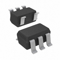
DBV PACKAGE
(TOP VIEW)
Output Swing Includes Both Supply Rails
Low Noise . . . 19 nV/√Hz Typ at f = 1 kHz
Low Input Bias Current . . . 1 pA Typ
Fully Specified for Single-Supply 3-V and
5-V Operation
Very Low Power . . . 110 µA Typ
Common-Mode Input Voltage Range
Includes Negative Rail
Wide Supply Voltage Range
2.7 V to 10 V
Macromodel Included
OUT
1
VDD+
2
IN +
3
5
VDD− /GND
4
IN−
description
The TLV2721 is a single low-voltage operational amplifier available in the SOT-23 package. It offers a
compromise between the ac performance and output drive of the TLV2731 and the micropower TLV2711.
It consumes only 150 µA (max) of supply current and is ideal for battery-powered applications. The device
exhibits rail-to-rail output performance for increased dynamic range in single- or split-supply applications. The
TLV2721 is fully characterized at 3 V and 5 V and is optimized for low-voltage applications.
The TLV2721, exhibiting high input impedance and low noise, is excellent for small-signal conditioning for
high-impedance sources, such as piezoelectric transducers. Because of the micropower dissipation levels
combined with 3-V operation, these devices work well in hand-held monitoring and remote-sensing
applications. In addition, the rail-to-rail output feature with single or split supplies makes this family a great
choice when interfacing with analog-to-digital converters (ADCs).
With a total area of 5.6mm2, the SOT-23 package only requires one third the board space of the standard 8-pin
SOIC package. This ultra-small package allows designers to place single amplifiers very close to the signal
source, minimizing noise pick-up from long PCB traces.
AVAILABLE OPTIONS
PACKAGED DEVICES
TA
VIOmax AT 25°C
0°C to 70°C
3 mV
TLV2721CDBV
VAKC
−40°C to 85°C
3 mV
TLV2721IDBV
VAKI
SOT-23 (DBV)†
SYMBOL
CHIP
FORM‡
(Y)
TLV2721Y
† The DBV package available in tape and reel only.
‡ Chip forms are tested at TA = 25°C only.
Please be aware that an important notice concerning availability, standard warranty, and use in critical applications of
Texas Instruments semiconductor products and disclaimers thereto appears at the end of this data sheet.
Advanced LinCMOS is a trademark of Texas Instruments.
Copyright 2001, Texas Instruments Incorporated
���������� � � �
!"#$�%�"
�& �'##�
% �& "! (')*���%�"
�%�+
�#"
'�%& �"
!"#$ %" &(���!���%�"
& (�# %,� %�#$& "! ��-�& �
&%#'$�
%&
&%�
�#
.�##�
%/+ �#"
'�%�"
(#"��&&�
0
"�&
"%
���&&�#�*/ �
�*'
�
%�&%�
0 "! �** (�#�$�%�#&+
POST OFFICE BOX 655303
• DALLAS, TEXAS 75265
1
��������� ��������
��
��
��
���� � ������� ��
���� ��������� ������ ���� ���� � ���������
SLOS197A − AUGUST1997 − REVISED MARCH 2001
TLV2721Y chip information
This chip, when properly assembled, displays characteristics similar to the TLV2721C. Thermal compression
or ultrasonic bonding may be used on the doped-aluminum bonding pads. This chip may be mounted with
conductive epoxy or a gold-silicon preform.
BONDING PAD ASSIGNMENTS
(5)
VDD +
(2)
(1)
(3)
+
IN +
(4)
(1)
OUT
−
IN −
(5)
VDD − / GND
CHIP THICKNESS: 10 MILS TYPICAL
BONDING PADS: 4 × 4 MILS MINIMUM
46
(2)
TJmax = 150°C
TOLERANCES ARE ± 10%.
ALL DIMENSIONS ARE IN MILS.
PIN (2) IS INTERNALLY CONNECTED
TO BACKSIDE OF CHIP.
(4)
(3)
31
2
POST OFFICE BOX 655303
• DALLAS, TEXAS 75265
��������� ��������
��
��
��
���� � ������� ��
���� ��������� ������ ���� ���� � ���������
SLOS197A − AUGUST1997 − REVISED MARCH 2001
equivalent schematic
VDD +
Q3
Q6
Q9
R7
IN +
Q12
Q14
Q16
C2
R6
OUT
C1
IN −
R5
Q1
Q4
Q13
Q15
R2
Q2
Q5
R3
R4
Q7
Q8
Q10
Q17
D1
Q11
R1
VDD −/ GND
COMPONENT COUNT†
Transistors
Diodes
Resistors
Capacitors
23
5
11
2
† Includes both amplifiers and all
ESD, bias, and trim circuitry
POST OFFICE BOX 655303
• DALLAS, TEXAS 75265
3
��������� ��������
��
��
��
���� � ������� ��
���� ��������� ������ ���� ���� � ���������
SLOS197A − AUGUST1997 − REVISED MARCH 2001
absolute maximum ratings over operating free-air temperature range (unless otherwise noted)†
Supply voltage, VDD (see Note 1) . . . . . . . . . . . . . . . . . . . . . . . . . . . . . . . . . . . . . . . . . . . . . . . . . . . . . . . . . . . . 12 V
Differential input voltage, VID (see Note 2) . . . . . . . . . . . . . . . . . . . . . . . . . . . . . . . . . . . . . . . . . . . . . . . . . . . ± VDD
Input voltage range, VI (any input, see Note 1) . . . . . . . . . . . . . . . . . . . . . . . . . . . . . . . . . . . . . . . . −0.3 V to VDD
Input current, II (each input) . . . . . . . . . . . . . . . . . . . . . . . . . . . . . . . . . . . . . . . . . . . . . . . . . . . . . . . . . . . . . . . ± 5 mA
Output current, IO . . . . . . . . . . . . . . . . . . . . . . . . . . . . . . . . . . . . . . . . . . . . . . . . . . . . . . . . . . . . . . . . . . . . . . . ± 50 mA
Total current into VDD + . . . . . . . . . . . . . . . . . . . . . . . . . . . . . . . . . . . . . . . . . . . . . . . . . . . . . . . . . . . . . . . . . . ± 50 mA
Total current out of VDD − . . . . . . . . . . . . . . . . . . . . . . . . . . . . . . . . . . . . . . . . . . . . . . . . . . . . . . . . . . . . . . . . ± 50 mA
Duration of short-circuit current (at or below) 25°C (see Note 3) . . . . . . . . . . . . . . . . . . . . . . . . . . . . . . unlimited
Continuous total power dissipation . . . . . . . . . . . . . . . . . . . . . . . . . . . . . . . . . . . . . See Dissipation Rating Table
Operating free-air temperature range, TA: TLV2721C . . . . . . . . . . . . . . . . . . . . . . . . . . . . . . . . . . . 0°C to 70°C
TLV2721I . . . . . . . . . . . . . . . . . . . . . . . . . . . . . . . . . . −40°C to 85°C
Storage temperature range, Tstg . . . . . . . . . . . . . . . . . . . . . . . . . . . . . . . . . . . . . . . . . . . . . . . . . . . −65°C to 150°C
Lead temperature 1,6 mm (1/16 inch) from case for 10 seconds: DBV package . . . . . . . . . . . . . . . . . . 260°C
† Stresses beyond those listed under “absolute maximum ratings” may cause permanent damage to the device. These are stress ratings only, and
functional operation of the device at these or any other conditions beyond those indicated under “recommended operating conditions” is not
implied. Exposure to absolute-maximum-rated conditions for extended periods may affect device reliability.
NOTES: 1. All voltage values, except differential voltages, are with respect to VDD − .
2. Differential voltages are at the noninverting input with respect to the inverting input. Excessive current flows when input is brought
below VDD − − 0.3 V.
3. The output can be shorted to either supply. Temperature and /or supply voltages must be limited to ensure that the maximum
dissipation rating is not exceeded.
DISSIPATION RATING TABLE
PACKAGE
TA ≤ 25°C
25 C
POWER RATING
DERATING FACTOR
ABOVE TA = 25°C
70°C
TA = 70
C
POWER RATING
85°C
TA = 85
C
POWER RATING
DBV
150 mW
1.2 mW/°C
96 mW
78 mW
recommended operating conditions
TLV2721C
MIN
Supply voltage, VDD ���� ���� ��
2.7
Input voltage range, VI
VDD −
VDD −
Common-mode input voltage, VIC
Operating free-air temperature, TA
NOTE 1: All voltage values, except differential voltages, are with respect to VDD − .
4
POST OFFICE BOX 655303
0
• DALLAS, TEXAS 75265
MAX
10
VDD + − 1.3
VDD + − 1.3
70
TLV2721I
MIN
2.7
VDD −
VDD −
−40
MAX
10
VDD + − 1.3
VDD + − 1.3
85
UNIT
V
V
V
°C
��������� ��������
��
��
��
���� � ������� ��
���� ��������� ������ ���� ���� � ���������
SLOS197A − AUGUST1997 − REVISED MARCH 2001
electrical characteristics at specified free-air temperature, VDD = 3 V (unless otherwise noted)
PARAMETER
VIO
Input offset voltage
αVIO
Temperature
coefficient of input
offset voltage
Input offset voltage
long-term drift
(see Note 4)
IIO
Input offset current
IIB
Input bias current
VICR
Common-mode input
voltage range
TA†
TEST CONDITIONS
TLV2721C
MIN
Full range
VDD ± = ± 1.5 V,
VO = 0,
VIC = 0,
RS = 50 Ω
VOH
VOL
AVD
Low-level output
voltage
Large-signal
differential voltage
amplification
0.5
3
3
mV
0.003
0.003
µV/mo
25°C
0.5
Full range
60
0.5
150
1
60
1
150
0 to 2
−0.3
to 2.2
−0.3
to 2.2
2.97
2.97
2.88
2.88
2.6
pA
V
0 to
1.7
25°C
pA
60
150
0 to 2
0 to
1.7
60
150
25°C
Full range
IOL = 50 µA
0.5
UNIT
25°C
|VIO| ≤ 5 mV
VIC = 1.5 V,
MAX
µV/°C
V/°C
25°C
IOH = − 400 µA
A
TYP
1
Full range
IOH = − 100 µA
MIN
1
25°C
High-level output
voltage
MAX
Full range
RS = 50 Ω
Ω,,
TLV2721I
TYP
V
2.6
25°C
15
15
25°C
150
150
VIC = 1.5 V,
IOL = 500 µA
A
RL = 2 kه
25°C
2
VIC = 1.5 V,
VO = 1 V to 2 V
Full range
1
RL = 1 Mه
25°C
250
250
Full range
500
3
mV
500
2
3
1
V/mV
rid
Differential input
resistance
25°C
1012
1012
Ω
ric
Common-mode input
resistance
25°C
1012
1012
Ω
cic
Common-mode input
capacitance
f = 10 kHz
25°C
6
6
pF
zo
Closed-loop output
impedance
f = 10 kHz,
25°C
90
90
Ω
CMRR
Common-mode
rejection ratio
VIC = 0 to 1.7 V,
VO = 1.5 V,
RS = 50 Ω
kSVR
Supply voltage
rejection ratio
(∆VDD /∆VIO)
VDD = 2.7 V to 8 V,
VIC = VDD /2,
No load
IDD
Supply current
VO = 1.5 V,
AV = 10
No load
25°C
70
Full range
65
25°C
80
Full range
80
82
70
82
dB
65
95
80
95
dB
25°C
Full range
80
100
150
200
100
150
200
µA
† Full range for the TLV2721C is 0°C to 70°C. Full range for the TLV2721I is − 40°C to 85°C.
‡ Referenced to 1.5 V
NOTE 4: Typical values are based on the input offset voltage shift observed through 500 hours of operating life test at TA = 150°C extrapolated
to TA = 25°C using the Arrhenius equation and assuming an activation energy of 0.96 eV.
POST OFFICE BOX 655303
• DALLAS, TEXAS 75265
5
��������� ��������
��
��
��
���� � ������� ��
���� ��������� ������ ���� ���� � ���������
SLOS197A − AUGUST1997 − REVISED MARCH 2001
operating characteristics at specified free-air temperature, VDD = 3 V
PARAMETER
TEST CONDITIONS
RL = 2 kه,
TLV2721C
TA†
MIN
TYP
25°C
0.1
0.25
Full
range
0.05
TLV2721I
MAX
MIN
TYP
0.1
0.25
SR
Slew rate at unity
gain
VO = 1.1 V to 1.9 V,
CL = 100 pF‡
Equivalent input
noise voltage
f = 10 Hz
25°C
120
120
Vn
f = 1 kHz
25°C
20
20
Peak-to-peak
equivalent input
noise voltage
f = 0.1 Hz to 1 Hz
25°C
680
680
VN(PP)
f = 0.1 Hz to 10 Hz
25°C
860
860
In
Equivalent input
noise current
25°C
0.6
0.6
2.52%
2.52%
7.01%
7.01%
0.076%
0.076%
0.147%
0.147%
AV = 1
VO = 1 V to 2 V,
f = 20 kHz,
RL = 2 k٧
AV = 1
Gain-bandwidth
product
f = 1 kHz,
CL = 100 pF‡
RL = 2 kه,
BOM
Maximum
output-swing
bandwidth
VO(PP) = 1 V,
RL = 2 kه,
ts
Settling time
φm
Total harmonic
distortion plus noise
Phase margin at
unity gain
V/µs
0.05
nV/√Hz
fA /√Hz
25°C
AV = 10
25°C
AV = 10
25°C
480
480
kHz
AV = 1,
CL = 100 pF‡
25°C
30
30
kHz
AV = −1,
Step = 1 V to 2 V,
RL = 2 kه,
CL = 100 pF‡
To 0.1%
25°C
4.5
4.5
µs
To 0.01%
25°C
6.8
6.8
µs
RL = 2 kه,
CL = 100 pF‡
25°C
53°
53°
25°C
12
12
Gain margin
† Full range is − 40°C to 85°C.
‡ Referenced to 1.5 V
§ Referenced to 0 V
6
UNIT
mV
VO = 1 V to 2 V,
f = 20 kHz,
RL = 2 kه
THD+N
MAX
POST OFFICE BOX 655303
• DALLAS, TEXAS 75265
dB
��������� ��������
��
��
��
���� � ������� ��
���� ��������� ������ ���� ���� � ���������
SLOS197A − AUGUST1997 − REVISED MARCH 2001
electrical characteristics at specified free-air temperature, VDD = 5 V (unless otherwise noted)
PARAMETER
VIO
Input offset voltage
αVIO
Temperature
coefficient of input
offset voltage
Input offset voltage
long-term drift
(see Note 4)
TA†
TEST CONDITIONS
TLV2721C
MIN
Full range
VDD ± = ± 2.5 V,
VO = 0,
VIC = 0,
RS = 50 Ω
TLV2721I
TYP
MAX
0.5
3
MIN
TYP
MAX
0.5
3
1
µV/°C
V/°C
25°C
0.003
0.003
µV/mo
25°C
0.5
60
0.5
Input offset current
IIB
Input bias current
VICR
Common-mode input
voltage range
RS = 50 Ω,
Ω
VOH
High-level output
voltage
IOL = 50 µA
25°C
12
VOL
Low-level output
voltage
IOH = − 500 µA
IOH = − 1 mA
VIC = 2.5 V,
A
IOL = 500 µA
25°C
120
VIC = 2.5 V,
Full range
RL = 2 kه
25°C
3
VIC = 2.5 V,
VO = 1 V to 4 V
Full range
1
RL = 1 Mه
25°C
800
800
Full range
150
25°C
AVD
mV
1
IIO
Large-signal
differential voltage
amplification
UNIT
1
Full range
25°C
|VIO| ≤ 5 mV
Full range
25°C
60
1
150
0 to 4
−0.3
to 4.2
pA
60
150
0 to 4
0 to
3.5
60
150
pA
−0.3
to 4.2
V
0 to
3.5
4.75
4.88
4.75
4.88
4.6
4.76
4.6
4.76
V
12
120
500
5
mV
500
3
5
1
V/mV
rid
Differential input
resistance
25°C
1012
1012
Ω
ric
Common-mode
input resistance
25°C
1012
1012
Ω
cic
Common-mode
input capacitance
f = 10 kHz
25°C
6
6
pF
zo
Closed-loop
output impedance
f = 10 kHz,
AV = 10
25°C
70
70
Ω
CMRR
Common-mode
rejection ratio
VIC = 0 to 2.7 V,
RS = 50 Ω
VO = 1.5 V,
kSVR
Supply voltage
rejection ratio
(∆VDD /∆VIO)
VDD = 4.4 V to 8 V,
VIC = VDD /2,
No load
IDD
Supply current
VO = 2.5 V,
No load
25°C
70
Full range
65
25°C
80
Full range
80
85
70
85
dB
65
95
80
95
dB
25°C
Full range
80
110
150
200
110
150
200
µA
† Full range for the TLV2721C is 0°C to 70°C. Full range for the TLV2721I is − 40°C to 85°C.
‡ Referenced to 2.5 V
NOTE 5: Typical values are based on the input offset voltage shift observed through 500 hours of operating life test at TA = 150°C extrapolated
to TA = 25°C using the Arrhenius equation and assuming an activation energy of 0.96 eV.
POST OFFICE BOX 655303
• DALLAS, TEXAS 75265
7
��������� ��������
��
��
��
���� � ������� ��
���� ��������� ������ ���� ���� � ���������
SLOS197A − AUGUST1997 − REVISED MARCH 2001
operating characteristics at specified free-air temperature, VDD = 5 V
PARAMETER
TEST CONDITIONS
RL = 2 kه,
TLV2721C
TA†
MIN
TYP
25°C
0.1
0.25
Full
range
0.05
TLV2721I
MAX
MIN
TYP
0.1
0.25
SR
Slew rate at unity
gain
VO = 1.5 V to 3.5 V,
CL = 100 pF‡
Equivalent input
noise voltage
f = 10 Hz
25°C
90
90
Vn
f = 1 kHz
25°C
19
19
Peak-to-peak
equivalent input
noise voltage
f = 0.1 Hz to 1 Hz
25°C
800
800
VN(PP)
f = 0.1 Hz to 10 Hz
25°C
960
960
In
Equivalent input
noise current
25°C
0.6
0.6
2.45%
2.45%
5.54%
5.54%
0.142%
0.142%
0.257%
0.257%
THD+N
BOM
ts
φm
AV = 1
VO = 1.5 V to 3.5 V,
f = 20 kHz,
RL = 2 k٧
AV = 1
Gain-bandwidth
product
f = 1 kHz,
CL = 100 pF‡
RL = 2 kه,
Maximum outputswing bandwidth
VO(PP) = 1 V,
RL = 2 kه,
Settling time
Phase margin at
unity gain
V/µs
0.05
nV/√Hz
fA /√Hz
25°C
AV = 10
25°C
AV = 10
25°C
510
510
kHz
AV = 1,
CL = 100 pF‡
25°C
40
40
kHz
AV = −1,
Step = 1.5 V to 3.5 V,
RL = 2 kه,
CL = 100 pF‡
To 0.1%
25°C
6.8
6.8
To 0.01%
25°C
9.2
9.2
RL = 2 kه,
CL = 100 pF‡
25°C
53°
53°
25°C
12
12
µss
Gain margin
† Full range is − 40°C to 85°C.
‡ Referenced to 2.5 V
§ Referenced to 0 V
8
UNIT
mV
VO = 1.5 V to 3.5 V,
f = 20 kHz,
RL = 2 kه
Total harmonic
distortion plus noise
MAX
POST OFFICE BOX 655303
• DALLAS, TEXAS 75265
dB
��������� ��������
��
��
��
���� � ������� ��
���� ��������� ������ ���� ���� � ���������
SLOS197A − AUGUST1997 − REVISED MARCH 2001
electrical characteristics at VDD = 3 V, TA = 25°C (unless otherwise noted)
PARAMETER
VIO
IIO
Input offset voltage
IIB
Input bias current
VICR
VOH
TLV2721Y
TEST CONDITIONS
VIC = 0,
Common-mode input voltage range
| VIO| ≤ 5 mV,
RS = 50 Ω
High-level output voltage
IOH = − 100 µA
VIC = 1.5 V,
VOL
Low-level output voltage
AVD
Large-signal differential
voltage amplification
rid
Differential input resistance
ric
Common-mode input resistance
cic
Common-mode input capacitance
f = 10 kHz
zo
Closed-loop output impedance
f = 10 kHz,
CMRR
Common-mode rejection ratio
kSVR
Supply voltage rejection ratio (∆VDD /∆VIO)
VIC = 0 to 1.7 V,
VDD = 2.7 V to 8 V,
VIC = 1.5 V,
VO = 1 V to 2 V
IDD
Supply current
† Referenced to 1.5 V
VO = 0,
TYP
MAX
VO = 0,
IOL = 50 µA
IOL = 500 µA
UNIT
µV
620
VDD ± = ± 1.5 V,
RS = 50 Ω
Input offset current
MIN
0.5
60
pA
1
60
pA
−0.3
to 2.2
V
2.97
V
15
mV
150
RL = 2 kن
3
RL = 1 Mن
V/mV
250
AV = 10
VO = 0,
RS = 50 Ω
VIC = 0,
No load
No load
1012
1012
Ω
6
pF
Ω
90
Ω
82
dB
95
dB
100
µA
electrical characteristics at VDD = 5 V, TA = 25°C (unless otherwise noted)
PARAMETER
VIO
IIO
Input offset voltage
IIB
Input bias current
VICR
VIC = 0,
Common-mode input voltage range
| VIO| ≤ 5 mV,
RS = 50 Ω
VOH
High-level output voltage
VOL
Low-level output voltage
IOH = − 500 µA
VIC = 2.5 V,
AVD
Large-signal differential
voltage amplification
rid
Differential input resistance
ric
Common-mode input resistance
cic
Common-mode input capacitance
f = 10 kHz
zo
Closed-loop output impedance
f = 10 kHz,
CMRR
Common-mode rejection ratio
kSVR
Supply voltage rejection ratio (∆VDD /∆VIO)
VIC = 0 to 1.7 V,
VDD = 2.7 V to 8 V,
VIC = 2.5 V,
VO = 1 V to 4 V
VO = 0,
POST OFFICE BOX 655303
MIN
TYP
MAX
VO = 0,
IOL = 50 µA
IOL = 500 µA
RL = 2 kن
60
pA
1
60
pA
−0.3
to 4.2
V
4.88
V
12
120
800
AV = 10
VO = 0,
RS = 50 Ω
VIC = 0,
No load
• DALLAS, TEXAS 75265
0.5
mV
5
RL = 1 Mن
No load
UNIT
µV
610
VDD ± = ± 1.5 V,
RS = 50 Ω
Input offset current
IDD
Supply current
† Referenced to 2.5 V
TLV2721Y
TEST CONDITIONS
V/mV
1012
1012
Ω
6
pF
Ω
70
Ω
85
dB
95
dB
110
µA
9
��������� ��������
��
��
��
���� � ������� ��
���� ��������� ������ ���� ���� � ���������
SLOS197A − AUGUST1997 − REVISED MARCH 2001
TYPICAL CHARACTERISTICS
Table of Graphs
FIGURE
VIO
Input offset voltage
Distribution
vs Common-mode input voltage
1, 2
3, 4
αVIO
IIB/IIO
Input offset voltage temperature coefficient
Distribution
5, 6
Input bias and input offset currents
vs Free-air temperature
7
VI
Input voltage
vs Supply voltage
vs Free-air temperature
8
9
VOH
VOL
High-level output voltage
vs High-level output current
10, 13
Low-level output voltage
vs Low-level output current
11, 12, 14
VO(PP)
Maximum peak-to-peak output voltage
vs Frequency
15
IOS
Short-circuit output current
vs Supply voltage
vs Free-air temperature
16
17
VO
AVD
Output voltage
vs Differential input voltage
Differential voltage amplification
vs Load resistance
AVD
Large signal differential voltage amplification
vs Frequency
vs Free-air temperature
21, 22
23, 24
zo
Output impedance
vs Frequency
25, 26
CMRR
Common-mode rejection ratio
vs Frequency
vs Free-air temperature
27
28
kSVR
Supply-voltage rejection ratio
vs Frequency
vs Free-air temperature
29, 30
31
IDD
Supply current
vs Supply voltage
32
SR
Slew rate
vs Load capacitance
vs Free-air temperature
33
34
VO
VO
Inverting large-signal pulse response
35, 36
Voltage-follower large-signal pulse response
37, 38
VO
VO
Inverting small-signal pulse response
39, 40
Vn
Equivalent input noise voltage
vs Frequency
Input noise voltage (referred to input)
Over a 10-second period
45
Total harmonic distortion plus noise
vs Frequency
46
Gain-bandwidth product
vs Free-air temperature
vs Supply voltage
47
48
Phase margin
vs Frequency
vs Load capacitance
21, 22
51, 52
Gain margin
vs Load capacitance
49, 50
Unity-gain bandwidth
vs Load capacitance
53, 54
THD + N
φm
B1
10
Voltage-follower small-signal pulse response
POST OFFICE BOX 655303
18, 19
20
41, 42
• DALLAS, TEXAS 75265
43, 44
��������� ��������
��
��
��
���� � ������� ��
���� ��������� ������ ���� ���� � ���������
SLOS197A − AUGUST1997 − REVISED MARCH 2001
TYPICAL CHARACTERISTICS
DISTRIBUTION OF TLV2721
INPUT OFFSET VOLTAGE
DISTRIBUTION OF TLV2721
INPUT OFFSET VOLTAGE
25
20
18
Precentage of Amplifiers − %
16
Precentage of Amplifiers − %
545 Amplifiers
From 1 Wafer Lot
VDD = ± 1.5 V
TA = 25°C
14
12
10
8
6
4
545 Amplifiers From 1 Wafer Lot
VDD = ± 2.5 V
TA = 25°C
20
15
10
5
2
0
0
−1.5
−1.1
−0.7
−0.3
0.1
0.5
0.9
−1.5
1.3
VIO − Input Offset Voltage − mV
−1.1 −0.7 −0.3
0.1
0.5
0.9
VIO − Input Offset Voltage − mV
Figure 1
Figure 2
INPUT OFFSET VOLTAGE†
vs
COMMON-MODE INPUT VOLTAGE
INPUT OFFSET VOLTAGE†
vs
COMMON-MODE INPUT VOLTAGE
1
0.8
1
VDD = 3 V
RS = 50 Ω
TA = 25°C
0.8
VIO − Input Offset Voltage − mV
VIO − Input Offset Voltage − mV
0.6
0.4
0.2
0
−0.2
ÁÁ
ÁÁ
VDD = 5 V
RS = 50 Ω
TA = 25°C
0.6
0.4
0.2
0
−0.2
ÁÁ
ÁÁ
−0.4
−0.6
−0.8
−1
−1
1.3
−0.4
−0.6
−0.8
0
1
2
3
VIC − Common-Mode Input Voltage − V
−1
−1
3
4
0
1
2
VIC − Common-Mode Input Voltage − V
Figure 3
5
Figure 4
† For all curves where VDD = 5 V, all loads are referenced to 2.5 V. For all curves where VDD = 3 V, all loads are referenced to 1.5 V.
POST OFFICE BOX 655303
• DALLAS, TEXAS 75265
11
��������� ��������
��
��
��
���� � ������� ��
���� ��������� ������ ���� ���� � ���������
SLOS197A − AUGUST1997 − REVISED MARCH 2001
TYPICAL CHARACTERISTICS
DISTRIBUTION OF TLV2721 INPUT OFFSET
VOLTAGE TEMPERATURE COEFFICIENT†
DISTRIBUTION OF TLV2721 INPUT OFFSET
VOLTAGE TEMPERATURE COEFFICIENT†
25
32 Amplifiers From 1 Wafer Lot
VDD = ± 1.5 V
P Package
TA = 25°C to 125°C
20
Percentage of Amplifiers − %
Percentage of Amplifiers − %
25
15
10
5
0
−4
−3
−2
−1
0
1
2
3
20
15
10
5
0
4
32 Amplifiers From 1 Wafer Lot
VDD = ± 2.5 V
P Package
TA = 25°C to 125°C
−4
−3
α VIO − Input Offset Voltage
Temperature Coefficient − µV/°C
−2
3
4
2
2.5
3
3.5
|VDD ±| − Supply Voltage − V
4
5
VDD± = ± 2.5 V
VIC = 0
VO = 0
RS = 50 Ω
RS = 50 Ω
TA = 25°C
4
3
70
VI − Input Voltage − V
IIIB
IB and IIIO
IO − Input Bias and Input Offset Currents − pA
2
INPUT VOLTAGE
vs
SUPPLY VOLTAGE
100
60
50
ÁÁ
ÁÁ
40
30
IIB
20
2
1
0
|VIO| ≤ 5 mV
−1
−2
−3
−4
10
0
25
1
Figure 6
INPUT BIAS AND INPUT OFFSET CURRENTS
vs
FREE-AIR TEMPERATURE
80
0
α VIO − Input Offset Voltage
Temperature Coefficient − µV/°C
Figure 5
90
−1
IIO
−5
105
45
65
85
TA − Free-Air Temperature − °C
125
1
Figure 7
1.5
Figure 8
† Data at high and low temperatures are applicable only within the rated operating free-air temperature ranges of the various devices.
12
POST OFFICE BOX 655303
• DALLAS, TEXAS 75265
��������� ��������
��
��
��
���� � ������� ��
���� ��������� ������ ���� ���� � ���������
SLOS197A − AUGUST1997 − REVISED MARCH 2001
TYPICAL CHARACTERISTICS
INPUT VOLTAGE†‡
vs
FREE-AIR TEMPERATURE
HIGH-LEVEL OUTPUT VOLTAGE†‡
vs
HIGH-LEVEL OUTPUT CURRENT
3
5
VDD = 3 V
VDD = 5 V
2.5
VOH − High-Level Output Voltage − V
4
VI − Input Voltage − V
3
|VIO| ≤ 5 mV
2
ÁÁ
1
0
−1
−55 −35 −15
5
25
45
65 85 105
TA − Free-Air Temperature − °C
125
TA = − 40°C
2
TA = 25°C
1.5
TA = 85°C
1
ÁÁ
ÁÁ
ÁÁ
TA = 125°C
0.5
0
0
0.5 1
1.5 2 2.5 3 3.5 4 4.5
|IOH| − High-Level Output Current − mA
Figure 9
Figure 10
LOW-LEVEL OUTPUT VOLTAGE‡
vs
LOW-LEVEL OUTPUT CURRENT
LOW-LEVEL OUTPUT VOLTAGE†‡
vs
LOW-LEVEL OUTPUT CURRENT
1.4
VDD = 3 V
TA = 25°C
1
VOL − Low-Level Output Voltage − V
VOL − Low-Level Output Voltage − V
1.2
VIC = 0
0.8
VIC = 1.5 V
VIC = 0.75 V
0.6
0.4
ÁÁ
ÁÁ
5
VDD = 3 V
VIC = 1.5 V
1.2
TA = 125°C
1
TA = 85°C
0.8
0.6
TA = 25°C
ÁÁ
ÁÁ
0.2
0
0.4
TA = − 40°C
0.2
0
0
1
2
3
4
5
IOL − Low-Level Output Current − mA
0
1
2
3
4
5
IOL − Low-Level Output Current − mA
Figure 11
Figure 12
† Data at high and low temperatures are applicable only within the rated operating free-air temperature ranges of the various devices.
‡ For all curves where VDD = 5 V, all loads are referenced to 2.5 V. For all curves where VDD = 3 V, all loads are referenced to 1.5 V.
POST OFFICE BOX 655303
• DALLAS, TEXAS 75265
13
��������� ��������
��
��
��
���� � ������� ��
���� ��������� ������ ���� ���� � ���������
SLOS197A − AUGUST1997 − REVISED MARCH 2001
TYPICAL CHARACTERISTICS
LOW-LEVEL OUTPUT VOLTAGE†‡
vs
LOW-LEVEL OUTPUT CURRENT
HIGH-LEVEL OUTPUT VOLTAGE†‡
vs
HIGH-LEVEL OUTPUT CURRENT
1.4
5
ÁÁ
ÁÁ
4
TA = − 40°C
TA = 25°C
3
TA = 85°C
2
TA = 125°C
ÁÁ
ÁÁ
1
0
0
1
2
3
4
5
6
7
VDD = 5 V
VIC = 2.5 V
1.2
VOL − Low-Level Output Voltage − V
VOH − High-Level Output Voltage − V
VDD = 5 V
VIC = 2.5 V
TA = 125°C
1
TA = 85°C
0.8
0.6
TA = 25°C
0.4
TA = − 40°C
0.2
0
0
8
1
2
|IOH| − High-Level Output Current − mA
Figure 13
20
5
VDD = 5 V
4
3
VDD = 3 V
2
1
RL = 2 kΩ
TA = 25°C
0
10 2
VO = VDD/2
TA = 25°C
VIC = VDD/2
16
VID = − 100 mV
12
8
4
0
VID = 100 mV
−4
−8
10 3
10 4
f − Frequency − Hz
10 5
2
Figure 15
3
4
5
6
VDD − Supply Voltage − V
7
Figure 16
† Data at high and low temperatures are applicable only within the rated operating free-air temperature ranges of the various devices.
‡ For all curves where VDD = 5 V, all loads are referenced to 2.5 V. For all curves where VDD = 3 V, all loads are referenced to 1.5 V.
14
6
SHORT-CIRCUIT OUTPUT CURRENT
vs
SUPPLY VOLTAGE
I OS − Short-Circuit Output Current − mA
VO(PP) − Maximum Peak-to-Peak Output Voltage − V
5
Figure 14
MAXIMUM PEAK-TO-PEAK OUTPUT VOLTAGE‡
vs
FREQUENCY
ÁÁ
ÁÁ
ÁÁ
4
3
IOL − Low-Level Output Current − mA
POST OFFICE BOX 655303
• DALLAS, TEXAS 75265
8
��������� ��������
��
��
��
���� � ������� ��
���� ��������� ������ ���� ���� � ���������
SLOS197A − AUGUST1997 − REVISED MARCH 2001
TYPICAL CHARACTERISTICS
SHORT-CIRCUIT OUTPUT CURRENT †‡
vs
FREE-AIR TEMPERATURE
OUTPUT VOLTAGE‡
vs
DIFFERENTIAL INPUT VOLTAGE
3
VDD = 5 V
VIC = 2.5 V
VO = 2.5 V
16
12
VID = − 100 mV
8
4
0
VID = 100 mV
2
1.5
1
0.5
−4
−8
−75
VDD = 3 V
RI = 2 kΩ
VIC = 1.5 V
TA = 25°C
2.5
V O − Output Voltage − V
I OS − Short-Circuit Output Current − mA
20
0
−50
−25
0
25
50
75
100
TA − Free-Air Temperature − °C
−5
125
−4
−3 −2 −1 0
1
2
3
VID − Differential Input Voltage − V
Figure 17
DIFFERENTIAL VOLTAGE AMPLIFICATION‡
vs
LOAD RESISTANCE
AVD − Differential Voltage Amplification − V/mV
V O − Output Voltage − V
4
VDD = 5 V
VIC = 2.5 V
RL = 2 kΩ
TA = 25°C
3
2
1
0
10 3
VO(PP) = 2 V
TA = 25°C
−3
−2
−1
0
1
2
3
4
5
VID − Differential Input Voltage − V
VDD = 5 V
10 2
VDD = 3 V
10 1
ÁÁ
ÁÁ
ÁÁ
1
−5 −4
5
Figure 18
OUTPUT VOLTAGE‡
vs
DIFFERENTIAL INPUT VOLTAGE
5
4
1
Figure 19
101
10 2
10 3
RL − Load Resistance − kΩ
Figure 20
† Data at high and low temperatures are applicable only within the rated operating free-air temperature ranges of the various devices.
‡ For all curves where VDD = 5 V, all loads are referenced to 2.5 V. For all curves where VDD = 3 V, all loads are referenced to 1.5 V.
POST OFFICE BOX 655303
• DALLAS, TEXAS 75265
15
��������� ��������
��
��
��
���� � ������� ��
���� ��������� ������ ���� ���� � ���������
SLOS197A − AUGUST1997 − REVISED MARCH 2001
TYPICAL CHARACTERISTICS
LARGE-SIGNAL DIFFERENTIAL VOLTAGE†
AMPLIFICATION AND PHASE MARGIN
vs
FREQUENCY
ÁÁ
ÁÁ
60
180°
VDD = 5 V
RL = 2 kΩ
CL= 100 pF
TA = 25°C
135°
90°
40
Phase Margin
45°
20
Gain
0
0°
φom
m − Phase Margin
AVD
A
VD − Large-Signal Differential
Voltage Amplification − dB
80
−45°
−20
−40
104
105
106
f − Frequency − Hz
−90°
107
Figure 21
LARGE-SIGNAL DIFFERENTIAL VOLTAGE
AMPLIFICATION AND PHASE MARGIN†
vs
FREQUENCY
ÁÁ
ÁÁ
60
180°
VDD = 3 V
RL = 2 kΩ
CL= 100 pF
TA = 25°C
135°
90°
40
Phase Margin
45°
20
0
Gain
0°
−45°
−20
−40
104
φom
m − Phase Margin
AVD
A
VD − Large-Signal Differential
Voltage Amplification − dB
80
105
106
f − Frequency − Hz
−90°
107
Figure 22
† For all curves where VDD = 5 V, all loads are referenced to 2.5 V. For all curves where VDD = 3 V, all loads are referenced to 1.5 V.
16
POST OFFICE BOX 655303
• DALLAS, TEXAS 75265
��������� ��������
��
��
��
���� � ������� ��
���� ��������� ������ ���� ���� � ���������
SLOS197A − AUGUST1997 − REVISED MARCH 2001
TYPICAL CHARACTERISTICS
LARGE-SIGNAL DIFFERENTIAL
VOLTAGE AMPLIFICATION†‡
vs
FREE-AIR TEMPERATURE
LARGE-SIGNAL DIFFERENTIAL
VOLTAGE AMPLIFICATION†‡
vs
FREE-AIR TEMPERATURE
10 4
VDD = 3 V
VIC = 1.5 V
VO = 0.5 V to 2.5 V
AVD − Large-Signal Differential Voltage
Amplification − V/mV
AVD − Large-Signal Differential Voltage
Amplification − V/mV
10 3
RL = 1 MΩ
10 2
10 1
RL = 2 kΩ
1
−75
−50
−25
0
25
50
75
100
TA − Free-Air Temperature − °C
VDD = 5 V
VIC = 2.5 V
VO = 1 V to 4 V
10 2
10 1
1
−75
125
RL = 2 kΩ
−50
−25
0
25
50
75
100
TA − Free-Air Temperature − °C
Figure 23
OUTPUT IMPEDANCE‡
vs
FREQUENCY
1000
1000
VDD = 5 V
TA = 25°C
z o − Output Impedance − Ω
z o − Output Impedance − Ω
VDD = 3 V
TA = 25°C
100
AV = 100
1
101
125
Figure 24
OUTPUT IMPEDANCE‡
vs
FREQUENCY
10
RL = 1 MΩ
10 3
AV = 10
100
AV = 100
10
AV = 10
1
AV = 1
AV = 1
10 2
10 3
f− Frequency − Hz
10 4
10 5
0.1
10 1
Figure 25
10 2
10 3
f− Frequency − Hz
10 4
10 5
Figure 26
† Data at high and low temperatures are applicable only within the rated operating free-air temperature ranges of the various devices.
‡ For all curves where VDD = 5 V, all loads are referenced to 2.5 V. For all curves where VDD = 3 V, all loads are referenced to 1.5 V.
POST OFFICE BOX 655303
• DALLAS, TEXAS 75265
17
��������� ��������
��
��
��
���� � ������� ��
���� ��������� ������ ���� ���� � ���������
SLOS197A − AUGUST1997 − REVISED MARCH 2001
TYPICAL CHARACTERISTICS
COMMON-MODE REJECTION RATIO†‡
vs
FREE-AIR TEMPERATURE
COMMON-MODE REJECTION RATIO†
vs
FREQUENCY
88
CMMR − Common-Mode Rejection Ratio − dB
CMRR − Common-Mode Rejection Ratio − dB
100
TA = 25°C
VDD = 5 V
VIC = 2.5 V
80
VDD = 3 V
60 VIC = 1.5 V
40
20
0
10 1
10 2
10 4
10 3
f − Frequency − Hz
10 5
VDD = 5 V
86
84
80
78
−75
10 6
VDD = 3 V
82
−50
−25 0
25
50
75
100
TA − Free-Air Temperature − °C
Figure 27
Figure 28
SUPPLY-VOLTAGE REJECTION RATIO†
vs
FREQUENCY
SUPPLY-VOLTAGE REJECTION RATIO†
vs
FREQUENCY
100
VDD = 3 V
TA = 25°C
80
k SVR − Supply-Voltage Rejection Ratio − dB
k SVR − Supply-Voltage Rejection Ratio − dB
100
kSVR +
60
kSVR −
40
20
ÁÁ
ÁÁ
0
−20
10 1
10 2
10 3
10 4
f − Frequency − Hz
10 5
10 6
ÁÁ
ÁÁ
ÁÁ
VDD = 5 V
TA = 25°C
80
kSVR +
60
kSVR −
40
20
0
−20
101
Figure 29
10 2
10 3
10 4
f − Frequency − Hz
10 5
Figure 30
† For all curves where VDD = 5 V, all loads are referenced to 2.5 V. For all curves where VDD = 3 V, all loads are referenced to 1.5 V.
‡ Data at high and low temperatures are applicable only within the rated operating free-air temperature ranges of the various devices.
18
125
POST OFFICE BOX 655303
• DALLAS, TEXAS 75265
10 6
��������� ��������
��
��
��
���� � ������� ��
���� ��������� ������ ���� ���� � ���������
SLOS197A − AUGUST1997 − REVISED MARCH 2001
TYPICAL CHARACTERISTICS
SUPPLY CURRENT †
vs
SUPPLY VOLTAGE
SUPPLY-VOLTAGE REJECTION RATIO†
vs
FREE-AIR TEMPERATURE
200
VDD = 2.7 V to 8 V
VIC = VO = VDD / 2
98
96
150
TA = − 40°C
125
100
TA = 85°C
ÁÁ
ÁÁ
ÁÁ
94
ÁÁ
ÁÁ
ÁÁ
VO = 0
No Load
175
I DD − Supply Current − µ A
k SVR − Supply-Voltage Rejection Ratio − dB
100
92
TA = 25°C
75
50
25
90
−75
0
−50
−25
0
25
50
75
TA − Free-Air Temperature − °C
100
0
125
2
Figure 31
10
0.5
VDD = 5 V
AV = − 1
TA = 25°C
0.4
0.3
SR −
0.2
SR +
0.1
SR − Slew Rate − V/ µ s
SR − Slew Rate − V/ µ s
8
SLEW RATE†‡
vs
FREE-AIR TEMPERATURE
0.4
0
101
6
Figure 32
SLEW RATE‡
vs
LOAD CAPACITANCE
0.5
4
VDD − Supply Voltage − V
VDD = 5 V
RL = 2 kΩ
CL = 100 pF
AV = 1
SR −
0.3
0.2
SR +
0.1
102
103
104
CL − Load Capacitance − pF
105
0
−75
−50
−25
0
25
50
75
100
125
TA − Free-Air Temperature − °C
Figure 33
Figure 34
† Data at high and low temperatures are applicable only within the rated operating free-air temperature ranges of the various devices.
‡ For all curves where VDD = 5 V, all loads are referenced to 2.5 V. For all curves where VDD = 3 V, all loads are referenced to 1.5 V.
POST OFFICE BOX 655303
• DALLAS, TEXAS 75265
19
��������� ��������
��
��
��
���� � ������� ��
���� ��������� ������ ���� ���� � ���������
SLOS197A − AUGUST1997 − REVISED MARCH 2001
TYPICAL CHARACTERISTICS
INVERTING LARGE-SIGNAL PULSE
RESPONSE†
INVERTING LARGE-SIGNAL PULSE
RESPONSE†
5
3
VDD = 3 V
RL = 2 kΩ
CL = 100 pF
AV = −1
TA = 25°C
4
VO − Output Voltage − V
VO − Output Voltage − V
2.5
VDD = 5 V
RL = 2 kΩ
CL = 100 pF
AV = − 1
TA = 25°C
2
1.5
1
3
2
1
0.5
0
0
0
5
10
15
20 25 30
t − Time − µs
35
40
45
0
50
5
10
15
VOLTAGE-FOLLOWER LARGE-SIGNAL
PULSE RESPONSE†
30
35
40
45 50
VOLTAGE-FOLLOWER LARGE-SIGNAL
PULSE RESPONSE†
5
5
VDD = 5 V
RL = 2 kΩ
CL = 100 pF
AV = 1
TA = 25°C
VDD = 5 V
CL = 100 pF
AV = 1
TA = 25°C
4
VO − Output Voltage − V
4
VO − Output Voltage − V
25
Figure 36
Figure 35
3
2
RL = 100 kΩ
Tied to 2.5 V
3
2
RL = 2 kΩ
Tied to 2.5 V
1
1
0
20
t − Time − µs
RL = 2 kΩ
Tied to 0 V
0
0
5
10
15
20
25
30
35
40
45
50
0
5
t − Time − µs
10
15
20
25
30
35
40
45
t − Time − µs
Figure 37
Figure 38
† For all curves where VDD = 5 V, all loads are referenced to 2.5 V. For all curves where VDD = 3 V, all loads are referenced to 1.5 V.
20
POST OFFICE BOX 655303
• DALLAS, TEXAS 75265
50
��������� ��������
��
��
��
���� � ������� ��
���� ��������� ������ ���� ���� � ���������
SLOS197A − AUGUST1997 − REVISED MARCH 2001
TYPICAL CHARACTERISTICS
INVERTING SMALL-SIGNAL
PULSE RESPONSE†
INVERTING SMALL-SIGNAL
PULSE RESPONSE†
0.82
2.58
VDD = 3 V
RL = 2 kΩ
CL = 100 pF
AV = − 1
TA = 25°C
2.56
VO
VO − Output Voltage − V
VO − Output Voltage − V
0.8
VDD = 5 V
RL = 2 kΩ
CL = 100 pF
AV = − 1
TA = 25°C
0.78
0.76
0.74
0.72
2.54
2.52
2.5
2.48
2.46
0.7
0
2.44
0.5
1
1.5
2
2.5
3
3.5
4
4.5
5
0
0.5
1
1.5
3
3.5
4
4.5
5
Figure 40
Figure 39
VOLTAGE-FOLLOWER SMALL-SIGNAL
PULSE RESPONSE†
VOLTAGE-FOLLOWER SMALL-SIGNAL
PULSE RESPONSE†
0.82
2.58
VDD = 3 V
RL = 2 kΩ
CL = 100 pF
AV = 1
TA = 25°C
VDD = 5 V
RL = 2 kΩ
CL = 100 pF
AV = 1
TA = 25°C
2.56
VO
VO − Output Voltage − V
VO
VO − Output Voltage − V
2.5
t − Time − µs
t − Time − µs
0.8
2
0.78
0.76
0.74
2.54
2.52
2.5
2.48
0.72
2.46
0.7
0
1
2
3
4
5
6
7
8
9
10
t − Time − µs
2.44
0
0.5
1
1.5
2
2.5
3
3.5
4
4.5
5
t − Time − µs
Figure 41
Figure 42
† For all curves where VDD = 5 V, all loads are referenced to 2.5 V. For all curves where VDD = 3 V, all loads are referenced to 1.5 V.
POST OFFICE BOX 655303
• DALLAS, TEXAS 75265
21
��������� ��������
��
��
��
���� � ������� ��
���� ��������� ������ ���� ���� � ���������
SLOS197A − AUGUST1997 − REVISED MARCH 2001
TYPICAL CHARACTERISTICS
EQUIVALENT INPUT NOISE VOLTAGE†
vs
FREQUENCY
EQUIVALENT INPUT NOISE VOLTAGE†
vs
FREQUENCY
120
V n − Equivalent Input Noise Voltage − nV/ Hz
V n − Equivalent Input Noise Voltage − nV/ Hz
120
VDD = 3 V
RS = 20 Ω
TA = 25°C
100
80
60
40
20
0
10 1
10 2
10 3
VDD = 5 V
RS = 20 Ω
TA = 25°C
100
80
60
40
20
0
101
10 4
10 2
f − Frequency − Hz
f − Frequency − Hz
Figure 43
Figure 44
TOTAL HARMONIC DISTORTION PLUS NOISE†
vs
FREQUENCY
VDD = 5 V
f = 0.1 Hz to 10 Hz
TA = 25°C
750
Input Noise Voltage − nV
THD + N − Total Harmonic Distortion Plus Noise − %
INPUT NOISE VOLTAGE OVER
A 10-SECOND PERIOD†
1000
500
250
0
−250
−500
−750
−1000
0
2
4
6
t − Time − s
10 4
10 3
8
10
10
VDD = 5 V
TA = 25°C
RL = 2 kΩ Tied to 2.5 V
RL = 2 kΩ Tied to 0 V
AV = 10
AV = 1
1
0.1
AV = 10
AV = 1
0.01
101
10 2
10 3
10 4
f − Frequency − Hz
Figure 46
Figure 45
† For all curves where VDD = 5 V, all loads are referenced to 2.5 V. For all curves where VDD = 3 V, all loads are referenced to 1.5 V.
22
POST OFFICE BOX 655303
• DALLAS, TEXAS 75265
10 5
��������� ��������
��
��
��
���� � ������� ��
���� ��������� ������ ���� ���� � ���������
SLOS197A − AUGUST1997 − REVISED MARCH 2001
TYPICAL CHARACTERISTICS
GAIN-BANDWIDTH PRODUCT †‡
vs
FREE-AIR TEMPERATURE
GAIN-BANDWIDTH PRODUCT
vs
SUPPLY VOLTAGE
600
VDD = 5 V
f = 10 kHz
RL = 2 kHz
CL = 100 pF
700
RL = 2k
CL = 100 pF
TA = 25°C
575
Gain-Bandwidth Product − kHz
Gain-Bandwidth Product − kHz
800
600
500
400
300
550
525
500
475
450
425
200
−75
−50
−25
0
25
50
75 100
TA − Free-Air Temperature − °C
400
125
0
1
2
3
4
5
6
VDD − Supply Voltage − V
Figure 47
7
8
Figure 48
GAIN MARGIN
vs
LOAD CAPACITANCE
GAIN MARGIN
vs
LOAD CAPACITANCE
20
20
Rnull = 1 kΩ
Rnull = 1 kΩ
Rnull = 500 Ω
15
Gain Margin − dB
Gain Margin − dB
15
Rnull =
500 Ω
10
Rnull = 0
Rnull = 200 Ω
5
Rnull = 100 Ω
10
Rnull = 0
5
TA = 25°C
RL = 2 kΩ
TA = 25°C
RL = ∞
0
101
10 2
10 3
CL − Load Capacitance − pF
10 4
0
101
Figure 49
10 2
10 3
CL − Load Capacitance − pF
10 4
Figure 50
† Data at high and low temperatures are applicable only within the rated operating free-air temperature ranges of the various devices.
‡ For all curves where VDD = 5 V, all loads are referenced to 2.5 V. For all curves where VDD = 3 V, all loads are referenced to 1.5 V.
POST OFFICE BOX 655303
• DALLAS, TEXAS 75265
23
��������� ��������
��
��
��
���� � ������� ��
���� ��������� ������ ���� ���� � ���������
SLOS197A − AUGUST1997 − REVISED MARCH 2001
TYPICAL CHARACTERISTICS
PHASE MARGIN
vs
LOAD CAPACITANCE
PHASE MARGIN
vs
LOAD CAPACITANCE
75°
75°
TA = 25°C
RL = ∞
TA = 25°C
RL = 2 kΩ
Rnull = 500 Ω
Rnull = 1 kΩ
60°
φom
m − Phase Margin
φom
m − Phase Margin
60°
45°
30°
Rnull = 1 kΩ
45°
Rnull = 500 Ω
30°
Rnull = 0
Rnull = 0
Rnull = 200 Ω
15°
15°
Rnull = 100 Ω
0°
101
10 2
10 3
10 4
CL − Load Capacitance − pF
0°
101
10 5
10 2
10 3
10 4
CL − Load Capacitance − pF
Figure 51
Figure 52
UNITY-GAIN BANDWIDTH
vs
LOAD CAPACITANCE
UNITY-GAIN BANDWIDTH
vs
LOAD CAPACITANCE
600
600
TA = 25°C
RL = 2 kΩ
500
B1 − Unity-Gain Bandwidth − kHz
B1 − Unity-Gain Bandwidth − kHz
TA = 25°C
RL = ∞
ÁÁ
ÁÁ
400
300
200
500
400
300
ÁÁ
ÁÁ
100
0
101
10 2
10 3
10 4
CL − Load Capacitance − pF
10 5
200
100
0
101
Figure 53
24
10 5
10 2
10 3
10 4
CL − Load Capacitance − pF
Figure 54
POST OFFICE BOX 655303
• DALLAS, TEXAS 75265
10 5
��������� ��������
��
��
��
���� � ������� ��
���� ��������� ������ ���� ���� � ���������
SLOS197A − AUGUST1997 − REVISED MARCH 2001
APPLICATION INFORMATION
driving large capacitive loads
The TLV2721 is designed to drive larger capacitive loads than most CMOS operational amplifiers. Figure 49
through Figure 54 illustrate its ability to drive loads greater than 100 pF while maintaining good gain and phase
margins (Rnull = 0).
A small series resistor (Rnull) at the output of the device (Figure 55) improves the gain and phase margins when
driving large capacitive loads. Figure 49 through Figure 52 show the effects of adding series resistances of
100 Ω, 200 Ω, 500 Ω, and 1 kΩ. The addition of this series resistor has two effects: the first effect is that it adds
a zero to the transfer function and the second effect is that it reduces the frequency of the pole associated with
the output load in the transfer function.
The zero introduced to the transfer function is equal to the series resistance times the load capacitance. To
calculate the approximate improvement in phase margin, equation 1 can be used.
ǒ
∆φ m1 + tan –1 2 × π × UGBW × R
null
×C
Ǔ
(1)
L
Where :
∆φ m1 + Improvement in phase margin
UGBW + Unity-gain bandwidth frequency
R null + Output series resistance
C L + Load capacitance
The unity-gain bandwidth (UGBW) frequency decreases as the capacitive load increases (Figure 53 and
Figure 54). To use equation 1, UGBW must be approximated from Figure 54 and Figure 55.
VDD +
VI
Rnull
−
+
VDD − / GND
RL
CL
Figure 55. Series-Resistance Circuit
The TLV2721 is designed to provide better sinking and sourcing output currents than earlier CMOS rail-to-rail
output devices. This device is specified to sink 500 µA and source 1 mA at VDD = 5 V at a maximum quiescent
IDD of 200 µA. This provides a greater than 80% power efficiency.
When driving heavy dc loads, such as 2 kΩ, the positive edge under slewing conditions can experience some
distortion. This condition can be seen in Figure 37. This condition is affected by three factors:
D Where the load is referenced. When the load is referenced to either rail, this condition does not occur. The
distortion occurs only when the output signal swings through the point where the load is referenced.
Figure 38 illustrates two 2-kΩ load conditions. The first load condition shows the distortion seen for a 2-kΩ
load tied to 2.5 V. The third load condition in Figure 38 shows no distortion for a 2-kΩ load tied to 0 V.
D Load resistance. As the load resistance increases, the distortion seen on the output decreases. Figure 38
illustrates the difference seen on the output for a 2-kΩ load and a 100-kΩ load with both tied to 2.5 V.
D Input signal edge rate. Faster input edge rates for a step input result in more distortion than with slower input
edge rates.
POST OFFICE BOX 655303
• DALLAS, TEXAS 75265
25
��������� ��������
��
��
��
���� � ������� ��
���� ��������� ������ ���� ���� � ���������
SLOS197A − AUGUST1997 − REVISED MARCH 2001
APPLICATION INFORMATION
macromodel information
Macromodel information provided was derived using Microsim Parts, the model generation software used
with Microsim PSpice. The Boyle macromodel (see Note 6) and subcircuit in Figure 56 are generated using
the TLV2721 typical electrical and operating characteristics at TA = 25°C. Using this information, output
simulations of the following key parameters can be generated to a tolerance of 20% (in most cases):
D
D
D
D
D
D
D
D
D
D
D
D
Maximum positive output voltage swing
Maximum negative output voltage swing
Slew rate
Quiescent power dissipation
Input bias current
Open-loop voltage amplification
Unity-gain frequency
Common-mode rejection ratio
Phase margin
DC output resistance
AC output resistance
Short-circuit output current limit
NOTE 6: G. R. Boyle, B. M. Cohn, D. O. Pederson, and J. E. Solomon, “Macromodeling of Integrated Circuit Operational Amplifiers”, IEEE Journal
of Solid-State Circuits, SC-9, 353 (1974).
99
3
VDD +
9
RSS
10
J1
DP
VC
J2
IN +
11
RD1
VAD
DC
12
C1
R2
−
53
HLIM
−
+
C2
6
−
−
+
+
GCM
GA
−
RD2
−
RO1
DE
5
+
VE
.SUBCKT TLV2721 1 2 3 4 5
C1
11
12
12.53E−12
C2
6
7
50.00E−12
DC
5
53
DX
DE
54
5
DX
DLP
90
91
DX
DLN
92
90
DX
DP
4
3
DX
EGND
99
0
POLY (2) (3,0) (4,0) 0 .5 .5
FB
7
99
POLY (5) VB VC VE VLP
+ VLN 0 893.6E3 −90E3 90E3 90E3 −90E3
GA
6
0
11
12 94.25E−6
GCM
0
6
10
99 9.300E−9
ISS
3
10
DC 9.000E−6
HLIM
90
0
VLIM 1K
J1
11
2
10 JX
J2
12
1
10 JX
R2
6
9
100.0E3
OUT
RD1
60
11
10.61E3
RD2
60
12
10.61E3
R01
8
5
35
R02
7
99
35
RP
3
4
49.50E3
RSS
10
99
22.22E6
VAD
60
4
−.5
VB
9
0
DC 0
VC
3
53
DC .666
VE
54
4
DC .666
VLIM
7
8
DC 0
VLP
91
0
DC 3.4
VLN
0
92
DC 11.4
.MODEL DX D (IS=800.0E−18)
.MODEL JX PJF (IS=500.0E−15 BETA=1.527E−3
+ VTO=−.001)
.ENDS
Figure 56. Boyle Macromodel and Subcircuit
PSpice and Parts are trademark of MicroSim Corporation.
���#"$"
�*&� &�$'*�%�"
$"
�*&� "# "%,�# $"
�*& (#"��
�
)/ ���
�#��%*/ "# �
�#��%*/� �#�
"% .�##�
%�
)/ �� �& !'**/ #�(#�&�
%�
0 �**
"! %,� &(���!���%�"
�
"(�#�%�
0 �,�#��%�#�&%��& "! %,�
&�$��"
'�%"# (#"
'�% %" .,��, %,� $"
�* #�*�%�&+
26
−
VLIM
8
54
4
91
+
VLP
7
60
+
−
+ DLP
90
RO2
VB
IN −
VDD −
92
FB
−
+
ISS
RP
2
1
DLN
EGND +
POST OFFICE BOX 655303
• DALLAS, TEXAS 75265
VLN
�PACKAGE OPTION ADDENDUM
www.ti.com
13-Aug-2022
PACKAGING INFORMATION
Orderable Device
Status
(1)
Package Type Package Pins Package
Drawing
Qty
Eco Plan
(2)
Lead finish/
Ball material
MSL Peak Temp
Op Temp (°C)
Device Marking
(3)
Samples
(4/5)
(6)
TLV2721CDBVR
ACTIVE
SOT-23
DBV
5
3000
Non-RoHS
& Green
NIPDAU
Level-1-260C-UNLIM
TLV2721CDBVT
ACTIVE
SOT-23
DBV
5
250
Non-RoHS
& Green
NIPDAU
Level-1-260C-UNLIM
TLV2721IDBVR
ACTIVE
SOT-23
DBV
5
3000
Non-RoHS
& Green
NIPDAU
Level-1-260C-UNLIM
TLV2721IDBVT
ACTIVE
SOT-23
DBV
5
250
Non-RoHS
& Green
NIPDAU
Level-1-260C-UNLIM
0 to 70
-40 to 85
VAKC
Samples
VAKC
Samples
VAKI
Samples
VAKI
Samples
(1)
The marketing status values are defined as follows:
ACTIVE: Product device recommended for new designs.
LIFEBUY: TI has announced that the device will be discontinued, and a lifetime-buy period is in effect.
NRND: Not recommended for new designs. Device is in production to support existing customers, but TI does not recommend using this part in a new design.
PREVIEW: Device has been announced but is not in production. Samples may or may not be available.
OBSOLETE: TI has discontinued the production of the device.
(2)
RoHS: TI defines "RoHS" to mean semiconductor products that are compliant with the current EU RoHS requirements for all 10 RoHS substances, including the requirement that RoHS substance
do not exceed 0.1% by weight in homogeneous materials. Where designed to be soldered at high temperatures, "RoHS" products are suitable for use in specified lead-free processes. TI may
reference these types of products as "Pb-Free".
RoHS Exempt: TI defines "RoHS Exempt" to mean products that contain lead but are compliant with EU RoHS pursuant to a specific EU RoHS exemption.
Green: TI defines "Green" to mean the content of Chlorine (Cl) and Bromine (Br) based flame retardants meet JS709B low halogen requirements of