��������
��
SLAS357 − DECEMBER 2001
�
���
FEATURES
D Designed for Analog and Digital Wireless
D
D
D
D
D
D
D
D
D
D
Handsets, Voice-Enabled Terminals, and
Telecommunications Applications
2.7-V to 3.3-V Operation
Selectable 13-Bit Linear or 8-Bit µ-Law
Companded Conversion
Differential Microphone Input With External
Gain Setting
Differential Earphone Output Capable of
Driving a 32-Ω to 8-Ω Load
Programmable Volume Control in Linear Mode
Microphone (MIC) and Earphone (EAR) Mute
Functions
Typical Power Dissipation of 0.03 mW in
Power-Down Mode
2.048-MHz Master Clock Rate
300-Hz to 3.4-kHz Passband
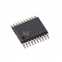
Low Profile 20-Terminal TSSOP Packaging
APPLICATIONS
D Digital Handset
D Digital Headset
D Cordless Phones
D Digital PABX
D Digital Voice Recording
DESCRIPTION
The TLV320AIC1106 PCM codec is designed to
perform transmit encoding analog-to-digital (A/D)
conversion, receive decoding digital-to-analog (D/A)
conversion, and transmit and receive filtering for
voice-band
communications
systems.
The
TLV320AIC1106 device operates in either the 13-bit
linear or 8-bit companded (µ-law) mode. The PCM
codec generates its own internal clocks from a
2.048-MHz master clock input.
PW PACKAGE
(TOP VIEW)
MICMUTE
RESET
VSS
EARVSS
EAROUT+
EARVDD
EAROUT−
EARVSS
MICGAIN+
MICIN−
1
2
3
4
5
6
7
8
9
10
20
19
18
17
16
15
14
13
12
11
EARMUTE
MCLK
PCMSYNC
PCMO
PCMI
DVSS
DVDD
LINSEL
MICGAIN −
MICIN+
This device contains circuits to protect its inputs and outputs against damage due to high static voltages or electrostatic fields. These
circuits have been qualified to protect this device against electrostatic discharges (ESD) of up to 2 kV according to MIL-STD-883C,
Method 3015; however, it is advised that precautions be taken to avoid application of any voltage higher than maximum-rated
voltages to these high-impedance circuits. During storage or handling, the device leads should be shorted together or the device
should be placed in conductive foam. In a circuit, unused inputs should always be connected to an appropriated logic voltage level,
preferably either VCC or ground. Specific guidelines for handling devices of this type are contained in the publication Guidelines for
Handling Electrostatic-Discharge-Sensitive (ESDS) Devices and Assemblies available from Texas Instruments.
Please be aware that an important notice concerning availability, standard warranty, and use in critical applications of
Texas Instruments semiconductor products and disclaimers thereto appears at the end of this data sheet.
����� ���� ���� ����������� �� ������� �� �� !�"#������� $���%
���$���� ������� �� �!������������ !�� �&� ����� �� ��'�� �����������
����$��$ (������)% ���$������ !��������* $��� ��� ���������#) ���#�$�
������* �� �## !���������%
Copyright 2001, Texas Instruments Incorporated
www.ti.com
1
���������
��
SLAS357 − DECEMBER 2001
functional block diagram
PCMI
PCMSYNC
(16)
(18)
(17)
PCMO
(19)
MCLK
MICGAIN −
PLL
TX
Filter
MIC Amp 1
(11)
+
(10)
−
MICIN −
MIC
Amp 2
LINSEL
EARVDD
EARVSS
VSS
DVSS
DVDD
Analog
Modulator
(1)
Digital
Modulator
and Filter
EARMUTE
(2)
(13)
(6)
(8) (4)
(3)
Power
and
Reset
(15)
(14)
RX = Receive
TX = Transmit
2
RX
Filter
(5)
EAR
AMP
(9)
MICMUTE
RESET
RX
Volume
Control
(12)
MICIN +
MICGAIN +
PCM
Interface
www.ti.com
(20)
EAROUT+
(7)
EAROUT−
���������
��
SLAS357 − DECEMBER 2001
detailed description
power up/reset
An external reset must be applied to the active-low RESET terminal while MCLK is active to ensure reset at
power up.
reference
A precision band-gap reference voltage is generated internally and supplies all required references to operate
the transmit and receive channels.
phase-locked loop
The phase-locked loop generates the internal clock frequency required for internal digital filters and modulators
by phase-locking to 2.048-MHz master clock input.
PCM interface
The PCM interface transmits and receives data at the PCMO and PCMI terminals, respectively. The data is
transmitted or received at the MCLK speed once on each PCMSYN cycle. The PCMSYN can be driven by an
external source that is derived from the master clock and used as an interrupt to the host controller.
microphone input
The microphone input circuit consists of two differential input/differential output amplifiers (MIC Amp 1 and
MIC Amp 2). MIC Amp 1 is a low-noise differential amplifier capable of an externally set gain. MIC Amp 2 is a
differential amplifier with a fixed gain of 6 dB.
analog modulator
The transmit channel modulator is a third-order sigma-delta design.
transmit filter
The transmit filter is a digital filter designed to meet Consultive Committee on International Telegraphy and
Telephony (CCITT) G.714 requirements. The TLV320AIC1106 device operates in either the 13-bit linear or 8-bit
companded µ-law mode.
receive filter
The receive (RX) filter is a digital filter that meets CCITT G.714 requirements. The TLV320AIC1106 device
operates in either the 13-bit linear or 8-bit µ-law companded mode, which is selected at the LINSEL input.
receive volume control
In linear mode, the three least significant bits of the 16-bit PCMI data sample is used to control volume. The
volume range is −18 dB to 3 dB in 3-dB steps.
digital modulator and filter
The second-order digital modulator and filter convert the received digital PCM data to the analog output required
by the earphone interface.
earphone amplifiers
EAROUT is recommended for use as a differential output; however, it can be connected in single-ended
topology as well. Clicks and pops are suppressed from the differential output.
www.ti.com
3
���������
��
SLAS357 − DECEMBER 2001
Terminal Functions
TERMINAL
TERMINAL
NO.
I/O
DESCRIPTION
EARVSS
4
I
Analog ground for EAROUT+
DVDD
14
I
Digital positive power supply
DVSS
15
I
Digital negative power supply
EARMUTE
20
I
Earphone mute
EAROUT−
7
O
Earphone amplifier negative output
EAROUT+
5
O
Earphone amplifier positive output
EARVDD
6
I
Analog positive power supply for the earphone amplifiers
EARVSS
8
I
Analog ground for EAROUT−
LINSEL
13
I
Companding enable
MCLK
19
I
Master system clock input (2.048 MHz) (digital)
MICGAIN+
9
I
Microphone gain positive feedback
MICGAIN−
12
I
Microphone gain negative feedback
MICMUTE
1
I
Microphone mute
MICIN−
10
I
Microphone negative input (−)
MICIN+
11
I
Microphone positive input (+)
PCMI
16
I
Receive PCM input
PCMO
17
O
Transmit PCM output
PCMSYNC
18
I
PCM frame synchronization
RESET
2
I
Active-low reset
VSS
3
I
Ground return for band-gap internal reference
absolute maximum ratings over operating free-air temperature range (unless otherwise noted)†
Supply voltage range, DVDD, EARVDD . . . . . . . . . . . . . . . . . . . . . . . . . . . . . . . . . . . . . . . . . . . . . . . . . . . −0.5 V to 3.6 V
Output voltage range, VO . . . . . . . . . . . . . . . . . . . . . . . . . . . . . . . . . . . . . . . . . . . . . . . . . . . . . . . . . . . . . . . −0.5 V to 3.6 V
Input voltage range, VI . . . . . . . . . . . . . . . . . . . . . . . . . . . . . . . . . . . . . . . . . . . . . . . . . . . . . . . . . . . . . . . . . . −0.5 V to 3.6 V
Continuous total power dissipation . . . . . . . . . . . . . . . . . . . . . . . . . . . . . . . . . . . . . . . . . . See Dissipation Rating Table
Operating free air temperature range, TA . . . . . . . . . . . . . . . . . . . . . . . . . . . . . . . . . . . . . . . . . . . . . . . . . . −40°C to 85°C
Storage temperature range, Tstg . . . . . . . . . . . . . . . . . . . . . . . . . . . . . . . . . . . . . . . . . . . . . . . . . . . . . . . . −65°C to 150°C
Lead temperature 1,6 mm from case for 10 seconds . . . . . . . . . . . . . . . . . . . . . . . . . . . . . . . . . . . . . . . . . . . . . . . 260°C
† Stresses beyond those listed under “absolute maximum ratings” may cause permanent damage to the device. These are stress ratings only, and
functional operation of the device at these or any other conditions beyond those indicated under “recommended operating conditions” is not
implied. Exposure to absolute-maximum-rated conditions for extended periods may affect device reliability.
DISSIPATION RATING TABLE
4
PACKAGE
TA ≤ 25°C
POWER RATING
DERATING FACTOR
ABOVE TA = 25°C
TA = 85°C
POWER RATING
PW
680 W
6.8 W/°C
270 W
www.ti.com
���������
��
SLAS357 − DECEMBER 2001
recommended operating conditions (see Note 2)
MIN
Supply voltage, DVDD, EARVDD
NOM
2.7
High-level input voltage, VIH
MAX
UNIT
3.3
V
0.7 x VDD
V
Low-level input voltage, VIL
0.3 x VDD
Load impedance between EAROUT+ and EAROUT−, RL
Ω
8 to 32
Input voltage, MICIN
V
0.9 x VDD
V
Operating free-air temperature, TA
−40
85
_C
NOTES: 1. To avoid possible damage and resulting reliability problems to these CMOS devices, follow the power-on initialization paragraph,
described in the Principles of Operations.
2. Voltages are with respect to DVSS, and EARVSS.
electrical characteristics over recommended ranges of supply voltage and operating free-air temperature
(unless otherwise noted)
supply current
PARAMETER
TEST CONDITIONS
MIN
Operating
IDD
Supply current from VDD
tpu
Power-up time from power down
Power down, MCLK not present
TYP
MAX
UNIT
5
7
mA
10
30
µA
10
ms
digital interface
PARAMETER
VOH
VOL
High-level output voltage, PCMO
IIH
IIL
High-level input current, any digital input
CI
Co
Low-level output voltage, PCMO
TEST CONDITIONS
IOH = − 3.2 mA,
IOL = 3.2 mA,
VDD = 3 V
VDD = 3 V
MIN
TYP
MAX
DVDD−0.25
UNIT
V
0.2
V
10
µA
10
µA
Input capacitance
10
pF
Output capacitance
20
pF
Low-level input current, any digital input
VI = 2.2 V to VDD
VI = 0 to 0.8 V
microphone interface
PARAMETER
VIO
IIB
Input offset voltage
Ci
Input capacitance
Vn
TEST CONDITIONS
See Note 3
Input bias current
MIN
TYP
MAX
5
mV
−250
250
nA
5
Microphone input referred noise, psophometric weighted
MIC Amp 1 gain = 23.5 dB,
See Note 4
MICMUTE
UNIT
−5
2.9
−80
pF
4
µVrms
dB
NOTES: 3. Measured while MICIN+ and MICIN− are connected together. Less than a 0.5-mV offset results in 0 value code on PCMOUT.
4. Configured as shown in Figure 3.
www.ti.com
5
���������
��
SLAS357 − DECEMBER 2001
electrical characteristics over recommended ranges of supply voltage and operating free-air temperature
(unless otherwise noted) (continued)
speaker interface
PARAMETER
TEST CONDITIONS
Earphone AMP output power (see Note 5)
IOmax
Maximum output current for EAROUT (rms)
MIN
TYP
MAX
VDD = 2.7 V, fully differential, 8-Ω load,
3-dBm0 output, volume control = − 3 dB,
PCMI data input to − 4 dB level
161
200
VDD = 2.7 V, fully differential, 16-Ω load,
3-dBm0 output, volume control = − 3 dB,
PCMI data input to − 2 dB level
128
160
VDD = 2.7 V, fully differential, 32-Ω load,
3-dBm0 output, volume control = − 3 dB,
PCMI data input to − 1 dB level
81
100
3-dBm0 input, 8-Ω load
141
178
3-dBm0 input, 16-Ω load
90
112
3-dBm0 input, 32-Ω load
50
63
EARMUTE
−80
UNIT
mW
mA
dB
NOTE 5: Maximum power is with a load impedance of −20%, at 25°C.
transmit gain and dynamic range, companded mode (µ-law) or linear mode selected (see Notes 6 and 7)
PARAMETER
TEST CONDITIONS
Transmit reference-signal level (0dB)
Differential, MIC Amp 1 configured for 23.5 dB gain
Overload-signal level (3 dBm0)
Differential, MIC Amp 1 configured for 23.5 dB gain
Absolute gain error
0 dBm0 input signal, 2.7 V ≤ VDD ≤ 3.3 V
MICIN−, MICIN+ to PCMO at 3 dBm0 to − 30 dBm0
Gain error with input level relative to gain at
−10 dBm0 MICIN, MICIN+ to PCMO
MIN
TYP
MAX
UNIT
88
mVpp
mVpp
124
−1
1
−0.5
0.5
MICIN−, MICIN+ to PCMO at − 31 dBm0 to − 45 dBm0
−1
1
MICIN−, MICIN+ to PCMO at − 46 dBm0 to − 55 dBm0
−1.2
1.2
dB
dB
NOTES: 6. Unless otherwise noted, the analog input is 0 dB, 1020-Hz sine wave, where 0 dB is defined as the zero-reference point of the channel
under test.
7. The reference signal level, which is input to the transmit channel, is defined as a value 3 dB below the full-scale value of 124-mVpp.
transmit filter transfer, companded mode (µ-law) or linear mode selected
PARAMETER
Gain relative to input signal gain at 1.02 kHz
6
TEST CONDITIONS
MIN
TYP
MAX
fMIC < 100 Hz
fMIC = 200 Hz
−0.5
0.5
−0.5
0.5
fMIC = 300 Hz to 3 kHz
fMIC = 3.4 kHz
−0.5
0.5
−1.5
0
fMIC = 4 kHz
fMIC = 4.6 kHz
−14
fMIC = 8 kHz
−47
www.ti.com
−35
UNIT
dB
���������
��
SLAS357 − DECEMBER 2001
electrical characteristics over recommended ranges of supply voltage and operating free-air temperature
(unless otherwise noted) (continued)
transmit idle channel noise and distortion, companded mode (µ-law) selected
PARAMETER
TEST CONDITIONS
MIN
MIC Amp 1 configured for 23.5-dB gain
(see Note 8)
Transmit idle channel noise, psophometrically weighted
Transmit signal-to-distortion ratio with 1.02-kHz sine-wave
input
Intermodulation distortion, 2-tone CCITT method, composite
power level, − 13 dBm0
TYP
−80
MICIN−, MICIN+ to PCMO at 3 dBm0
27
MICIN−, MICIN+ to PCMO at 0 dBm0
30
MICIN−, MICIN+ to PCMO at − 5 dBm0
33
MICIN−, MICIN+ to PCMO at − 10 dBm0
36
MICIN−, MICIN+ to PCMO at − 20 dBm0
35
MICIN−, MICIN+ to PCMO at − 30 dBm0
26
MICIN−, MICIN+ to PCMO at − 40 dBm0
24
MICIN−, MICIN+ to PCMO at − 45 dBm0
19
CCITT G.712 (7.1), R2
49
CCITT G.712 (7.2), R2
51
MAX
UNIT
−70
dBm0p
dBm0
dB
NOTE 8: With recommended impedances and resistor tolerance of 1%
transmit idle channel noise and distortion, linear mode selected
PARAMETER
Transmit idle channel noise, psophometrically weighted
Transmit signal-to-total distortion ratio with 1.02-kHz
sine-wave input
TEST CONDITIONS
MIN
MIC Amp 1 configured for 23.5-dB gain
(see Note 8)
TYP
MAX
UNIT
−80
−74
dBm0p
MICIN−, MICIN+ to PCMO at 3 dBm0
40
55
MICIN−, MICIN+ to PCMO at 0 dBm0
50
61
MICIN−, MICIN+ to PCMO at − 5 dBm0
52
62
MICIN−, MICIN+ to PCMO at −10 dBm0
56
66
MICIN−, MICIN+ to PCMO at −20 dBm0
52
68
MICIN−, MICIN+ to PCMO at − 30 dBm0
51
61
MICIN−, MICIN+ to PCMO at − 40 dBm0
43
59
MICIN−, MICIN+ to PCMO at − 45 dBm0
38
55
dB
NOTE 8: With recommended impedances and resistor tolerance of 1%
receive gain and dynamic range, linear or companded (µ-law) mode selected (see Note 9)
PARAMETER
Overload-signal level (3 dB)
Absolute gain error
TEST CONDITIONS
TYP
3.2
Load = 16 Ω, volume control = − 3 dB, PCMI data input to − 2 dB level
4.05
Load = 32 Ω, volume control = − 3 dB, PCMI data input to − 1 dB level
4.54
0 dBm0 input signal, 2.7 V ≤ VDD ≤ 3.3 V
PCMI to EAROUT−, EAROUT+ at 3 dBm0 to − 40 dBm0
Gain error with output level
relative to gain at −10 dBm0
MIN
Load = 8 Ω, volume control = − 3 dB, PCMI data input to − 4 dB level
MAX
UNIT
Vpp
−1
1
−0.5
0.5
PCMI to EAROUT−, EAROUT+ at − 41 dBm0 to − 50 dBm0
−1
1
PCMI to EAROUT−, EAROUT+ at − 51 dBm0 to − 55 dBm0
−1.2
1.2
dB
dB
NOTE 9: 1020-Hz input signal at PCMI, output measured differentially between EAROUT− and EAROUT+
www.ti.com
7
���������
��
SLAS357 − DECEMBER 2001
electrical characteristics over recommended ranges of supply voltage and operating free-air temperature
(unless otherwise noted) (continued)
receive filter transfer, companded mode (µ-law) or linear mode selected (MCLK = 2.048 MHz) (see Note 10)
PARAMETER
TEST CONDITIONS
MIN
TYP
fEAROUT < 100 Hz
fEAROUT = 200 Hz
Gain relative to input signal gain at 1.02-kHz
fEAROUT = 300 Hz to 3 kHz
fEAROUT = 3.4 kHz
MAX
UNIT
−15
−5
−0.5
0.5
−1.5
0
fEAROUT = 4 kHz
fEAROUT = 4.6 kHz
dB
−14
−35
fEAROUT = 8 kHz
NOTE 10: Volume control = − 3 dB, PCMI data input to − 1 dB level (32-Ω load)
−47
receive idle channel noise and distortion, companded mode (µ-law) selected (see Note 10)
PARAMETER
Receive noise, C-message weighted
Receive signal-to-distortion ratio with 1.02-kHz
sine-wave input
TEST CONDITIONS
MIN
PCMI = 11111111 (µ-law)
PCMI to EAROUT−, EAROUT+ at 3 dBm0
21
PCMI to EAROUT−, EAROUT+ at 0 dBm0
25
PCMI to EAROUT−, EAROUT+ at − 5 dBm0
36
PCMI to EAROUT−, EAROUT+ at −10 dBm0
43
PCMI to EAROUT−, EAROUT+ at − 20 dBm0
40
PCMI to EAROUT−, EAROUT+ at − 30 dBm0
38
PCMI to EAROUT−, EAROUT+ at − 40 dBm0
28
PCMI to EAROUT−, EAROUT+ at − 45 dBm0
23
TYP
MAX
UNIT
−90
−88
dBm0
dB
NOTE 10: Volume control = − 3 dB, PCMI data input to − 1 dB level (32-Ω load)
receive idle channel noise and distortion, linear mode selected (see Note 10)
PARAMETER
Receive noise, (20-Hz to 20-kHz brickwall window)
Receive signal-to-distortion ratio with 1.02-kHz
sine-wave input (0 −4 kHz)
Intermodulation distortion, 2-tone CCITT method,
composite power level, −13 dBm0
TEST CONDITIONS
TYP
MAX
UNIT
−83
−78
dBm0
PCMI to EAROUT−, EAROUT+ at 3 dBm0
48
52
PCMI to EAROUT−, EAROUT+ at 0 dBm0
51
56
PCMI to EAROUT−, EAROUT+ at − 5 dBm0
57
59
PCMI to EAROUT−, EAROUT+ at −10 dBm0
55
62
PCMI to EAROUT−, EAROUT+ at − 20 dBm0
51
53
PCMI to EAROUT−, EAROUT+ at − 30 dBm0
45
47
PCMI to EAROUT−, EAROUT+ at − 40 dBm0
42
47
PCMI to EAROUT−, EAROUT+ at − 45 dBm0
35
45
CCITT G.712 (7.1), R2
50
CCITT G.712 (7.2), R2
54
NOTE 10: Volume control = − 3 dB, PCMI data input to − 1 dB level (32-Ω load)
8
MIN
PCMI = 0000000000000
www.ti.com
dB
dB
���������
��
SLAS357 − DECEMBER 2001
electrical characteristics over recommended ranges of supply voltage and operating free-air temperature
(unless otherwise noted) (continued)
power supply rejection
PARAMETER
TEST CONDITIONS
MIN
TYP
MAX
UNIT
Supply voltage rejection, transmit channel
MICIN−, MICIN+ = 0 V, VDD = 2.7 V + 100 mVpp,
f = 1 kHz, Resistor tolerance of 1%
−74
−50
dB
Supply voltage rejection, receive channel
(differential)
PCM code = positive zero, VDD = 2.7 V + 100 mVpp,
f = 1 kHz, Resistor tolerance of 1%
−80
−65
dB
TYP
MAX
crosstalk attenuation, linear mode selected
PARAMETER
TEST CONDITIONS
MIN
UNIT
Crosstalk attenuation, transmit-to-receive
(differential)
MICIN−, MICIN+ = 0 dB, f = 300 Hz to 3400 Hz measured
differentially between EAROUT− and EAROUT+
70
dB
Crosstalk attenuation, receive-to-transmit
PCMI = 0 dBm0, f = 300 Hz to 3400 Hz measured at PCMO
70
dB
timing requirements
clock
MIN
tt
fmclk
NOM
MAX
Transition time, MCLK
10
MCLK frequency
2.048
UNIT
ns
MHz
MCLK jitter
37%
MCLK clock cycles per PCMSYN frame
256
256
cycles
transmit (see Figure 1)
MAX
UNIT
tsu(PCMSYN)
Setup time, PCMSYN high before MCLK ↓
MIN
20
tc(MCLK)−20
ns
th(PCMSYN)
Hold time, PCMSYN high after MCLK ↓
20
tc(MCLK)−20
receive (see Figure 2)
MIN
MAX
UNIT
tc(MCLK)−20
tc(MCLK)−20
ns
tsu(PCSYN)
th(PCSYN)
Setup time, PCMSYN high before MCLK ↓
20
Hold time, PCMSYN high after MCLK ↓
20
tsu(PCMI)
th(PCMI)
Setup time, PCMI high or low before MCLK ↓
20
ns
Hold time, PCMI high or low after MCLK ↓
20
ns
ns
switching characteristics over recommended operating conditions, CLmax = 10 pF (see Figure 1)
MIN
MAX
UNIT
tpd1
tpd2
Propagation delay time, MCLK bit 1 high to PCMO bit 1 valid
35
ns
Propagation delay time, MCLK high to PCMO valid, bits 2 to n
35
ns
tpd3
Propagation delay time, MCLK bit n low to PCMO bit n Hi-Z
www.ti.com
30
ns
9
���������
��
SLAS357 − DECEMBER 2001
PARAMETER MEASUREMENT INFORMATION
Transmit Time Slot
0
1
2
3
4
N−2
N−1
N
N+1
80%
MCLK
80%
20%
20%
tsu(PCMSYN)
ÎÎÎÎÎÎÎÎÎÎÎ
ÎÎÎÎÎÎÎÎÎÎÎ
th(PCMSYN)
PCMSYN
PCMO
1
2
tpd3
3
4
N−2
N−1
N
See Note C
tpd1
NOTES: A.
B.
C.
D.
See Note B
tpd2
See Note A
tsu(PCMO)
See Note D
This window is allowed for PCMSYN high.
This window is allowed for PCMSYN low (th(PCMSYN) max determined by data collision considerations).
Transitions are measured at 50%.
Bit 1 = Most significant bit (MSB), Bit N = Least significant bit (LSB)
Figure 1. Transmit Timing Diagram
Receive Time Slot
0
1
2
3
4
N −2
N −1
N
N +1
80%
80%
MCLK
ÎÎÎÎÎÎÎÎ
ÎÎÎÎ
ÎÎÎÎÎÎÎÎ
ÎÎÎÎ
tsu(PCMSYN)
PCMSYN
20%
20%
th(PCMSYN)
See Note A
PCMI
See Note C
1
See Note B
See Note D
2
th(PCMI)
3
4
N −2
N −1
tsu(PCMI)
NOTES: A.
B.
C.
D.
This window is allowed for PCMSYN high.
This window is allowed for PCMSYN low.
Transitions are measured at 50%.
Bit 1 = Most significant bit (MSB), Bit N = Least significant bit (LSB)
Figure 2. Receive Timing Diagram
10
www.ti.com
N
���������
��
SLAS357 − DECEMBER 2001
PRINCIPLES OF OPERATION
power-up initialization
An external reset with a minimum pulse width of 500 ns must be applied to the active-low RESET terminal with
MCLK active to ensure reset upon power up.
Table 1. Power-Up and Power-Down Power Consumption
(VDD = 2.7 V, Earphone Amplifier Loaded)
DEVICE STATUS
MAXIMUM POWER CONSUMPTION
Power up
16.2 mW
81 µW
Power down
The loss of MCLK (no transition detected) automatically enters the device into a power-down state with PCMO
in the high-impedance state. If an asynchronous power down occurs during a pulse code modulation (PCM)
data transmit cycle, the PCM interface remains powered up until the PCM data is completely transferred.
conversion laws
The device can be programmed either for a 13-bit linear or 8-bit (µ-law) companding mode. The companding
operation approximates the CCITT G.711 recommendation. The linear mode operation uses a 13-bit twos
complement format. Linear mode is selected with LINSEL low. LINSEL is high for companding.
transmit operation
microphone input
The microphone input stage is a low-noise differential amplifier. The microphone must be capacitively coupled
to the MICIN− and MICIN+ terminals. Preamplifier (MIC Amp 1) gain is determined by selection of external
resistors R2 and R3. To achieve the recommended gain setting of 23.5 dB for MIC Amp 1, resistor values of
R2 = 34 kΩ and R3 = 510 kΩ are suggested. A 1% tolerance is recommended for all resistors to meet the
specification. The recommended range for R2 is 34−100 kΩ. For values above 100 kΩ, the noise performance
of the channel is degraded.
+V
R3
R1
C1
R2
MICGAIN−
MICIN+
+
_
C1
R1 = 2 kΩ
C1 = 0.22 µF
MICIN−
R2
R1
MIC Amp 1
R3
MICGAIN+
ǒ Ǔ
MIC Amp 1 Gain in dB + 20 log R3
R2
Figure 3. Typical Microphone Interface
www.ti.com
11
���������
��
SLAS357 − DECEMBER 2001
PRINCIPLES OF OPERATION
microphone mute function
Transmit channel muting can be selected by setting MICMUTE high. Muting provides 80-dB attenuation of the
input microphone signal.
receive operation
earphone amplifier
The analog signal is routed to the earphone amplifier differential output (EAROUT− or EAROUT+), which is
capable of driving a load as low as 8 Ω. EAROUT is recommended for use as a differential output.
earphone mute function
Receive channel muting can be selected by setting the EARMUTE terminal to high.
receive PCM data format
D Companded mode: 8 bits are received, the MSB first
D Linear mode: 13 bits are received, the MSB first
Table 2. Receive Data Bit Definitions
12
BIT NO.
COMPANDED
MODE
LINEAR
MODE
1
CD7
LD12
2
CD6
LD11
3
CD5
LD10
4
CD4
LD9
5
CD3
LD8
6
CD2
LD7
7
CD1
LD6
8
CD0
LD5
9
−
LD4
10
−
LD3
11
−
LD2
12
−
LD1
13
−
LD0
14
−
RXVOL2
15
−
RXVOL1
16
−
RXVOL0
www.ti.com
���������
��
SLAS357 − DECEMBER 2001
PRINCIPLES OF OPERATION
receive volume control
In linear mode, RXVOL [2:0] PCM data bits are used for volume control according to Table 3. Volume control
bits must be sent on PCMI for each 13-bit receive word. In companded mode, volume control is fixed at 0 dB.
Table 3. Volume Control Bit Definition in Linear Mode
RXVOL [2:0]
GAIN SETTING
000
3 dB
001
0 dB
010
−3 dB
011
−6 dB
100
−9 dB
101
−12 dB
110
−15 dB
111
−18 dB
support section
The clock generator and control circuit uses the master clock input (MCLK) to generate internal clocks to drive
internal counters, filters, and converters.
clock frequencies and sample rates
A fixed PCMSYN rate of 8 kHz determines the sampling rate. The PCMSYN signal must be derived from the
master clock. The divide ratio must be set to 256 for the device to work properly.
www.ti.com
13
���������
��
SLAS357 − DECEMBER 2001
TYPICAL CHARACTERISTICS
RELATIVE GAIN
vs
FREQUENCY
20
10
0
0
−20
−10
Relative Gain − dB
Relative Gain − dB
RELATIVE GAIN
vs
FREQUENCY
−40
See Note A
−60
−20
See Note B
−30
−80
−40
−100
−50
−120
−60
0
1
2
3
4
5
6
0
1
f − Frequency − kHz
2
3
4
5
6
f − Frequency − kHz
Figure 4
Figure 5
NOTES: A. Transmit channel frequency response shown relative to the gain at a 1.02-kHz input signal in linear mode.
B. Receive channel frequency response shown relative to the gain at a 1.02-kHz input signal in linear mode.
RELATIVE GAIN
vs
FREQUENCY
20
10
0
0
−20
−10
Relative Gain − dB
Relative Gain − dB
RELATIVE GAIN
vs
FREQUENCY
−40
See Note A
−60
−20
See Note B
−30
−80
−40
−100
−50
−120
−60
0
1
2
3
4
5
6
f − Frequency − kHz
0
1
2
3
4
f − Frequency − kHz
Figure 6
Figure 7
NOTES: A. Transmit channel frequency response shown relative to the gain at a 1.02-kHz input signal in µ-Law mode.
B. Receive channel frequency response shown relative to the gain at a 1.02-kHz input signal in µ-Law mode.
14
www.ti.com
5
6
���������
��
SLAS357 − DECEMBER 2001
TYPICAL CHARACTERISTICS
SUPPLY CURRENT
vs
SUPPLY VOLTAGE
SUPPLY CURRENT
vs
SUPPLY VOLTAGE
10
20
16
See Note A
Supply Current − µ A
Supply Current − mA
8
6
4
See Note B
12
2
0
2.5
8
4
3
3.5
Supply Voltage − V
0
2.5
3
3.5
Supply Voltage − V
Figure 8
Figure 9
NOTES: A. Supply current as a function of supply voltage in power-up mode.
B. Supply current as a function of supply voltage in power-down mode.
www.ti.com
15
�PACKAGE OPTION ADDENDUM
www.ti.com
14-Oct-2022
PACKAGING INFORMATION
Orderable Device
Status
(1)
Package Type Package Pins Package
Drawing
Qty
Eco Plan
(2)
Lead finish/
Ball material
MSL Peak Temp
Op Temp (°C)
Device Marking
(3)
Samples
(4/5)
(6)
TLV320AIC1106PW
ACTIVE
TSSOP
PW
20
70
RoHS & Green
NIPDAU
Level-1-260C-UNLIM
-40 to 85
AIC1106
Samples
TLV320AIC1106PWG4
ACTIVE
TSSOP
PW
20
70
RoHS & Green
NIPDAU
Level-1-260C-UNLIM
-40 to 85
AIC1106
Samples
TLV320AIC1106PWR
ACTIVE
TSSOP
PW
20
2000
RoHS & Green
NIPDAU
Level-1-260C-UNLIM
-40 to 85
AIC1106
Samples
(1)
The marketing status values are defined as follows:
ACTIVE: Product device recommended for new designs.
LIFEBUY: TI has announced that the device will be discontinued, and a lifetime-buy period is in effect.
NRND: Not recommended for new designs. Device is in production to support existing customers, but TI does not recommend using this part in a new design.
PREVIEW: Device has been announced but is not in production. Samples may or may not be available.
OBSOLETE: TI has discontinued the production of the device.
(2)
RoHS: TI defines "RoHS" to mean semiconductor products that are compliant with the current EU RoHS requirements for all 10 RoHS substances, including the requirement that RoHS substance
do not exceed 0.1% by weight in homogeneous materials. Where designed to be soldered at high temperatures, "RoHS" products are suitable for use in specified lead-free processes. TI may
reference these types of products as "Pb-Free".
RoHS Exempt: TI defines "RoHS Exempt" to mean products that contain lead but are compliant with EU RoHS pursuant to a specific EU RoHS exemption.
Green: TI defines "Green" to mean the content of Chlorine (Cl) and Bromine (Br) based flame retardants meet JS709B low halogen requirements of


 工商网监
湘ICP备2023018690号
工商网监
湘ICP备2023018690号