TLV320AIC12, TLV320AIC13
TLV320AIC14, TLV320AIC15
TLV320AIC12K, TLV320AIC14K
www.ti.com
SLWS115E – OCTOBER 2001 – REVISED JANUARY 2007
LOW-POWER, HIGHLY-INTEGRATED, PROGRAMMABLE
16-Bit, 26-KSPS MONO CODEC
FEATURES
•
•
•
•
•
•
•
•
•
•
Mono 16-Bit Oversampling Sigma-Delta A/D
Converter
Mono 16-Bit Oversampling Sigma-Delta D/A
Converter
Support Maximum Master Clock of 100 MHz to
Allow the DSP Output Clock to be Used as a
Master Clock
Selectable FIR/IIR Filter With Bypassing
Option
Programmable Sampling Rate up to:
– Max 26 Ksps With On-Chip IIR/FIR Filter
– Max 104 Ksps With IIR/FIR Bypassed
On-Chip FIR Produced 84-dB SNR for ADC
and 92-dB SNR for DAC
Smart Time Division Multiplexed
(SMARTDM™) Serial Port
– Glueless 4-Wire Interface to DSP
– Automatic Cascade Detection (ACD)
Self-Generates Master/Slave Device
Addresses
– Programming Mode to Allow On-the-Fly
Reconfiguration
– Continuous Data Transfer Mode to
Minimize Bit Clock Speed
– Support Different Sampling Rate for Each
Device
– Turbo Mode to Maximize Bit Clock for
Faster Data Transfer and Allow Multiple
Serial Devices to Share the Same Bus
– Allows up to 16 Devices to be Connected
to a Single Serial Port
Host Port
– 2-Wire Interface
– Selectable I2C or S2C
Differential and Single-Ended Analog
Input/Output
Built-In Analog Functions:
•
•
•
•
•
•
– Analog and Digital Sidetone
– Antialiasing Filter (AAF)
– Programmable Input and Output Gain
Control (PGA)
– Microphone/Handset/Headset Amplifiers
– AIC12K has an 8-Ω Speaker Driver
– Power Management With
Hardware/Software Power-Down Modes
30 µW
Separate Software Control for ADC and DAC
Power Down
Fully Compatible With Common TMS320™
DSP Family and Microcontroller Power
Supplies
– 1.65 V - 1.95 V Digital Core Power
– 1.1 V - 3.6 V Digital I/O
– 2.7 V - 3.6 V Analog
Power Dissipation (PD)
– 11.2 mW at 3.3 V in Standard Operation
– 17.8 mW at 3.3 V With Headphone Drivers
Internal Reference Voltage (Vref)
2s Complement Data Format
Test Modes Which Include Digital Loopback
and Analog Loopback
APPLICATIONS
•
•
•
•
•
Digital Still Cameras
Wireless Accessories
Hands-Free Car Kits
VOIP
Cable Modem
Please be aware that an important notice concerning availability, standard warranty, and use in critical applications of Texas
Instruments semiconductor products and disclaimers thereto appears at the end of this data sheet.
SMARTDM, TMS320C5000, TMS320C6000 are trademarks of Texas Instruments.
TMS320 is a trademark of Texas Instrument.
PRODUCTION DATA information is current as of publication date.
Products conform to specifications per the terms of the Texas
Instruments standard warranty. Production processing does not
necessarily include testing of all parameters.
Copyright © 2001–2007, Texas Instruments Incorporated
�TLV320AIC12, TLV320AIC13
TLV320AIC14, TLV320AIC15
TLV320AIC12K, TLV320AIC14K
www.ti.com
SLWS115E – OCTOBER 2001 – REVISED JANUARY 2007
These devices have limited built-in ESD protection. The leads should be shorted together or the device placed in conductive foam
during storage or handling to prevent electrostatic damage to the MOS gates.
DESCRIPTION
The TLV320AIC1x is a true low-cost, low-power, high-integrated, high-performance, mono voice codec. It
features one 16-bit analog-to-digital (A/D) channel and one 16-bit digital-to-analog (D/A) channel.
The TLV320AIC1x provides high-resolution signal conversion from digital-to-analog (D/A) and from
analog-to-digital (A/D) using oversampling sigma-delta technology with programmable sampling rate.
The TLV320AIC1x implements the smart time division multiplexed serial port (SMARTDM™). The SMARTDM
port is a synchronous 4-wire serial port in TDM format for glue-free interface to TI DSPs (i.e. TMS320C5000™,
TMS320C6000™) and microcontrollers. The SMARTDM supports both continuous data transfer mode and
on-the-fly reconfiguration programming mode. The TLV320AIC1x can be gluelessly cascaded to any
SMARTDM-based device to form multichannel codec and up to 16 TLV320AIC1x codecs can be cascaded to a
single serial port.
The TLV320AIC1x also provides a flexible host port. The host port interface is a two-wire serial interface that
can be programmed to be either an industrial standard I2C or a simple S2C (start-stop communication protocol).
The TLV320AIC1x also integrates all of the critical functions needed for most voice-band applications including
MIC preamplifier, handset amplifier, headset amplifier, antialiasing filter (AAF), input/output programmable gain
amplifier (PGA), and selectable low-pass IIR/FIR filters. The AIC12K also includes an 8-Ω speaker driver.
The TLV320AIC1x implements an extensive power management; including device power-down, independent
software control for turning off ADC, DAC, operational-amplifiers, and IIR/FIR filter (bypass) to maximize system
power conservation. The TLV320AIC1x consumes only 11.2 mW at 3.3 V.
The TLV320AIC1x low power operation from 2.7 V to 3.6 V power supplies, along with extensive power
management, make it ideal for portable applications including wireless accessories, hands free car kits, VOIP,
cable modem, and speech processing. Its low group delay characteristic makes it suitable for single or
multichannel active control applications.
The TLV320AIC1x is characterized for commercial operation from 0°C to 70°C and industrial operation from
-40°C to 85°C. The TLV320AIC1xk is characterized for industrial operation from -40°C to 85°C.
ORDERING INFORMATION
PRODUCT
2
(1)
PACKAGE
DESIGNATOR
OPERATING
TEMPERATURE
RANGE, TA
TLV320AIC1xC
TSSOP-30
DBT
0°C to 70°C
TLV320AIC1xI
TSSOP-30
DBT
-40°C to 85°C
TLV320AIC12K
QFN-32
RHB
-40°C to 85°C
TLV320AIC14K
(1)
PACKAGE
QFN-32
RHB
-40°C to 85°C
ORDERING
NUMBER
TRANSPORT MEDIA,
QUANTITY
TLV320AIC1xCDBT
Tape and Reel, 250
TLV320AIC1xCDBTR
Tape and Reel, 3000
TLV320AIC1xIDBT
Tape and Reel, 250
TLV320AIC1xIDBTR
Tape and Reel, 3000
TLV320AIC12KIRHBT
Tape and Reel, 250
TLV320AIC12KIRHBR
Tape and Reel, 3000
TLV320AIC14KIRHBT
Tape and Reel, 250
TLV320AIC14KIRHBR
Tape and Reel, 3000
For the most current package and ordering information, see the Package Option Addendum at the end of this document, or see the TI
Web site at www.ti.com.
Submit Documentation Feedback
�TLV320AIC12, TLV320AIC13
TLV320AIC14, TLV320AIC15
TLV320AIC12K, TLV320AIC14K
www.ti.com
SLWS115E – OCTOBER 2001 – REVISED JANUARY 2007
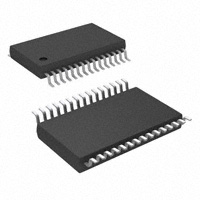
AIC12/13/12K DBT PACKAGE
(TOP VIEW)
DVSS
DVDD
SCLK
SDA
SCL
MCLK
RESET
INP1
INM1
BIAS
INM2
INP2
MICIN
AVDD
AVSS
30
29
28
27
26
25
24
23
22
21
20
19
18
17
16
IOVSS
IOVDD
FSD
FS
DOUT
DIN
M/S
PWRDN
OUTM1
OUTP1
DRVDD
DRVSS
NC
NC
NC
1
2
3
4
5
6
7
8
9
10
11
12
13
14
15
INM2
16
N/C
INM2
23
22
21
20
DRVSS
24
25
N/C
17
N/C
18
N/C
19
AVSS
20
INP2
21
DRVSS
OUTP3
22
OUTMV
AVSS
23
AIC14K RHB PACKAGE
(TOP VIEW)
OUTP2
AVDD
24
25
MICIN
INP2
AIC12K RHB PACKAGE
(TOP VIEW)
DVSS
DVDD
SCLK
SDA
SCL
MCLK
RESET
INP1
INM1
BIAS
INM2
INP2
MICIN
AVDD
AVSS
30
29
28
27
26
25
24
23
22
21
20
19
18
17
16
AVDD
1
2
3
4
5
6
7
8
9
10
11
12
13
14
15
MICIN
IOVSS
IOVDD
FSD
FS
DOUT
DIN
M/S
PWRDN
OUTM1
OUTP1
DRVDD
DRVSS
OUTP2
OUTMV
OUTP3
AIC14/15/14K DBT PACKAGE
(TOP VIEW)
19
18
17
16
N/C
N/C
26
15
DRVDD
N/C
26
15
DRVDD
BIAS
27
14
OUTP1
BIAS
27
14
OUTP1
28
13
OUTM1
INM1
28
13
OUTM1
INM1
INP1
29
12
PWRDN
INP1
29
12
PWRDN
11
M/S
10
DIN
DIN
MCLK
31
SCL
31
SCL
31
2
3
4
5
6
7
8
SDA
SCLK
DVDD
DVSS
IOVSS
IOVDD
FSD
FS
9
1
DOUT
9
1
2
3
4
5
6
7
8
FS
10
FSD
31
IOVDD
MCLK
IOVSS
RESET
DVSS
M/S
DVDD
11
SCLK
30
SDA
RESET
30
DOUT
NOTE: For the RHB package, connect the device thermal pad to DRVDD.
Submit Documentation Feedback
3
�TLV320AIC12, TLV320AIC13
TLV320AIC14, TLV320AIC15
TLV320AIC12K, TLV320AIC14K
www.ti.com
SLWS115E – OCTOBER 2001 – REVISED JANUARY 2007
Terminal Functions
TERMINAL
NAME
4
AIC12/13/12K
DBT
NO.
AIC14/15/14K
DBT
NO.
AIC12K
RHB
NO.
AIC14K
RHB
NO.
I/O
IOVSS
1
1
5
5
I
Digital I/O ground
IOVDD
2
2
6
6
I
Digital I/O power supply
DESCRIPTION
FSD
3
3
7
7
O
Frame sync delayed output. The FSD output synchronizes a slave
device to the frame sync of the master device. FSD is applied to the
slave FS input and is the same duration as the master FS signal. This
pin must be pulled low if AIC1x is a stand-alone slave. It must be
pulled high if the AIC1x is a stand-alone master or the last slave in the
cascade.
FS
4
4
8
8
I/O
Frame sync. When FS goes low, DIN begins receiving data bits and
DOUT begins transmitting data bits. In master mode, FS is internally
generated. In slave mode, FS is externally generated.
DOUT
5
5
9
9
O
Data output. DOUT transmits the ADC output bits and registers data,
and is synchronized to SCLK and FS. Data is sent out at the rising
edge of SCLK. Outside data/control frame, DOUT is put in 3-state.
DIN
6
6
10
10
I
Data input. DIN receives the DAC input data and register data from the
external DSP (digital signal processor) and is synchronized to SCLK
and FS. Data is latched at the falling edge of SCLK.
M/S
7
7
11
11
I
Master/slave select input. When M/S is high, the device is the master,
and when low it is a slave.
PWRDN
8
8
12
12
I
Power down. When PWRDN is pulled low, the device goes into a
power-down mode, the serial interface is disabled, and most of the
high-speed clocks are disabled. However, all the register values are
sustained and the device resumes full-power operation without
reinitialization when PWRDN is pulled high again. PWRDN resets the
counters only and preserves the programmed register contents.
OUTM1
9
9
13
13
O
Inverting output of the DAC. OUTM1 is functionally identical with and
complementary to OUTP1. This differential output can drive a
maximum load of 600 Ω. This output can also be used alone for
single-ended operation.
OUTP1
10
10
14
14
O
Noninverting output of the DAC. This differential output can drive a
maximum load of 600 Ω. This output can also be used alone for
single-ended operation.
DRVDD
11
11
15
15
I
Analog power supply for the 16-Ω drivers OUTP2 and OUTP3
DRVSS
12
12
17
17
I
Analog ground for the 16-Ω drivers OUTP2 and OUTP3
OUTP2
13
–
18
–
O
Analog output number 2 from the 16-Ω driver. This output can drive a
maximum load of 16 Ω, and also can be configured as either
single-ended output or differential output by the control register 6.
OUTMV
14
–
19
–
O
Programmable virtual ground for the output of OUTP2 and OUTP3
(see the Register Map).
OUTP3
15
–
20
–
O
Analog output number 3 from the 16-Ω driver. This output can drive a
maximum load of 16 Ω, and also be configured as either single-ended
output or differential output by the control register 6.
AVSS
16
16
21
21
I
Analog ground
AVDD
17
17
22
22
I
Analog power supply
MICIN
18
18
23
23
I
MIC preamplifier input. It must be connected to AVSS if not used.
INP2
19
19
24
24
I
Noninverting analog input 2. It must be connected to AVSS if not used.
INM2
20
20
25
25
I
Inverting analog input 2. It must be connected to AVSS if not used.
BIAS
21
21
27
27
O
Bias output voltage is software selectable between 1.35 V and 2.35 V.
Its output current is 5 mA.
INM1
22
22
28
28
I
Inverting analog input 1. It must be connected to AVSS if not used.
INP1
23
23
29
29
I
Noninverting analog input 1. It must be connected to AVSS if not used.
RESET
24
24
30
30
I
Hardware reset. The reset function is provided to initialize all of the
internal registers to their default values. The serial port is configured to
the default state accordingly.
MCLK
25
25
31
31
I
Master clock. MCLK derives the internal clocks of the sigma-delta
analog interface circuit.
SCL
26
26
32
32
I
Programmable host port (I2C or S2C) clock input.
SDA
27
27
1
1
I/O
Programmable host port (I2C or S2C) data line.
Submit Documentation Feedback
�TLV320AIC12, TLV320AIC13
TLV320AIC14, TLV320AIC15
TLV320AIC12K, TLV320AIC14K
www.ti.com
SLWS115E – OCTOBER 2001 – REVISED JANUARY 2007
Terminal Functions (continued)
TERMINAL
NAME
AIC12/13/12K
DBT
NO.
AIC14/15/14K
DBT
NO.
AIC12K
RHB
NO.
AIC14K
RHB
NO.
I/O
DESCRIPTION
Shift clock. SCLK signal clocks serial data into DIN and out of DOUT
during the frame-sync interval. When configured as an output (M/S
high), SCLK is generated internally by multiplying the frame-sync signal
frequency by 16 and the number of codecs in cascade in standard and
continuous mode. When configured as an input (M/S low), SCLK is
generated externally and must be synchronous with the master clock
and frame sync.
SCLK
28
28
2
2
I/O
DVDD
29
29
3
3
I
Digital power supply
DVSS
30
30
4
4
I
Digital ground
16, 26
16, 18, 19, 20,
26
NC
–
13, 14, 15
No connection
Electrical Characteristics
AIC12, AIC13, AIC14, AIC15, AIC12K, AIC14K: Over Recommended Operating Free-Air Temperature Range
AVDD = 3.3 V, DVDD = 1.8 V, IOVDD = 3.3 V (Unless Otherwise Noted)
Absolute Maximum Ratings
Over Operating Free-Air Temperature Range (Unless Otherwise Noted) (1)
UNITS
VCC
Supply voltage range:
DVDD (2)
-0.3 V to 2.25 V
AVDD, DRVDD, IOVDD
(2)
-0.3 V to 4 V
VO
Output voltage range, all digital output signals
-0.3 V to IOVDD + 0.3 V
VI
Input voltage range, all digital input signals
-0.3 V to IOVDD + 0.3 V
TA
Operating free-air temperature range
TJ
Junction temperature
Tstg
Storage temperature range
-40°C to 85°C
105°C
-65°C to 150°C
(TJmax - TA ) / θJA
Power dissipation
θJA
Thermal impedance
44°C/W
Case temperature for 10 seconds: Package
ESD Characteristics
(1)
(2)
260°C
AIC12, AIC13, AIC14, AIC15, AIC12k and AIC14k all
pins
CDM
500 V
AIC12, AIC13, AIC14, AIC15, AIC12k and AIC14k all
pins except for the following:
HBM
2 kV
DVDD, SDA
HBM
1.3 kV
DOUT
HBM
1.9 kV
Stresses beyond those listed under absolute maximum ratings may cause permanent damage to the device. These are stress ratings
only and functional operation of the device at these or any other conditions beyond those indicated under recommended operating
conditions is not implied. Exposure to absolute-maximum-rated conditions for extended periods may affect device reliability.
All voltage values are with respect to VSS.
Submit Documentation Feedback
5
�TLV320AIC12, TLV320AIC13
TLV320AIC14, TLV320AIC15
TLV320AIC12K, TLV320AIC14K
www.ti.com
SLWS115E – OCTOBER 2001 – REVISED JANUARY 2007
Recommended Operating Conditions
MIN
NOM
MAX
MIN
AIC12/13/14/15
VSS
VI(analog)
Supply voltage for analog, AVDD
2.7
Supply voltage for analog output driver, DRVDD
2.7
CL
3.6
2.7
3.6
2.7
3.3
3.6
V
3.6
1.65
1.8
1.95
1.65
1.8
1.95
V
1.1
3.3
3.6
1.1
3.3
3.6
V
2
V
Analog single-ended peak-to-peak input voltage
2
Output load resistance,
600
600
Between OUTP2 and
OUTMV (single-ended)
16
16
Between OUTP3 and
OUTMV (single-ended)
16
16
Between OUTP2 and
OUTMV (differential)
32
32
Between OUTP3 and
OUTMV (differential)
32
32
Ω
Analog output load capacitance
20
20
Digital output capacitance
20
20
pF
100
100
MHz
26
kHz
85
°C
ADC or DAC conversion rate
6
UNIT
Supply voltage for digital I/O, IOVDD
Master clock
TA
MAX
Supply voltage for digital core, DVDD
Between OUTP1 and
OUTM1 (differential)
RL
3.3
NOM
AIC12K/14K
Operating free-air temperature
26
-40
Submit Documentation Feedback
85
-40
pF
�TLV320AIC12, TLV320AIC13
TLV320AIC14, TLV320AIC15
TLV320AIC12K, TLV320AIC14K
www.ti.com
SLWS115E – OCTOBER 2001 – REVISED JANUARY 2007
Digital Inputs and Outputs
Fs = 8 kHz, Outputs Not Loaded
PARAMETER (1)
MIN
TYP
MAX
High-level output voltage, DOUT
VOL
Low-level output voltage, DOUT
IIH
High-level input current, any digital input
0.5
µA
IIL
Low-level input current, any digital input
0.5
µA
CI
Input capacitance
3
pF
Co
Output capacitance
5
pF
(1)
0.8 IOVDD
UNIT
VOH
V
0.1 IOVDD
V
For VIH (Input high level), when IOVDD < 1.6 V, minimum VIH is 1.1V.
ADC Path Filter
Fs = 8 KHz
(1) (2)
PARAMETER
TEST
CONDITIONS
MIN
TYP
MAX
MIN
FIR FILTER
Filter gain relative to gain
at 1020 Hz
(1)
(2)
TYP
MAX
UNIT
IIR FILTER
0 Hz to 30 Hz
-0.5
0.2
-0.5
0.2
300 Hz to 3 Hz
-0.5
0.25
-0.5
0.25
3.3 Hz
-0.5
0.3
-1.5
0.3
3.6 KHz
-3
-3
4 kHz
-35
-20
≥ 4.4 KHz
-74
-60
dB
The filter gain outside of the passband is measured with respect to the gain at 1020 Hz. The analog input test signal is a sine wave with
0 dB = 4 VI(PP) as the reference level for the analog input signal. The pass band is 0 to 3600 Hz for an 8-KHz sample rate. This pass
band scales linearly with the sample rate.
The filter characteristics are specified by design and are not tested in production.
Submit Documentation Feedback
7
�TLV320AIC12, TLV320AIC13
TLV320AIC14, TLV320AIC15
TLV320AIC12K, TLV320AIC14K
www.ti.com
SLWS115E – OCTOBER 2001 – REVISED JANUARY 2007
ADC DYNAMIC PERFORMANCE
Fs = 8 KHz
(1)
PARAMETER
TEST
CONDITIONS
MIN
TYP
MAX
MIN
AIC12/13/14/15
SNR
Signal-to-noise ratio
VI = -1 dB
82
88
VI = -9 dB
78
82
VI = -40 dB
THD
Total harmonic distortion
THD+N
VI = -1 dB
84
90
VI = -9 dB
82
88
UNIT
AIC12K/14K
75
88
82
75
90
88
dB
67
VI = -1 dB
79
87
87
VI = -9 dB
73
79
79
VI = -40 dB
(1)
MAX
46
VI = -40 dB
Signal-to-harmonic
distortion + noise
TYP
48
The test condition is a differential 1020-Hz input signal with an 8-KHz conversion rate. Input and output common mode is 1.35 V.
ADC CHANNEL CHARACTERISTICS
PARAMETER
TEST
CONDITIONS
MIN
TYP
MAX
AIC12/13/14/15
Preamplifier gain = 6
dB
VI(pp)
Single-ended input level
VIO
Input offset voltage
MICIN, INPx, INMx
IB
Input bias current
MICIN, INPx, INMx
Common-mode voltage
Dynamic range
Mute attenuation
Gain error
EO(ADC)
ADC converter offset error
CMRR
Common-mode rejection
ratio at INMx and INPx
Idle channel noise
MAX
UNIT
AIC12K/14K
2
±10
2
±10
34
V
mV
34
µA
1.35
V
VI = -1 dB
85
85
dB
PGA = MUTE
80
80
dB
87
87
dB
VI = -1 dB at 1020 Hz
0.6
0.6
dB
±10
±10
mV
VI = -1 dB at 1020 Hz
50
50
dB
V(INP,INM,MICIN) = 0 V
50
50
µVrms
100
RI
Input resistance
TA = 25°C
30
30
kΩ
CI
Input capacitance
TA = 25°C
2
2
pF
IIR
5/fs
5/fs
S
FIR
17/fs
17/fs
S
Channel delay
8
TYP
1.35
Intrachannel isolation
EG
MIN
Submit Documentation Feedback
�TLV320AIC12, TLV320AIC13
TLV320AIC14, TLV320AIC15
TLV320AIC12K, TLV320AIC14K
www.ti.com
SLWS115E – OCTOBER 2001 – REVISED JANUARY 2007
DAC Path Filter
Fs = 8 KHz
(1) (2)
TEST
CONDITIONS
PARAMETER
MIN
TYP
MAX
MIN
FIR FILTER
(2)
MAX
UNIT
IIR FILTER
0 Hz to 30 Hz
-0.5
0.2
-0.5
0.2
300 Hz to 3 Hz
-0.25
0.25
-0.25
0.35
3.3 Hz
-0.35
0.3
-0.75
0.3
Filter gain relative to gain
at 1020 Hz
(1)
TYP
3.6 KHz
-3
-3
4 kHz
-40
-20
≥ 4.4 KHz
-74
-60
dB
The filter gain outside of the passband is measured with respect to the gain at 1020 Hz. The input signal is the digital equivalent of a
sine wave (digital full scale = 0 dB). The nominal differential DAC channel output with this input condition = 4 VI(PP). The pass band is 0
to 3600 Hz for an 8-KHz sample rate. This pass band scales linearly with the sample rate.
The filter characteristics are specified by design and are not tested in production.
DAC DYNAMIC PERFORMANCE
TEST
CONDITIONS
PARAMETER
MIN
TYP
MAX
MIN
AIC12/13/14/15
TYP
MAX
UNIT
AIC12k/14k
DAC Line Output (OUTP1, OUTM1) (1)
SNR
Signal-to-noise ratio
VI = 0 dB
80
92
VI = -9 dB
75
83
VI = -40 dB
THD
Total harmonic
distortion
Signal-to-total harmonic
distortion + noise
VI = 0 dB
78
85
VI = -9 dB
74
83
SNR
Signal-to-noise ratio
THD
Total harmonic
distortion
THD+N
Signal-to-total harmonic
distortion + noise
DAC Speaker Output (OUTP2, OUTMV)
(1)
(2)
(3)
83
70
85
83
dB
62
VI = 0 dB
75
82
82
VI = -9 dB
70
77
77
VI = -40 dB
DAC Headphone Output (OUTP2, OUTP3)
92
51
VI = -40 dB
THD+N
75
44
(1) (2)
VI = 0 dB
78
89
89
VI = -9 dB
71
81
81
VI = 0 dB
78
82
82
VI = -9 dB
73
80
80
VI = 0 dB
75
80
80
VI = -9 dB
69
78
78
dB
dB
dB
(1) (3)
SNR
Signal-to-noise ratio
VI = 0 dB
91
dB
THD
Total harmonic
distortion
VI = 0 dB
80
dB
The test condition is the digital equivalent of a 1020 Hz input signal with an 8-kHz conversion rate. The test is measured at output of
application schematic low-pass filter. The test is conducted in 16-bit mode.
The DAC headphone output spec between OUTP2, OUTP3, and OUTMV is valid only for the AIC12/13 and the AIC12K
The DAC speaker output spec between OUTP2, OUTP3, and OUTMV is valid only for the AIC12K.
Submit Documentation Feedback
9
�TLV320AIC12, TLV320AIC13
TLV320AIC14, TLV320AIC15
TLV320AIC12K, TLV320AIC14K
www.ti.com
SLWS115E – OCTOBER 2001 – REVISED JANUARY 2007
DAC Channel Characteristics
PARAMETER
TEST CONDITIONS
Dynamic range
MIN
VI = 0 dB at 1020 Hz
Interchannel isolation
EG
Gain error, 0 dB
VO = 0 dB at 1020 Hz
Common mode voltage
TYP
92
dB
dB
0.5
dB
1.35
0 kHz-4 kHz
(1)
80
VOO
Output offset voltage at OUT (differential)
DIN = All zeros
10
VO
Analog output voltage, (3.3 V)
OUTP
IIR
FIR
(1)
(2)
(3)
(4)
Maximum output power
V
125 (2)
µVrms
mV
0.35
600 Ω load at 3.3 V between
OUTP1 and OUTM1
UNIT
120
Idle channel narrow band noise
P(O)
MAX
2.35
V
6.7
16 Ω load at 3.3 V between
single-ended OUTP2/OUTMV and
OUTP3/OUTMV (3)
62.5
16 Ω load at 3.3 V between
differential OUTP2/OUTP3 and
OUTMV (4)
125
8 Ω load at 3.3 V between
differential OUTP2/OUTP3 and
OUTMV (4)
190
mW
5/fs
Channel delay
s
18/fs
The conversion rate is 8 kHz.
The Max value is valid only for the AIC12/13/14/15.
The specification for maximum power output for single ended load between OUTP2/OUTMV and OUTP3/OUTMV is valid only for the
AIC12/13 and AIC12K.
The specification for maximum power output for differential load between OUTP2/OUTP3 and OUTMV is valid only for the AIC12/13 and
AIC12K.
BIAS Amplifier Characteristics
PARAMETER
TEST CONDITIONS
MIN
TYP
MAX
MIN
AIC12/13/14/15
VO
Output voltage
UNIT
2.35
V
20
µV
Offset voltage
10
10
mV
Current drive
10
10
mA
1
1
MHz
140
120
300 Hz-13 kHz
Unity gain bandwidth
DC gain
2.35
MAX
20
Integrated noise
2.2
TYP
AIC12K/14K
2.4
dB
OUTMV Amplifier Characteristics
PARAMETER
TEST CONDITIONS
MIN
TYP
MAX
AIC12/13/14/15
VO
Output voltage
Integrated noise
Offset voltage
Current drive
Unity gain bandwidth
DC gain
10
1.3
300 Hz-13 kHz
1.35
MIN
TYP
MAX
UNIT
AIC12K/14K
1.4
1.35
V
20
20
µV
10
10
mV
62.5
62.5
mA
1
1
MHz
120
120
Submit Documentation Feedback
dB
�TLV320AIC12, TLV320AIC13
TLV320AIC14, TLV320AIC15
TLV320AIC12K, TLV320AIC14K
www.ti.com
SLWS115E – OCTOBER 2001 – REVISED JANUARY 2007
Power-Supply Rejection
(1)
PARAMETER
TEST CONDITIONS
AVDD
Supply-voltage rejection ratio, analog supply (fj = 0 to fs/2) at 1 kHz
DVDD
Supply-voltage rejection ratio, DAC channel
(1)
DAC channel
ADC channel
MIN
TYP
Differential
75
Single-ended
50
MAX
dB
95
fj = 0 kHz to 30 kHz
UNIT
dB
86
Power supply rejection measurements are made with both the ADC and DAC channels idle and a 200 mV peak-to-peak signal applied
to the appropriate supply.
Power Supply
PARAMETER
TEST CONDITIONS
MIN
TYP
MAX
AIC12/13/14/15
PD
Power dissipation (1)
I(total)
Total current (1)
17.8
23.1
17.8
Without 16-Ω drivers
11.2
16.5
11.2
All sections on
5.4
7
5.4
Without 16-Ω drivers
3.4
5
3.4
0.01
0.01
2
2
ADC
Supply current
analog
digital (2)
IDD
(1)
(2)
Supply current, PLL
TYP
DAC
1
1
0.4
0.4
16-Ω drivers
2
2
Coarse sampling
1
1
1.4
1.4
1
1
Ref
IDD Analog
IDD Digital
MAX
UNIT
AIC12K/14K
All sections on
Power down
IDD
MIN
mW
mA
mA
mA
mA
Excludes digital
All section ON except the PLL condition.
Submit Documentation Feedback
11
�TLV320AIC12, TLV320AIC13
TLV320AIC14, TLV320AIC15
TLV320AIC12K, TLV320AIC14K
www.ti.com
SLWS115E – OCTOBER 2001 – REVISED JANUARY 2007
Functional Block Diagram AIC12/13/12k
s2d
MICIN
Preamplifier
24, 12, 6, 0 dB
INP2
INM2
Decimation Filter
AntiAliasing
Filter
MUX
INP1
PGA
SigmaDelta
ADC
Sinc
Filter
SMARTDM
Serial
Port
FIR Filter
IIR Filter
- 42 dB to 20 dB
Step Size = 1 dB
INM1
DOUT
DIN
Digital Loopback
w/ Sidetone Control
and Mute
-3 dB to -21 dB
Analog
Loopback
OUTP1
(600 Ω Driver)
OUTM1
OUTP2
FS
SCLK
FSD
Interpolation Filter
PGA
Low Pass
Filter
SigmaDelta
DAC
Sinc
Filter
FIR Filter
IIR Filter
- 42 dB to 20 dB
Step Size = 1 dB
d2s
(16 ΩDriver)
OUTP3
M/S
Vref
d2s
Host Port
(16 ΩDriver)
SCL
SDA
OUTMV
Internal Clock Circuit
BIAS
1.35 V/2.35 V @ 5 mA max
12
Submit Documentation Feedback
Div
16xMxNxP
MCLK
�TLV320AIC12, TLV320AIC13
TLV320AIC14, TLV320AIC15
TLV320AIC12K, TLV320AIC14K
www.ti.com
SLWS115E – OCTOBER 2001 – REVISED JANUARY 2007
Functional Block Diagram AIC14/15/14k
MICIN
s2d
Preamplifier
24, 12, 6, 0 dB
INP2
INM2
Decimation Filter
AntiAliasing
Filter
MUX
INP1
PGA
SigmaDelta
ADC
Sinc
Filter
SMARTDM
Serial
Port
FIR Filter
IIR Filter
− 42 dB to 20 dB
Step Size = 1 dB
INM1
DOUT
DIN
Digital Loopback
w/ Sidetone Control
and Mute
−3 dB to −21 dB
Analog
Loopback
OUTP1
(600 Ω Driver)
OUTM1
M/S
FS
SCLK
FSD
Interpolation Filter
PGA
Low-Pass
Filter
SigmaDelta
DAC
Sinc
Filter
FIR Filter
IIR Filter
− 42 dB to 20 dB
Step Size = 1 dB
Vref
Host Port
BIAS
SCL
SDA
1.35 V/2.35 V @ 5 mA max
Internal Clock Circuit
Submit Documentation Feedback
Div
16xMxNxP
MCLK
13
�TLV320AIC12, TLV320AIC13
TLV320AIC14, TLV320AIC15
TLV320AIC12K, TLV320AIC14K
www.ti.com
SLWS115E – OCTOBER 2001 – REVISED JANUARY 2007
Definitions and Terminology
Term
Definition
Data Transfer
Interval
The time during which data is transferred from DOUT and to DIN. The interval
is 16 shift clocks and the data transfer is initiated by the falling edge of the FS
signal in standard and continuous mode.
Signal Data
This refers to the input signal and all of the converted representations through
the ADC channel and the signal through the DAC channel to the analog output.
This is contrasted with the purely digital software control data.
Frame Sync
Frame sync refers only to the falling edge of the signal FS that initiates the data
transfer interval
Frame Sync and Sampling
Period
Frame sync and sampling period is the time between falling edges of
successive FS signals.
fs
The sampling frequency
ADC Channel
ADC channel refers to all signal processing circuits between the analog input
and the digital conversion result at DOUT.
DAC channel
DAC channel refers to all signal processing circuits between the digital data
word applied to DIN and the differential output analog signal available at OUTP
and OUTM.
Dxx
Bit position in the primary data word (xx is the bit number)
DSxx
Bit position in the secondary data word (xx is the bit number)
PGA
Programmable gain amplifier
IIR
Infinite impulse response
FIR
Finite impulse response
14
Submit Documentation Feedback
�TLV320AIC12, TLV320AIC13
TLV320AIC14, TLV320AIC15
TLV320AIC12K, TLV320AIC14K
www.ti.com
SLWS115E – OCTOBER 2001 – REVISED JANUARY 2007
Timing Requirements
twH
2.4 V
MCLK
2.4 V
twL
tsu1
th1
2.4 V
RESET
Figure 1. Hardware Reset Timing
SCLK
td1
td2
td2
td1
FS
FSD
td3
ten
DOUT
tdis
D15
tsu2
th2
DIN
D15
Figure 2. Serial Communication Timing
TEST CONDITIONS
MIN
TYP
MAX
twH
Pulse duration, MCLK high
5
twL
Pulse duration, MCLK low
5
tsu1
Setup time, RESET, before MCLK high
(see Figure 1)
3
th1
Hold time, RESET, after MCLK high (see Figure 1)
td1
Delay time, SCLK↑ to FS/FSD↓
td2
Delay time, SCLK↑ to FS/FSD↑
td3
Delay time, SCLK↑ to DOUT
15
ten
Enable time, SCLK↑ to DOUT
15
tdis
Disable time, SCLK↑ to DOUT
tsu2
Setup time, DIN, before SCLK↓
10
th2
Hold time, DIN, after SCLK↓
10
UNIT
2
CL = 20 pF
5
ns
5
15
Submit Documentation Feedback
15
�TLV320AIC12, TLV320AIC13
TLV320AIC14, TLV320AIC15
TLV320AIC12K, TLV320AIC14K
www.ti.com
SLWS115E – OCTOBER 2001 – REVISED JANUARY 2007
SDA
tf
tLOW
tSU;OAT
tr
tf
tHD;STA
tBUF
tr
SCL
tHD;STA
tHD;DAT
tSU;STA
tHIGH
tSU;STO
Figure 3. I2C / S2C Timing
TEST CONDITIONS
MIN
MAX
UNIT
0
900
kHz
tSCL
SCL clock frequency
tHD;STA
Hold time (repeated START condition. After this
period, the first clock pulse is generated.
100
ns
tLOW
Low period of the SCL clock
560
ns
tHIGH
High period of the SCL clock
560
ns
tSU;STA
Set-up time for a repeated START condition
100
ns
tHD;DAT
Data hold time
50
ns
tSU;DAT
Data set-up time
50
tr
Rise time of both SDA and SCL signals
300
ns
tf
Fall time of both SDA and SCL signals
100
ns
tSU;STO
Set-up time for STOP condition
100
ns
tBUF
Bus free time between a STOP and START condition
500
ns
CL = 20 pF
ns
Parameter Measurement Information
Amplitude - dB
0
-20
Sampling Rate at 8 kHz
-40
-60
-80
-100
-120
-140
-160
0
500
1000
1500
2000
2500
f - Frequency - Hz
3000
Figure 4. FFT—ADC Channel (-1 dB Input)
16
Submit Documentation Feedback
3500
4000
�TLV320AIC12, TLV320AIC13
TLV320AIC14, TLV320AIC15
TLV320AIC12K, TLV320AIC14K
www.ti.com
SLWS115E – OCTOBER 2001 – REVISED JANUARY 2007
Parameter Measurement Information (continued)
Amplitude - dB
0
-20
Sampling Rate at 8 kHz
-40
-60
-80
-100
-120
-140
-160
0
500
1000
1500
2000
2500
f - Frequency - Hz
3000
3500
4000
Figure 5. FFT—ADC Channel (-9 dB Input)
Amplitude - dB
0
-20
Sampling Rate at 8 kHz
-40
-60
-80
-100
-120
-140
-160
0
500
1000
1500
2000
2500
f - Frequency - Hz
3000
3500
4000
Figure 6. FFT—DAC Channel (0 dB Input)
Amplitude - dB
0
-20
Sampling Rate at 8 kHz
-40
-60
-80
-100
-120
-140
-160
0
500
1000
1500
2000
2500
f - Frequency - Hz
3000
3500
4000
Figure 7. FFT—DAC Channel (-9 dB Input)
Submit Documentation Feedback
17
�TLV320AIC12, TLV320AIC13
TLV320AIC14, TLV320AIC15
TLV320AIC12K, TLV320AIC14K
www.ti.com
SLWS115E – OCTOBER 2001 – REVISED JANUARY 2007
Parameter Measurement Information (continued)
0
ADC at 8 kHz
Fs = 32 kHz
Amplitude - dB
-20
-40
-60
-80
-100
-120
-140
0
2000
4000
6000
8000
10000
f - Frequency - Hz
12000
14000
16000
Figure 8. FFT—ADC Channel in FIR/IIR Bypass Mode (-1 dB Input)
0
DAC at 8 kHz
Fs = 32 kHz
Amplitude - dB
-20
-40
-60
-80
-100
-120
-140
0
2000
4000
6000
8000
10000
f - Frequency - Hz
12000
14000
Figure 9. FFT—DAC Channel in FIR/IIR Bypass Mode (0 dB Input)
18
Submit Documentation Feedback
16000
�TLV320AIC12, TLV320AIC13
TLV320AIC14, TLV320AIC15
TLV320AIC12K, TLV320AIC14K
www.ti.com
SLWS115E – OCTOBER 2001 – REVISED JANUARY 2007
TYPICAL CHARACTERISTICS
ADC FILTER GAIN
vs
FREQUENCY RESPONSE (FIR)
ADC FILTER GAIN
vs
FREQUENCY RESPONSE (IIR)
5
5
0
0
−5
−10
Filter Gain − dB
Filter Gain − dB
−5
−10
−15
−15
−20
−25
−30
−20
−35
−25
−40
−30
−45
0
500
1000 1500 2000 2500 3000 3500 4000
0
500
1000 1500 2000 2500 3000 3500 4000
f − Frequency − Hz
Figure 10.
Figure 11.
ADC IIR FILTER GROUP DELAY
vs
FREQUENCY
DAC IIR FILTER GROUP DELAY
vs
FREQUENCY RESPONSE
9
9
8
8
7
7
Group Delay - fs
Group Delay - fs
f − Frequency − Hz
6
5
4
6
5
4
3
3
2
2
1
1
0
0
0
500
1000 1500 2000 2500 3000 3500 4000
0
500
f - Frequency - Hz
1000 1500 2000 2500 3000 3500 4000
f - Frequency - Hz
Figure 12.
Figure 13.
Submit Documentation Feedback
19
�TLV320AIC12, TLV320AIC13
TLV320AIC14, TLV320AIC15
TLV320AIC12K, TLV320AIC14K
www.ti.com
SLWS115E – OCTOBER 2001 – REVISED JANUARY 2007
TYPICAL CHARACTERISTICS (continued)
DAC FILTER GAIN
vs
FREQUENCY (FIR/IIR BYPASS)
4
4
2
2
0
0
-2
-2
Filter Gain - dB
Filter Gain - dB
ADC FILTER GAIN
vs
FREQUENCY (FIR/IIR BYPASS)
-4
-6
-8
-4
-6
-8
-10
-10
-12
-12
-14
-14
0
2000 4000 6000 8000 10 k
12 k 14 k
16 k
0
2000 4000 6000 8000 10 k
f - Frequency - Hz
Figure 14.
Figure 15.
DAC IIR
vs
FREQUENCY RESPONSE
DAC FIR
vs
FREQUENCY RESPONSE
OSR = 512
OSR = 128
0
0
−20
Filter Gain − dB
Filter Gain − dB
−20
−40
−60
−80
−40
−60
−80
−100
−100
−120
1000 2000 3000 4000 5000 6000 7000 8000
f − Frequency − Hz
−140
0
Figure 16.
20
16 k
20
20
−120
0
12 k 14 k
f - Frequency - Hz
1000 2000 3000 4000 5000 6000 7000 8000
f − Frequency − Hz
Figure 17.
Submit Documentation Feedback
�TLV320AIC12, TLV320AIC13
TLV320AIC14, TLV320AIC15
TLV320AIC12K, TLV320AIC14K
www.ti.com
SLWS115E – OCTOBER 2001 – REVISED JANUARY 2007
TYPICAL CHARACTERISTICS (continued)
DAC FIR
vs
FREQUENCY RESPONSE
DAC FIR
vs
FREQUENCY RESPONSE
20
20
OSR = 128
0
0
−20
−20
−40
−40
Filter Gain − dB
Filter Gain − dB
OSR = 256
−60
−80
−60
−80
−100
−100
−120
−120
−140
0
1000 2000 3000 4000 5000 6000 7000 8000
−140
0
1000 2000 3000 4000 5000 6000 7000 8000
f − Frequency − Hz
f − Frequency − Hz
Figure 18.
Figure 19.
Functional Description
Operating Frequencies (see Notes)
The sampling frequency is the frequency of the frame sync (FS) signal whose falling edge starts digital-data
transfer for both ADC and DAC. The sampling frequency is derived from the master clock (MCLK) input by the
following equations:
• Coarse sampling frequency (default):
– The coarse sampling is selected by programming P = 8 in the control register 4, which is the default
configuration of AIC1x on power-up or reset.
– FS = Sampling (conversion) frequency = MCLK ÷ (16 × M × N × 8)
• Fine sampling frequency (see step 5):
– FS = Sampling (conversion) frequency = MCLK ÷ (16 × M × N × P)
NOTES:
1. Use control register 4 to set the following values of M, N, and P
2. M = 1, 2, . . . , 128
3. N = 1, 2,..., 16
4. P = 1, 2, ..., 8
5. The fine sampling rate needs an on-chip Phase Lock Loop (frequency multiplier) to generate
internal clocks. The PLL requires the relationship between MCLK and P to meet the following
condition:
10 MHz ≤ (MCLK ÷ P) ≤ 25 MHz. The output of the PLL is only used to generate internal clocks
that are needed by the data converters. Other clocks such as the serial interface clocks in master
mode are not generated from the PLL output. The clock generation scheme is as shown in
Figure 20.
Submit Documentation Feedback
21
�TLV320AIC12, TLV320AIC13
TLV320AIC14, TLV320AIC15
TLV320AIC12K, TLV320AIC14K
www.ti.com
SLWS115E – OCTOBER 2001 – REVISED JANUARY 2007
Functional Description (continued)
X8
(DLL)
Digital
MCLK
1/(MN)
1/P
128 FS
en_dll
SCLK *
(no_dev x mode) / (MNP)
1 / (16 x mode x no_dev)
FS
* SCLK may not be an uniform clock depending upon values of devnum, mode, and MNP
M = 1 - 128
When P = 8, DLL(PLL) is enabled
N = 1 - 16
devnum = number of devices in cascade
P = 1- 8
mode = 1 (for continious data tranfer mode)
mode = 2 (for programming mode)
Figure 20. AIC1x Clock Tree Architecture
6. Both equation of FS require that the following conditions be met:
– (M × N × P) ≥ (devnum × mode) if the FIR/IIR filter is not bypassed.
– [Integer (M ÷ 4) × N × P] ≥ (devnum × mode) if the FIR/IIR filter is bypassed.
Where:
– devnum is the number of codec channels connecting in cascade mode.
– mode is equal to 1 for continuous data transfer mode and 2 for programming mode.
7. If the DAC OSR is set to 512, then M needs to be a multiple of 4. If the DAC OSR is set to 256,
then M needs to be a multiple of 2. M can take any value between 1 and 128 if the OSR is set to
128.
EXAMPLE:
The MCLK that comes from the DSP 'C5402 CLKOUT equals to 20.48 MHz, and the conversion rate
of 8 kHz is desired. First, set P = 1 to satisfy condition step 5 above so that (MCLK ÷ P) = 20.48 MHz
÷ 1 = 20.48 MHz. Next, pick M = 10 and N = 16 to satisfy step 6 above and derive 8 kHz for FS.
20.48 MHz
FS +
+ 8 kHz
(16 10 16 1)
Internal Architecture
Analog Low-Pass Filter
The built-in analog low-pass filter is a two-pole filter that has a 20-dB attenuation at 1 MHz.
Sigma-Delta ADC
The analog-to-digital converter is a sigma-delta modulator with 128-x oversampling. The ADC provides
high-resolution, low-noise performance using oversampling techniques. Due to the oversampling employed, only
single pole R-C filters are required on the analog inputs.
22
Submit Documentation Feedback
�TLV320AIC12, TLV320AIC13
TLV320AIC14, TLV320AIC15
TLV320AIC12K, TLV320AIC14K
www.ti.com
SLWS115E – OCTOBER 2001 – REVISED JANUARY 2007
Functional Description (continued)
Decimation Filter
The decimation filters are either FIR filters or IIR filters selected by bit D5 of the control register 1. The FIR filter
provides linear-phase output with 17/fs group delay, whereas the IIR filter generates nonlinear phase output with
negligible group delay. The decimation filters reduce the digital data rate to the sampling rate. This is
accomplished by decimating with a ratio of 1:128. The output of the decimation filter is a 16-bit 2s-complement
data word clocking at the sample rate selected. The BW of the filter is (0.45 × FS) and scales linearly with the
sample rate.
Sigma-Delta DAC
The digital-to-analog converter is a sigma-delta modulator with 128/256/512-x oversampling. The DAC provides
high-resolution, low-noise performance using oversampling techniques. The oversampling ratio in DAC is
programmable to 256/512 using bits D4-D3 of control register 3, the default being 128. Oversampling ratio of
512 can be used when FS is a maximum of 8 Ksps and an oversampling ratio of 256 can be used when FS is a
maximum of a 16 Ksps. M should be a multiple of 2 for an oversampling ratio of 256 and 4 for oversampling
ratio of 512.
Interpolation Filter
The interpolation filters are either FIR filters or IIR filters selected by bit D5 of the control register 1. The FIR filter
provides linear-phase output with 18/fs group delay, whereas the IIR filter generates nonlinear phase output with
negligible group delay. The interpolation filter resamples the digital data at a rate of 128/256/512 times the
incoming sample rate, based on the oversampling rate of DAC. The high-speed data output from the
interpolation filter is then used in the sigma-delta DAC. The BW of the filter is (0.45 × FS) and scales linearly
with the sample rate.
Analog/Digital Loopback
The analog and digital loopbacks provide a means of testing the data ADC/DAC channels and can be used for
in-circuit system level tests. The analog loopback always has the priority to route the DAC low pass filter output
into the analog input where it is then converted by the ADC to a digital word. The digital loopback routes the
ADC output to the DAC input on the device. Analog loopback is enabled by writing a 1 to bit D2 in the control
register 1. Digital loopback is enabled by writing a 1 to bit D1 in control register 1.
Side-Tone Loopback
The side-tone digital loopback attenuates the ADC output and mixes it with the input of the DAC. The level of the
side tone is set by DSTG, bits D5-D3 of the control register 5C.
ADC PGA
TLV320AIC1x has a built-in PGA for controlling the signal levels at ADC outputs. ADC PGA gain setting can be
selected by writing into bits D5-D0 of register 5A. The PGA range of the ADC channel is 20 dB to -42 dB in
steps of 1 dB and mute. To avoid sudden jumps in signal levels with PGA changes, the gains are applied
internally with zero-crossovers.
DAC PGA
TLV320AIC1x has a built-in PGA for controlling the analog output signal levels in DAC channel. DAC PGA gain
setting can selected by writing into bits D5-D0 of register 5B. The PGA range of the DAC channel is 20 dB to -42
dB in steps of 1 dB, and mute. To avoid sudden pop-sounds with power-up/down and gain changes the
power-up/down and gain changes for DAC channel are applied internally with zero-crossovers.
Analog Input/Output
The TLV320AIC1x has three programmable analog inputs and three programmable analog outputs. Bits D2-D1
of control register 6 select the analog input source from MICIN, INP1/M1, or INP2/M2. All analog I/O are either
single-ended or differential. All analog input signals are self-biased to 1.35 V. The three analog outputs are
configured by bits D7, D6, D5, and D4-D3 of control register 6.
Submit Documentation Feedback
23
�TLV320AIC12, TLV320AIC13
TLV320AIC14, TLV320AIC15
TLV320AIC12K, TLV320AIC14K
www.ti.com
SLWS115E – OCTOBER 2001 – REVISED JANUARY 2007
Functional Description (continued)
MIC Input
TLV320AIC1x supports single ended microphone input. This can be used by connecting the external single
ended source through ac coupling to the MICIN pin. This channel is selected by writing 01 or 10 into bits D2-D1
in control register 6. The single ended input is supported in two modes.
Writing 01 into bits D2-D1 chooses self biased MICIN mode. In this mode, the device internally self-biases the
input at 1.35V. For best noise performance, the user should bias the microphone circuit using the BIAS voltage
generated by the device as shown in Figure 21.
Writing 10 into bits D2-D1 chooses pseudo-differential MICIN mode. In this mode, the single ended input is
connected through ac-coupling to MICIN and the bias voltage used to generate the signal is also ac coupled to
INM1 as shown in Figure 22. For best noise performance, the MICIN and INM1 lines must be routed in similar
fashion from the microphone to the device for noise cancellation.
For high quality performance, the single ended signal is converted internally into differential signal before being
converted. To improve the dynamic range with different types of microphones, the device supports a preamplifier
with gain settings of 0/6/12/24 dB. This can be chosen by writing into bits D1-D0 of control register 5C.
Electret
Microphone
0.1 µF
10 kΩ
BIAS
INM1
0.1 µF
Electret
Microphone
MICIN
10 kΩ
0.1 µF
BIAS
MICIN
TLV320AIC12
TLV320AIC12
(a) Single Ended
(b) Pseudo -Differential (High Quality)
Figure 21. Microphone Interface
INP and INM Input
To produce common-mode rejection of unwanted signal performance, the analog signal is processed
differentially until it is converted to digital data. The signal applied to the terminals INM1/2 and INP1/2 are
differential to preserve device specifications (see Figure 22). The signal source driving analog inputs (INP1/2
and INM1/2) should have low source impedance for lowest noise performance and accuracy. To obtain
maximum dynamic range, the signal should be ac-coupled to the input terminal.
INP1 or INP2
V(INP)
1.35 V
INM1 or INM2
V(INM)
TLV320AIC12
Figure 22. INP and INM Internal Self-Biased Circuit
Single-Ended Analog Input
The two differential inputs of (INP1/M1 and INP2/M2) can be configured to work as single-ended inputs by
connecting INP to the analog input and INM to ground (see Figure 23).
24
Submit Documentation Feedback
�TLV320AIC12, TLV320AIC13
TLV320AIC14, TLV320AIC15
TLV320AIC12K, TLV320AIC14K
www.ti.com
SLWS115E – OCTOBER 2001 – REVISED JANUARY 2007
Functional Description (continued)
C
INP1 or INP2
Analog Input
C
INM1 or INM2
Figure 23. Single-Ended Input
Analog Output
The OUTP and OUTM are differential output from the DAC channel. The OUTP1 and OUTM1 can drive a load
of 600-Ω directly and be either differential or single-ended (see Figure 24). The OUTP2 and OUTP3 are output
from two audio amplifiers to drive low-voltage speakers like those in the handset and headset. They can drive a
load of 16-Ω directly and be configured as either differential output or single-ended output as by bit D7 of the
control register 6 (see Figure 25). If OUTP2 and OUTP3 are differential output, the OUTMV pin becomes the
common inverting output. Both OUTP2 and OUTP3 can be used simultaneously if each differential load RL >
32Ω . This is because OUTMV amplifier can drive a maximum load of 16 Ω only (only one driver used) or a
parallel combination of two 32-Ω loads (both drivers used). If both OUTP2 and OUTP3 are used simultaneously,
they are muted at the same time if MUTE is selected.
Otherwise, the OUTMV pin is configured as the virtual ground for single-ended output and equal to the common
mode voltage at 1.35 V.
C
OUTP1
OUTP1
RL
RL
OUTM1
OUTM1
Differential Output OUTP/OUTM
Single-Ended Output OUTP/OUTM
Figure 24. OUTP1/OUTM1 Output
OUTP2
RL
OUTMV
RL
OUTP3
Figure 25. Single-Ended/Differential Connection of OUTP2/OUTP3 Output
Analog Output Configuration
SPEAKER DRIVER CONFIGURATION
NO. OF SPEAKER DRIVERS ON
MIN LOAD
Single-ended
1
16-Ω
Single-ended
2
32-Ω
Differential
1
16-Ω
Submit Documentation Feedback
25
�TLV320AIC12, TLV320AIC13
TLV320AIC14, TLV320AIC15
TLV320AIC12K, TLV320AIC14K
www.ti.com
SLWS115E – OCTOBER 2001 – REVISED JANUARY 2007
Functional Description (continued)
Analog Output Configuration (continued)
SPEAKER DRIVER CONFIGURATION
NO. OF SPEAKER DRIVERS ON
MIN LOAD
Differential
2
32-Ω
IIR/FIR Control
Overflow Flags
The decimation IIR/FIR filter sets an overflow flag (bit D7) of control register 1 indicating that the input analog
signal has exceeded the range of internal decimation filter calculations. The interpolation IIR/FIR filter sets an
overflow flag (bit D4) of control register 1 indicating that the digital input has exceeded the range of internal
interpolation filter calculations. When the IIR/FIR overflow flag is set in the register, it remains set until the user
reads the register. Reading this value resets the overflow flag. These flags need to be reset after power-up by
reading the register. If FIR/IIR overflow occurs, the input signal is attenuated by either the PGA or some other
method.
IIR/FIR Bypass Mode
An option is provided to bypass IIR/FIR filter sections of the decimation filter and the interpolation filter. This
mode is selected through bit D6 of control register 2 and effectively increases the frequency of the FS signal to
four times normal output rate of the IIR/FIR-filter. For example, for a normal sampling rate of 8 Ksps (i.e., FS =
8 kHz) with IIR/FIR, if the IIR/FIR is bypassed, the frequency of FS is readjusted to 4×8 kHz = 32 kHz. The sinc
filters of the two paths can not be bypassed. A maximum of eight devices in cascade can be supported in the
IIR/FIR bypassed mode.
In this mode , the ADC channel outputs data which has been decimated only until 4Fs. Similarly DAC channel
input needs to be preinterpolated to 4Fs before being given to the device. This mode allows users the flexibility
to implement their own filter in DSP for decimation and interpolation. M should be a multiple of 4 during IIR/FIR
Bypass mode. The frequency responses of the IIR/FIR bypass modes are shown in Figure 14 and Figure 15.
System Reset and Power Management
Software and Hardware Reset
The TLV320AIC1x resets internal counters and registers in response to either of two events:
• A low-going reset pulse is applied to terminal RESET
• A 1 is written to the programmable software reset bits (D5 of control register 3)
•
NOTE: The TLV320AIC1x requires a power-up reset applied to the RESET pin before normal operation is
started.
Either event resets the control registers and clears all sequential circuits in the device. The H/W RESET (active
low) signal is at least 6 master clock periods long. As soon as the RESET input is applied, the TLV320AIC1x
enters the initialization cycle that lasts for 132 MCLKs, during which the serial port of the DSP must be tristated.
The initialization sequence performed by the 'AIC1x is known as auto cascade detection (ACD). ACD is a
mechanism that allows a device to know its address in a cascade chain. Up to 16 'AIC1x devices can be
cascaded together. The master device is the first device on the chain (i.e. the FS of the master is connected to
the FS of the DSP). During ACD, each device gets to know the number of devices in the chain as well as its
relative position in the chain. This is done on hardware reset. Therefore, after power up, a hardware reset must
be done. ACD requires 132 MCLKs after reset to complete operation. The number of MCLKs is independent of
the number of devices in the chain. Adjacent devices in the chain have their FS and FSD pins connected to
each other. The master device FS is connected to the FS pin of the DSP. The FSD pin on the last device in the
chain is pulled high. The master device has the highest address (i.e. 0, the next device in the chain has an
address of 1, followed by 2 etc.).
During the first 64 MCLKs, FS is configured as an output and FSD as an input. During the next 64 MCLKs, FS is
configured as an input and FSD as an output. The master device always has FS configured as an output and
the last slave in the cascade (i.e. channel with address 0) always has FSD configured as an input.
26
Submit Documentation Feedback
�TLV320AIC12, TLV320AIC13
TLV320AIC14, TLV320AIC15
TLV320AIC12K, TLV320AIC14K
www.ti.com
SLWS115E – OCTOBER 2001 – REVISED JANUARY 2007
To calculate the channel address, during the first 64 MCLKs, the device counts the number of clocks between
ACD starting (reset) and the FSD going high. During the next 64 MCLKs, the device counts the number of
clocks till FS is pulled low. The sum total of the counts in the first phase and the second phase is the number of
devices in the channel.
For a cascaded system, the rise time of H/W RESET needs to be less than the MCLK period and should satisfy
setup time requirement of 2 ns with respect to MCLK rise-edge. In stand-alone-slave mode SCLK must be
running during RESET. If more than one codec is cascaded, RESET must be synchronized to MCLK.
Additionally, all devices must see the same edge of MCLK within a window of 0.5 ns The reset signal need not
be synchronized with MCLK when the codec is in stand-alone master or slave configuration.
Power Management
Most of the device (all except the digital interface) enters the power-down mode when D7 and D6, in control
register 3, are set to 1. When the PWRDN pin is low, the entire device is powered down. In either case, register
contents are preserved.
The amount of power drawn during software power down is higher than during a hardware power down because
of the current required to keep the digital interface active. Additional differences between software and hardware
power-down modes are detailed in the following paragraphs.
Software Power-Down
Data bits D7 and D6 of control register 3 are used by TLV320AIC1x to turn on or off the software power-down
mode, which takes effect in the next frame FS. The ADC and DAC can be powered down individually. In the
software power-down, the digital interface circuit is still active while the internal ADC and DAC channel and
differential outputs OUTPx and OUTMx are disabled, and DOUT is put in 3-state in the data frame only. Register
data in the control frame is still accepted via DIN, but data in the data frame is ignored. The device returns to
normal operation when D7 and D6 of control register 3 are reset.
Hardware Power-Down
The TLV320AIC1x requires the PWRDN signal to be synchronized with MCLK. When PWRDN is held low, the
device enters hardware power-down mode. In this state, the internal clock control circuit and the differential
outputs are disabled. All other digital I/Os are disabled and DIN cannot accept any data input. The device can
only be returned to normal operation by holding PWRDN high. Getting out of the power-down mode (i.e. bringing
PWRDN from low to high state) requires that the low-to-high transition of PWRDN be synchronous to the rising
edge of MCLK. If there is no need for the hardware power-down mode feature of the device, the PWRDN pin
must be tied high.
Host Port Interface
The host port uses a 2-wire serial interface (SCL, SDA) to program the AIC1x's six control registers and
selectable protocol between S2C mode and I2C mode. The S2C is a write-only mode and the I2C is a read-write
mode selected by setting the bits D1 and D0 of control register 2 to 00 or 01. If the host interface is not needed
the two pins of SCL and SDA can be programmed to become general-purpose I/Os by setting the bits D1 and
D0 of control register 2 to 10 or 11. If selected to be used as I/O pins, the SDA and SCL pins become output
and input pins respectively, determined by D1 and D0.
Both S2C and I2C require a SMARTDM device address to communicate with the AIC1x. One of SMARTDMs
advanced features is the automatic cascade detection (ACD) that enables SMARTDM to automatically detect
the total number of codecs in the serial connection and use this information to assign each codec a distinct
SMARTDM device address. Table 1 lists device addresses assigned to each codec in the cascade by the
SMARTDM. The master always has the highest position in the cascade. For example, if there is a total of 8
codecs in the cascade (i.e., one master and 7 slaves), then the device addresses in row 8 are used in which the
master is codec 7 with a device address of 0111.
Table 1. SMARTDM Device Addresses
TOTAL
CODECS
CODEC POSITION IN CASCADE
15
14
13
12
11
10
9
8
7
1
6
5
4
3
2
1
0
0000
Submit Documentation Feedback
27
�TLV320AIC12, TLV320AIC13
TLV320AIC14, TLV320AIC15
TLV320AIC12K, TLV320AIC14K
www.ti.com
SLWS115E – OCTOBER 2001 – REVISED JANUARY 2007
Table 1. SMARTDM Device Addresses (continued)
TOTAL
CODECS
CODEC POSITION IN CASCADE
15
14
13
12
11
10
9
8
7
6
5
4
3
2
1
0
0001
0000
0010
0001
0000
2
3
4
0011
0010
0001
0000
0100
0011
0010
0001
0000
0101
0100
0011
0010
0001
0000
5
6
7
0110
0101
0100
0011
0010
0001
0000
0111
0110
0101
0100
0011
0010
0001
0000
1000
0111
0110
0101
0100
0011
0010
0001
0000
1001
1000
0111
0110
0101
0100
0011
0010
0001
0000
8
9
10
11
1010
1001
1000
0111
0110
0101
0100
0011
0010
0001
0000
1011
1010
1001
1000
0111
0110
0101
0100
0011
0010
0001
0000
1100
1011
1010
1001
1000
0111
0110
0101
0100
0011
0010
0001
0000
12
13
14
15
16
1111
1101
1100
1011
1010
1001
1000
0111
0110
0101
0100
0011
0010
0001
0000
1110
1101
1100
1011
1010
1001
1000
0111
0110
0101
0100
0011
0010
0001
0000
1110
1101
1100
1011
1010
1001
1000
0111
0110
0101
0100
0011
0010
0001
0000
S2C (Start-Stop Communication)
The S2C is a write-only interface selected by programming bits D1-D0 of control register 2 to 01. The SDA input
is normally in a high state, pulled low (START bit) to start the communication, and pulled high (STOP bit) after
the transmission of the LSB. SCLK and FS must be active during register programming. Figure 26 shows the
timing diagram of S2C. The S2C also supports a broadcast mode in which the same register of all devices in
cascade is programmed in a single write. To use S2Cs broadcast mode, execute the following steps:
1. Write 111 1000 1111 1111 after the start bit to enable the broadcast mode.
2. Write data to program control register as specified in Figure 26 with bits D14-D11 = XXXX (don't care).
3. Write 111 1000 0000 0000 after the start bit to disable the broadcast mode.
SCL
SDA
D15
D14
D13
D12
D11 D10
SMARTDM Device
Start Bit = 0
Address
(see Table 1)
D9
D8
D7
D6
D5
Register
Address
D4
D3
D2
D1
D0
Register Content
Stop Bit = 1
Figure 26. S2C Programming
I2C
• Each I2C read-from or write-to 'AIC1xs control register is given by index register address.
• Read/write sequence always starts with the first byte as I2C address followed by 0. During the second byte,
default/broadcast mode is set and the index register address is initialized. For write operation control register,
data to be written is given from the third byte onwards. For read operation, stop-start is performed after the
second byte. Now the first byte is I2C address followed by 1. From the second byte onwards, control register
data appears.
• Each time read/write is performed, the index register address is incremented so that next read/write is
performed on the next control register.
• During the first write cycle and all write cycles in the broadcast, only the device with address 0000 issues
ACK to the I2C.
28
Submit Documentation Feedback
�TLV320AIC12, TLV320AIC13
TLV320AIC14, TLV320AIC15
TLV320AIC12K, TLV320AIC14K
www.ti.com
SLWS115E – OCTOBER 2001 – REVISED JANUARY 2007
I2C Write Sequence
SCL
SDA
A6
Start Bit = 0
A5 A4
A3 A2
I2C I2C I2C
6 5 4
A1
A0
0
ACK B7
B6
B5
B4
B3
R2
R1
R0 ACK D7
D6
D5
D4
D3
D2
D1
D0 ACK D7
SMARTDM Device
Index Register Address
00000 = Default
Address
(Index)
Control Register Data for Write
11111 = Broadcast Mode
(see Table 1)
(Index)
D6
D5
D4
D3
D2
D1
D0 ACK
Control Register Data for Write
(Index+1)
Programmable I2C Device Address
Set by Control Register 2
Figure 27. I2C Write Sequence
I2C Read Sequence
SCL
SDA
Start Bit = 0
A6
A5
A4
I2C
I2C
I2C
6
5
4
A3
A2
A1
A0
0
ACK
B7
B6
B5
B4
B3
xxxxx = Don't Care
SMARTDM Device Address
(see Table 1)
Programmable 12C Device Address
Set by Control Register 2
R2
R1
R0
ACK
Stop Bit = 1
Index Register Address
(Index)
SCL
SDA
Start Bit = 0
A6
A5
A4
I2C
6
I2C
5
I2C
4
A3
A2
A1
A0
1
ACK
SMARTDM Device Address
(see Table 1)
D7
D6
D5
D4
D3
D2
D1
D0
Control Register Data
(Index)
ACK
D7
D6
D5
D4
D3
D2
D1
D0
ACK
Control Register Data
(Index+1)
Programmable 12C Device Address
Set by Control Register 2
Figure 28. I2C Read Sequence
Each AIC has an index register address. To perform a write operation, make the LSB of the first byte as 0 (write)
(see Figure 29). During the second byte, the index register address is initialized and mode (broadcast/default) is
set. From the third byte onwards, write data to the control register (given by index register) and increment the
index register until stop or repeated start occurs. For operation, make the LSB of the first byte as 1 (read). From
the second byte onwards, AIC starts transmitting data from the control register (given by the index register) and
increments the index register. For setting the index register perform operation the same as write case for 2
bytes, and then give a stop or repeated start.
• S/Sr -> Start/Repeated Start.
Submit Documentation Feedback
29
�TLV320AIC12, TLV320AIC13
TLV320AIC14, TLV320AIC15
TLV320AIC12K, TLV320AIC14K
www.ti.com
SLWS115E – OCTOBER 2001 – REVISED JANUARY 2007
Write Mode
Default/Broadcast
(00000/11111)
7 Bit
S/Sr
I2C
Device Address (3 Bit)+
1 Bit
8 Bit
R/W
Ack
Dtdmsp Device Address (+)
Increment Index Reg. Address
=0
8 Bit
Mode (5 Bit) + Index Reg
Address
(3 Bit)
8 Bit
Ack Control Reg. Data
(Write)
Ack
To the Address Given
by Index Reg. Address
Control Reg. Data
(Write)
To the Address Given
by Index Reg. Address
Read Mode
Increment Index Reg. Address
7 Bit
S/Sr
I2C
Device Address (3 Bit)+
1 Bit
8 Bit
R/W
Ack
Dtdmsp Device Address (+)
=1
8 Bit
Control Reg. Data
(Read)
Ack Control Reg. Data
(Read)
From the Address Given
by Index Reg. Address
S/Sr
I2C Device Address (3 Bit)+
Stop
1 Bit
8 Bit
R/W
Ack
Dtdmsp Device Address (+)
Ack
From the Address Given
by Index Reg. Address
For Initializing Index Reg Address
7 Bit
Increment Index Reg. Address
=0
Mode (5 Bit) + Index Reg.
Address
(3 Bit)
Ack
Figure 29. Index Register Addresses
Smart Time Division Multiplexed Serial Port (SMARTDM)
The Smart time division multiplexed serial port (SMARTDM) uses the 4 wires of DOUT, DIN, SCLK, and FS to
transfer data into and out of the AIC1x. The TLV320AIC1x's SMARTDM supports three serial interface
configurations (see Table 2): stand-alone master, stand-alone slave, and master-slave cascade, employing a
time division multiplexed (TDM) scheme (a cascade of only-slaves is not supported). The SMARTDM allows for
a serial connection of up to 16 codecs to a single serial port. Data communication in the three serial interface
configurations can be carried out in either standard operation (Default) or turbo operation. Each operation has
two modes; programming mode (default mode) and continuous data transfer mode. To switch from the
programming mode to the continuous data transfer mode, set bit D6 of control register 1 to 1, which is reset
automatically after switching back to programming mode. The TLV320AIC1x can be switched back from the
continuous data transfer mode to the programming mode by setting the LSB of the data on DIN to 1, only if the
data format is (15+1), as selected by bit 0 of control register 1. The SMARTDM automatically adjusts the number
of time slots per frame sync (FS) to match the number of codecs in the serial interface so that no time slot is
wasted. Both the programming mode and the continuous data transfer mode of the TLV320AIC1x are
compatible with the TLV320AIC10. The TLV320AIC1x provides primary/secondary communication and
continuous data transfer with improvements and eliminates the requirements for hardware and software requests
for secondary communication as seen in other devices. The TLV320AIC1x continuous data transfer mode now
supports both master/slave stand alone and cascade.
Table 2. Serial Interface Configurations
TLV320AIC1x CONNECTIONS
M/S PIN
FSD PIN
SLAVE
MASTER
High
NA
Pull high
NA
NA
Low
NA
Pull-low
Master-slave cascade
High
Low
Slave-slave cascade
NA
NA
Stand-alone master
Stand-alone slave
30
MASTER
SLAVE
Connect to the next slave's FS
(see Figure 32)
NA
Submit Documentation Feedback
NA
COMMENTS
Last slave's FSD pin is pulled high
Not supported
�TLV320AIC12, TLV320AIC13
TLV320AIC14, TLV320AIC15
TLV320AIC12K, TLV320AIC14K
www.ti.com
SLWS115E – OCTOBER 2001 – REVISED JANUARY 2007
Digital Interface
Clock Source (MCLK, SCLK)
MCLK is the external master clock input. The clock circuit generates and distributes necessary clocks throughout
the device. SCLK is the bit clock used to receive and transmit data synchronously. When the device is in the
master mode, SCLK and FS are output and derived from MCLK in order to provide clocking the serial
communications between the device and a digital signal processor (DSP). When in the slave mode, SCLK and
FS are inputs. In the non-turbo mode (TURBO = 0), SCLK frequency is defined by:
• SCLK = (16 × FS × #Devices × mode)
Where:
• FS is the frame-sync frequency. #Device is the number of the device in cascade. Mode is equal to 1 for
continuous data transfer mode and 2 for programming mode.
In turbo mode, see the Turbo Mode Operation section of this data sheet.
Serial Data Out (DOUT)
DOUT is placed in the high-impedance state after transmission of the LSB is completed. In data frame, the data
word is the ADC conversion result. In the control frame, the data is the register read results when requested by
the read/write (R/W) bit. If a register read is not requested, the low eight bits of the secondary word are all
zeroes. Valid data on DOUT is taken from the high-impedance state by the falling edge of frame-sync (FS). The
first bit transmitted on the falling edge of FS is the MSB of valid data.
Serial Data In (DIN)
The data format of DIN is the same as that of DOUT, in which MSB is received first on the falling edge of FS. In
a data frame, the data word is the input digital signal to the DAC channel. If (15+1)-bit data format is used, the
LSB (D0) is set to 1 to switch from the continuous data transfer mode to the programming mode. In a control
frame, the data is the control and configuration data that sets the device for a particular function as described in
the Control Register Programming section.
Frame-Sync FS
The frame-sync signal (FS) indicates the device is ready to send and receive data. The FS is an output if the
M/S pin is connected to HI (master mode), and an input if the M/S pin is connected to LO (slave mode).
The start of valid data is synchronized on the falling edge of the FS signal. In nonturbo mode, the FS signal
must be present every (16 SCLK × mode). However, in turbo mode, the number of SCLK per FS cycle can vary.
The frequency of FS is defined as the sampling rate of the TLV320AIC1x and derived from the master clock,
MCLK, as follows (see Operating Frequencies section for details):
• FS = MCLK ÷ (16 × P × N × M)
0
1
14
15
16
SCLK
16 SCLKs
FS
DIN/DOUT
(16 Bit)
D15
D14
D1
MSB
D0
D15
LSB
Figure 30. Timing Diagram of FS
Cascade Mode and Frame-Sync Delayed (FSD)
In cascade mode, the DSP should be in slave mode, it receives all frame-sync pulses from the master though
Submit Documentation Feedback
31
�TLV320AIC12, TLV320AIC13
TLV320AIC14, TLV320AIC15
TLV320AIC12K, TLV320AIC14K
www.ti.com
SLWS115E – OCTOBER 2001 – REVISED JANUARY 2007
the master's FS. The master FSD is output to the first slave and the first slave's FSD is output to the second
slave device and so on. When the codecs are configured in cascade mode, MCLK must be connected in star
configuration to ensure that MCLK can propagate simultaneously to all the codecs in the chain in less then 2 ps.
Figure 32 shows the cascade of 4 TLV320AIC1xs in which the closest one to DSP is the master and the rest are
slaves. The FSD output of each device is input to the FS terminal of the succeeding device. Figure 30 shows the
FSD timing sequence in the cascade.
Stand-Alone Slave
In the stand-alone slave connection, the FS and SCLK are input in which they need to be synchronized to each
other and programmed according to the Operating Frequencies section of this data sheet. The FS and SCLK
input are not required to synchronize to the MCLK input but must remain active at all times to assure continuous
sampling in the data converter. FS is output for initial 132 MCLK and it is kept low. DSP needs to keep FS low or
high-impedance state for this period to avoid contention on FS.
In addition, SCLK must be running at all times when the device is put into reset when in slave mode.
32
Submit Documentation Feedback
�TLV320AIC12, TLV320AIC13
TLV320AIC14, TLV320AIC15
TLV320AIC12K, TLV320AIC14K
www.ti.com
SLWS115E – OCTOBER 2001 – REVISED JANUARY 2007
Asynchronous Sampling (Codecs in cascade are sampled at different sampling frequency)
The 'AIC1x SMARTDM supports a different sampling frequency between the codecs in cascade connecting to a
single serial port. All codecs are required to have a common frame synch frequency. The FS signal is calculated
using step 1. The desired sampling frequencies of the individual codecs are then calculated using bits D2-D0 of
control register 3 as shown in step 2 and step 3.
1. FS = MCLK ÷ (16 × M × N × P)
2. FS = n1 × fs1 (n1 = 1,2, 8 defined in the control register 3 of CODEC1)
3. FS = n2 × fs2 (n2 = 1,2, 8 defined in the control register 3 of CODEC2)
The DSP should transfer data at the common FS rate used by the serial interface. The task of decimating and
interpolating the data suitably for each codec is left to the DSP.
0
1
13
14
15
SCLK
FS
16 SCLKs
FSD
(Output)
DIN/DOUT
(16 Bit)
D15
D2
D14
D1
MSB
D0
LSB
Figure 31. Timing Diagram for FSD Output
CLKOUT
DX
DR
100 MHz Max
Master
Slave 2
MCLK
FSX
FSR
DIN
FS
DOUT
FSD
Slave 1
Slave 0
MCLK
MCLK
MCLK
DIN
DIN
DIN
DOUT
DOUT
DOUT
FS
FS
FSD
FSD
FS
IOVDD
1 kΩ
FSD
CLKX
SCLK
CLKR
M/S
IOVDD
M/S
SCLK
M/S
SCLK
M/S
SCLK
TMS320C5x
Figure 32. Cascade Connection (To DSP Interface)
Submit Documentation Feedback
33
�TLV320AIC12, TLV320AIC13
TLV320AIC14, TLV320AIC15
TLV320AIC12K, TLV320AIC14K
www.ti.com
SLWS115E – OCTOBER 2001 – REVISED JANUARY 2007
Master FS
DIN/DOUT
Master
Slave2
Slave1
Slave0
Master
Slave2
Master FSD,
Slave 2 FS
Slave 2 FSD,
Slave 1 FS
Slave 1 FSD,
Slave 0 FS
Slave 0 FSD,
(see Note)
A.
NOTE: Slave 0 FSD should be pulled high for stand-alone-master or cascade configuration. FSD must be pulled low
for stand-alone-slave configuration.
Figure 33. Master-Slave Frame-Sync Timing in Continuous Data Transfer Mode
Programming Mode
In the programming mode, the FS signal starts the input/output data stream. Each period of FS contains two
frames as shown in Figure 34 and Figure 35: data frame and control frame. The data frame contains data
transmitted from the ADC or to the DAC. The control frame contains data to program the AIC1xs control
registers. The SMARTDM automatically sets the number of time slots per frame equal to 2 times the number of
AIC1x codecs in the interface. Each time slot contains 16-bit data. The SCLK is used to perform data transfer for
the serial interface between the AIC1x codecs and the DSP. The frequency of SCLK varies depending on the
selected mode of serial interface. In the stand alone-mode, there are 32 SCLKs (or two time slots) per sampling
period. In the master-slave cascade mode, the number of SLCKs equals 32 x (Number of codecs in the
cascade). The digital output data from the ADC is taken from DOUT. The digital input data for the DAC is
applied to DIN. The synchronization clock for the serial communication data and the frame-sync is taken from
SCLK. The frame-sync signal that starts the ADC and DAC data transfer interval is taken from FS. The
SMARTDM also provides a turbo mode, in which the FS's frequency is always the device's sampling frequency,
but SCLK is running at a much higher speed. Thus, there are more than 32 SCLKs per sampling period, in
which the data frame and control frame occupy only the first 32 SCLKs from the falling edge of the frame-sync
FS (see the Digital Interface Section for more details).
Slot Number 0
Slot Number 1
SCLK
FS
DIN
16-Bit DAC Data
Register Data Write
DOUT
16-Bit ADC Data
Register Data Read
Figure 34. Standard Operation/Programming Mode: Stand-Alone Timing
34
Submit Documentation Feedback
�TLV320AIC12, TLV320AIC13
TLV320AIC14, TLV320AIC15
TLV320AIC12K, TLV320AIC14K
www.ti.com
SLWS115E – OCTOBER 2001 – REVISED JANUARY 2007
Slot
Number
0
1
2
2n-3
2n-2
2n-1
Slave
2
Slave
1
Slave
0
SCLK
16 SCLKs Per Slot
FS
DIN/
DOUT
Master Slave
n-2
Slave
n-3
Slave Slave
2
1
Slave Master Slave
0
n-2
Data Frame
Slave
n-3
Control Frame
(Register R/W)
NOTE: n is the total number of AIC12s in the cascade
Figure 35. Standard Operation/Programming Mode: Master-Slave Cascade Timing
Continuous Data Transfer Mode
The continuous data transfer mode, selected by setting bit D6 of the control register 1 to 1, contains conversion
data only. In continuous data transfer mode, the control frame is eliminated and the period of FS signal contains
only the data frame in which the 16-bit data is transferred contiguously, with no inactivity between bits. The
control frame can be reactivated by setting the LSB of DIN data to 1 if the data is in the 15+1 format. To return
the programming mode in the 16-bit DAC data format mode, write 0 in bit D6 of control register 1 using I2C or
S2C, or do a hardware reset to come out of continuous data transfer mode. If continuous data transfer mode is
used with the turbo mode, the codec should first be set in turbo mode before it is switched from the default
programming mode to the continuous data transfer mode.
Slot Number 0
Slot Number 0
SCLK
FS
Data Frame
Data Frame
DIN
16-Bit DAC Data (Sample 1)
DOUT
16-Bit ADC Data (Sample 1)
16-Bit DAC Data (Sample 2)
16-Bit ADC Data (Sample 2)
(Sample 3)
(Sample 3)
Figure 36. Standard Operation/Continuous Data Transfer Mode: Stand-Alone Timing
Submit Documentation Feedback
35
�TLV320AIC12, TLV320AIC13
TLV320AIC14, TLV320AIC15
TLV320AIC12K, TLV320AIC14K
www.ti.com
SLWS115E – OCTOBER 2001 – REVISED JANUARY 2007
Slot
Number
0
1
2
n-3
n-2
n-1
0
1
2
n-3
n-2
Slave
2
Slave
1
n-1
SCLK
16 SCLKs Per Time Slot
FS
DIN/
DOUT
Master Slave
n-2
Slave
n-3
Slave Slave
2
1
Slave
0
Master Slave
n-2
Data Frame / Sample 1
Slave
n-3
Slave
0
Data Frame / Sample 2
NOTE: n is the total number of AIC12s in the cascade
Figure 37. Standard Operation/Continuous Data Transfer Mode: Master-Slave Cascade Timing
Turbo Operation (SCLK)
Setting TURBO = 1 (bit D7) in control register 2 enables the turbo mode that requires the following condition to
be met:
• For master with SCLK as output, M × N > #Devices × mode
Where:
• M, N, and P are clock divider values defined in the control register 4. #Device is the number of the device in
cascade. Mode is equal to 1 for continuous data transfer mode and 2 for programming mode.
• For slave, SCLK is the input with max allowable speed of 25 MHz (no condition is required).
• The number of SCLKs per FS can be ≥ (16 × mode).
The turbo operation is useful for applications that require more bandwidth for multitasking processing per
sampling period. In the turbo mode (see Figure 38), the FSs frequency is always the device's sampling
frequency but the SCLK is running at much higher speed than that described in Section 3.6.1. The output SCLK
frequency is equal to (MCLK/P) in master mode and up to a maximum speed of 25 MHz for both master and
slave AIC1x. The data/control frame is still 16-SCLK long and the FS is one-SCLK pulse. If the 'AIC1x is in slave
mode, and the device is not set to turbo mode, only the first FS is used to synchronize the data transfer. The
'AIC1x ignores all subsequent FS signals and utilizes an internally generated FS. However, if the 'AIC1x is set to
turbo mode while in slave mode, then the data transfer synchronizes on every FS signal. Therefore, it is
recommended that if the 'AIC1x is set to slave mode, then turbo mode is used. Also note that in turbo mode, it is
recommended that SCLK be a multiple of 32 x FS
36
Submit Documentation Feedback
�TLV320AIC12, TLV320AIC13
TLV320AIC14, TLV320AIC15
TLV320AIC12K, TLV320AIC14K
www.ti.com
SLWS115E – OCTOBER 2001 – REVISED JANUARY 2007
TURBO PROGRAMMING MODE
Stand-Alone Case:
••••••••••••••••••••••••••••••••••••••••••••••••••••••••••••••••••••••
Turbo SCLK
One SCLK
Sampling Period
FS
Data Frame Control Frame
Data Frame Control Frame
DIN / DOUT
15 14
...
1
0 15 14
...
Hi-Z
1 0
15 14
...
1 0 15 14
...
1 0
Cascade Case (Master + 4 Slaves):
••••••••••••••••••••••••••••••••••••••••••••••••••••••••••
Turbo SCLK
Sampling Period
FS
Data Frame
Control Frame
Control Frame
Data Frame
Hi-Z
DIN / DOUT
TURBO CONTINUOUS DATA TRANSFER MODE
Stand-Alone Case:
•••••••••••••••••••••••••••••••••••••••••••••••••••••
Turbo SCLK
One SCLK
Sampling Period
FS
Data Frame
DIN / DOUT
15 14
...
1
Data Frame
0
Hi-Z
15 14
...
1 0
Hi-Z
Cascade Case (Master + 4 Slaves):
Turbo SCLK
•••••••••••••••••••••••••••••••••••••••••••••••••
Sampling Period
FS
Data Frame
Data Frame
Hi-Z
DIN / DOUT
Hi-Z
Figure 38. Turbo Programming Mode (SCLK Is Not Drawn To Scale)
Control Register Programming
The TLV320AIC1x contains six control registers that are used to program available modes of operation. All
register programming occurs during the control frame through DIN. New configuration takes effect after a delay
of one frame sync FS except the software reset, which happens after 6 MCLKs from the falling edge of the next
frame sync FS. The TLV320AIC1x is defaulted to the programming mode upon power up. Set bit 6 in control
register 1 to switch to continuous data transfer mode. If the 15+1 data format of DIN has been selected, the LSB
of the DIN to 1 to switch from continuous data transfer mode to programming set mode. Otherwise, either the
device needs to be reset or the host port writes 0 to bit D6 of control register 1 during the continuous data
transfer mode to switch back to the programming mode.
Submit Documentation Feedback
37
�TLV320AIC12, TLV320AIC13
TLV320AIC14, TLV320AIC15
TLV320AIC12K, TLV320AIC14K
www.ti.com
SLWS115E – OCTOBER 2001 – REVISED JANUARY 2007
Data Frame Format
DIN
(15+1) Bit Mode
(Continuous Data Transfer Mode Only)
D0
D15 - D1
Control Frame
Request
A/D and D/A Data
DOUT
(16 Bit A/D Data)
D15 - D0
DIN
16 Bit Mode
D15 - D0
A/D and D/A Data
DOUT
16 Bit Mode
D15 - D0
Figure 39. Data Frame Format
Control Frame Format (Programming Mode)
During the control frame, the DSP sends 16-bit words to the SMARTDM through DIN to read or write control
registers shown in Table 4. The upper byte (Bits D15-D8) of the 16-bit control-frame word defines the read/write
command. Bits D15-D13 define the control register address with register content occupied the lower byte D7-D0.
Bit D12 is set to 0 for a write or to 1 for a read. Bit D11 in the write command is used to perform the broadcast
mode. During a register write, the register content is located in the lower byte of DIN. During a register read, the
register content is output in the lower byte of DOUT in the same control frame, whereas the lower byte of DIN is
ignored.
Broadcast Register Write
Broadcast operation is very useful for a cascading system of SMARTDM DSP codecs in which all register
programming can be completed in one control frame. During the control frame and in any register-write time slot,
if the broadcast bit (D11) is set to 1, the register content of that time slot is written into the specified register of
all devices in cascade (see Figure 40). This reduces the DSP's overhead of doing multiple writes to program
same data into cascaded devices.
Data to be Written Into Register
DIN (Write)
D15 D14 D13
0
D11
1
1
D7 - D0
1
Register
R/W Broadcast
Address
DIN (Read)
D15 D14 D13
1
SMARTDM Device
Address
DOUT (Read)
0
1
Don’t care
1
1
Register
Address
D15 D14 D13 D12 D11 D10 D9
D7 - D0
Register Content
0
D7 - D0
Figure 40. Control Frame Data Format
38
Submit Documentation Feedback
�TLV320AIC12, TLV320AIC13
TLV320AIC14, TLV320AIC15
TLV320AIC12K, TLV320AIC14K
www.ti.com
SLWS115E – OCTOBER 2001 – REVISED JANUARY 2007
Master FS
Data Frame
Slave0
DIN
Time Slot
A.
Master
Slave2
Write
Command
Control Frame
Slave1
Slave0
Master
Slave2
Slave1
Slave0
Reg Addr (D15-D13)
R/W (D12)
Broadcast (D11)
D10-D8
001(1)
0
1
111
010(2)
0
1
111
100(4)
0
1
111
110(6)
0
1
111
Master
Slave2
Slave1
Slave0
NOTE: In this example, the broadcast operation (D11 = 1) is used to program the four control registers of Reg.1,
Reg.2, Reg.4, and Reg.6 in all 4 DSP codecs (Master, Slave2, Slave1, and Slave0) shown in Figure 33. These
registers are programmed during the same frame.
Figure 41. Control Frame Data Format
Register Map
Bits D15 through D13 represent the control register address that is written with data carried in D7 through D0.
Bit D12 determines a read or a write cycle to the addressed register. When D12 = 0, a write cycle is selected.
When D12 = 1, a read cycle is selected. Bit D11 controls the broadcast mode as described above, in which the
broadcast mode is enabled if D11 is set to 1. Always write 1s to the bits D10 through D8.
Table 3 shows the register map.
Table 3. Register Map
D15
D14
D13
Register Address
D12
D11
D10
D9
D8
RW
BC
1
1
1
D7
D6
D5
D4
D3
D2
D1
D0
Control Register Content
Table 4. Register Addresses
REGISTER NO.
D15
D14
D13
REGISTER NAME
0
0
0
0
No operation
1
0
0
1
control 1
2
0
1
0
control 2
3
0
1
1
control 3
4
1
0
0
control 4
5
1
0
1
control 5
6
1
1
0
control 6
Submit Documentation Feedback
39
�TLV320AIC12, TLV320AIC13
TLV320AIC14, TLV320AIC15
TLV320AIC12K, TLV320AIC14K
www.ti.com
SLWS115E – OCTOBER 2001 – REVISED JANUARY 2007
Control Register Content Description
Control Register 1 (1)
(1)
D7
D6
D5
D4
D3
D2
D1
D0
ADOVF
CX
IIR
DAOVF
BIASV
ALB
DLB
DAC16
R
R/W
R/W
R
R/W
R/W
R/W
R/W
NOTE: R = Read, W = Write
Control Register 1 Bit Summary
RESET
FUNCTION
VALUE
BIT
NAME
D7
ADOVF
0
ADC over flow. This bit indicates whether the ADC is overflow.
ADOVF = 0 No overflow.
ADOVF = 1 A/D is overflow.
D6
CX
0
Continuous data transfer mode. This bit selects between programming mode and continuous data transfer
mode.
CX = 0 Programming mode.
CX = 1 Continuous data transfer mode.
D5
IIR
0
IIR Filter. This bit selects between FIR and IIR for decimation/interpolation low-pass filter.
IIR = 0 FIR filter is selected.
IIR = 1 IIR filter is selected.
D4
DAOVF
0
DAC over flow. This bit indicates whether the DAC is overflow
DAOVF = 0 No overflow.
DAOVF = 1 DAC is overflow
D3
BIASV
0
Bias voltage. This bit selects the output voltage for BIAS pin
BIASV = 0 BIAS pin = 2.35 V
BIASV = 1 BIAS pin = 1.35 V
D2
ALB
0
Analog loop back
DLB = 0 Analog loopback disabled
DLB = 1 Analog loopback enabled
D1
DLB
0
Digital loop back
DLB = 0 Digital loopback disabled
DLB = 1 Digital loopback enabled
D0
DAC16
0
DAC 16-bit data format. This bit applies to the continuous data transfer mode only to enable the 16-bit data
format for DAC input.
DAC16 = 0 DAC input data length is 15 bits. Writing a 1 to the LSB of the DAC input to switch from
continuous data transfer mode to programming mode.
DAC16 = 1 DAC input data length is 16 bit.
Control Register 2 (1)
(1)
D7
D6
D5
D4
D3
D2
TURBO
DIFBP
I2C6
I2C5
I2C4
GPO
R/W
R/W
R/W
R/W
R/W
R/W
D1
D0
HPC
R/W
R/W
NOTE: R = Read, W = Write
Control Register 2 Bit Summary
RESET
FUNCTION
VALUE
BIT
NAME
D7
TURBO
0
Turbo mode. This bit is used to set the SCLK rate.
TURBO = 0 SCLK = (16 × FS × #Device × mode)
TURBO = 1 SCLK = MCLK/P (P is determined in register 4) (MCLK/P is valid only for master mode)
D6
DIFBP
0
Decimation/interpolation filter bypass. This bit is used to bypass both decimation and interpolation filters.
DIFBP = 0 Decimation/interpolation filters are operated.
DIFBP = 1 Decimation/interpolation filters are bypassed.
D5-D3
I2Cx
100
I2C device address. These three bits are programmable to define three MSBs of the I2C device address
(reset value is 100). These three bits are combined with the 4-bit SMARTDM device address to form 7-bit
I2C device address.
40
Submit Documentation Feedback
�TLV320AIC12, TLV320AIC13
TLV320AIC14, TLV320AIC15
TLV320AIC12K, TLV320AIC14K
www.ti.com
SLWS115E – OCTOBER 2001 – REVISED JANUARY 2007
Control Register 2 Bit Summary (continued)
RESET
FUNCTION
VALUE
BIT
NAME
D2
GPO
0
General-purpose output
D1-D0
HPC
00
Host port control bits.
Write the following values into D1-D0 to select the appropriate configuration for two pins SDA and SCL. The
SDA pin is set to be equal to D2 if D1-D0 = 10.
D1-D0
0 0 SDA and SCL pins are used for I2C interface
0 1 SDA and SCL pins are used for S2C interface
1 0 SDA pin = D2, input going into SCL pin is output to DOUT
1 1 SDA pin = Control frame flag.
Control Register 3 (1)
D7
(1)
D6
D5
D4
D3
D2
D1
PWDN
SWRS
OSR-option
ASRF
R/W
R/W
R/W
R/W
D0
NOTE: R = Read, W = Write
Control Register 3 Bit Summary
BIT
NAME
RESET
VALUE
D7-D6
PWDN
00
Power Down,
PWDN = 00 No power down
PWDN = 01 Power-down A/D
PWDN = 10 Power-down D/A
PWDN = 11 Software power down the entire device
FUNCTION
D5
SWRS
0
Software Reset. Set this bit to 1 to reset the device.
D4-D3
OSR
option
00
OSR option.
D4 - D3 = X1 OSR for DAC Channel is 512 ( Max Fs = 8 Ksps)
D4 - D3 = 10 OSR for DAC Channel is 256 ( Max Fs = 16 Ksps)
D4 - D3 = 00 OSR for DAC Channel is 128 (Max Fs = 26 Ksps)
D2-D0
ASRF
001
Asynchronous Sampling Rate Factor. These three bits define the ratio n between FS frequency and the
desired sampling frequency Fs (Applied only if different sampling rate between CODEC1 and CODEC2 is
desired)
ASRF = 001 n = FS/Fs = 1
ASRF = 010 n = FS/Fs = 2
ASRF = 011 n = FS/Fs = 3
ASRF = 100 n = FS/Fs = 4
ASRF = 101 n = FS/Fs = 5
ASRF = 110 n = FS/Fs = 6
ASRF = 111 n = FS/Fs = 7
ASRF = 000 n = FS/Fs = 8
Control Register 4 (1)
D7
D6
D5
D4
FSDIV
R/W
(1)
D3
D2
D1
D0
R/W
R/W
R/W
MNP
R/W
R/W
R/W
R/W
NOTE: R = Read, W = Write
Control Register 4 Bit Summary
BIT
NAME
RESET
VALUE
D7
FSDIV
0
FUNCTION
Frame sync division factor
FSDIV = 0 To write value of P to bits D2-D0 and value of N to bits D6-D3
FSDIV = 1 To write value of M to bits D6-D0
Submit Documentation Feedback
41
�TLV320AIC12, TLV320AIC13
TLV320AIC14, TLV320AIC15
TLV320AIC12K, TLV320AIC14K
www.ti.com
SLWS115E – OCTOBER 2001 – REVISED JANUARY 2007
Control Register 4 Bit Summary (continued)
BIT
NAME
RESET
VALUE
D6-D0
MNP (1) (2)
(3) (4)
—
(1)
(2)
(3)
(4)
FUNCTION
Divider values of M, N, and P to be used in junction with the FSDIV bit for calculation of FS frequency
according to the formula FS = MCLK / (16 x M x N x P)
⋅M = 1,2,…,128 Determined by D6-D0 with FSDIV = 1
D7-D0 = 10000000 M = 128
D7-D0 = 10000001 M = 1
to
D7-D0 = 11111111 M = 127
⋅ N = 1,2,…,16 Determined by D6-D3 with FSDIV = 0
D7-D0 = 00000xxx N = 16
D7-D0 = 00001xxx N = 1
to
D7-D0 = 01111xxx N = 15
⋅ P = 1,2,…,8 Determined by D2-D0 with FSDIV = 0
D7-D0 = 0xxxx000 P = 8
D7-D0 = 0xxxx001 P = 1
to
D7-D0 = 0xxxx111 P = 7
It takes 2 sampling periods to update new values of M, N, and P.
In register read operation, first read receives N and P values and second read receives M value.
M(default) = 16, N(default) = 6, P(default) = 8
If P = 8, the device enters the coarse sampling mode as described in operating frequencies section.
Control Register 5A (5)
(5)
D7
D6
0
0
D5
R/W
R/W
D4
D3
D2
D1
D0
R/W
R/W
R/W
ADGAIN
R/W
R/W
R/W
NOTE: R = Read, W = Write
Control Register 5A Bit Summary (1) (2)
RESET
VALUE
BIT
NAME
D7-D6
Control
Register 5A
00
ADC programmable gain amplifier
D5-D0
ADGAIN
101010
A/D converter gain (see Table 5)
(1)
(2)
FUNCTION
In register read operation, first read receives ADC gain value, second read receives DAC gain value, third read receives register 5C
contents, and fourth read receives register 5D contents.
PGA default value = 101010b (0dB) for both ADC and DAC.
Table 5. A/D PGA Gain
42
D7
D6
D5
D4
D3
D2
D1
D0
0
0
1
1
1
1
1
1
DESCRIPTION
ADC input PGA gain = MUTE
0
0
1
1
1
1
1
0
ADC input PGA gain = 20 dB
0
0
1
1
1
1
0
1
ADC input PGA gain = 19 dB
0
0
1
1
1
1
0
0
ADC input PGA gain = 18 dB
0
0
1
1
1
0
1
1
ADC input PGA gain = 17 dB
0
0
1
1
1
0
1
0
ADC input PGA gain = 16 dB
0
0
1
1
1
0
0
1
ADC input PGA gain = 15 dB
0
0
1
1
1
0
0
0
ADC input PGA gain = 14 dB
0
0
1
1
0
1
1
1
ADC input PGA gain = 13 dB
0
0
1
1
0
1
1
0
ADC input PGA gain = 12 dB
0
0
1
1
0
1
0
1
ADC input PGA gain = 11 dB
0
0
1
1
0
1
0
0
ADC input PGA gain = 10 dB
0
0
1
1
0
0
1
1
ADC input PGA gain = 9 dB
Submit Documentation Feedback
�TLV320AIC12, TLV320AIC13
TLV320AIC14, TLV320AIC15
TLV320AIC12K, TLV320AIC14K
www.ti.com
SLWS115E – OCTOBER 2001 – REVISED JANUARY 2007
Table 5. A/D PGA Gain (continued)
D7
D6
D5
D4
D3
D2
D1
D0
DESCRIPTION
0
0
1
1
0
0
1
0
ADC input PGA gain = 8 dB
0
0
1
1
0
0
0
1
ADC input PGA gain = 7 dB
0
0
1
1
0
0
0
0
ADC input PGA gain = 6 dB
0
0
1
0
1
1
1
1
ADC input PGA gain = 5 dB
0
0
1
0
1
1
1
0
ADC input PGA gain = 4 dB
0
0
1
0
1
1
0
1
ADC input PGA gain = 3 dB
0
0
1
0
1
1
0
0
ADC input PGA gain = 2 dB
0
0
1
0
1
0
1
1
ADC input PGA gain = 1 dB
0
0
1
0
1
0
1
0
ADC input PGA gain = 0 dB
0
0
1
0
1
0
0
1
ADC input PGA gain = -1 dB
0
0
1
0
1
0
0
0
ADC input PGA gain = -2 dB
0
0
1
0
0
1
1
1
ADC input PGA gain = -3 dB
0
0
1
0
0
1
1
0
ADC input PGA gain = -4 dB
0
0
1
0
0
1
0
1
ADC input PGA gain = -5 dB
0
0
1
0
0
1
0
0
ADC input PGA gain = -6 dB
0
0
1
0
0
0
1
1
ADC input PGA gain = -7 dB
0
0
1
0
0
0
1
0
ADC input PGA gain = -8 dB
0
0
1
0
0
0
0
1
ADC input PGA gain = -9 dB
0
0
1
0
0
0
0
0
ADC input PGA gain = -10 dB
0
0
0
1
1
1
1
1
ADC input PGA gain = -11 dB
0
0
0
1
1
1
1
0
ADC input PGA gain = -12 dB
0
0
0
1
1
1
0
1
ADC input PGA gain = -13 dB
0
0
0
1
1
1
0
0
ADC input PGA gain = -14 dB
0
0
0
1
1
0
1
1
ADC input PGA gain = -15 dB
0
0
0
1
1
0
1
0
ADC input PGA gain = -16 dB
0
0
0
1
1
0
0
1
ADC input PGA gain = -17 dB
0
0
0
1
1
0
0
0
ADC input PGA gain = -18 dB
0
0
0
1
0
1
1
1
ADC input PGA gain = -19 dB
0
0
0
1
0
1
1
0
ADC input PGA gain = -20 dB
0
0
0
1
0
1
0
1
ADC input PGA gain = -21 dB
0
0
0
1
0
1
0
0
ADC input PGA gain = -22 dB
0
0
0
1
0
0
1
1
ADC input PGA gain = -23dB
0
0
0
1
0
0
1
0
ADC input PGA gain = -24 dB
0
0
0
1
0
0
0
1
ADC input PGA gain = -25 dB
0
0
0
1
0
0
0
0
ADC input PGA gain = -26 dB
0
0
0
0
1
1
1
1
ADC input PGA gain = -27 dB
0
0
0
0
1
1
1
0
ADC input PGA gain = -28 dB
0
0
0
0
1
1
0
1
ADC input PGA gain = -29 dB
0
0
0
0
1
1
0
0
ADC input PGA gain = -30 dB
0
0
0
0
1
0
1
1
ADC input PGA gain = -31 dB
0
0
0
0
1
0
1
0
ADC input PGA gain = -32 dB
0
0
0
0
1
0
0
1
ADC input PGA gain = -33 dB
0
0
0
0
1
0
0
0
ADC input PGA gain = -34 dB
0
0
0
0
0
1
1
1
ADC input PGA gain = -35 dB
0
0
0
0
0
1
1
0
ADC input PGA gain = -36 dB
0
0
0
0
0
1
0
1
ADC input PGA gain = -37 dB
0
0
0
0
0
1
0
0
ADC input PGA gain = -38 dB
Submit Documentation Feedback
43
�TLV320AIC12, TLV320AIC13
TLV320AIC14, TLV320AIC15
TLV320AIC12K, TLV320AIC14K
www.ti.com
SLWS115E – OCTOBER 2001 – REVISED JANUARY 2007
Table 5. A/D PGA Gain (continued)
D7
D6
D5
D4
D3
D2
D1
D0
DESCRIPTION
0
0
0
0
0
0
1
1
ADC input PGA gain = -39 dB
0
0
0
0
0
0
1
0
ADC input PGA gain = -40 dB
0
0
0
0
0
0
0
1
ADC input PGA gain = -41 dB
0
0
0
0
0
0
0
0
ADC input PGA gain = -42 dB
Control Register 5B (1)
D7
(1)
D6
0
1
R/W
R/W
D5
D4
D3
R/W
R/W
R/W
D2
D1
D0
R/W
R/W
R/W
DAGAIN
NOTE: R = Read, W = Write
Control Register 5B Bit Summary (1) (2)
RESET
VALUE
BIT
NAME
D7-D6
Control
Register 5B
NA
D5-D0
DAGAIN
101010
(1)
(2)
FUNCTION
D/A converter gain (see Table 6)
In register read operation, first read receives ADC gain value, second read receives DAC gain value, third receives register 5C and
fourth receives register 5D.
PGA default value = 101010b (0dB) for both ADC and DAC.
Table 6. D/A PGA Gain
44
D7
D6
D5
D4
D3
D2
D1
D0
0
1
1
1
1
1
1
1
DAC input PGA gain = MUTE
DESCRIPTION
0
1
1
1
1
1
1
0
DAC input PGA gain = 20 dB
0
1
1
1
1
1
0
1
DAC input PGA gain = 19 dB
0
1
1
1
1
1
0
0
DAC input PGA gain = 18 dB
0
1
1
1
1
0
1
1
DAC input PGA gain = 17 dB
0
1
1
1
1
0
1
0
DAC input PGA gain = 16 dB
0
1
1
1
1
0
0
1
DAC input PGA gain = 15 dB
0
1
1
1
1
0
0
0
DAC input PGA gain = 14 dB
0
1
1
1
0
1
1
1
DAC input PGA gain = 13 dB
0
1
1
1
0
1
1
0
DAC input PGA gain = 12 dB
0
1
1
1
0
1
0
1
DAC input PGA gain = 11 dB
0
1
1
1
0
1
0
0
DAC input PGA gain = 10 dB
0
1
1
1
0
0
1
1
DAC input PGA gain = 9 dB
0
1
1
1
0
0
1
0
DAC input PGA gain = 8 dB
0
1
1
1
0
0
0
1
DAC input PGA gain = 7 dB
0
1
1
1
0
0
0
0
DAC input PGA gain = 6 dB
0
1
1
0
1
1
1
1
DAC input PGA gain = 5 dB
0
1
1
0
1
1
1
0
DAC input PGA gain = 4 dB
0
1
1
0
1
1
0
1
DAC input PGA gain = 3 dB
0
1
1
0
1
1
0
0
DAC input PGA gain = 2 dB
0
1
1
0
1
0
1
1
DAC input PGA gain = 1 dB
0
1
1
0
1
0
1
0
DAC input PGA gain = 0 dB
0
1
1
0
1
0
0
1
DAC input PGA gain = -1 dB
0
1
1
0
1
0
0
0
DAC input PGA gain = -2 dB
0
1
1
0
0
1
1
1
DAC input PGA gain = -3 dB
Submit Documentation Feedback
�TLV320AIC12, TLV320AIC13
TLV320AIC14, TLV320AIC15
TLV320AIC12K, TLV320AIC14K
www.ti.com
SLWS115E – OCTOBER 2001 – REVISED JANUARY 2007
Table 6. D/A PGA Gain (continued)
D7
D6
D5
D4
D3
D2
D1
D0
DESCRIPTION
0
1
1
0
0
1
1
0
DAC input PGA gain = -4 dB
0
1
1
0
0
1
0
1
DAC input PGA gain = -5 dB
0
1
1
0
0
1
0
0
DAC input PGA gain = -6 dB
0
1
1
0
0
0
1
1
DAC input PGA gain = -7 dB
0
1
1
0
0
0
1
0
DAC input PGA gain = -8 dB
0
1
1
0
0
0
0
1
DAC input PGA gain = -9 dB
0
1
1
0
0
0
0
0
DAC input PGA gain = -10 dB
0
1
0
1
1
1
1
1
DAC input PGA gain = -11 dB
0
1
0
1
1
1
1
0
DAC input PGA gain = -12 dB
0
1
0
1
1
1
0
1
DAC input PGA gain = -13 dB
0
1
0
1
1
1
0
0
DAC input PGA gain = -14 dB
0
1
0
1
1
0
1
1
DAC input PGA gain = -15 dB
0
1
0
1
1
0
1
0
DAC input PGA gain = -16 dB
0
1
0
1
1
0
0
1
DAC input PGA gain = -17 dB
0
1
0
1
1
0
0
0
DAC input PGA gain = -18 dB
0
1
0
1
0
1
1
1
DAC input PGA gain = -19 dB
0
1
0
1
0
1
1
0
DAC input PGA gain = -20 dB
0
1
0
1
0
1
0
1
DAC input PGA gain = -21 dB
0
1
0
1
0
1
0
0
DAC input PGA gain = -22 dB
0
1
0
1
0
0
1
1
DAC input PGA gain = -23dB
0
1
0
1
0
0
1
0
DAC input PGA gain = -24 dB
0
1
0
1
0
0
0
1
DAC input PGA gain = -25 dB
0
1
0
1
0
0
0
0
DAC input PGA gain = -26 dB
0
1
0
0
1
1
1
1
DAC input PGA gain = -27 dB
0
1
0
0
1
1
1
0
DAC input PGA gain = -28 dB
0
1
0
0
1
1
0
1
DAC input PGA gain = -29 dB
0
1
0
0
1
1
0
0
DAC input PGA gain = -30 dB
0
1
0
0
1
0
1
1
DAC input PGA gain = -31 dB
0
1
0
0
1
0
1
0
DAC input PGA gain = -32 dB
0
1
0
0
1
0
0
1
DAC input PGA gain = -33 dB
0
1
0
0
1
0
0
0
DAC input PGA gain = -34 dB
0
1
0
0
0
1
1
1
DAC input PGA gain = -35 dB
0
1
0
0
0
1
1
0
DAC input PGA gain = -36 dB
0
1
0
0
0
1
0
1
DAC input PGA gain = -37 dB
0
1
0
0
0
1
0
0
DAC input PGA gain = -38 dB
0
1
0
0
0
0
1
1
DAC input PGA gain = -39 dB
0
1
0
0
0
0
1
0
DAC input PGA gain = -40 dB
0
1
0
0
0
0
0
1
DAC input PGA gain = -41 dB
0
1
0
0
0
0
0
0
DAC input PGA gain = -42 dB
Submit Documentation Feedback
45
�TLV320AIC12, TLV320AIC13
TLV320AIC14, TLV320AIC15
TLV320AIC12K, TLV320AIC14K
www.ti.com
SLWS115E – OCTOBER 2001 – REVISED JANUARY 2007
Control Register 5C (1)
D7
(1)
D6
D5
1
0
R/W
R/W
D4
D3
D2
DSTG
R/W
D1
Reserved
R/W
R/W
R
D0
INBG
R/W
R/W
D1
D0
NOTE: R = Read, W = Write
Digital Sidetone Gain
D5
D4
D3
1
1
1
Digital sidetone gain = Mute (Default)
DSTG
1
1
0
Digital sidetone gain = -21 dB
1
0
1
Digital sidetone gain = -18 dB
1
0
0
Digital sidetone gain = -15 dB
0
1
1
Digital sidetone gain = -12 dB
0
1
0
Digital sidetone gain = -9 dB
0
0
1
Digital sidetone gain = -6 dB
0
0
0
Digital sidetone gain = -3 dB
Input Buffer Gain
D1
D0
INBG
1
1
Input buffer gain = 24 dB
1
0
Input buffer gain = 12 dB
0
1
Input buffer gain = 6 dB
0
0
Input buffer gain = 0 dB (Default)
Control Register 5D (1)
(1)
46
D7
D6
1
1
R/W
R/W
D5
D4
D3
D2
Reserved
R
R
Chip Version-ID
R
NOTE: R = Read, W = Write
Submit Documentation Feedback
R
R
R
�TLV320AIC12, TLV320AIC13
TLV320AIC14, TLV320AIC15
TLV320AIC12K, TLV320AIC14K
www.ti.com
SLWS115E – OCTOBER 2001 – REVISED JANUARY 2007
Control Register 6
D7
D6
D5
PSDO
MUTE2
MUTE3
R/W
R/W
R/W
D4
D3
D2
R/W
R/W
ODRCT
R/W
D1
AINSEL
D0
Reserved
R/W
R/W
Control Register 6 Bit Summary
RESET
FUNCTION
VALUE
BIT
NAME
D7
PSDO
0
Programmable single-ended/differential output. This bit configures the two pins of OUTP2 and OUTP3 as
single-ended or differential output. If the OUTP2 and OUTP3 are single-ended, the OUTMV is the virtual
ground. If the OUTP2 and OUTP3 are differential, the OUTMV is the common inverting output.
PSDO = 0 OUTP2 and OUTP3 are two differential output (1)
PSDO = 1 OUTP2 and OUTP3 are two single-ended output (2)
NOTE:
(1) The OUTP2 and OUTP3 pins are the noninverting output with common inverting output. The OUTMV is
their common inverting output
(2) The virtual ground pin OUTMV and the common mode of OUTP2 and OUTP3 are the same at 1.35 V.
D6
MUTE2
0
Analog Output2 mute control. This bit sets MUTE for OUTP2
MUTE2 = 0 OUTP2 is not MUTE
MUTE2 = 1 OUTP2 is MUTE
D5
MUTE3
0
Analog Output2 mute control. This bit sets MUTE for OUTP3
MUTE3 = 0 OUTP3 is not MUTE
MUTE3 = 1 OUTP3 is MUTE
D4-D3
ODRCT
00
Analog driver control. These two bits enable/disable the analog output drivers for the analog output pins of
OUTP2 and OUTP3
ODRCT =00 OUTP3 = OFF, OUTP2 = OFF
ODRCT =01 OUTP3 = OFF, OUTP2 = ON
ODRCT =10 OUTP3 = ON, OUTP2 = OFF
ODRCT =11 OUTP3 = ON, OUTP2 = ON
D2-D1
AINSEL
00
Analog input select. These bits select the analog input for the ADC
AINSEL = 00 The analog input is INP/M1
AINSEL = 01 The analog input is MICIN self-biased at 1.35 V
AINSEL =10 The analog input is MICIN with external common mode
AINSEL = 11 The analog input is INP/M2
NOTE: For AINSEL = 10, the external common mode is connected to INM1 via an ac-coupled capacitor.
D0
Reserved
Submit Documentation Feedback
47
�TLV320AIC12, TLV320AIC13
TLV320AIC14, TLV320AIC15
TLV320AIC12K, TLV320AIC14K
www.ti.com
SLWS115E – OCTOBER 2001 – REVISED JANUARY 2007
IOVDD IOVDD
BIAS
1 kΩ
1 kΩ
TLV320AIC12
Microphone
M/S
TLV320C5X
FSD
MICIN
0.1 µF
FSK
FS
FSR
INP1
0.1 µF
DIN
DX
DOUT
DR
INM1
0.1 µF
CLKR
INP2
SCLK
0.1 µF
CLKX
INM2
0.1 µF
OUTP1
600 Ω
OUTM1
3.3 V Analog Supply
0.1 µF
Analog GND
RESET
From DSP
PWRDN
From DSP
OUTP2
SDA
OUTMV
SCL
OUTP3
DVDD
AVDD
IOVDD
1 kΩ
I2C Master
S2C
To 1.8 V Digital Supply
0.01 µF
0.1 µF
1 µF
DVSS
To Digital GND
AVSS
IOVDD
3.3 V Analog Supply
0.1 µF
Analog GND
MCLK
From DSP or
Other Clock Source
DRVDD
To 3.3 V Digital Supply
0.01 µF
IOVSS
0.1 µF
1 µF
To Digital GND
DRVSS
Figure 42. Single-Ended Microphone Input (Internal Common Mode)
48
Submit Documentation Feedback
�TLV320AIC12, TLV320AIC13
TLV320AIC14, TLV320AIC15
TLV320AIC12K, TLV320AIC14K
www.ti.com
SLWS115E – OCTOBER 2001 – REVISED JANUARY 2007
IOVDD IOVDD
TLV320AIC12
Microphone
BIAS
1 kΩ
1 kΩ
M/S
TLV320C5X
FSD
MICIN
0.1 µF
FSK
FS
FSR
INP1
0.1 µF
DIN
DX
DOUT
DR
INM1
0.1 µF
CLKR
INP2
SCLK
0.1 µF
CLKX
INM2
MCLK
0.1 µF
OUTP1
600 Ω
600 Ω
1 µF
1 µF
OUTM1
OUTP2
OUTMV
3.3 V Analog Supply
0.1 µF
Analog GND
RESET
From DSP
PWRDN
From DSP
IOVDD
1 kΩ
SDA
SCL
OUTP3
DVDD
AVDD
DVSS
From DSP
To 1.8 V Digital Supply
0.01 µF
0.1 µF
1 µF
To Digital GND
AVSS
IOVDD
3.3 V Analog Supply
0.1 µF
Analog GND
From DSP or
Other Clock Source
DRVDD
To 3.3 V Digital Supply
0.01 µF
IOVSS
0.1 µF
1 µF
To Digital GND
DRVSS
Figure 43. Pseudo-Differential Microphone Input (External Common Mode)
Submit Documentation Feedback
49
�TLV320AIC12, TLV320AIC13
TLV320AIC14, TLV320AIC15
TLV320AIC12K, TLV320AIC14K
www.ti.com
SLWS115E – OCTOBER 2001 – REVISED JANUARY 2007
Layout and Grounding Guidelines for TLV320AIC1x
TLV320AIC1x has an in-built analog antialias filter, which provides rejection to external noise at high frequencies
that may couple into the device. Digital filters with high out-of-band attenuation also reject the external noise. If
the differential inputs are used for the ADC channel, then the noise in the common-mode signal is also rejected
by the high CMRR of TLV320AIC1x. Using external common-mode for microphone inputs also helps rejecting
the external noise. However to extract the best performance from TLV320AIC1x, care must be taken in board
design and layout to avoid coupling of external noise into the device.
TLV320AIC1x supports clock frequencies as high as 100 MHz. To avoid coupling of fast switching digital signals
to analog signals, the digital and analog sections should be separated on the board. In TLV320AIC1x the digital
and analog pins are kept separated to aid such a board layout. A separate analog ground plane should be used
for the analog section of the board. The analog and digital ground planes should be shorted at only one place as
close to TLV320AIC1x as possible. No digital trace should run under TLV320AIC1x to avoid coupling of external
digital noise into the device. It is suggested to have the analog ground plane running below the TLV320AIC1x.
The power-supplies should be decoupled close to the supply pins, preferably, with a 0.1 µF-ceramic capacitor
and a 10-µF tantalum capacitor following. The ground pin should be connected to the ground plane as close as
possible to the TLV320AIC1x, so as to minimize any inductance in the path. Since the MCLK is expected to be a
high frequency signal, it is advisable to shield it with digital ground. For best performance of ADC in differential
input mode, the differential signals should be routed close to each other in similar fashion, so that the noise
coupling on both the signals is same and can be rejected by the device.
Extra care has to be taken for the speaker driver outputs, as any trace resistance can cause a reduction in the
maximum swing that can be seen at the speaker.
For devices in the RHB package, connect the device thermal pad to DRVSS.
50
Submit Documentation Feedback
�PACKAGE OPTION ADDENDUM
www.ti.com
14-Oct-2022
PACKAGING INFORMATION
Orderable Device
Status
(1)
Package Type Package Pins Package
Drawing
Qty
Eco Plan
(2)
Lead finish/
Ball material
MSL Peak Temp
Op Temp (°C)
Device Marking
(3)
Samples
(4/5)
(6)
TLV320AIC12CDBT
ACTIVE
TSSOP
DBT
30
60
RoHS & Green
NIPDAU
Level-2-260C-1 YEAR
0 to 70
320AIC12C
Samples
TLV320AIC12IDBT
ACTIVE
TSSOP
DBT
30
60
RoHS & Green
NIPDAU
Level-2-260C-1 YEAR
-40 to 85
320AIC12I
Samples
TLV320AIC12IDBTR
ACTIVE
TSSOP
DBT
30
2000
RoHS & Green
NIPDAU
Level-2-260C-1 YEAR
-40 to 85
320AIC12I
Samples
TLV320AIC12KIDBT
ACTIVE
TSSOP
DBT
30
60
RoHS & Green
NIPDAU
Level-2-260C-1 YEAR
-40 to 85
320AIC12KI
Samples
TLV320AIC12KIDBTR
ACTIVE
TSSOP
DBT
30
2000
RoHS & Green
NIPDAU
Level-2-260C-1 YEAR
-40 to 85
320AIC12KI
Samples
TLV320AIC12KIRHBR
ACTIVE
VQFN
RHB
32
3000
RoHS & Green
NIPDAU
Level-2-260C-1 YEAR
-40 to 85
AIC12K
Samples
TLV320AIC12KIRHBT
ACTIVE
VQFN
RHB
32
250
RoHS & Green
NIPDAU
Level-2-260C-1 YEAR
-40 to 85
AIC12K
Samples
TLV320AIC13IDBT
ACTIVE
TSSOP
DBT
30
60
RoHS & Green
NIPDAU
Level-2-260C-1 YEAR
-40 to 85
320AIC13I
Samples
TLV320AIC14CDBT
ACTIVE
TSSOP
DBT
30
60
RoHS & Green
NIPDAU
Level-2-260C-1 YEAR
0 to 70
320AIC14C
Samples
TLV320AIC14CDBTR
ACTIVE
TSSOP
DBT
30
2000
RoHS & Green
NIPDAU
Level-2-260C-1 YEAR
0 to 70
320AIC14C
Samples
TLV320AIC14IDBT
ACTIVE
TSSOP
DBT
30
60
RoHS & Green
NIPDAU
Level-2-260C-1 YEAR
-40 to 85
320AIC14I
Samples
TLV320AIC14IDBTR
ACTIVE
TSSOP
DBT
30
2000
RoHS & Green
NIPDAU
Level-2-260C-1 YEAR
-40 to 85
320AIC14I
Samples
TLV320AIC14KIDBT
ACTIVE
TSSOP
DBT
30
60
RoHS & Green
NIPDAU
Level-2-260C-1 YEAR
-40 to 85
320AIC14KI
Samples
TLV320AIC14KIDBTG4
ACTIVE
TSSOP
DBT
30
60
RoHS & Green
NIPDAU
Level-2-260C-1 YEAR
-40 to 85
320AIC14KI
Samples
TLV320AIC14KIDBTR
ACTIVE
TSSOP
DBT
30
2000
RoHS & Green
NIPDAU
Level-2-260C-1 YEAR
-40 to 85
320AIC14KI
Samples
TLV320AIC15IDBT
ACTIVE
TSSOP
DBT
30
60
RoHS & Green
NIPDAU
Level-2-260C-1 YEAR
-40 to 85
320AIC15I
Samples
TLV320AIC20CPFB
ACTIVE
TQFP
PFB
48
250
RoHS & Green
NIPDAU
Level-2-260C-1 YEAR
0 to 70
320AIC20C
Samples
TLV320AIC20IPFB
ACTIVE
TQFP
PFB
48
250
RoHS & Green
NIPDAU
Level-2-260C-1 YEAR
-40 to 85
320AIC20I
Samples
TLV320AIC20IPFBR
ACTIVE
TQFP
PFB
48
1000
RoHS & Green
NIPDAU
Level-2-260C-1 YEAR
-40 to 85
320AIC20I
Samples
TLV320AIC24CPFB
ACTIVE
TQFP
PFB
48
250
RoHS & Green
NIPDAU
Level-2-260C-1 YEAR
0 to 70
320AIC24C
Samples
Addendum-Page 1
�PACKAGE OPTION ADDENDUM
www.ti.com
Orderable Device
14-Oct-2022
Status
(1)
Package Type Package Pins Package
Drawing
Qty
Eco Plan
(2)
Lead finish/
Ball material
MSL Peak Temp
Op Temp (°C)
Device Marking
(3)
Samples
(4/5)
(6)
TLV320AIC24CPFBR
ACTIVE
TQFP
PFB
48
1000
RoHS & Green
NIPDAU
Level-2-260C-1 YEAR
0 to 70
320AIC24C
Samples
TLV320AIC24IPFB
ACTIVE
TQFP
PFB
48
250
RoHS & Green
NIPDAU
Level-2-260C-1 YEAR
-40 to 85
320AIC24I
Samples
TLV320AIC24IPFBR
ACTIVE
TQFP
PFB
48
1000
RoHS & Green
NIPDAU
Level-2-260C-1 YEAR
-40 to 85
320AIC24I
Samples
TLV320AIC25CPFB
ACTIVE
TQFP
PFB
48
250
RoHS & Green
NIPDAU
Level-2-260C-1 YEAR
0 to 70
320AIC25C
Samples
TLV320AIC25CPFBR
ACTIVE
TQFP
PFB
48
1000
RoHS & Green
NIPDAU
Level-2-260C-1 YEAR
0 to 70
320AIC25C
Samples
(1)
The marketing status values are defined as follows:
ACTIVE: Product device recommended for new designs.
LIFEBUY: TI has announced that the device will be discontinued, and a lifetime-buy period is in effect.
NRND: Not recommended for new designs. Device is in production to support existing customers, but TI does not recommend using this part in a new design.
PREVIEW: Device has been announced but is not in production. Samples may or may not be available.
OBSOLETE: TI has discontinued the production of the device.
(2)
RoHS: TI defines "RoHS" to mean semiconductor products that are compliant with the current EU RoHS requirements for all 10 RoHS substances, including the requirement that RoHS substance
do not exceed 0.1% by weight in homogeneous materials. Where designed to be soldered at high temperatures, "RoHS" products are suitable for use in specified lead-free processes. TI may
reference these types of products as "Pb-Free".
RoHS Exempt: TI defines "RoHS Exempt" to mean products that contain lead but are compliant with EU RoHS pursuant to a specific EU RoHS exemption.
Green: TI defines "Green" to mean the content of Chlorine (Cl) and Bromine (Br) based flame retardants meet JS709B low halogen requirements of