TLV320AIC23
Stereo Audio CODEC,
8Ć to 96ĆkHz, With Integrated Headphone Amplifier
Data Manual
MAY 2002
Digital Audio Products
SLWS106D
�IMPORTANT NOTICE
Texas Instruments Incorporated and its subsidiaries (TI) reserve the right to make corrections, modifications,
enhancements, improvements, and other changes to its products and services at any time and to discontinue
any product or service without notice. Customers should obtain the latest relevant information before placing
orders and should verify that such information is current and complete. All products are sold subject to TI’s terms
and conditions of sale supplied at the time of order acknowledgment.
TI warrants performance of its hardware products to the specifications applicable at the time of sale in
accordance with TI’s standard warranty. Testing and other quality control techniques are used to the extent TI
deems necessary to support this warranty. Except where mandated by government requirements, testing of all
parameters of each product is not necessarily performed.
TI assumes no liability for applications assistance or customer product design. Customers are responsible for
their products and applications using TI components. To minimize the risks associated with customer products
and applications, customers should provide adequate design and operating safeguards.
TI does not warrant or represent that any license, either express or implied, is granted under any TI patent right,
copyright, mask work right, or other TI intellectual property right relating to any combination, machine, or process
in which TI products or services are used. Information published by TI regarding third–party products or services
does not constitute a license from TI to use such products or services or a warranty or endorsement thereof.
Use of such information may require a license from a third party under the patents or other intellectual property
of the third party, or a license from TI under the patents or other intellectual property of TI.
Reproduction of information in TI data books or data sheets is permissible only if reproduction is without
alteration and is accompanied by all associated warranties, conditions, limitations, and notices. Reproduction
of this information with alteration is an unfair and deceptive business practice. TI is not responsible or liable for
such altered documentation.
Resale of TI products or services with statements different from or beyond the parameters stated by TI for that
product or service voids all express and any implied warranties for the associated TI product or service and
is an unfair and deceptive business practice. TI is not responsible or liable for any such statements.
Mailing Address:
Texas Instruments
Post Office Box 655303
Dallas, Texas 75265
Copyright 2002, Texas Instruments Incorporated
�Contents
Section
1
2
3
Title
Introduction . . . . . . . . . . . . . . . . . . . . . . . . . . . . . . . . . . . . . . . . . . . . . . . . . . . . . .
1.1
Features . . . . . . . . . . . . . . . . . . . . . . . . . . . . . . . . . . . . . . . . . . . . . . . . . . .
1.2
Functional Block Diagram . . . . . . . . . . . . . . . . . . . . . . . . . . . . . . . . . . . .
1.3
Terminal Assignments . . . . . . . . . . . . . . . . . . . . . . . . . . . . . . . . . . . . . . . .
1.4
Ordering Information . . . . . . . . . . . . . . . . . . . . . . . . . . . . . . . . . . . . . . . . .
1.5
Terminal Functions . . . . . . . . . . . . . . . . . . . . . . . . . . . . . . . . . . . . . . . . . .
Specifications . . . . . . . . . . . . . . . . . . . . . . . . . . . . . . . . . . . . . . . . . . . . . . . . . . . .
2.1
Absolute Maximum Ratings Over Operating Free-Air
Temperature Range . . . . . . . . . . . . . . . . . . . . . . . . . . . . . . . . . . . . . . . . .
2.2
Recommended Operating Conditions . . . . . . . . . . . . . . . . . . . . . . . . . .
2.3
Electrical Characteristics Over Recommended Operating
Conditions . . . . . . . . . . . . . . . . . . . . . . . . . . . . . . . . . . . . . . . . . . . . . . . . . .
2.3.1
ADC . . . . . . . . . . . . . . . . . . . . . . . . . . . . . . . . . . . . . . . . . . . . . .
2.3.2
DAC . . . . . . . . . . . . . . . . . . . . . . . . . . . . . . . . . . . . . . . . . . . . . .
2.3.3
Analog Line Input to Line Output . . . . . . . . . . . . . . . . . . . . . .
2.3.4
Stereo Headphone Output . . . . . . . . . . . . . . . . . . . . . . . . . . .
2.3.5
Analog Reference Levels . . . . . . . . . . . . . . . . . . . . . . . . . . . .
2.3.6
Digital I/O . . . . . . . . . . . . . . . . . . . . . . . . . . . . . . . . . . . . . . . . . .
2.3.7
Supply Current . . . . . . . . . . . . . . . . . . . . . . . . . . . . . . . . . . . . .
2.4
Digital-Interface Timing . . . . . . . . . . . . . . . . . . . . . . . . . . . . . . . . . . . . . . .
2.4.1
Audio Interface (Master Mode) . . . . . . . . . . . . . . . . . . . . . . .
2.4.2
Audio Interface (Slave-Mode) . . . . . . . . . . . . . . . . . . . . . . . .
2.4.3
Three-Wire Control Interface . . . . . . . . . . . . . . . . . . . . . . . . .
2.4.4
Two-Wire Control Interface . . . . . . . . . . . . . . . . . . . . . . . . . . .
How to Use the AIC23 . . . . . . . . . . . . . . . . . . . . . . . . . . . . . . . . . . . . . . . . . . . . .
3.1
Control Interfaces . . . . . . . . . . . . . . . . . . . . . . . . . . . . . . . . . . . . . . . . . . .
3.1.1
SPI . . . . . . . . . . . . . . . . . . . . . . . . . . . . . . . . . . . . . . . . . . . . . . .
3.1.2
2-Wire . . . . . . . . . . . . . . . . . . . . . . . . . . . . . . . . . . . . . . . . . . . . .
3.1.3
Register Map . . . . . . . . . . . . . . . . . . . . . . . . . . . . . . . . . . . . . . .
3.2
Analog Interface . . . . . . . . . . . . . . . . . . . . . . . . . . . . . . . . . . . . . . . . . . . . .
3.2.1
Line Inputs . . . . . . . . . . . . . . . . . . . . . . . . . . . . . . . . . . . . . . . . .
3.2.2
Microphone Input . . . . . . . . . . . . . . . . . . . . . . . . . . . . . . . . . . .
3.2.3
Line Outputs . . . . . . . . . . . . . . . . . . . . . . . . . . . . . . . . . . . . . . .
3.2.4
Headphone Output . . . . . . . . . . . . . . . . . . . . . . . . . . . . . . . . . .
3.2.5
Analog Bypass Mode . . . . . . . . . . . . . . . . . . . . . . . . . . . . . . . .
3.2.6
Sidetone Insertion . . . . . . . . . . . . . . . . . . . . . . . . . . . . . . . . . .
Page
1–1
1–1
1–3
1–4
1–4
1–5
2–1
2–1
2–1
2–2
2–2
2–3
2–3
2–4
2–4
2–4
2–4
2–5
2–5
2–6
2–7
2–7
3–1
3–1
3–1
3–1
3–2
3–5
3–5
3–5
3–6
3–6
3–7
3–7
iii
�3.3
Digital Audio Interface . . . . . . . . . . . . . . . . . . . . . . . . . . . . . . . . . . . . . . . . 3–7
3.3.1
Digital Audio-Interface Modes . . . . . . . . . . . . . . . . . . . . . . . . 3–7
3.3.2
Audio Sampling Rates . . . . . . . . . . . . . . . . . . . . . . . . . . . . . . . 3–9
3.3.3
Digital Filter Characteristics . . . . . . . . . . . . . . . . . . . . . . . . . . 3–11
A Mechanical Data . . . . . . . . . . . . . . . . . . . . . . . . . . . . . . . . . . . . . . . . . . . . . . . . . . A–1
iv
�List of Illustrations
Figure
Title
2–1 System-Clock Timing Requirements . . . . . . . . . . . . . . . . . . . . . . . . . . . . . . . . .
2–2 Master-Mode Timing Requirements . . . . . . . . . . . . . . . . . . . . . . . . . . . . . . . . .
2–3 Slave-Mode Timing Requirements . . . . . . . . . . . . . . . . . . . . . . . . . . . . . . . . . .
2–4 Three-Wire Control Interface Timing Requirements . . . . . . . . . . . . . . . . . . . .
2–5 Two-Wire Control Interface Timing Requirements . . . . . . . . . . . . . . . . . . . . .
3–1 SPI Timing . . . . . . . . . . . . . . . . . . . . . . . . . . . . . . . . . . . . . . . . . . . . . . . . . . . . . . .
3–2 2-Wire Compatible Timing . . . . . . . . . . . . . . . . . . . . . . . . . . . . . . . . . . . . . . . . . .
3–3 Analog Line Input Circuit . . . . . . . . . . . . . . . . . . . . . . . . . . . . . . . . . . . . . . . . . . .
3–4 Microphone Input Circuit . . . . . . . . . . . . . . . . . . . . . . . . . . . . . . . . . . . . . . . . . . .
3–5 Right-Justified Mode Timing . . . . . . . . . . . . . . . . . . . . . . . . . . . . . . . . . . . . . . . .
3–6 Left-Justified Mode Timing . . . . . . . . . . . . . . . . . . . . . . . . . . . . . . . . . . . . . . . . .
3–7 I2S Mode Timing . . . . . . . . . . . . . . . . . . . . . . . . . . . . . . . . . . . . . . . . . . . . . . . . . .
3–8 DSP Mode Timing . . . . . . . . . . . . . . . . . . . . . . . . . . . . . . . . . . . . . . . . . . . . . . . .
3–9 Digital De-Emphasis Filter Response – 44.1 kHz Sampling . . . . . . . . . . . . .
3–10 Digital De-Emphasis Filter Response – 48 kHz Sampling . . . . . . . . . . . . .
3–11 ADC Digital Filter Response 0: USB Mode
(Group Delay = 12 Output Samples) . . . . . . . . . . . . . . . . . . . . . . . . . . . . . .
3–12 ADC Digital Filter Ripple 0: USB
(Group Delay = 20 Output Samples) . . . . . . . . . . . . . . . . . . . . . . . . . . . . . .
3–13 ADC Digital Filter Response 1: USB Mode Only . . . . . . . . . . . . . . . . . . . . .
3–14 ADC Digital Filter Ripple 1: USB Mode Only . . . . . . . . . . . . . . . . . . . . . . . . .
3–15 ADC Digital Filter Response 2: USB mode and Normal Modes
(Group Delay = 3 Output Samples) . . . . . . . . . . . . . . . . . . . . . . . . . . . . . . . .
3–16 ADC Digital Filter Ripple 2: USB Mode and Normal Modes . . . . . . . . . . . .
3–17 ADC Digital Filter Response 3: USB Mode Only . . . . . . . . . . . . . . . . . . . . .
3–18 ADC Digital Filter Ripple 3: USB Mode Only . . . . . . . . . . . . . . . . . . . . . . . . .
3–19 DAC Digital Filter Response 0: USB Mode . . . . . . . . . . . . . . . . . . . . . . . . . .
3–20 DAC Digital Filter Ripple 0: USB Mode . . . . . . . . . . . . . . . . . . . . . . . . . . . . . .
3–21 DAC Digital Filter Response 1: USB Mode Only . . . . . . . . . . . . . . . . . . . . .
3–22 DAC Digital Filter Ripple 1: USB Mode Only . . . . . . . . . . . . . . . . . . . . . . . . .
3–23 DAC Digital Filter Response 2: USB Mode and Normal Modes . . . . . . . . .
3–24 DAC Digital Filter Ripple 2: USB Mode and Normal Modes . . . . . . . . . . . .
3–25 DAC Digital Filter Response 3: USB Mode Only . . . . . . . . . . . . . . . . . . . . .
3–26 DAC Digital Filter Ripple 3: USB Mode Only . . . . . . . . . . . . . . . . . . . . . . . . .
Page
2–5
2–5
2–6
2–7
2–7
3–1
3–2
3–5
3–6
3–7
3–8
3–8
3–8
3–12
3–12
3–13
3–13
3–14
3–14
3–15
3–15
3–16
3–16
3–17
3–17
3–18
3–18
3–19
3–19
3–20
3–20
v
�vi
�1 Introduction
The TLV320AIC23 is a high-performance stereo audio codec with highly integrated analog functionality. The
analog-to-digital converters (ADCs) and digital-to-analog converters (DACs) within the TLV320AIC23 use multibit
sigma-delta technology with integrated oversampling digital interpolation filters. Data-transfer word lengths of 16, 20,
24, and 32 bits, with sample rates from 8 kHz to 96 kHz, are supported. The ADC sigma-delta modulator features
third-order multibit architecture with up to 90-dBA signal-to-noise ratio (SNR) at audio sampling rates up to 96 kHz,
enabling high-fidelity audio recording in a compact, power-saving design. The DAC sigma-delta modulator features
a second-order multibit architecture with up to 100-dBA SNR at audio sampling rates up to 96 kHz, enabling
high-quality digital audio-playback capability, while consuming less than 23 mW during playback only. The
TLV320AIC23 is the ideal analog input/output (I/O) choice for portable digital audio-player and recorder applications,
such as MP3 digital audio players.
Integrated analog features consist of stereo-line inputs with an analog bypass path, a stereo headphone amplifier,
with analog volume control and mute, and a complete electret-microphone-capsule biasing and buffering solution.
The headphone amplifier is capable of delivering 30 mW per channel into 32 Ω. The analog bypass path allows use
of the stereo-line inputs and the headphone amplifier with analog volume control, while completely bypassing the
codec, thus enabling further design flexibility, such as integrated FM tuners. A microphone bias-voltage output
provides a low-noise current source for electret-capsule biasing. The AIC23 has an integrated adjustable microphone
amplifier (gain adjustable from 1 to 5) and a programmable gain microphone amplifier (0 dB or 20 dB). The
microphone signal can be mixed with the output signals if a sidetone is required.
While the TLV320AIC23 supports the industry-standard oversampling rates of 256 fs and 384 fs, unique oversampling
rates of 250 fs and 272 fs are provided, which optimize interface considerations in designs using TI C54x digital signal
processors (DSPs) and universal serial bus (USB) data interfaces. A single 12-MHz crystal can supply clocking to
the DSP, USB, and codec. The TLV320AIC23 features an internal oscillator that, when connected to a 12-MHz
external crystal, provides a system clock to the DSP and other peripherals at either 12 MHz or 6 MHz, using an internal
clock buffer and selectable divider. Audio sample rates of 48 kHz and compact-disc (CD) standard 44.1 kHz are
supported directly from a 12-MHz master clock with 250 fs and 272 fs oversampling rates.
Low power consumption and flexible power management allow selective shutdown of codec functions, thus
extending battery life in portable applications. This design solution, coupled with the industry’s smallest package, the
TI proprietary MicroStar Junior using only 25 mm2 of board area, makes powerful portable stereo audio designs
easily realizable in a cost-effective, space-saving total analog I/O solution: the TLV320AIC23.
1.1 Features
•
High-Performance Stereo Codec
–
–
–
–
–
•
Software Control Via TI McBSP-Compatible Multiprotocol Serial Port
–
–
•
90-dB SNR Multibit Sigma-Delta ADC (A-weighted at 48 kHz)
100-dB SNR Multibit Sigma-Delta DAC (A-weighted at 48 kHz)
1.42 V – 3.6 V Core Digital Supply: Compatible With TI C54x DSP Core Voltages
2.7 V – 3.6 V Buffer and Analog Supply: Compatible Both TI C54x DSP Buffer Voltages
8-kHz – 96-kHz Sampling-Frequency Support
2-wire-Compatible and SPI-Compatible Serial-Port Protocols
Glueless Interface to TI McBSPs
Audio-Data Input/Output Via TI McBSP-Compatible Programmable Audio Interface
–
–
–
I2S-Compatible Interface Requiring Only One McBSP for both ADC and DAC
Standard I2S, MSB, or LSB Justified-Data Transfers
16/20/24/32-Bit Word Lengths
MicroStar Junior is a trademark of Texas Instruments.
1–1
�–
–
–
•
Integrated Total Electret-Microphone Biasing and Buffering Solution
–
–
–
•
Low-Noise MICBIAS pin at 3/4 AVDD for Biasing of Electret Capsules
Integrated Buffer Amplifier With Tunable Fixed Gain of 1 to 5
Additional Control-Register Selectable Buffer Gain of 0 dB or 20 dB
Stereo-Line Inputs
–
–
Integrated Programmable Gain Amplifier
Analog Bypass Path of Codec
•
ADC Multiplexed Input for Stereo-Line Inputs and Microphone
•
Stereo-Line Outputs
–
Analog Stereo Mixer for DAC and Analog Bypass Path
•
Analog Volume Control With Mute
•
Highly Efficient Linear Headphone Amplifier
–
•
•
23-mW Power Consumption During Playback Mode
Standby Power Consumption 0.5465 fs
–60
dB
–3 dB,
fs = 44.1 kHz
fs = 48 kHz
3.7
Hz
4.0
Hz
–0.5 dB, fs = 44.1 kHz
–0.5 dB, fs = 48 kHz
10.4
Hz
11.3
Hz
–0.1 dB
21.6
Hz
23.5
Hz
ADC High-Pass Filter Characteristics
–3 dB,
Corner frequency
fs = 44.1 kHz
–0.1 dB, fs = 48 kHz
DAC Filter Characteristics (48-kHz Sampling Rate)
Passband
±0.03 dB
Stopband
–6 dB
0.416 fs
Hz
0.5 fs
±0.03
Passband ripple
Stopband attenuation
Hz
f > 0.584 fs
–50
dB
dB
DAC Filter Characteristics (44.1-kHz Sampling Rate)
Passband
±0.03 dB
Stopband
–6 dB
0.4535 fs
Hz
0.5 fs
±0.03
Passband ripple
Stopband attenuation
Hz
f > 0.5465 fs
–50
dB
dB
3–11
�FILTER RESPONSE
vs
NORMALIZED AUDIO SAMPLING FREQUENCY
0
Filter Response – dB
–2
–4
–6
–8
–10
0
0.1
0.2
0.3
0.4
0.5
Normalized Audio Sampling Frequency
Figure 3–9. Digital De-Emphasis Filter Response – 44.1 kHz Sampling
FILTER RESPONSE
vs
NORMALIZED AUDIO SAMPLING FREQUENCY
0
Filter Response – dB
–2
–4
–6
–8
–10
0
0.10
0.20
0.30
0.40
0.50
Normalized Audio Sampling Frequency
Figure 3–10. Digital De-Emphasis Filter Response – 48 kHz Sampling
3–12
�FILTER RESPONSE
vs
NORMALIZED AUDIO SAMPLING FREQUENCY
Filter Response – dB
10
–10
–30
–50
–70
–90
0
0.5
1
2
1.5
2.5
3
Normalized Audio Sampling Frequency
Figure 3–11. ADC Digital Filter Response 0: USB Mode
(Group Delay = 12 Output Samples)
FILTER RESPONSE
vs
NORMALIZED AUDIO SAMPLING FREQUENCY
Filter Response – dB
0.10
0.08
0.06
0.04
0.02
0
–0.02
–0.04
–0.06
–0.08
–0.10
0
0.05
0.1
0.15
0.2
0.25
0.3
0.35
0.4
0.45
0.5
Normalized Audio Sampling Frequency
Figure 3–12. ADC Digital Filter Ripple 0: USB
(Group Delay = 20 Output Samples)
3–13
�FILTER RESPONSE
vs
NORMALIZED AUDIO SAMPLING FREQUENCY
Filter Response – dB
10
–10
–30
–50
–70
–90
0
0.5
1
1.5
2.5
2
3
Normalized Audio Sampling Frequency
Figure 3–13. ADC Digital Filter Response 1: USB Mode Only
FILTER RESPONSE
vs
NORMALIZED AUDIO SAMPLING FREQUENCY
Filter Response – dB
0.10
0.08
0.06
0.04
0.02
0
–0.02
–0.04
–0.06
–0.08
–0.10
0
0.05
0.1
0.15
0.2
0.25
0.3
0.35
0.4
Normalized Audio Sampling Frequency
Figure 3–14. ADC Digital Filter Ripple 1: USB Mode Only
3–14
0.45
0.5
�FILTER RESPONSE
vs
NORMALIZED AUDIO SAMPLING FREQUENCY
Filter Response – dB
10
–10
–30
–50
–70
–90
0
0.5
1
1.5
2
2.5
3
Normalized Audio Sampling Frequency
Figure 3–15. ADC Digital Filter Response 2: USB mode and Normal Modes
(Group Delay = 3 Output Samples)
FILTER RESPONSE
vs
NORMALIZED AUDIO SAMPLING FREQUENCY
Filter Response – dB
0.4
0.3
0.2
0.1
0
–0.1
–0.2
–0.3
–0.4
0
0.05
0.1
0.15
0.2
0.25
0.3
0.35
0.4
0.45
0.5
Normalized Audio Sampling Frequency
Figure 3–16. ADC Digital Filter Ripple 2: USB Mode and Normal Modes
3–15
�FILTER RESPONSE
vs
NORMALIZED AUDIO SAMPLING FREQUENCY
Filter Response – dB
10
–10
–30
–50
–70
–90
0
0.5
1
2
1.5
2.5
3
Normalized Audio Sampling Frequency
Figure 3–17. ADC Digital Filter Response 3: USB Mode Only
FILTER RESPONSE
vs
NORMALIZED AUDIO SAMPLING FREQUENCY
Filter Response – dB
0.4
0.3
0.2
0.1
0
–0.1
–0.2
–0.3
–0.4
0
0.05
0.10
0.15
0.20
0.25
0.30
0.35
0.40
Normalized Audio Sampling Frequency
Figure 3–18. ADC Digital Filter Ripple 3: USB Mode Only
3–16
0.45
0.50
�FILTER RESPONSE
vs
NORMALIZED AUDIO SAMPLING FREQUENCY
Filter Response – dB
10
–10
–30
–50
–70
–90
0
0.5
1
1.5
2
Normalized Audio Sampling Frequency
2.5
3
Figure 3–19. DAC Digital Filter Response 0: USB Mode
FILTER RESPONSE
vs
NORMALIZED AUDIO SAMPLING FREQUENCY
Filter Response – dB
0.10
0.08
0.06
0.04
0.02
0
–0.02
–0.04
–0.06
–0.08
–0.10
0
0.05
0.1
0.15
0.2
0.25
0.3
0.35
0.4
0.45
0.5
Normalized Audio Sampling Frequency
Figure 3–20. DAC Digital Filter Ripple 0: USB Mode
3–17
�FILTER RESPONSE
vs
NORMALIZED AUDIO SAMPLING FREQUENCY
Filter Response – dB
10
–10
–30
–50
–70
–90
0
0.5
1
2
1.5
2.5
3
Normalized Audio Sampling Frequency
Figure 3–21. DAC Digital Filter Response 1: USB Mode Only
FILTER RESPONSE
vs
NORMALIZED AUDIO SAMPLING FREQUENCY
Filter Response – dB
0.10
0.08
0.06
0.04
0.02
0
–0.02
–0.04
–0.06
–0.08
–0.10
0
0.05
0.1
0.15
0.2
0.25
0.3
0.35
0.4
Normalized Audio Sampling Frequency
Figure 3–22. DAC Digital Filter Ripple 1: USB Mode Only
3–18
0.45
0.5
�FILTER RESPONSE
vs
NORMALIZED AUDIO SAMPLING FREQUENCY
Filter Response – dB
10
–10
–30
–50
–70
–90
0
0.5
1
1.5
2
2.5
3
Normalized Audio Sampling Frequency
Figure 3–23. DAC Digital Filter Response 2: USB Mode and Normal Modes
FILTER RESPONSE
vs
NORMALIZED AUDIO SAMPLING FREQUENCY
Filter Response – dB
0.4
0.3
0.2
0.1
0
–0.1
–0.2
–0.3
–0.4
0
0.05
0.1
0.15
0.2
0.25
0.3
0.35
0.4
0.45
0.5
Normalized Audio Sampling Frequency
Figure 3–24. DAC Digital Filter Ripple 2: USB Mode and Normal Modes
3–19
�FILTER RESPONSE
vs
NORMALIZED AUDIO SAMPLING FREQUENCY
Filter Response – dB
10
–10
–30
–50
–70
–90
0
0.5
1
2
1.5
2.5
3
Normalized Audio Sampling Frequency
Figure 3–25. DAC Digital Filter Response 3: USB Mode Only
FILTER RESPONSE
vs
NORMALIZED AUDIO SAMPLING FREQUENCY
Filter Response – dB
0.4
0.3
0.2
0.1
0
–0.1
–0.2
–0.3
–0.4
0
0.05
0.1
0.15
0.2
0.25
0.3
0.35
0.4
0.45
0.5
Normalized Audio Sampling Frequency
Figure 3–26. DAC Digital Filter Ripple 3: USB Mode Only
The delay between the converter is a function of the sample rate. The group delays for the AIC23 are shown in the
following table. Each delay is one LR clock (1/sample rate).
Table 3–1. Group Dealys
FILTER
3–20
GROUP DELAY
DAC type 0
11
DAC type 1
18
DAC type 2
5
DAC type 3
5
ADC type 0
12
ADC type 1
20
ADC type 2
3
ADC type 3
6
�Appendix A
Mechanical Data
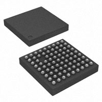
GQE (S-PBGA-N80)
PLASTIC BALL GRID ARRAY
5,10
SQ
4,90
4,00 TYP
0,50
J
0,50
H
G
F
E
D
C
B
A
1
0,68
0,62
2
3
4
5
6
7
8
9
1,00 MAX
Seating Plane
0,35
0,25
NOTES: A.
B.
C.
D.
∅ 0,05 M
0,21
0,11
0,08
4200461/C 10/00
All linear dimensions are in millimeters.
This drawing is subject to change without notice.
MicroStar Junior BGA configuration
Falls within JEDEC MO-225
MicroStar Junior is a trademark of Texas Instruments.
A–1
�PW (R-PDSO-G**)
PLASTIC SMALL-OUTLINE PACKAGE
14 PINS SHOWN
0,30
0,19
0,65
14
0,10 M
8
0,15 NOM
4,50
4,30
6,60
6,20
Gage Plane
0,25
1
7
0°– 8°
A
0,75
0,50
Seating Plane
0,15
0,05
1,20 MAX
PINS **
0,10
8
14
16
20
24
28
A MAX
3,10
5,10
5,10
6,60
7,90
9,80
A MIN
2,90
4,90
4,90
6,40
7,70
9,60
DIM
4040064/F 01/97
NOTES: A.
B.
C.
D.
A–2
All linear dimensions are in millimeters.
This drawing is subject to change without notice.
Body dimensions do not include mold flash or protrusion not to exceed 0,15.
Falls within JEDEC MO-153
�