User's Guide
SLAU280A – March 2009 – Revised October 2012
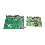
TLV320AIC36EVM-K
This user's guide describes the characteristics, operation, and use of the TLV320AIC36EVM-K. This
evaluation module (EVM) features a complete stereo audio codec with several inputs and outputs,
extensive audio routing, mixing, and effects capabilities. A complete circuit description, schematic
diagram, and bill of materials are also included.
The following related documents are available through the Texas Instruments Web site at www.ti.com.
EVM-Compatible Device Data Sheets
Device
Literature Number
TLV320AIC36
SBAS387
TAS1020B
SLES025
TPS767D318
SLVS209
SN74LVC125A
SCAS290
SN74LVC1G125
SCES223
SN74LVC1G07
SCES296
Contents
1
EVM Overview ............................................................................................................... 3
2
EVM Description and Basics .............................................................................................. 3
3
TLV320AIC36EVM-K Setup and Installation ............................................................................ 7
4
AIC36 Control Software .................................................................................................. 11
Appendix A
EVM Connector Descriptions ................................................................................... 29
Appendix B
TLV320AIC36EVM Schematic .................................................................................. 33
Appendix C TLV320AIC36EVM Layout Views .............................................................................. 34
Appendix D TLV320AIC36EVM Bill of Materials ............................................................................ 38
Appendix E
USB-MODEVM Schematic ...................................................................................... 40
Appendix F
USB-MODEVM Bill of Materials ................................................................................ 41
Appendix G USB-MODEVM Protocol ......................................................................................... 43
List of Figures
....................................................................................
1
TLV320AIC36EVM-K Block Diagram
2
Initial Screen of TLV320AIC36EVM-K Software ........................................................................ 9
3
Compatibility Tab .......................................................................................................... 10
4
Playback Script Tab ....................................................................................................... 12
5
Playback Panel ............................................................................................................ 13
6
Differential Microphone ................................................................................................... 14
7
Recording Panel ........................................................................................................... 14
8
DRC Information Tab
9
Program Codec Pop-Up Window ........................................................................................ 15
10
ADC Biquad Filter Tool ................................................................................................... 16
.....................................................................................................
4
15
I2S, I2C are trademarks of Koninklijke Philips Electronics N.V.
Windows is a trademark of Microsoft Corporation.
SPI is a trademark of Motorola, Inc.
I2C is a trademark of Philips Corporation.
SLAU280A – March 2009 – Revised October 2012
Submit Documentation Feedback
Copyright © 2009–2012, Texas Instruments Incorporated
TLV320AIC36EVM-K
1
�www.ti.com
11
DAC Biquad Filter Tool ................................................................................................... 18
12
Automatic Gain Control Panel ........................................................................................... 20
13
Dynamic Range Compression Panel ................................................................................... 21
14
Headset Detection Circuit ................................................................................................ 22
15
Headset Detection Panel ................................................................................................. 23
16
DC Measurement Panel .................................................................................................. 24
17
Audio Inputs Panel ........................................................................................................ 25
18
EEPROM Writer Panel.................................................................................................... 25
19
Status Flags Panel ........................................................................................................ 26
20
Register Tables Panel .................................................................................................... 27
21
Command-line Interface Panel
22
23
24
25
26
27
28
29
..........................................................................................
Top Layer ...................................................................................................................
Mid-Layer 1 .................................................................................................................
Mid-Layer 2 .................................................................................................................
Bottom Layer ...............................................................................................................
Top Overlay ................................................................................................................
Bottom Overlay ............................................................................................................
Drill Drawing ................................................................................................................
Composite ..................................................................................................................
28
34
34
35
35
36
36
37
37
List of Tables
1
USB-MODEVM SW2 Settings ............................................................................................. 5
2
List of Jumpers .............................................................................................................. 5
3
Jumper Settings for Headset Detection Example ..................................................................... 22
4
Analog Interface Pinout ................................................................................................... 29
5
Alternate Analog Connectors
6
Digital Interface Pinout .................................................................................................... 31
7
Power Supply Pin Out
8
9
2
............................................................................................
....................................................................................................
TLV320AIC36EVM Bill of Materials .....................................................................................
USB-MODEVM Bill of Materials .........................................................................................
TLV320AIC36EVM-K
30
32
38
41
SLAU280A – March 2009 – Revised October 2012
Submit Documentation Feedback
Copyright © 2009–2012, Texas Instruments Incorporated
�EVM Overview
www.ti.com
1
EVM Overview
1.1
Features
•
•
•
•
Full-featured evaluation board for the TLV320AIC36 stereo audio codec.
USB connection to PC provides power, control, and streaming audio data for easy evaluation.
Onboard microphone for ADC evaluation
Connection points for external control and digital audio signals for quick connection to other
circuits/input devices.
The TLV320AIC36EVM-K is a complete evaluation kit, which includes a universal serial bus (USB)-based
motherboard and evaluation software for use with a personal computer running Microsoft Windows™ XP.
1.2
Introduction
The TLV320AIC36EVM is in the Texas Instruments (TI) modular EVM form factor, which allows direct
evaluation of the device performance and operating characteristics and eases software development and
system prototyping.
The TLV320AIC36EVM-K is a complete evaluation/demonstration kit, which includes a USB-based
motherboard called the USB-MODEVM Interface board and evaluation software for use with a personal
computer (PC) running the Microsoft Windows XP operating system.
The TLV320AIC36EVM-K is operational with one USB cable connection to a PC. The USB connection
provides power, control, and streaming audio data to the EVM for reduced setup and configuration. The
EVM also allows external control signals, audio data, and power for advanced operation, which allows
prototyping and connection to the rest of the development or system evaluation.
2
EVM Description and Basics
This section provides information on the analog input and output, digital control, power, and general
connection of the TLV320AIC36EVM-K.
2.1
TLV320AIC36EVM-K Block Diagram
The TLV320AIC36EVM-K consists of two separate circuit boards, the USB-MODEVM and the
TLV320AIC36EVM. The USB-MODEVM is built around the TAS1020B streaming audio USB controller
with an 8051-based core. The motherboard features two positions for modular EVMs, or one double-wide
serial modular EVM can be installed. The TLV320AIC36EVM is one of the double-wide modular EVMs
that is designed to work with the USB-MODEVM.
The simple diagram of Figure 1 shows how the TLV320AIC36EVM is connected to the USB-MODEVM.
The USB-MODEVM Interface board is intended to be used in USB mode, where control of the installed
EVM is accomplished using the onboard USB controller device. Provision is made, however, for driving all
the data buses ( I2C™, SPI™, I2S, etc.) externally. The source of these signals is controlled by SW2 on
the USB-MODEVM. See Table 1 for details on the switch settings.
The USB-MODEVM has two EVM positions that allow for the connection of two small evaluation module
or one larger evaluation module. The TLV320AIC36EVM is designed to fit over both of the smaller
evaluation module slots as shown in Figure 1
SLAU280A – March 2009 – Revised October 2012
Submit Documentation Feedback
Copyright © 2009–2012, Texas Instruments Incorporated
TLV320AIC36EVM-K
3
�EVM Description and Basics
2.1.1
www.ti.com
USB-MODEVM Interface Board
The simple diagram of Figure 1 shows only the basic features of the USB-MODEVM Interface board.
Because the TLV320AIC36EVM is a double-wide modular EVM, it is installed with connections to both
EVM positions, which connects the TLV320AIC36 digital control interface to the I2C port realized using the
TAS1020B, as well as the TAS1020B digital audio interface.
In the factory configuration, the board is ready to be used with the USB-MODEVM. To view all the
functions and configuration options available on the USB-MODEVM board, see the USB-MODEVM
Interface Board schematic in Appendix G.
TLV320AIC36EVM
TLV320AIC36
USB-MODEVM
EVM Position 1
Control Interface
2
SPI, I C
TAS1020B
USB 8051
Microcontroller
EVM Position 2
USB
2
I S, AC97
Audio Interface
Figure 1. TLV320AIC36EVM-K Block Diagram
4
TLV320AIC36EVM-K
SLAU280A – March 2009 – Revised October 2012
Submit Documentation Feedback
Copyright © 2009–2012, Texas Instruments Incorporated
�EVM Description and Basics
www.ti.com
2.2
2.2.1
Default Configuration and Connections
USB-MODEVM
Table 1 provides a list of the SW2 settings on the USB-MODEVM. For use with the TLV320AIC36EVM,
SW-2 positions 1, 3, 4, 5, 6, and 7 must be set to ON, whereas SW-2.2 and SW-2.8 must be set to OFF. If
the TLV320AIC36EVM is to be used with an external audio interface, SW2.4 and SW2.5 also need to be
set to OFF and such interface must be connected as explained in Section 2.4
Table 1. USB-MODEVM SW2 Settings
SW-2 Switch Number
2.2.2
Label
Switch Description
1
A0
USB-MODEVM EEPROM I2C Address A0
ON: A0 = 0
OFF: A0 = 1
2
A1
USB-MODEVM EEPROM I2C Address A1
ON: A1 = 0
OFF: A1 = 1
3
A2
USB-MODEVM EEPROM I2C Address A2
ON: A2 = 0
OFF: A2 = 1
4
USB I2S
I2S Bus Source Selection
ON: I2S Bus connects to TAS1020
OFF: I2S Bus connects to USB-MODEVM J14
5
USB MCK
I2S Bus MCLK Source Selection
ON: MCLK connects to TAS1020
OFF: MCLK connects to USB-MODEVM J14
6
USB SPI
SPI Bus Source Selection
ON: SPI Bus connects to TAS1020
OFF: SPI Bus connects to USB-MODEVM J15
7
USB RST
RST Source Selection
ON: EVM Reset Signal comes from TAS1020
OFF: EVM Reset Signal comes from USB-MODEVM J15
8
EXT MCK
External MCLK Selection
ON: MCLK Signal is provided from USB-MODEVM J10
OFF: MCLK Signal comes from either selection of SW2-5
TLV320AIC36 Jumper Locations
Table 2 provides a list of jumpers found on the EVM and their factory default conditions.
Table 2. List of Jumpers
Jumper
Default
Position
W1
2-3
When connecting 2-3, microphone bias comes from the EXT_MICBIAS pin on the device; when connecting 1-2, microphone (mic)
bias is supplied by the AVDD_BIAS node. The AVDD_BIAS node can be sourced by two different supplies depending on the jumper
W13 setting or can be sourced by an external supply through TP34 (with W13 removed).
W2
Installed
Connects onboard Mic negative terminal to the circuit.
W3
Installed
Connects onboard Mic positive terminal to the circuit.
W4
Open
Connects the DETECT pin to J11.2.
W5
Installed
Provides mic bias to J11.2 through a 2.2kΩ equivalent resistance (W6 not installed) or 1kΩ resistor (W6 installed).
W6
Installed
Sets the mic bias resistance to 1 kΩ. Use for differential electret mic configurations.
W7
Installed
Connects J11.3 to the circuit.
W8
2-3
Connects J11.3 to ground or 1-kΩ resistor.
W9
Open
Connects a 1kΩ load to INT_MICBIAS.
W10
Installed
Connects HP_COM to ground.
W11
1-2
Connects AVDD_CP to the on-board regulator (U2) or an external +2.5V supply (through J18.3).
W12
1-2
Connects AVDD_REG to the on-board regulator (U2) or an external +2.5V supply (through J18.3).
W13
1-2
Connects AVDD_BIAS to the on-board regulator (U2) or an external +2.5V supply (through J18.3).
Jumper Description
SLAU280A – March 2009 – Revised October 2012
Submit Documentation Feedback
Copyright © 2009–2012, Texas Instruments Incorporated
TLV320AIC36EVM-K
5
�EVM Description and Basics
www.ti.com
Table 2. List of Jumpers (continued)
Jumper
Default
Position
Jumper Description
W14
1-2
Connects AVDD_ADC to AVDD2 or an external +1.8V supply (through J17.3).
W15
Open
Connects AVSS_REG to an external –2.5V supply (through J18.1). Do not connect if the charge pump is enabled.
W16
1-2
Connects AVDD_DAC to AVDD1 or an external +1.8V supply (through J17.3).
W17
1-2
Connects AVSS_DAC to AVSS1 or an external –1.8V supply (through J17.1).
W18
1-2
Connects AVDD_HP to AVDD1 or an external +1.8V supply (through J17.3).
W19
1-2
Connects AVSS_HP to AVSS1 or an external –1.8V supply (through J17.1).
W20
2-3
Connects I2C_ADDR0 to IOVDD or ground.
W21
2-3
Connects I2C_ADDR1 to IOVDD or ground.
W22
Open
Connects GPIO1 to J4.2/P4.2.
W23
Open
Connects GPIO2 to J4.6/P4.6.
W24
Installed
Provides a means of measuring IOVDD current.
W25
Installed
Provides a means of measuring DVDD current.
W26
1-2
Connects DVDD to +1.8VD (provided by P3.7/J3.7) or an external +1.8V supply (through J17.3).
W27
Open
Provides a means to connect IOVDD to +1.8VD (provided by P3.7/J3.7) or an external +1.8V supply (through J17.3).
W28
1-2
Connects IOVDD to +3.3VD (provided by P3.9/J3.9) or the source provided by the W27 setting.
W29
N/A
N/A
W30
Open
When installed, connects J4.8/P4.8 to RESETB.
W31
Installed
When installed, it selects onboard EEPROM as firmware source.
2.3
2.3.1
Analog Signal Connections
Analog Inputs
The analog input sources can be applied directly to terminal blocks J7, J8, J9 and J10 or input jacks J6
and J11. The connection details can be found in Appendix A.
2.3.2
Analog Output
The analog outputs are available from terminal blocks J13, J14, J15 and J16 or output jack J12. The
connection details can be found in Appendix A.
2.4
Digital Signal Connections
The digital inputs and outputs of the EVM can be monitored through P4 and P5. If external signals need to
be connected to the EVM, digital inputs must be connected via J14 and J15 on the USB-MODEVM and
the SW2 switch must be changed accordingly (see Section 2.2.1). The connector details are available in
Section A.2.
2.5
Power Connections
The TLV320AIC36EVM can be powered independently when being used in stand-alone operation or by
the USB-MODEVM when it is plugged onto the motherboard.
6
TLV320AIC36EVM-K
SLAU280A – March 2009 – Revised October 2012
Submit Documentation Feedback
Copyright © 2009–2012, Texas Instruments Incorporated
�TLV320AIC36EVM-K Setup and Installation
www.ti.com
2.5.1
Stand-Alone Operation
When used as a stand-alone EVM, power is applied to P3/J3 directly, making sure to reference the
supplies to the appropriate grounds on that connector.
CAUTION
Verify that all power supplies are within the safe operating limits shown on the
TLV320AIC36 data sheet before applying power to the EVM.
P3/J3 provides connection to the common power bus for the TLV320AIC36EVM. Power is supplied on the
pins listed in Table 7.
The TLV320AIC36EVM-K motherboard (the USB-MODEVM Interface board) supplies power to J3 of the
TLV320AIC36EVM. Power for the motherboard is supplied either through its USB connection or via
terminal blocks on that board.
2.5.2
USB-MODEVM Operation
The USB-MODEVM Interface board can be powered from several different sources:
• USB
• 6-Vdc to 10-Vdc AC/DC external wall supply (not included)
• Laboratory power supply
When powered from the USB connection, JMP6 must have a shunt from pins 1–2 (this is the default
factory configuration). When powered from 6-Vdc to 10-Vdc power supply, either through the J8 terminal
block or J9 barrel jack, JMP6 must have a shunt installed on pins 2–3. If power is applied in any of these
ways, onboard regulators generate the required supply voltages, and no further power supplies are
necessary.
If laboratory supplies are used to provide the individual voltages required by the USB-MODEVM Interface,
JMP6 must have no shunt installed. Voltages are then applied to J2 (+5VA), J3 (+5VD), J4 (+1.8VD), and
J5 (+3.3VD). The +1.8VD and +3.3VD can also be generated on the board by the onboard regulators from
the +5VD supply; to enable this configuration, the switches on SW1 need to be set to enable the
regulators by placing them in the ON position (lower position, looking at the board with text reading rightside up). If +1.8VD and +3.3VD are supplied externally, disable the onboard regulators by placing SW1
switches in the OFF position.
Each power supply voltage has an LED (D1-D7) that illuminates when the power supplies are active.
3
TLV320AIC36EVM-K Setup and Installation
The following section provides information on using the TLV320AIC36EVM-K, including setup, program
installation, and program usage.
NOTE: If using the EVM in stand-alone mode, the software must be installed per the following
instructions, but the hardware configuration may be different.
3.1
Software Installation
1. Download the latest version of the AIC36 Control Software (CS) located in the TLV320AIC36EVM-K
Product Folder.
2. Open the self-extracting installation file.
3. Extract the software to a known folder.
4. Install the EVM software by double-clicking the Setup executable, and follow the directions. The user
may be prompted to restart their computer.
This installs all the TLV320AIC36EVM-K software.
SLAU280A – March 2009 – Revised October 2012
Submit Documentation Feedback
Copyright © 2009–2012, Texas Instruments Incorporated
TLV320AIC36EVM-K
7
�TLV320AIC36EVM-K Setup and Installation
3.2
www.ti.com
EVM Connections
1. Ensure that the TLV320AIC36EVM is installed on the USB-MODEVM Interface board, aligning J1, J2,
J3, J4, and J5 with the corresponding connectors on the USB-MODEVM.
2. Verify that the jumpers and switches are in their default conditions.
3. Attach a USB cable from the PC to the USB-MODEVM Interface board. The default configuration
provides power, control signals, and streaming audio via the USB interface from the PC. On the USBMODEVM, LEDs D3, D4, D5, and D7 illuminate to indicate that the USB is supplying power.
4. For the first connection, the PC recognizes new hardware and begins an initialization process. The
TLV320AIC36EVM-K will enumerate as a "USB Human Interface Device" and as a "USB Audio
Device".
5. Once the PC confirms that the hardware is operational, D2 on the USB-MODEVM illuminates to
indicate that the firmware has been loaded and the EVM is ready for use. If D2 does not illuminate,
verify that the EEPROM jumper and switch settings conform to Table 1 and Table 2.
After the TLV320AIC36EVM-K software installation (described in Section 3.2) is complete, evaluation and
development with the TLV320AIC36 can begin.
8
TLV320AIC36EVM-K
SLAU280A – March 2009 – Revised October 2012
Submit Documentation Feedback
Copyright © 2009–2012, Texas Instruments Incorporated
�TLV320AIC36EVM-K Setup and Installation
www.ti.com
The TLV320AIC36EVM-K software can now be launched. The user sees an initial screen that looks
similar to Figure 2.
Figure 2. Initial Screen of TLV320AIC36EVM-K Software
SLAU280A – March 2009 – Revised October 2012
Submit Documentation Feedback
Copyright © 2009–2012, Texas Instruments Incorporated
TLV320AIC36EVM-K
9
�TLV320AIC36EVM-K Setup and Installation
www.ti.com
If running the software in Windows Vista or Windows 7, right-click the AIC36EVM-K CS shortcut and
select Properties. Configure the Compatibility tab as shown in Figure 3
Figure 3. Compatibility Tab
10
TLV320AIC36EVM-K
SLAU280A – March 2009 – Revised October 2012
Submit Documentation Feedback
Copyright © 2009–2012, Texas Instruments Incorporated
�AIC36 Control Software
www.ti.com
4
AIC36 Control Software
The AIC36 Control Software (CS) is an intuitive, easy-to-use, powerful tool to learn, evaluate, and control
the TLV320AIC36. This tool was specifically designed to make learning the TLV320AIC36 easy. The
following sections describe the operation of this software.
NOTE: For configuration of the codec, the TLV320AIC36 block diagram located in the TLV320AIC36
data sheet is a good reference to help determine the signal routing.
4.1
Main Panel Window
The Main Panel window, shown in Figure 2, provides easy access to all the features of the AIC36 CS. The
Firmware Name and Version boxes provide information about the firmware loaded into the EVM's
EEPROM.
The USB Interface drop-down menu allows the user to select which communication protocol the
TAS1020B USB Controller uses to communicate with the TLV320AIC36 or to toggle the TAS1020B GPIO
pins. The USB-MODEVM Interface selection is global to all panels, including the Command-Line Interface.
The I2C Address box sets the global I2C address to be used by controls and indicators. Note that scripts
executed in the command line interface and in other panels use the I2C address provided in each
command and not the global I2C address.
The Panel Selection Tree provides access to typical configurations, features, and other panels that allow
the user to control the TLV320AIC36. The tree is divided into several categories which contain items that
pop up panels. A panel can be opened by double-clicking any item inside a category in the Panel
Selection Tree.
Below the Panel Selection Tree are three buttons that pop up the following:
•
•
•
Status Flags - Allows the user to monitor the TLV320AIC36 status flags.
Register Tables - A tool to monitor register pages.
Command-Line Interface - A tool to execute/generate scripts and monitor register activity.
The USB LED indicates if the EVM kit is recognized by the software and the ACTIVITY LED illuminates
every time a command request is sent.
The dialog box at the bottom of the Main Panel provides feedback of the current status of the software.
For USB-MODEVM firmware versions 2.01 and above, it is possible to update the firmware on-the-fly.
This is useful for cases in which different USB Audio sampling rates are desired, or when a new firmware
version is released. The "USB Audio Sampling Rate" dialog box displays the current USB audio sampling
rate supported by a particular firmware. Details on how to re-program the firmware are available in Section
4.1.4.
SLAU280A – March 2009 – Revised October 2012
Submit Documentation Feedback
Copyright © 2009–2012, Texas Instruments Incorporated
TLV320AIC36EVM-K
11
�AIC36 Control Software
4.1.1
www.ti.com
Typical Configurations
This category can help users to quickly become familiar with the TLV320AIC36. Each of the panels that
can be accessed through this menu have controls relevant to the selected configuration; a tab shows the
script that will be loaded for that particular configuration. Each script includes a brief description of the
selected configuration, as shown in Figure 4.
Figure 4. Playback Script Tab
4.1.1.1
Playback
The Playback panel (shown in Figure 5) has the following configurations:
• Stereo DAC Playback - this configuration programs the TLV320AIC36 for stereo playback through the
headphone outputs. The DAC is also connected to the line and receiver driver mixers but are powered
down and muted by default.
• Stereo ADC Record and DAC Playback - this configuration is the same as Stereo DAC Playback, but
with the LINEIN inputs connected to the ADC.
• LINEIN Analog Bypass - this configuration routes LINEIN to all output mixers. Only the HP outputs are
powered and unmuted.
• PGA Analog Bypass - this configuration routes LINEIN to the analog input amplifier (Mic PGA) which is
then routed all output mixers. Only the HP outputs are powered and unmuted.
The analog inputs and outputs used for these configurations can be accessed as follows:
1.
2.
3.
4.
12
Line inputs - Jack J6 or terminal block J7.
Line outputs - Terminal blocks J14 and J15.
Receiver outputs - Terminal block J16.
Headphone outputs - Jack J12. A filtered version is available at J13 (for high impedance loads only).
TLV320AIC36EVM-K
SLAU280A – March 2009 – Revised October 2012
Submit Documentation Feedback
Copyright © 2009–2012, Texas Instruments Incorporated
�AIC36 Control Software
www.ti.com
Figure 5. Playback Panel
4.1.1.2
Recording
The Recording panel (shown in Figure 7) has the following configurations:
• Stereo ADC Recording - LINEIN_L and LINEIN_R are routed to the left ADC and right ADC,
respectively, in a single ended fashion.
• Differential On-Board Mic - The on-board microphone is routed to EXTMIC and to the left ADC. The
jumper settings for this configuration are shown in Figure 6.
The analog inputs used for these configurations can be accessed as follows:
1. Line inputs - Jack J6 or terminal block J7.
SLAU280A – March 2009 – Revised October 2012
Submit Documentation Feedback
Copyright © 2009–2012, Texas Instruments Incorporated
TLV320AIC36EVM-K
13
�AIC36 Control Software
www.ti.com
INPUT TYPE
MODE
DIFFERENTIAL
MONO
CODEC
INPUTS
EXTMIC_P
EXTMIC_M
ONBOARD MIC
JUMPERS
W2
W3
IN
IN
INPUT CONFIG
JUMPER
SETTINGS
W5
W6
W7
W8
IN
IN
IN
2-3
Figure 6. Differential Microphone
Figure 7. Recording Panel
4.1.2
Features
The Features category allows the user to evaluate various features of the TLV320AIC36. Each of the
Features panels include an Information tab that explains the feature and provides hardware setup
information for easy evaluation, as seen in Figure 8.
14
TLV320AIC36EVM-K
SLAU280A – March 2009 – Revised October 2012
Submit Documentation Feedback
Copyright © 2009–2012, Texas Instruments Incorporated
�AIC36 Control Software
www.ti.com
Figure 8. DRC Information Tab
Any item in the Features category can be accessed by a double-click. As soon as a Features panel
opens, a pop-up message appears asking to program the codec for that feature (see Figure 9). A
command script is sent to the codec if the OK button is clicked. This script programs all registers
necessary to evaluate the feature. This can be bypassed by clicking the Cancel button.
Figure 9. Program Codec Pop-Up Window
The script corresponding to each feature can be accessed at the [Installation Directory]\DATA\EVM folder.
Also, each script can be manually customized and loaded as the feature's start-up script as long as the file
name remains the same.
SLAU280A – March 2009 – Revised October 2012
Submit Documentation Feedback
Copyright © 2009–2012, Texas Instruments Incorporated
TLV320AIC36EVM-K
15
�AIC36 Control Software
4.1.2.1
www.ti.com
ADC Biquad Filter Tool
The ADC Biquad Filter Tool allows the user to specify the following biquad filters downloadable to the
TLV320AIC36:
- All-pass
- High-pass (Butterworth first-order, Butterworth second-order, Bessel second-order, Linkwitz-Riley
second-order, and variable-Q second-order)
- Low-pass (Butterworth first-order, Butterworth second-order, Bessel second-order, Linkwitz-Riley
second-order, and variable-Q second-order)
- EQ (equalizer)
- Notch
- Treble shelf
- Bass shelf
Figure 10. ADC Biquad Filter Tool
To use the default EVM settings with the Biquad Filter Tool click on the "Recording" application and
download for example the line-input script to setup EVM for line-in recording then proceed to use the
Biquad Filter Tool.
Step 1: Select the Processing Block - This specifies the number of biquads available (3 or 5) and stereo or
mono (right). For best results use Processing Block PRB_R2 as this works well with the default EVM
setup.
16
TLV320AIC36EVM-K
SLAU280A – March 2009 – Revised October 2012
Submit Documentation Feedback
Copyright © 2009–2012, Texas Instruments Incorporated
�AIC36 Control Software
www.ti.com
Step 2: Specify the Sample Rate - This is a key design parameter input to the Biquad Tool. The default is
44.1kHz which is the sample rate used on the EVM. The tool will work with any sample rate from 8kHz to
96kHz, however, if a sample rate other than 44.1kHz is selected then the user must go the the clock panel
to modify the PLL and/or clock settings so that the desired sample rate is setup properly when used with
an external audio interface.
Step 3: Specify the Biquad Filters - Select the filter type and subtype and enter any required parameters.
Note that the parameters not used will be grayed out. Use the "Plot" Check-Box to select the filters to plot
and/or download.
Step 4: Calculate the Coefficients - Click on the "Calculate Coefficients" OK button. This calculates all the
selected filters and plots the combined response of all the checked filters. If a filter is not checked it is
treated as an All-Pass filter.
Step 5: Inspect the Plots - Based on the selected filters determine if this is the total desired response.
Also, inspect the Scale (dB) display. Some filters may create a negative gain error which is reflected in the
scale. For example, if the Scale displays 0.5 there is a - 0.5dB gain error which can be corrected in the
analog PGA or the digital Volume. In the last column the stability of the filter is indicated. If the roots of the
filter denominator are less than 1 then the filter is stable and this field will display the text "Stable".
Otherwise, it will display the text "Unstable" meaning that the unstable filter should be re-specified until it is
stable.
Step 6: Download the Coefficients - Click on the "Download Coefficients" OK button. This action will
download the filter coefficients to the device. Note that in order to download coefficients into the device,
the following register writes are done:
1. Page 0 - Select processing block and Power-Down both ADCs
2. Page 4 - Write filter coefficients to both left and right channels as required
3. Page 0 - Power-Up both ADCs
Note that the filter coefficients can be saved as an I2C script by using the Command-Line Interface
Record Button. The I2C commands will be displayed in the Command Buffer which can be selected and
copied to a text command file.
4.1.2.2
DAC Biquad Filter Tool
The DAC Biquad Filter Tool allows the user to specify the following biquad filters downloadable to the
TLV320AIC36:
- All-pass
- High-pass (Butterworth first-order, Butterworth second-order, Bessel second-order, Linkwitz-Riley
second-order, and variable-Q second-order)
- Low-pass (Butterworth first-order, Butterworth second-order, Bessel second-order, Linkwitz-Riley
second-order, and variable-Q second-order)
- EQ (equalizer)
- Notch
- Treble shelf
- Bass shelf
SLAU280A – March 2009 – Revised October 2012
Submit Documentation Feedback
Copyright © 2009–2012, Texas Instruments Incorporated
TLV320AIC36EVM-K
17
�AIC36 Control Software
www.ti.com
Figure 11. DAC Biquad Filter Tool
To test the filters with USB Audio, select a configuration from the 'Typical Configurations>Playback' panel.
The 'Stereo DAC Playback' configuration is optimized for any 'Filter A' processing block. Alternatively, a
custom script can be loaded into the Command-Line Interface panel before downloading coefficients. This
tool assumes that Adaptive Filtering is enabled for real-time filtering.
Step 1: Select the Processing Block - This specifies the number of biquads available and stereo or mono
(left). For best results, use Processing Block PRB_P2 as this works well with the default EVM setup. To
change the processing block on the device:
1. Go to the 'Analog Settings>Audio Outputs' panel to uncheck the 'Enable DACs' box.
2. Go to the 'Signal Processing>Processing Blocks' panel to select the DAC processing block.
3. Go to the 'Analog Settings>Audio Outputs' panel to check the 'Enable DACs' box.
Step 2: Specify the Sample Rate - This is a key design parameter input to the Biquad Tool. The default is
44.1kHz which is the sample rate used on the EVM. The tool will work with any sample rate from 8kHz to
96kHz, however, if a sample rate other than 44.1kHz is selected then the user must go the the clock panel
to modify the PLL and/or clock settings so that the desired sample rate is setup properly when used with
an external audio interface.
18
TLV320AIC36EVM-K
SLAU280A – March 2009 – Revised October 2012
Submit Documentation Feedback
Copyright © 2009–2012, Texas Instruments Incorporated
�AIC36 Control Software
www.ti.com
Step 3: Specify the Biquad Filters - Select the filter type and subtype and enter any required parameters.
Note that the parameters not used will be grayed out. Use the "Plot" Check-Box to select the filters to plot
and/or download.
Step 4: Calculate the Coefficients - Click on the "Calculate Coefficients" OK button. This calculates all the
selected filters and plots the combined response of all the checked filters. If a filter is not checked it is
treated as an All-Pass filter.
Step 5: Inspect the Plots - Based on the selected filters determine if this is the total desired response.
Also, inspect the Scale (dB) display. Some filters may create a negative gain error which is reflected in the
scale. For example, if the Scale displays 0.5 there is a - 0.5dB gain error which can be corrected with the
Digital PGA and amplifier gain. In the last column the stability of the filter is indicated. If the roots of the
filter denominator are less than 1 then the filter is stable and this field will display the text "Stable".
Otherwise, it will display the text "Unstable" meaning that the unstable filter should be re-specified until it is
stable.
Step 6: Download the Coefficients - Click on the "Download Coefficients" OK button. This action will
download the filter coefficients to the device. Note that in order to download coefficients into the device,
the following register writes are done:
1. Page 8 - Write filter coefficients to both left and right channels as required
2. Page 8 - Switch Buffers and wait for flag to clear.
3. Page 8 - Re-write filter coefficients to both left and right channels as required
Note that the filter coefficients can be saved as an I2C script by using the Command-Line Interface
Record Button. The I2C commands will be displayed in the Command Buffer which can be selected and
copied to a text command file.
4.1.2.3
Automatic Gain Control
The left-channel Automatic Gain Control (AGC) can be enabled by checking the Enable Left AGC box
(Figure 12). Pressing the Capture Audio button records the left-channel audio. Its corresponding data is
displayed in the audio capture graph window. The small white window located at the bottom right of the
AGC tab displays the audio waveform of the recorded data. Ensure that the AIC32x4 EVM is selected as
the computer's default audio capture device before pressing this button. To set the TLV320AIC36EVM-K
as the default audio device, open the Windows™ Control Panel → Sounds and Audio Devices Properties
and set the AIC32x4 EVM as the default audio recording device. Also, do not use any other media player
or audio recording software while the control software is recording.
The target level and noise threshold parameters can be modified by dragging the horizontal cursor lines
located at the audio capture graph window. Its numeric values are displayed to the right of the graph.
Noise threshold can be disabled by unchecking the Enable Noise Threshold box. The AGC Max Gain
control sets the maximum allowed AGC PGA Gain. The AGC Gain indicator bar continuously displays the
contents of Page 0/Register 93 if the Enable Polling box is checked.
Other parameters can be accessed by checking the Advanced box. For more information about AGC, see
the Information tab and the data sheet.
Other flags related to this feature can be accessed at the Status Flags panel.
SLAU280A – March 2009 – Revised October 2012
Submit Documentation Feedback
Copyright © 2009–2012, Texas Instruments Incorporated
TLV320AIC36EVM-K
19
�AIC36 Control Software
www.ti.com
Figure 12. Automatic Gain Control Panel
4.1.2.4
Dynamic Range Compression
Dynamic Range Compression (DRC) can be enabled by checking the Enable Left DRC and Enable
Right DRC boxes.
The level transfer characteristic graph is a function of the applied digital gain and the threshold parameter.
The graph line is separated into two piece-wise linear regions where the red line represents the level
range in which the DRC attenuation takes place, and the green line represents the level range in which
the signal is not affected by DRC. As an example, setting the threshold to -24 dB with a gain to 24 dB
implies that an input signal strength variation from -48 dB (threshold - gain) to 0 dB results in an output
signal strength variation from -24 dB to 0 dB, or a compression ratio of 2:1. Similarly, a threshold of -3 dB
with a gain of 24 dB implies that an input signal strength variation from -27 dB to 0 dB results in an output
signal strength variation from -3 dB to 0 dB, or a ratio of 9:1. Note that a gain less than 0 dB does not
result in expansion.
The Attack and Decay are time domain parameters that control the rate in which the applied gain reaches
the target gain after the threshold level is crossed. As an example, a fast attack rate quickly reaches the
target gain once the output signal crosses the programmed threshold region.
Other flags related to this feature can be accessed at the Status Flags panel.
20
TLV320AIC36EVM-K
SLAU280A – March 2009 – Revised October 2012
Submit Documentation Feedback
Copyright © 2009–2012, Texas Instruments Incorporated
�AIC36 Control Software
www.ti.com
Figure 13. Dynamic Range Compression Panel
4.1.2.5
Headset Detection
Screw terminal J10 (EXT MIC IN) is provided to connect an external microphone, as well as unique push
button combinations. As an example, the circuit shown below, connects a push button-resistor
combination.
SLAU280A – March 2009 – Revised October 2012
Submit Documentation Feedback
Copyright © 2009–2012, Texas Instruments Incorporated
TLV320AIC36EVM-K
21
�AIC36 Control Software
www.ti.com
J10
1
2
R1
R2
3
EXT MIC IN
Figure 14. Headset Detection Circuit
This circuit can be used in combination with the on-board differential microphone (MK1) by using the
following jumper settings:
Table 3. Jumper Settings for Headset Detection Example
Jumper
22
Setting
W1
2-3
W2
Inserted
W3
Inserted
W4
Inserted
W5
Inserted
W6
Open
W7
Inserted
W8
1-2
TLV320AIC36EVM-K
SLAU280A – March 2009 – Revised October 2012
Submit Documentation Feedback
Copyright © 2009–2012, Texas Instruments Incorporated
�AIC36 Control Software
www.ti.com
The DETECT SAR section in the image below shows a result of 19 as its Raw detect value. The
WINDOW COMPARATOR section is configured for three windows separated by two threshold levels:
window 0 (bits 0 to 13), window 1 (bits 14 to 27) and window 2 (bits 28 to 31). The detected window is
"window 1" (raw detect value of 19) as shown in the PULSE DETECT sections.
Figure 15. Headset Detection Panel
The Enable Polling button must be checked in order to update all dialog boxes, even if continuous mode
or a single read is used.
4.1.2.6
DC Measurement
Terminal block J3 on the TLV320AIC36EVM can be used to evaluate the DC measurement feature. The
Information tab provides the hardware setup information.
The Left ADC (V) and Right ADC (V) boxes convert the register data to voltage. The voltage is derived
from the References shown at the upper right corner of the DC Measurement tab. The DC measurement
register data is in 2.22, 2s complement format.
Checking the Enable Polling box displays the DC measurement data.
Other flags related to this feature can be accessed at the Status Flags panel.
SLAU280A – March 2009 – Revised October 2012
Submit Documentation Feedback
Copyright © 2009–2012, Texas Instruments Incorporated
TLV320AIC36EVM-K
23
�AIC36 Control Software
www.ti.com
Figure 16. DC Measurement Panel
4.1.3
Control Categories
The Digital Settings, Analog Settings, and Signal Processing categories provide control of many
registers and other features of the TLV320AIC36 . These categories are intended for the advanced user.
Hovering the mouse cursor on top of a control displays a tip strip that contains page, register, and bit
information. As an example, hovering on top of an input in the Audio Inputs panel, as shown in Figure 17
displays p1_r55_b7-6 which means that this control writes to Page 1/Register 55/Bits D7 to D6.
24
TLV320AIC36EVM-K
SLAU280A – March 2009 – Revised October 2012
Submit Documentation Feedback
Copyright © 2009–2012, Texas Instruments Incorporated
�AIC36 Control Software
www.ti.com
Figure 17. Audio Inputs Panel
All
•
•
•
4.1.4
controls update their status with respect to the register contents in the following conditions:
A panel is opened.
The Execute Command Buffer button in the Command-Line Interface is pressed.
The Refresh button at the bottom right of a panel is pressed.
EEPROM Writer
The EEPROM Writer allows the user to upgrade the firmware used by the TAS1020B USB Controller.
More information about this panel can be found by double-clicking the "Tools > EEPROM Writer" item, as
shown below.
Figure 18. EEPROM Writer Panel
SLAU280A – March 2009 – Revised October 2012
Submit Documentation Feedback
Copyright © 2009–2012, Texas Instruments Incorporated
TLV320AIC36EVM-K
25
�AIC36 Control Software
4.2
www.ti.com
Status Flags Panel
The TLV320AIC36 status flags can monitored in the Status Flags panel (Figure 19) which is located
below the Panel Selection Tree . Pressing the POLL button continuously reads all the registers relevant
to each flag and updates those flags accordingly. The rate at which the registers are read can be modified
by chang
ing the value in the Polling Interval numeric control. Note that a smaller interval reduces responsiveness
of other controls, especially volume sliders, due to bandwidth limitations. By default, the polling interval is
200 ms and can be set to a minimum of 20 ms.
The Sticky Flags tab contains indicators whose corresponding register contents clear every time a read is
performed to that register. To read all the sticky flags, click the Read Sticky Flags button.
Figure 19. Status Flags Panel
4.3
Register Tables Panel
The contents of configuration and coefficient pages of the TLV320AIC36 can be accessed through the
Register Tables panel (Figure 20).
The Page Number control changes to the page to be displayed in the register table. The register table
contains page information such as the register name, reset value, current value, and a bitmap of the
current value. The contents of the selected page can be exported into a spreadsheet by clicking the Dump
to Spreadsheet button.
26
TLV320AIC36EVM-K
SLAU280A – March 2009 – Revised October 2012
Submit Documentation Feedback
Copyright © 2009–2012, Texas Instruments Incorporated
�AIC36 Control Software
www.ti.com
Figure 20. Register Tables Panel
4.4
Command-Line Interface Panel
The Command-Line Interface panel provides a means to communicate with the TLV320AIC36 using a
simple scripting language (described in Section G.1). The TAS1020B USB Controller (located on the USBMODEVM motherboard) handles all communication between the PC and the TLV320AIC36.
A script is loaded into the command buffer, either by loading a script file using the File menu or by pasting
text from the clipboard using the Ctrl-V key combination (Figure 21).
When the command buffer is executed, the return data packets which result from each individual
command are displayed in the Command History control. This control is an array (with a maximum size
of 100 elements) that contains information about each command as well as status. The Interface box
displays the interface used for a particular command in the Command History array. The Command box
displays the type of command executed (i.e., write, read) for a particular interface. The Flag Retries box
displays the number of read iterations performed by a Wait for Flag command (see Section G.1 for
details). The Register Data array displays the register number and data bytes that correspond to a
particular command.
The Information tab provides additional information related to the Command History as well as
additional settings. The Syntax and Examples tabs provide useful information related to the scripting
language.
The File menu provides some options for working with scripts. The first option, Open Script File..., loads a
command file script into the command buffer. This script can then be executed by pressing the Execute
Command Buffer button. The contents of the Command Buffer can be saved using the Save Script
File... option.
Both the Command Buffer and Command History can be cleared by clicking their corresponding Clear
buttons.
The Record button generates script commands based on data written by other panels.
SLAU280A – March 2009 – Revised October 2012
Submit Documentation Feedback
Copyright © 2009–2012, Texas Instruments Incorporated
TLV320AIC36EVM-K
27
�AIC36 Control Software
www.ti.com
Figure 21. Command-line Interface Panel
28
TLV320AIC36EVM-K
SLAU280A – March 2009 – Revised October 2012
Submit Documentation Feedback
Copyright © 2009–2012, Texas Instruments Incorporated
�www.ti.com
Appendix A EVM Connector Descriptions
This appendix contains the connection details for each of the main connectors on the EVM.
A.1
Analog Interface Connectors
A.1.1
Analog Dual-Row Socket Details, J1 and J2
The TLV320AIC36EVM has two analog dual-row sockets located at the bottom of the board. These
sockets provide support to the EVM and connect the analog ground plane of the EVM to the USBMODEVM analog ground. Consult Samtec at www.samtec.com or call 1-800-SAMTEC-9 for a variety of
mating connector options. Table 4 summarizes the analog interface pinout for the TLV320AIC36EVM.
Table 4. Analog Interface Pinout
PIN NUMBER
SIGNAL
DESCRIPTION
J1.1
NC
Not Connected
J1.2
NC
Not Connected
J1.3
NC
Not Connected
J1.4
NC
Not Connected
J1.5
NC
Not Connected
J1.6
NC
Not Connected
J1.7
NC
Not Connected
J1.8
NC
Not Connected
J1.9
AGND
Analog Ground
J1.10
NC
Not Connected
J1.11
AGND
Analog Ground
J1.12
NC
Not Connected
J1.13
AGND
Analog Ground
J1.14
NC
Not Connected
J1.15
NC
Not Connected
J1.16
NC
Not Connected
J1.17
AGND
Analog Ground
J1.18
NC
Not Connected
J1.19
AGND
Analog Ground
J1.20
NC
Not Connected
J2.1
NC
Not Connected
J2.2
NC
Not Connected
J2.3
NC
Not Connected
J2.4
NC
Not Connected
J2.5
NC
Not Connected
J2.6
NC
Not Connected
J2.7
NC
Not Connected
J2.8
NC
Not Connected
J2.9
AGND
Analog Ground
J2.10
NC
Not Connected
J2.11
AGND
Analog Ground
J2.12
NC
Not Connected
J2.13
AGND
Analog Ground
J2.14
NC
Not Connected
J2.15
NC
Not Connected
J2.16
NC
Not Connected
J2.17
AGND
Analog Ground
J2.18
NC
Not Connected
J2.19
AGND
Analog Ground
SLAU280A – March 2009 – Revised October 2012
Submit Documentation Feedback
Copyright © 2009–2012, Texas Instruments Incorporated
EVM Connector Descriptions
29
�Analog Interface Connectors
www.ti.com
Table 4. Analog Interface Pinout (continued)
A.1.2
PIN NUMBER
SIGNAL
DESCRIPTION
J2.20
NC
Not Connected
Analog Screw Terminal and Audio Jack Details, J6 to J18
The analog inputs and outputs can be accessed through screw terminals or audio jacks. Also, provision is
made to connect power supply sources to screw terminals.
Table 5 summarizes the screw terminals and audio jacks available on the TLV320AIC36EVM.
Table 5. Alternate Analog Connectors
DESIGN
ATOR
PIN 1
PIN 2
J6 (LINE
IN)
AGND
LINEIN_L LINEIN_R NC
J7 (LINE
IN)
LINEIN_R
AGND
LINEIN_L
J8 (MIC 1 MIC1_P
IN)
AGND
MIC1_M
J9 (MIC 2 MIC2_P
IN)
AGND
MIC2_M
J10 (EXT
MIC IN)
EXTMIC_
P / NC
AGND
EXTMIC_
M / NC
J11 (EXT
MIC IN)
AGND
EXTMIC_ EXTMIC_ EXTMIC
P
M
_P / NC
EXTMIC_M /
NC
J12
HP_COM
(HEADSE
T
OUTPUT)
HPL
HPR / NC
J13
HPL / NC
(HP_FILT
)
HP_COM HPR / NC
J14
(LO_LEF
T)
LINEOUT
_LP
LINEOUT
_LM
J15
(LO_RIG
HT)
LINEOUT
_RP
LINEOUT
_RP
J16
RECL
(REC_OU
T)
30
EVM Connector Descriptions
AGND
PIN3
HPR
PIN4
HPL /
NC
PIN5
NC
RECR
SLAU280A – March 2009 – Revised October 2012
Submit Documentation Feedback
Copyright © 2009–2012, Texas Instruments Incorporated
�Digital Interface Connectors, P4/J4 and P5/J5
www.ti.com
A.2
Digital Interface Connectors, P4/J4 and P5/J5
The TLV320AIC36EVM is designed to easily interface with multiple control platforms. Samtec part
numbers SSW-110-22-F-D-VS-K and TSM-110-01-T-DV-P provide a convenient 10-pin, dual-row
header/socket combination at P4/J4 and P5/J5. These headers/sockets provide access to the digital
control and serial data pins of the device. Consult Samtec at www.samtec.com or call 1-800- SAMTEC-9
for a variety of mating connector options. Table 6 summarizes the digital interface pinout for the
TLV320AIC36EVM.
Table 6. Digital Interface Pinout
PIN NUMBER
SIGNAL
DESCRIPTION
P4.1/J4.1
NC
Not Connected
P4.2/J4.2
NC
Not Connected
P4.3/J4.3
NC
Not Connected
P4.4/J4.4
DGND
Digital Ground
P4.5/J4.5
NC
Not Connected
P4.6/J4.6
NC
Not Connected
P4.7/J4.7
NC
Not Connected
P4.8/J4.8
RESET
TAS1020B Reset
P4.9/J4.9
NC
Not Connected
P4.10/J4.10
DGND
Digital Ground
P4.11/J4.11
NC
Not Connected
P4.12/J4.12
NC
Not Connected
P4.13/J4.13
NC
Not Connected
P4.14/J4.14
RESET
TAS1020B Reset
P4.15/J4.15
NC
Not Connected
P4.16/J4.16
NC
Not Connected
P4.17/J4.17
NC
Not Connected
P4.18/J4.18
DGND
Digital Ground
P4.19/J4.19
NC
Not Connected
P4.20/J4.20
NC
Not Connected
P5.1/J5.1
NC
Not Connected
P5.2/J5.2
NC
Not Connected
P5.3/J5.3
BCLK
Audio Serial Data Bus Bit Clock (Input/Output)
P5.4/J5.4
DGND
Digital Ground
P5.5/J5.5
NC
Not Connected
P5.6/J5.6
NC
Not Connected
P5.7/J5.7
WCLK
Audio Serial Data Bus Word Clock (Input/Output)
P5.8/J5.8
NC
Not Connected
P5.9/J5.9
NC
Not Connected
P5.10/J5.10
DGND
Digital Ground
P5.11/J5.11
DIN
Audio Serial Data Bus Data Input (Input)
P5.12/J5.12
NC
Not Connected
P5.13/J5.13
DOUT
Audio Serial Data Bus Data Output (Output)
P5.14/J5.14
NC
Not Connected
P5.15/J5.15
NC
Not Connected
P5.16/J5.16
SCL
I2C Serial Clock
P5.17/J5.17
MCLK
Master Clock Input
P5.18/J5.18
DGND
Digital Ground
P5.19/J5.19
NC
Not Connected
P5.20/J5.20
SDA
I2C Serial Data Input/Output
SLAU280A – March 2009 – Revised October 2012
Submit Documentation Feedback
Copyright © 2009–2012, Texas Instruments Incorporated
EVM Connector Descriptions
31
�Power Supply Connector Pin Header, P3/J3
www.ti.com
Note that P5/J5 comprises the signals needed for an I2S™ serial digital audio interface and the control
interface ( I2C™).
A.3
Power Supply Connector Pin Header, P3/J3
P3/J3 provides connection to the common power bus for the TLV320AIC36EVM. Power is supplied on the
pins listed in Table 7.
Table 7. Power Supply Pin Out
SIGNAL
PIN NUMBER
SIGNAL
NC P3.1/J3.
1
P3.2/J3.2 NC
+5VA P3.3/J3.
3
P3.4/J3.4 NC
DGND P3.5/J3.
5
P3.6/J3.6 AGND
+1.8VD P3.7/J3.
7
P3.8/J3.8 NC
+3.3VD P3.9/J3.
9
P3.10/J3. +5VD
10
The TLV320AIC36EVM-K motherboard (the USB-MODEVM Interface board) supplies power to P3/J3 of
the TLV320AIC36EVM. Power for the motherboard is supplied either through its USB connection or via
terminal blocks on that board.
32
EVM Connector Descriptions
SLAU280A – March 2009 – Revised October 2012
Submit Documentation Feedback
Copyright © 2009–2012, Texas Instruments Incorporated
�www.ti.com
Appendix B TLV320AIC36EVM Schematic
The schematic diagram for the TLV320AIC36EVM is provided as a reference.
SLAU280A – March 2009 – Revised October 2012
Submit Documentation Feedback
Copyright © 2009–2012, Texas Instruments Incorporated
TLV320AIC36EVM Schematic
33
�1
2
3
4
5
6
REVISION HISTORY
REV
AIC36_DIGITAL
AIC36_DIGITAL
AIC36_ANALOG
AIC36_ANALOG
RESET
GPIO1
GPIO2
D
AIC36_Power
AIC36_Power
DOUT
DIN
WCLK
BCLK
MCLK
APPROVED
Daughtercard_Interface
Daughtercard_Interface
HPLOUT
HPROUT
HPCOM
LINEIN_L
LINEIN_R
MIC1_P
MIC1_M
EXTMIC_P
EXTMIC_M
MICDET
MICBIAS
SDA
SCL
ENGINEERING CHANGE NUMBER
RESET
GPIO1
GPIO2
D
SDA
SCL
HPLOUT
HPCOM
HPROUT
MICBIAS
MICDET
LINEIN_R
LINEIN_L
MIC1_P
MIC1_M
EXTMIC_P
EXTMIC_M
DOUT
DIN
WCLK
BCLK
MCLK
C
C
TYPICAL INPUT CONFIGURATIONS (EXTMIC_P & EXTMIC_M)
EXTERNAL ELECTRET
MICROPHONE CONFIGURATION
JACK LINE
INPUT CONFIGURATION
ONBOARD ELECTRET
MICROPHONE CONFIGURATION
INPUT TYPE
B
B
MODE
CODEC
INPUTS
SINGLE-ENDED
MONO
EXTMIC_P
SINGLE-ENDED
MONO
EXTMIC_P
DIFFERENTIAL
MONO
EXTMIC_P
EXTMIC_M
SINGLE-ENDED
MONO
EXTMIC_P
SINGLE-ENDED
MONO
EXTMIC_P
DIFFERENTIAL
MONO
EXTMIC_P
EXTMIC_M
SINGLE-ENDED
MONO
EXTMIC_P
DIFFERENTIAL
MONO
EXTMIC_P
EXTMIC_M
ONBOARD MIC
JUMPERS
W2
W3
OUT
OUT
OUT
OUT
OUT
OUT
OUT
OUT
OUT
OUT
OUT
OUT
IN
IN
IN
IN
INPUT CONFIG
JUMPER
SETTINGS
W5
W6
W7
W8
IN
OUT
OUT
1-2
IN
OUT
OUT
1-2
IN
IN
IN
2-3
OUT
N/A
OUT
1-2
OUT
N/A
OUT
1-2
OUT
N/A
IN
OUT
IN
OUT
IN
1-2
IN
IN
IN
2-3
DESCRIPTION
Microphone
bias provided on
tip.
EXTMIC_M
AC coupled to
GND. Ring not
connected to
Microphone
bias provided on
tip.
EXTMIC_M
AC coupled to
GND. Ring not
connected to
Differential
electret
microphone.
EXTMIC_P &
EXTMIC_M
configured as
differential pair.
EXTMIC_M is
AC-coupled to
AVSS.
EXTMIC_M is
AC-coupled to
AVSS.
Differential line
in. EXTMIC_P
& EXTMIC_M
configured as
differential pair.
Single Ended Mono.
Differential Mono.
ti
A
AUDIO & IMAGING PRODUCTS
HIGH-PERFORMANCE ANALOG DIVISION
SEMICONDUCTOR GROUP
12500 TI Boulevard, Dallas, TX 75243 USA
TITLE
ENGINEER Jorge Arbona
TLV320AIC36_ZQE_EVM
DRAWN BY Steve Leggio
DOCUMENT CONTROL NO.
N/A
SHEET 1
1
2
3
4
5
OF 5
FILE
SIZE B
DATE 16-Jan-2009
REV A
AIC36_ZQE_EVM_sch.Sch
6
A
�1
2
3
4
5
6
REVISION HISTORY
REV
J6
2
4
5
3
1
APPROVED
U1A
TLV320AIC36 - ANALOG
SJ1-3515-SMT
TP1
LINEIN_R
J7
D
ENGINEERING CHANGE NUMBER
C1
1
RIGHT
0.1uF
C2
2
0.1uF
LINEIN_R
G7
LINEIN_L
G6
D
LINEIN_R
HPL
TP2
LINEIN_L
3
TP13
HPL
LINEIN_L
HPL
F9
LEFT
2
4
5
3
1
TP14
HPR
TP3
MIC1P
PLUS
HPR
MIC1P
0.1uF
C4
2
J6
MIC1M
0.1uF
H6
HPR
F7
1
C3
1
MIC1_P
MIC1_M
HP_COM
HEADSET OUTPUT
HP_COM
J8
J12
SJ1-3515-SMT
W10
TP15
HP COM
2
LINE IN
J8
TP4
MIC1M
3
MINUS
MIC 1 IN
J9
1
TP5
MIC2P
C5
PLUS
VCM_ADC
MIC2P
0.1uF
C6
2
MIC2M
0.1uF
C
H8
G8
R9
VCM_ADC
100
MIC2_P
GND_ADC
MINUS
1
HPL
2
HPCOM
TP17
H9
GND_ADC
R10
MIC 2 IN
AVDD_BIAS
MIC BIAS SEL
W1
1
3
3
R1
0
2
R2
100K
3
J11
EXT_MICBIAS C8
W5
1
W6
1
2
W4
1
2
EXT_MICBIAS
TP8
MICDET
N/C
D3
DETECT
2
C7
DETECT
J14
R5
1.0K
LO_LP
TP9
EXTMIC_P
C8
EXTMIC_P
H7
LINEOUT_LP
LINEOUT_LM
W7
1
2
1
EXTMIC_M
J7
C11
NI
LINEOUT_RM
C6
A8
2
C10
NI
C15
.047uF
R12
100
1
LO_LM
2
C16
TP20
LO_LM
LO_LEFT
LO_RP
LINEOUT_RP
LO_LP
100
TP19
LO_LP
EXTMIC_M
R6
1.0K
3
R11
.047uF
LO_LM
C9
2
W8
W3
1
W2
1
2
MD9745APZ-F
A7
TP10
EXTMIC_M
0.47uF
2
1
B6
EXTMIC_P
0.47uF
B
ONBOARD MIC
TP18
1.2K
2
4
5
3
1
SJ1-3515-SMT
D3
R4
C7
47uF
TP7
MIC BIAS
EXT MIC IN
HP_FILT
C13
.047uF
2
1
C
HPR
100
J10
MK1
J13
C12
.047uF
C14
0.1uF
MIC2_M
TP6
MIC2M
3
TP16
J9
J15
R13
LO_RP
1
LO_RM
2
100
TP21
LO_RP
B
C17
.047uF
R14
100
C18
TP22
LO_RM
LO_RIGHT
.047uF
LO_RM
J16
C10, and C11 are
not installed, but
can be used to filter
noise.
RECL
TP11
HOOK
RECL
D8
TP23
RECL
D9
TP24
RECR
R15
D6
HOOK
HOOK
RECR
C19
NI
R16
RECR
R7
32
1
GND
2
RECR
3
0
S1
HOOK
RECL
0
C20
REC_OUT
NI
TP12
INT_MICBIAS
B9
INT_MICBIAS
ti
1
INT_MICBIAS
2
W9
A
AUDIO & IMAGING PRODUCTS
R8
1.0K
HIGH-PERFORMANCE ANALOG DIVISION
SEMICONDUCTOR GROUP
TLV320AIC36_ZQE
12500 TI Boulevard, Dallas, TX 75243 USA
TITLE
ENGINEER Jorge Arbona
TLV320AIC36_ZQE_EVM
DRAWN BY Steve Leggio
DOCUMENT CONTROL NO.
N/A
SHEET 2
1
2
3
4
5
OF 5
FILE
SIZE B
DATE 16-Jan-2009
REV A
AIC36_ANALOG
6
A
�1
2
3
4
5
6
REVISION HISTORY
REV
ENGINEERING CHANGE NUMBER
APPROVED
U1B
TLV320AIC36 - POWER
AVDD_CP
+2.5 Typical
A1
B2
D
AVDD_CP
AVDD_REG
AVDD_CP
AVDD_REG
C8: Non-electorlytic, Low ESR.
Place as close to the pins as
possible.
Route with low impedance trace.
C21
1uF
AVSS_REG
AVSS_REG
H1
AVDD_REG
+2.5V Typical
G3
C27
1uF
E1
C28
1uF
E3
-2.5V Typical
G1
+1.8V High Current
D
C15: Non-electorlytic, Low ESR.
Place as close to the pins as possible.
Route with low impedance trace.
May be replaced by 10uF.
W15
1
2
-2.5V_EXT
AVDD1
B1
C9: Non-electorlytic, Low ESR.
Place as close to the pins as possible.
Route with low impedance trace.
C2
C22
1uF
D1
E2
D2
C1
AVDD1
FC_POS
AVDD1
FC_POS
AVDD2
G2
J1
AVDD2
+1.8V Low Current
C29
10uF
FC_NEG
C30
10uF
FC_NEG
GND_CP
GND_REG
F3
GND_CP
C31
10uF
AVSS1
AVSS1
F1
-1.8V
AVSS1
F2
C
C
+1.8V_EXT
AVDD2
AVDD1
G9
AVDD_ADC
AVDD_DAC
1
2
3
3
2
1
C23
1uF
W14
ADC POWER
C32
1uF
GND_DAC
W16
DAC VDD
B7
A9
D7
TP26
3
C33
1uF
AVDD_BIAS
GND_BIAS
AVSS_DAC
1
2
3
AVDD_BIAS
+1.8V_EXT
J17
+1.8V_EXT
A6
W17
DAC VSS
B8
+1.8V_EXT
AVSS1
-1.8V_EXT
AVDD1
+1.8V_EXT
2
D5
TP27
1
E4
-1.8V_EXT
EXT_1.8V
-1.8V_EXT
B
TP25
AGND
+2.5V_EXT
J18
E6
F4
AGND
AGND
AGND
B
AGND
AVDD_HP
E9
TP28
3
+2.5V_EXT
AVDD_HP
E8
C34
10uF
TP29
1
-2.5V_EXT
EXT_2.5V
GND_HP
For connection between AVDD1 to
AVDD_HP and
AVSS1 to AVSS_HP:
E7
TP31
+2.5VA
+2.5V_EXT
TP33
TP34
AVDD_CP
AVDD_REG
AVDD_BIAS
C35
10uF
AVSS_HP
2
W11
CP_PWR
W12
REG_PWR
Route with low impedance traces or
plane connections.
W19
HP VSS
F8
C9
AVSS1
-1.8V_EXT
ti
1
2
3
AVSS_HP
C26
10uF
1
2
3
VOUT
AVDD_BIAS
TP32
1
2
3
1
VIN
GND
3
C25
0.1uF
AVDD_REG
1
2
3
TP30
+5VA
U2
REG1117-25
C24
10uF
W18
HP VDD
-2.5V_EXT
AVDD_CP
+5VA
Note:
1
2
3
2
W13
BIAS_PWR
A
AUDIO & IMAGING PRODUCTS
HIGH-PERFORMANCE ANALOG DIVISION
SEMICONDUCTOR GROUP
TLV320AIC36_ZQE
12500 TI Boulevard, Dallas, TX 75243 USA
TITLE
ENGINEER Jorge Arbona
TLV320AIC36_ZQE_EVM
DRAWN BY Steve Leggio
DOCUMENT CONTROL NO.
N/A
SHEET 3
1
2
3
4
5
OF 5
FILE
SIZE B
DATE 16-Jan-2009
REV A
AIC36_POWER
6
A
�1
2
3
4
5
6
REVISION HISTORY
REV
ENGINEERING CHANGE NUMBER
APPROVED
U1C
TLV320AIC36 - DIGITAL
IOVDD
D
W20
I2C_ADR0
W21
1
2
3
D
I2C_ADDR0
G4
F5
1
2
3
I2C_ADDR0
I2C_ADDR1
IOVDD
W24
I2C_ADDR1
IOVDD
I2C_ADR1
IOVDD
A2
1
2
TP47
IOVDD
J4
C37
0.1uF
C38
10uF
TP36
SDA
SDA
SCL
IOVDD
SDA
G5
SCL
H4
SDA
R17
10K
S2
/RESET
DVDD
SCL
TP37
SCL
DVDD
DVDD
TP38
RESET
/RESET
E5
W25
1
B5
2
TP48
DVDD
H5
C39
0.1uF
C40
10uF
RESETB
/RESET
C36
0.1uF
C
C
GPIO1
R2, R3, R4 and R5 are not
installed, but can be used as
pull ups or pull downs on the
GPIO lines.
W22
1
2
GPIO1
GPIO2
W23
1
TP39
GPIO1
GPIO1
C4
GPIO2
D4
2
GPIO2
GPIO1
DGND
GPIO2
DGND
J5
A5
TP40
GPIO2
TP41
F6
F6
F6
DOUT
DIN
B
WCLK
BCLK
MCLK
DOUT
TP42
DOUT B3
DIN
TP43
DIN
WCLK
TP44
WCLK B4
BCLK
TP45
BCLK
MCLK
TP46
MCLK
C5
A3
A4
DOUT
DIN
B
WCLK
BCLK
MCLK
P6
1
3
J3
2
4
H3
DIGMIC
P7
J2
1
3
2
4
H2
DIGMIC_CLK
DIGMIC_DATA
DSD_CLK
DSD_DATA
ti
DSD
A
AUDIO & IMAGING PRODUCTS
HIGH-PERFORMANCE ANALOG DIVISION
SEMICONDUCTOR GROUP
12500 TI Boulevard, Dallas, TX 75243 USA
TLV320AIC36_ZQE
TITLE
ENGINEER Jorge Arbona
TLV320AIC36_ZQE_EVM
DRAWN BY Steve Leggio
DOCUMENT CONTROL NO.
N/A
SHEET 4
1
2
3
4
5
OF 5
FILE
SIZE B
DATE 16-Jan-2009
REV A
AIC36_DIGITAL
6
A
�1
2
3
4
5
6
REVISION HISTORY
REV
ENGINEERING CHANGE NUMBER
APPROVED
D
D
GPIO1
J1
1
3
5
7
9
11
13
15
17
19
A0(-)
A1(-)
A2(-)
A3(-)
AGND
AGND
AGND
VCOM
AGND
AGND
GPIO2
J4/P4
A0(+)
A1(+)
A2(+)
A3(+)
A4
A5
A6
A7
REFREF+
2
4
6
8
10
12
14
16
18
20
1
3
5
7
9
11
13
15
17
19
DAUGHTER-ANALOG
CNTL
CLKX
CLKR
FSX
FSR
DX
DR
INT
TOUT
GPIO5
GPIO0
DGND
GPIO1
GPIO2
DGND
GPIO3
GPIO4
SCL
DGND
SDA
2
4
6
8
10
12
14
16
18
20
W30
1
2
/RESET
RESET
DAUGHTER-SERIAL
J4 (BOTTOM) = SAMTEC p/n:SSW-110-22-F-D-VS-K
P4 (TOP) = SAMTEC p/n:TSM-110-01-L-DV-P
J1 (BOTTOM) = SAMTEC p/n:SSW-110-22-F-D-VS-K
C41 IOVDD
IOVDD
0.1uF
R18
2.7K
2
1
W31
EEPROM
C
R19
2.7K
U3
1
2
3
4
A0
VCC
A1
WP
A2
SCL
VSS SDA
8
7
6
5
R20
2.7K
C
MICROCHIP_24AA64
SCL
SDA
DOUT
DIN
WCLK
BCLK
J2
1
3
5
7
9
11
13
15
17
19
B
A0(-)
A1(-)
A2(-)
A3(-)
AGND
AGND
AGND
VCOM
AGND
AGND
J5/P5
A0(+)
A1(+)
A2(+)
A3(+)
A4
A5
A6
A7
REFREF+
2
4
6
8
10
12
14
16
18
20
1
3
5
7
9
11
13
15
17
19
+5VA
DAUGHTER-ANALOG
TP49
AGND
J3/P3
TP50
DGND
J2 (BOTTOM) = SAMTEC p/n:SSW-110-22-F-D-VS-K
1
3
5
7
9
+VA
+5VA
DGND
+1.8VD
+3.3VD
-VA
-5VA
AGND
VD1
+5VD
2
4
6
8
10
CNTL
CLKX
CLKR
FSX
FSR
DX
DR
INT
TOUT
GPIO5
GPIO0
DGND
GPIO1
GPIO2
DGND
GPIO3
GPIO4
SCL
DGND
SDA
2
4
6
8
10
12
14
16
18
20
B
MCLK
DAUGHTER-SERIAL
J5 (BOTTOM) = SAMTEC p/n:SSW-110-22-F-D-VS-K
P5 (TOP) = SAMTEC p/n:TSM-110-01-L-DV-P
DAUGHTER-POWER
DVDD
+1.8V_EXT
3
2
1
J3 (BOTTOM) = SAMTEC p/n:SSW-105-22-F-D-VS-K
P3 (TOP) = SAMTEC p/n:TSM-105-01-L-DV-P
W26
DVDD
ti
IOVDD
W27
+1.8V
AUDIO & IMAGING PRODUCTS
3
2
1
3
2
1
A
HIGH-PERFORMANCE ANALOG DIVISION
SEMICONDUCTOR GROUP
W28
IOVDD
12500 TI Boulevard, Dallas, TX 75243 USA
TITLE
ENGINEER Jorge Arbona
TLV320AIC36_ZQE_EVM
DRAWN BY Steve Leggio
DOCUMENT CONTROL NO.
N/A
SHEET 5
1
2
3
4
5
OF 5
FILE
SIZE B
DATE 16-Jan-2009
REV 02
Daughtercard_Interface
6
A
�www.ti.com
Appendix C TLV320AIC36EVM Layout Views
C.1
Layout Views
Figure 22. Top Layer
Figure 23. Mid-Layer 1
34
TLV320AIC36EVM Layout Views
SLAU280A – March 2009 – Revised October 2012
Submit Documentation Feedback
Copyright © 2009–2012, Texas Instruments Incorporated
�Layout Views
www.ti.com
Figure 24. Mid-Layer 2
Figure 25. Bottom Layer
SLAU280A – March 2009 – Revised October 2012
Submit Documentation Feedback
Copyright © 2009–2012, Texas Instruments Incorporated
TLV320AIC36EVM Layout Views
35
�Layout Views
www.ti.com
Figure 26. Top Overlay
Figure 27. Bottom Overlay
36
TLV320AIC36EVM Layout Views
SLAU280A – March 2009 – Revised October 2012
Submit Documentation Feedback
Copyright © 2009–2012, Texas Instruments Incorporated
�Layout Views
www.ti.com
Figure 28. Drill Drawing
Figure 29. Composite
SLAU280A – March 2009 – Revised October 2012
Submit Documentation Feedback
Copyright © 2009–2012, Texas Instruments Incorporated
TLV320AIC36EVM Layout Views
37
�www.ti.com
Appendix D TLV320AIC36EVM Bill of Materials
The complete bill of materials for the TLV320AIC36EVM is provided as a reference.
Table 8. TLV320AIC36EVM Bill of Materials
PCB
Qty Value
Ref Des
Description
Vendor
1
N/A
TLV320AIC36_ZQE_EVM_RevA (PWB)
Texas
Instrument
s
Part number
Qty Value
Ref Des
Description
Vendor
3
0
R1, R15, R16
RES ZERO OHM 1/10W 5% 0603 SMD
Panasonic ERJ-3GEY0R00V
1
32.4
R7
RES 32.4 OHM 1/10W 1% 0603 SMD
Panasonic ERJ-3EKF32R4V
6
100
R9, R10, R11, R12, R13, R14
RES 100 OHM 1/10W 1% 0603 SMD
Panasonic ERJ-3EKF1000V
3
1.0K
R5, R6, R8
RES 1.00K OHM 1/10W 1% 0603 SMD
Panasonic ERJ-3EKF1001V
1
1.2K
R4
RES 2.2K OHM 1/10W 5% 0603 SMD
Panasonic ERJ-3GEYJ122V
3
2.7K
R18, R19, R20
RES 2.7K OHM 1/10W 5% 0603 SMD
Panasonic ERJ-3GEYJ272V
1
10K
R17
RES 10K OHM 1/10W 5% 0603 SMD
Panasonic ERJ-3GEYJ103V
1
100K
R2
RES 100K OHM 1/10W 1% 0603 SMD
Panasonic ERJ-3EKF1003V
Qty Value
Ref Des
Description
Vendor
6
0.047μF
C12, C13, C15, C16, C17, C18
CAP CER 47000PF 50V X7R 10% 0603
TDK
C1608X7R1H473K
Corporatio
n
2
0.1μF
C37, C39
CAP CER .10UF 6.3V X5R 10% 0402
TDK
C1005X5R0J104K
Corporatio
n
10
0.1μF
C1, C2, C3, C4, C5, C6, C14, C25,
C36, C41
CAP CER .1UF 25V X7R 0603
TDK
C1608X7R1E104K
Corporatio
n
2
0.47μF
C8, C9
CAP CER .47UF 10V X5R 10% 0603
Panasonic C1608X5R1A474K
7
1.0μF
C21, C22, C23, C27, C28, C32, C33
CAP CERAMIC 1UF 10V X5R 0603
Panasonic ECJ-BVB1A105K
7
10μF
C29, C30, C31, C34, C35, C38, C40
CAP CERAMIC 10UF 6.3V X5R 0603
Panasonic ECJ-1VB0J106M
2
10μF
C24, C26
CAP CERAMIC 10UF 10V X5R 0805
Panasonic ECJ-2FB1A106K
1
47μF
C7
CAP CER 47UF 10V X5R 1210 CAP
Murata
GRM32ER61A476KE2
0L
4
no value
- not
installed
C10, C11, C19, C20
0603
N/A
N/A
Part number
RESISTORS
Part number
CAPACITORS
Part number
INTEGRATED CIRCUITS
Qty Value
Ref Des
Description
Vendor
1
U1
Low Power Stereo Audio Codec
Texas
TLV320AIC36IZQE
Instrument
s
1
U2
800mA 1A Low Dropout Pos Regulator
Texas
REG1117A-25
Instrument
s
1
U3
IC SERIAL EEPROM 64K 1.7V 8SOIC
MicroChip
24AA64-I/SN
MISCELLANEOUS ITEMS
Qty Value
Ref Des
Description
Vendor
Part number
1
MK1
Omnidirectional Microphone Cartridge
Knowles
Acoustics
MD9745APZ-F
or alternate
Knowles
Acoustics
MD9745APA-1
38
TLV320AIC36EVM Bill of Materials
SLAU280A – March 2009 – Revised October 2012
Submit Documentation Feedback
Copyright © 2009–2012, Texas Instruments Incorporated
�Appendix D
www.ti.com
Table 8. TLV320AIC36EVM Bill of Materials (continued)
2
S1, S2
SWITCH LT TOUCH 6X3.5 240GF SMD
Panasonic EVQ-5PN04K
3
J6, J11, J12
3.5mm Audio Jack, T-R-S, SMD
CUI Inc.
2
J14, J15
Screw Terminal Block, 2 Position
On Shore ED555/2DS
Technolog
y
8
J7, J8, J9, J10, J13, J16, J17, J18
Screw Terminal Block, 3 Position
On Shore ED555/3DS
Technolog
y
2
P6, P7
4 Pin SMT Plug Header
Samtec
TSM-102-01-L-DV-P
1
P3
10 Pin SMT Plug Header
Samtec
TSM-105-01-L-DV-P
1
J3
10 pin SMT Socket Header
Samtec
SSW-105-22-F-D-VS-K
2
P4, P5
20 Pin SMT Plug Header
Samtec
TSM-110-01-L-DV-P
4
J1, J2, J4, J5
20 pin SMT Socket Header
Samtec
SSW-110-22-F-D-VS-K
SJ1-3515-SMT
11
not
installed
TP26, TP27, TP28, TP29, TP30, TP31, TEST POINT PC MINI .040"D RED
TP32, TP33, TP34, TP47, TP48
Keystone 5000
Electronics
34
not
installed
TP1, TP2, TP3, TP4, TP5, TP6, TP7,
TEST POINT PC MINI .040"D WHITE
TP8, TP9, TP10, TP11, TP12, TP13,
TP14, TP15, TP16, TP18, TP19, TP20,
TP21, TP22, TP23, TP24, TP36, TP37,
TP38, TP39, TP40, TP41, TP42, TP43,
TP44, TP45, TP46
Keystone 5002
Electronics
2
TP17, TP25
TEST POINT PC MINI .040"D BLACK
Keystone 5001
Electronics
2
TP49, TP50
TEST POINT PC MULTI PURPOSE BLK
Keystone 5011
Electronics
0
Bus Wire (18-22 Gauge)
TSW-102-07-L-S
15
W2, W3, W4, W5, W6, W7, W9, W10,
W15, W22, W23, W24, W25, W30,
W31
2 Pin Thru-hole Plug Header (Jumper), 0
.1" spacing
Samtec
TSW-103-07-L-S
15
W1, W8, W11, W12, W13, W14, W16,
W17, W18, W19, W20, W21, W26,
W27, W28
3 Position Jumper , 0 .1" spacing
Samtec
SNT-100-BK-T
Installed per test procedure.
Header Shorting Block
Samtec
Installed
per test
procedur
e.
ATTENTION: All components must be Rhos compliant. Some part numbers may be either leaded or Rhos. Verify that purchased
components are Rhos compliant.
SLAU280A – March 2009 – Revised October 2012
Submit Documentation Feedback
Copyright © 2009–2012, Texas Instruments Incorporated
TLV320AIC36EVM Bill of Materials
39
�www.ti.com
Appendix E USB-MODEVM Schematic
The schematic diagram for USB-MODEVM Interface Board is provided as a reference.
40
USB-MODEVM Schematic
SLAU280A – March 2009 – Revised October 2012
Submit Documentation Feedback
Copyright © 2009–2012, Texas Instruments Incorporated
�1
2
3
4
6
5
REVISION HISTORY
REV
ENGINEERING CHANGE NUMBER
APPROVED
D
D
USB Interface
USB Interface
Daughtercard Interface
Daughtercard Interface
MCLK
BCLK
LRCLK
I2SDIN
I2SDOUT
MISO
MOSI
SS
SCLK
RESET
INT
PWR_DWN
P3.3
P3.4
P3.5
P1.0
SDA
SCL
P1.1
P1.2
P1.3
C
MCLK
BCLK
LRCLK
I2SDIN
I2SDOUT
MISO
MOSI
SS
SCLK
RESET
INT
PWR_DWN
P3.3
P3.4
P3.5
P1.0
SDA
SCL
P1.1
P1.2
P1.3
C
B
B
ti
A
DATA ACQUISITION PRODUCTS
HIGH-PERFORMANCE ANALOG DIVISION
SEMICONDUCTOR GROUP
6730 SOUTH TUCSON BLVD., TUCSON, AZ 85706 USA
TITLE
ENGINEER FRYE D. ZERKETTS
untitled
DRAWN BY I. C. SPOTTS
DOCUMENT CONTROL NO.1234567
SHEET 1
1
2
3
4
5
OF
1
FILE
SIZE B
DATE dd MMM yyyy
???
6
REV A
A
�1
2
3
4
6
5
REVISION HISTORY
REV
ENGINEERING CHANGE NUMBER
APPROVED
D
1
2
3
D
J11
J12
A0(-)
A1(-)
A2(-)
A3(-)
AGND
AGND
AGND
VCOM
AGND
AGND
2
4
6
8
10
12
14
16
18
20
A0(+)
A1(+)
A2(+)
A3(+)
A4
A5
A6
A7
REFREF+
1
3
5
7
9
11
13
15
17
19
+5VA
DAUGHTER-ANALOG
1
3
5
7
9
+5VD
JMP1
1
-VA
-5VA
AGND
VD1
+5VD
SCLK
TP1
TP2
J12A (TOP) = SAM_TSM-110-01-L-DV-P
J12B (BOTTOM) = SAM_SSW-110-22-F-D-VSIOVDD
+5VD
RESET
IOVDD
IOVDD
C3
TP3
PWR_DWN
2
JMP3
R21
390
2.7K
J2
+5VA
D6
SML-LX0603GW-TR
D7
SML-LX0603GW-TR
GREEN
GREEN
J3
+5VD
P3.3
P3.4
P3.5
P1.0
C
P1.1
P1.2
P1.3
P3.1-P3.2
R7
200k
+3.3VD
R8
R1
R22
390
J1
-5VA
GATE
B1
B2
B3
B4
B5
B6
B7
B8
B9
B10
B11
INT
MOSI
1
+3.3VD
GND
A1
A2
A3
A4
A5
A6
A7
A8
A9
A10
A11
24
23
22
21
20
19
18
17
16
15
14
13
SN74TVC3010PW
MISO
10uF
1
10uF
R6
U6
1
2
3
4
5
6
7
8
9
10
11
12
JMP4
TP4
10uF
IOVDD
SS
+5VD
C2
0.1uF
2
+5VA
C29 +3.3VD
RA2
10k
DAUGHTER-SERIAL
JMP2
C1
IOVDD
-5VA
2
4
6
8
10
DAUGHTER-POWER
TP7
TP8
AGND
DGND
1
-5VA
JMP5
2
4
6
8
10
12
14
16
18
20
200k
+VA
+5VA
DGND
+1.8VD
+3.3VD
2
JPR-2X1
C
GPIO0
DGND
GPIO1
GPIO2
DGND
GPIO3
GPIO4
SCL
DGND
SDA
J13
J11A (TOP) = SAM_TSM-110-01-L-DV-P
J11B (BOTTOM) = SAM_SSW-110-22-F-D-VS+5VA
J13A (TOP) = SAM_TSM-105-01-L-DV-P
J13B (BOTTOM) = SAM_SSW-105-22-F-D-VS-
CNTL
CLKX
CLKR
FSX
FSR
DX
DR
INT
TOUT
GPIO5
2
1
3
5
7
9
11
13
15
17
19
SCL
200k
R2
TP5
+1.8VD
C4
C5
10uF
10uF
2.7K
SDA
MCLK
I2SDOUT
J4
+1.8VD
J5
+3.3VD
I2SDIN
LRCLK
BCLK
J16
1
3
5
7
9
11
13
15
17
19
B
A0(-)
A1(-)
A2(-)
A3(-)
AGND
AGND
AGND
VCOM
AGND
AGND
J17
2
4
6
8
10
12
14
16
18
20
A0(+)
A1(+)
A2(+)
A3(+)
A4
A5
A6
A7
REFREF+
1
3
5
7
9
11
13
15
17
19
+5VA
CNTL
CLKX
CLKR
FSX
FSR
DX
DR
INT
TOUT
GPIO5
GPIO0
DGND
GPIO1
GPIO2
DGND
GPIO3
GPIO4
SCL
DGND
SDA
2
4
6
8
10
12
14
16
18
20
B
DAUGHTER-SERIAL
DAUGHTER-ANALOG
J18
J16A (TOP) = SAM_TSM-110-01-L-DV-P
J16B (BOTTOM) = SAM_SSW-110-22-F-D-VS-
+1.8VD
1
3
5
7
9
+VA
+5VA
DGND
+1.8VD
+3.3VD
-VA
-5VA
AGND
VD1
+5VD
2
4
6
8
10
-5VA
J17A (TOP) = SAM_TSM-110-01-L-DV-P
J17B (BOTTOM) = SAM_SSW-110-22-F-D-VS-
DAUGHTER-POWER
+3.3VD
+5VD
IOVDD
ti
J18A (TOP) = SAM_TSM-105-01-L-DV-P
J18B (BOTTOM) = SAM_SSW-105-22-F-D-VS-
A
DATA ACQUISITION PRODUCTS
A
HIGH-PERFORMANCE ANALOG DIVISION
SEMICONDUCTOR GROUP
6730 SOUTH TUCSON BLVD., TUCSON, AZ 85706 USA
TITLE
ENGINEER RICK DOWNS
USB-MODEVM INTERFACE
DRAWN BY ROBERT BENJAMIN
DOCUMENT CONTROL NO.6463996
SHEET 2
1
2
3
4
5
OF
2
FILE
SIZE B
DATE 3-Apr-2007
REV D
C:\01_TI\designs\USB_MODEVM\usb-modevm_revD\USB Motherboard - ModEvm.ddb - Documents\SCH\Daughtercard Interface
6
�1
2
3
4
6
5
REVISION HISTORY
REV
C33 +3.3VD
+3.3VD
APPROVED
C41
0.1uF
5
1
IOVDD C32
ENGINEERING CHANGE NUMBER
SDA
C31
U11
VREF1
J6
1
3
SDA1
SCL1
GND
EXTERNAL I2C
0.1uF
0.1uF
USB I2S
SN74AVC4T245PW
PCA9306DCT
+3.3VD
5
VCCB VCCA
OE1
DIR1
OE2
DIR2
1B1
1A1
1B2
1A2
2B1
2A1
2B2
2A2
GND
GND
0.1uF
SCL
C19
C
C20
J7 USB SLAVE CONN
46
47
48
1
3
5
6
7
4
16
28
45
100pF
GND
D+
DVCC
4
3
2
1
C21
R9
1.5K
R12
3.09K
.001uF
R10
27.4
897-30-004-90-000000
R11
C14
47pF
1
2
3
C13
47pF
27.4
XTALO
XTALI
PLLFILI
PLLFILO
MCLKI
PUR
DP
DM
DVSS
DVSS
DVSS
AVSS
75
I2SDIN
BCLK
LRCLK
IOVDD
J14
I2SDOUT
1
3
5
7
9
11
0.1uF
U5
1
VCCB VCCA
3
B
A
2
DIR
GND
PWR_DWN
IOVDD C26
C
U7
6
4
IOVDD 5
31
30
29
27
26
25
24
23
8
21
33
2
VCCB VCCA
B
A
DIR
GND
0.1uF
MOSI
16
15
14
13
12
11
10
9
P1.0
+3.3VD
C11
0.1uF
C12
0.1uF
R13
C27
VCCB VCCA
OE1
DIR1
OE2
DIR2
1B1
1A1
1B2
1A2
2B1
2A1
2B2
2A2
GND
GND
J15
1
2
3
4
5
6
7
8
0.1uF
1
3
5
7
9
11
2
4
6
8
10
12
EXTERNAL SPI
SN74AVC4T245PW
INT
USB SPI
P3.5
D2
P3.4
SML-LX0603YW-TR
YELLOW
P3.1-P3.2
R17
+3.3VD
100K
C36 IOVDD
C44
1uF
SML-LX0603GW-TR
+5VD
JMP6
PWR SELECT
6VDC-10VDC IN
CUI-STACK PJ102-BH
2.5 MM
GREEN
3
9
3
C16
0.33uF
VIN
GND
U2
REG1117-5
D1
C15 DL4001
0.1uF
U9
5
6
4
2
VOUT
C6
10uF
R15
10K
10
11
12
R16
10K
SW1
1
2
4
3
1IN
1IN
1EN
1GND
2GND
2EN
2IN
2IN
1RESET
1OUT
1OUT
2RESET
2OUT
2OUT
TPS767D318PWP
3.3VD ENABLE
1.8VD ENABLE
R4
10
C7
28
10uF
24
23
22
+3.3VD
18
17
10uF
IOVDD
2
D8
4
SN74LVC1G06DBV
IOVDD
0.1uF
U16
GREEN
SML-LX0603GW-TR
TP6
R25
R26
22.1k
137k
R27
R28
25.5k
76.8k
R29
R30
28k
56.2k
R31
R32
32.4k
48.7k
R33
R34
39.2k
36.5k
R35
R36
46.4k
30.9k
R37
R18
52.3k
30.1k
1
3
2
RED
C37
0.1uF
IN
OUT
EN
GND
FB
TPS73201DBV
R19
220
C8
10uF
IOVDD
R38
10M
5
SW3
4
1.2V
1.4V
1.6V
1.8V
2.0V
2.5V
3.0V
3.3V
9
10
11
12
13
14
15
16
8
7
6
5
4
3
2
1
ti
DATA ACQUISITION PRODUCTS
IOVDD SELECT
6730 SOUTH TUCSON BLVD., TUCSON, AZ 85706 USA
GREEN
TITLE
ENGINEER RICK DOWNS
USB-MODEVM INTERFACE
DRAWN BYROBERT BENJAMIN
DOCUMENT CONTROL NO.6463996
SHEET 1
2
3
A
HIGH PERFORMANCE ANALOG DIVISION
SEMICONDUCTOR GROUP
REGULATOR ENABLE
1
B
U14
D5
D4
SML-LX0603GW-TR
C17
0.33uF
R24
220
0.1uF
C25
1
J9
6
4
5
VCCA VCCB
A
B
GND
DIR
SN74AVC1T45DBV
SML-LX0603IW-TR
1
2
3
EXT PWR IN
1
3
2
+1.8VD
D3
+3.3VD C39
U13
0.1uF
R14
390
+3.3VD C38
5
+3.3VD
P3.3
3
649
ED555/2DS
SN74AUP1G125DBV
2
4
IOVDD
U4
P1.1
U17
0.1uF
RESET
0.1uF
C10
0.1uF
C40 IOVDD
SS
SN74AVC1T45DBV
+3.3VD C43
P1.2
C24
0.1uF
USB RST
MISO
1
3
2
SCLK
P1.3
USB ACTIVE
A
SW DIP-8
MRESET
+3.3VD
J8
1
2
3
4
5
6
7
8
0.1uF
TP11
B
16
15
14
13
12
11
10
9
2
4
6
8
10
12
EXTERNAL AUDIO DATA
+3.3VD C42
9
10
11
12
13
14
15
17
18
19
20
22
JMP7
JPR-1X3
SW2
A0
A1
A2
USB I2S
USB MCK
USB SPI
USB RST
EXT MCK
R20
MCLK
U8
TAS1020BPFB
P1.7
P1.6
P1.5
P1.4
P1.3
P1.2
P1.1
P1.0
DVDD
DVDD
DVDD
AVDD
RA1
10K
JMP8
JPR-2X1
SN74LVC1G125DBV
SN74AVC1T45DBV
33pF
6.00 MHZ
D
IOVDD
2
44
43
42
41
40
39
37
38
36
35
34
32
33pF MA-505 6.000M-C0
SCL
SDA
VREN
RESET
MCLKO2
MCLKO1
CSCLK
CDATO
CDATI
CSYNC
CRESET
CSCHNE
24LC64I/SN
X1
C18
6
4
IOVDD 5
MRESET
TEST
EXTEN
RSTO
P3.0
P3.1
P3.2/XINT
P3.3
P3.4
P3.5
NC
NC
VSS
1
2
3
C9
0.1uF
4
A0
A1
A2
VCC
0.1uF
WP
8
+3.3VD
SN74LVC1G126DBV
J10
EXT MCLK
U10
4
U1
SDA
SCL
16
15
14
13
12
11
10
9
SN74AVC4T245PW
+3.3VD C35
C23
TP10
7
2
4
4
3
1
VREF2
EN
SDA2
SCL2
7
8
5
6
USB MCK
6
2
0.1uF
U3
1
2
3
4
5
6
7
8
U15
4
2
1
TP9
R5
2.7K
C28 +3.3VD
5
R3
2.7K
C22 IOVDD
3
EXT MCK
R23
200k
0.1uF
+3.3VD C34
16
15
14
13
12
11
10
9
2
C30
0.1uF
VCCA VCCB
DIR1
OE1
DIR2
OE2
1A1
1B1
1A2
1B2
2A1
2B1
2A2
2B2
GND
GND
1
1
2
3
4
5
6
7
8
3
+3.3VD
1
+3.3VD
5
IOVDD
3
0.1uF
U12
D
4
5
OF
2
FILE
SIZE B
DATE 3-Apr-2007
REV D
C:\01_TI\designs\USB_MODEVM\usb-modevm_revD\USB Motherboard - ModEvm.ddb - Documents\SCH\USB Interface
6
�www.ti.com
Appendix F USB-MODEVM Bill of Materials
The complete bill of materials for USB-MODEVM Interface Board is provided as a reference.
Table 9. USB-MODEVM Bill of Materials
Designators
Description
Manufacturer
Mfg. Part Number
R4
10Ω 1/10W 5% Chip Resistor
Panasonic
ERJ-3GEYJ1300V
R10, R11
27.4Ω 1/16W 1% Chip Resistor
Panasonic
ERJ-3EKF27R4V
R20
75Ω 1/4W 1% Chip Resistor
Panasonic
ERJ-14NF75R0U
R19
220Ω 1/10W 5% Chip Resistor
Panasonic
ERJ-3GEYJ221V
R14, R21, R22
390Ω 1/10W 5% Chip Resistor
Panasonic
ERJ-3GEYJ391V
R13
649Ω 1/16W 1% Chip Resistor
Panasonic
ERJ-3EKF6490V
R9
1.5KΩ 1/10W 5% Chip Resistor
Panasonic
ERJ-3GEYJ1352V
R1–R3, R5–R8
2.7KΩ 1/10W 5% Chip Resistor
Panasonic
ERJ-3GEYJ272V
R12
3.09KΩ 1/16W 1% Chip Resistor
Panasonic
ERJ-3EKF3091V
R15, R16
10KΩ 1/10W 5% Chip Resistor
Panasonic
ERJ-3GEYJ1303V
R17, R18
100kΩ 1/10W 5%Chip Resistor
Panasonic
ERJ-3GEYJ1304V
RA1
10KΩ 1/8W Octal Isolated Resistor Array
CTS Corporation
742C163103JTR
C18, C19
33pF 50V Ceramic Chip Capacitor, ±5%, NPO
TDK
C1608C0G1H330J
C13, C14
47pF 50V Ceramic Chip Capacitor, ±5%, NPO
TDK
C1608C0G1H470J
C20
100pF 50V Ceramic Chip Capacitor, ±5%, NPO
TDK
C1608C0G1H101J
C21
1000pF 50V Ceramic Chip Capacitor, ±5%, NPO
TDK
C1608C0G1H102J
C15
0.1μF 16V Ceramic Chip Capacitor, ±10%, X7R
TDK
C1608X7R1C104K
C16, C17
0.33μF 16V Ceramic Chip Capacitor, ±20%, Y5V
TDK
C1608X5R1C334K
C9–C12, C22–C28
1μF 6.3V Ceramic Chip Capacitor, ±10%, X5R
TDK
C1608X5R0J1305K
C1–C8
10μF 6.3V Ceramic Chip Capacitor, ±10%, X5R
TDK
C3216X5R0J1306K
D1
50V, 1A, Diode MELF SMD
Micro Commercial Components
DL4001
D2
Yellow Light Emitting Diode
Lumex
SML-LX0603YW-TR
D3– D7
Green Light Emitting Diode
Lumex
SML-LX0603GW-TR
D5
Red Light Emitting Diode
Lumex
SML-LX0603IW-TR
Q1, Q2
N-Channel MOSFET
Zetex
ZXMN6A07F
X1
6MHz Crystal SMD
Epson
MA-505 6.000M-C0
U8
USB Streaming Controller
Texas Instruments
TAS1020BPFB
U2
5V LDO Regulator
Texas Instruments
REG1117-5
U9
3.3V/1.8V Dual Output LDO Regulator
Texas Instruments
TPS767D318PWP
U3, U4
Quad, 3-State Buffers
Texas Instruments
SN74LVC125APW
U5–U7
Single IC Buffer Driver with Open Drain o/p
Texas Instruments
SN74LVC1G07DBVR
U10
Single 3-State Buffer
Texas Instruments
SN74LVC1G125DBVR
U1
64K 2-Wire Serial EEPROM I2C
Microchip
24LC64I/SN
USB-MODEVM PCB
Texas Instruments
6463995
TP1–TP6, TP9–TP11
Miniature test point terminal
Keystone Electronics
5000
TP7, TP8
Multipurpose test point terminal
Keystone Electronics
5011
J7
USB Type B Slave Connector Thru-Hole
Mill-Max
897-30-004-90-000000
J13, J2–J5, J8
2-position terminal block
On Shore Technology
ED555/2DS
J9
2.5mm power connector
CUI Stack
PJ-102B
J130
BNC connector, female, PC mount
AMP/Tyco
414305-1
J131A, J132A, J21A, J22A
20-pin SMT plug
Samtec
TSM-110-01-L-DV-P
J131B, J132B, J21B, J22B
20-pin SMT socket
Samtec
SSW-110-22-F-D-VS-K
J133A, J23A
10-pin SMT plug
Samtec
TSM-105-01-L-DV-P
J133B, J23B
10-pin SMT socket
Samtec
SSW-105-22-F-D-VS-K
J6
4-pin double row header (2x2) 0.1"
Samtec
TSW-102-07-L-D
J134, J135
12-pin double row header (2x6) 0.1"
Samtec
TSW-106-07-L-D
JMP1–JMP4
2-position jumper, 0.1" spacing
Samtec
TSW-102-07-L-S
SLAU280A – March 2009 – Revised October 2012
Submit Documentation Feedback
Copyright © 2009–2012, Texas Instruments Incorporated
USB-MODEVM Bill of Materials
41
�Appendix F
www.ti.com
Table 9. USB-MODEVM Bill of Materials (continued)
Designators
Description
Manufacturer
Mfg. Part Number
JMP8–JMP14
2-position jumper, 0.1" spacing
Samtec
TSW-102-07-L-S
JMP5, JMP6
3-position jumper, 0.1" spacing
Samtec
TSW-103-07-L-S
JMP7
3-position dual row jumper, 0.1" spacing
Samtec
TSW-103-07-L-D
SW1
SMT, half-pitch 2-position switch
C&K Division, ITT
TDA02H0SK1
SW2
SMT, half-pitch 8-position switch
C&K Division, ITT
TDA08H0SK1
Jumper plug
Samtec
SNT-100-BK-T
42
USB-MODEVM Bill of Materials
SLAU280A – March 2009 – Revised October 2012
Submit Documentation Feedback
Copyright © 2009–2012, Texas Instruments Incorporated
�www.ti.com
Appendix G USB-MODEVM Protocol
G.1
Writing Scripts
A script is simply a text file that contains data to send to the serial control buses.
Each line in a script file is one command. No provision is made for extending lines beyond one line, except
for the > command. A line is terminated by a carriage return.
The first character of a line is the command. Commands are:
i Set interface bus to use
r Read from the serial control bus
w Write to the serial control bus
> Extend repeated write commands to lines below a w
# Comment
b Break
d Delay
f
Wait for Flag
The first command, i, sets the interface to use for the commands to follow. This command must be
followed by one of the following parameters:
i2cstd
i2cfast
spi8
spi16
gpio
Standard mode I2C bus
Fast mode I2C bus
SPI bus with 8-bit register addressing
SPI bus with 16-bit register addressing
Use the USB-MODEVM GPIO capability
For example, if a fast mode I2C bus is to be used, the script begins with:
i i2cfast
A double quoted string of characters following the b command can be added to provide information to the
user about each breakpoint. When the script is executed, the software's command handler halts as soon
as a breakpoint is detected and displays the string of characters within the double quotes.
The Wait for Flag command, f, reads a specified register and verifies if the bitmap provided with the
command matches the data being read. If the data does not match, the command handler retries for up to
200 times. This feature is useful when switching buffers in parts that support the adaptive filtering mode.
The command f syntax follows:
f [i2c address] [register] [D7][D6][D5][D4][D3][D2][D1][D0] where 'i2c address' and 'register'
are in hexadecimal format and 'D7' through 'D0' are in binary format with values of 0, 1 or X for
don't care.
Anything following a comment command # is ignored by the parser, provided that it is on the same line.
The delay command d allows the user to specify a time, in milliseconds, that the script pauses before
proceeding. The delay time is entered in decimal format.
A series of byte values follows either a read or write command. Each byte value is expressed in
hexadecimal, and each byte must be separated by a space. Commands are interpreted and sent to the
TAS1020B by the program.
The first byte following an r (read) or w (write) command is the I2C slave address of the device (if I2C is
used) or the first data byte to write (if SPI is used—note that SPI interfaces are not standardized on
protocols, so the meaning of this byte varies with the device being addressed on the SPI bus). The
second byte is the starting register address that data will be written to (again, with I2C; SPI varies).
Following these two bytes are data, if writing; if reading, the third byte value is the number of bytes to
read, (expressed in hexadecimal).
SLAU280A – March 2009 – Revised October 2012
Submit Documentation Feedback
Copyright © 2009–2012, Texas Instruments Incorporated
USB-MODEVM Protocol
43
�Writing Scripts
www.ti.com
For example, to write the values 0xAA 0x55 to an I2C device with a slave address of 0x30, starting at a
register address of 0x03, the user writes:
#example script i i2cfast w 30 03 AA 55 r 30 03 02
This script begins with a comment, specifies that a fast I2C bus will be used, then writes 0xAA 0x55 to the
I2C slave device at address 0x30, writing the values into registers 0x03 and 0x04. The script then reads
back two bytes from the same device starting at register address 0x03. Note that the slave device value
does not change. It is unnecessary to set the R/W bit for I2C devices in the script; the read or write
commands does that.
If extensive repeated write commands are sent and commenting is desired for a group of bytes, the >
command can be used to extend the bytes to other lines that follow. A usage example for the > command
follows:
#example script for '>' command i i2cfast # Write AA and BB to registers 3 and 4, respectively w
30 03 AA BB # Write CC, DD, EE and FF to registers 5, 6, 7 and 8, respectively > CC DD EE FF #
Place a commented breakpoint b "AA BB CC DD EE FF was written, starting at register 3" # Read
back all six registers, starting at register 3 r 30 03 06
The following example demonstrates usage of the Wait for Flag command, f:
#example script for 'wait for flag' command i i2cfast # Switch to Page 8 w 30 00 08 # Switch
buffers w 30 01 05 # Wait for bit D0 to clear. 'x' denotes a don't care. f 30 01 xxxxxxx0
Any text editor can be used to write these scripts; Jedit is an editor that is highly recommended for general
usage. For more information, go to: http://www.jedit.org.
Once the script is written, it can be used in the command window by running the program, and then
selecting Open Script File... from the File menu. Locate the script and open it. The script is then displayed
in the command buffer. The user can also edit the script once it is in the buffer and save it by selecting
Save Script File... from the File menu.
Once the script is in the command buffer, it can be executed by pressing the Execute Command Buffer
button. If there are breakpoints in the script, the script executes to that point, and the user is presented
with a dialog box with a button to press to continue executing the script. When ready to proceed, push that
button and the script continues.
44
USB-MODEVM Protocol
SLAU280A – March 2009 – Revised October 2012
Submit Documentation Feedback
Copyright © 2009–2012, Texas Instruments Incorporated
�EVALUATION BOARD/KIT IMPORTANT NOTICE
Texas Instruments (TI) provides the enclosed product(s) under the following conditions:
This evaluation board/kit is intended for use for ENGINEERING DEVELOPMENT, DEMONSTRATION, OR EVALUATION PURPOSES
ONLY and is not considered by TI to be a finished end-product fit for general consumer use. Persons handling the product(s) must have
electronics training and observe good engineering practice standards. As such, the goods being provided are not intended to be complete
in terms of required design-, marketing-, and/or manufacturing-related protective considerations, including product safety and environmental
measures typically found in end products that incorporate such semiconductor components or circuit boards. This evaluation board/kit does
not fall within the scope of the European Union directives regarding electromagnetic compatibility, restricted substances (RoHS), recycling
(WEEE), FCC, CE or UL, and therefore may not meet the technical requirements of these directives or other related directives.
Should this evaluation board/kit not meet the specifications indicated in the User’s Guide, the board/kit may be returned within 30 days from
the date of delivery for a full refund. THE FOREGOING WARRANTY IS THE EXCLUSIVE WARRANTY MADE BY SELLER TO BUYER
AND IS IN LIEU OF ALL OTHER WARRANTIES, EXPRESSED, IMPLIED, OR STATUTORY, INCLUDING ANY WARRANTY OF
MERCHANTABILITY OR FITNESS FOR ANY PARTICULAR PURPOSE.
The user assumes all responsibility and liability for proper and safe handling of the goods. Further, the user indemnifies TI from all claims
arising from the handling or use of the goods. Due to the open construction of the product, it is the user’s responsibility to take any and all
appropriate precautions with regard to electrostatic discharge.
EXCEPT TO THE EXTENT OF THE INDEMNITY SET FORTH ABOVE, NEITHER PARTY SHALL BE LIABLE TO THE OTHER FOR ANY
INDIRECT, SPECIAL, INCIDENTAL, OR CONSEQUENTIAL DAMAGES.
TI currently deals with a variety of customers for products, and therefore our arrangement with the user is not exclusive.
TI assumes no liability for applications assistance, customer product design, software performance, or infringement of patents or
services described herein.
Please read the User’s Guide and, specifically, the Warnings and Restrictions notice in the User’s Guide prior to handling the product. This
notice contains important safety information about temperatures and voltages. For additional information on TI’s environmental and/or
safety programs, please contact the TI application engineer or visit www.ti.com/esh.
No license is granted under any patent right or other intellectual property right of TI covering or relating to any machine, process, or
combination in which such TI products or services might be or are used.
FCC Warning
This evaluation board/kit is intended for use for ENGINEERING DEVELOPMENT, DEMONSTRATION, OR EVALUATION PURPOSES
ONLY and is not considered by TI to be a finished end-product fit for general consumer use. It generates, uses, and can radiate radio
frequency energy and has not been tested for compliance with the limits of computing devices pursuant to part 15 of FCC rules, which are
designed to provide reasonable protection against radio frequency interference. Operation of this equipment in other environments may
cause interference with radio communications, in which case the user at his own expense will be required to take whatever measures may
be required to correct this interference.
EVM WARNINGS AND RESTRICTIONS
It is important to operate the EVM daughterboard within the input voltage range specified in Table A-4 and the EVM motherboard within the
input voltage range of 6 Vdc to 10 Vdc when using an external ac/dc power source. See the USB-MODEVM Interface Power section of this
manual when using laboratory power supplies.
Exceeding the specified input range may cause unexpected operation and/or irreversible damage to the EVM. If there are questions
concerning the input range, please contact a TI field representative prior to connecting the input power.
Applying loads outside of the specified output range may result in unintended operation and/or possible permanent damage to the EVM.
Please consult the EVM User's Guide prior to connecting any load to the EVM output. If there is uncertainty as to the load specification,
please contact a TI field representative.
During normal operation, some circuit components may have case temperatures greater than 85°C. The EVM is designed to operate
properly with certain components above 85°C as long as the input and output ranges are maintained. These components include but are
not limited to linear regulators, switching transistors, pass transistors, and current sense resistors. These types of devices can be identified
using the EVM schematic located in the EVM User's Guide. When placing measurement probes near these devices during operation,
please be aware that these devices may be very warm to the touch.
Mailing Address: Texas Instruments, Post Office Box 655303, Dallas, Texas 75265
Copyright © 2008, Texas Instruments Incorporated
�IMPORTANT NOTICE
Texas Instruments Incorporated and its subsidiaries (TI) reserve the right to make corrections, enhancements, improvements and other
changes to its semiconductor products and services per JESD46, latest issue, and to discontinue any product or service per JESD48, latest
issue. Buyers should obtain the latest relevant information before placing orders and should verify that such information is current and
complete. All semiconductor products (also referred to herein as “components”) are sold subject to TI’s terms and conditions of sale
supplied at the time of order acknowledgment.
TI warrants performance of its components to the specifications applicable at the time of sale, in accordance with the warranty in TI’s terms
and conditions of sale of semiconductor products. Testing and other quality control techniques are used to the extent TI deems necessary
to support this warranty. Except where mandated by applicable law, testing of all parameters of each component is not necessarily
performed.
TI assumes no liability for applications assistance or the design of Buyers’ products. Buyers are responsible for their products and
applications using TI components. To minimize the risks associated with Buyers’ products and applications, Buyers should provide
adequate design and operating safeguards.
TI does not warrant or represent that any license, either express or implied, is granted under any patent right, copyright, mask work right, or
other intellectual property right relating to any combination, machine, or process in which TI components or services are used. Information
published by TI regarding third-party products or services does not constitute a license to use such products or services or a warranty or
endorsement thereof. Use of such information may require a license from a third party under the patents or other intellectual property of the
third party, or a license from TI under the patents or other intellectual property of TI.
Reproduction of significant portions of TI information in TI data books or data sheets is permissible only if reproduction is without alteration
and is accompanied by all associated warranties, conditions, limitations, and notices. TI is not responsible or liable for such altered
documentation. Information of third parties may be subject to additional restrictions.
Resale of TI components or services with statements different from or beyond the parameters stated by TI for that component or service
voids all express and any implied warranties for the associated TI component or service and is an unfair and deceptive business practice.
TI is not responsible or liable for any such statements.
Buyer acknowledges and agrees that it is solely responsible for compliance with all legal, regulatory and safety-related requirements
concerning its products, and any use of TI components in its applications, notwithstanding any applications-related information or support
that may be provided by TI. Buyer represents and agrees that it has all the necessary expertise to create and implement safeguards which
anticipate dangerous consequences of failures, monitor failures and their consequences, lessen the likelihood of failures that might cause
harm and take appropriate remedial actions. Buyer will fully indemnify TI and its representatives against any damages arising out of the use
of any TI components in safety-critical applications.
In some cases, TI components may be promoted specifically to facilitate safety-related applications. With such components, TI’s goal is to
help enable customers to design and create their own end-product solutions that meet applicable functional safety standards and
requirements. Nonetheless, such components are subject to these terms.
No TI components are authorized for use in FDA Class III (or similar life-critical medical equipment) unless authorized officers of the parties
have executed a special agreement specifically governing such use.
Only those TI components which TI has specifically designated as military grade or “enhanced plastic” are designed and intended for use in
military/aerospace applications or environments. Buyer acknowledges and agrees that any military or aerospace use of TI components
which have not been so designated is solely at the Buyer's risk, and that Buyer is solely responsible for compliance with all legal and
regulatory requirements in connection with such use.
TI has specifically designated certain components which meet ISO/TS16949 requirements, mainly for automotive use. Components which
have not been so designated are neither designed nor intended for automotive use; and TI will not be responsible for any failure of such
components to meet such requirements.
Products
Applications
Audio
www.ti.com/audio
Automotive and Transportation
www.ti.com/automotive
Amplifiers
amplifier.ti.com
Communications and Telecom
www.ti.com/communications
Data Converters
dataconverter.ti.com
Computers and Peripherals
www.ti.com/computers
DLP® Products
www.dlp.com
Consumer Electronics
www.ti.com/consumer-apps
DSP
dsp.ti.com
Energy and Lighting
www.ti.com/energy
Clocks and Timers
www.ti.com/clocks
Industrial
www.ti.com/industrial
Interface
interface.ti.com
Medical
www.ti.com/medical
Logic
logic.ti.com
Security
www.ti.com/security
Power Mgmt
power.ti.com
Space, Avionics and Defense
www.ti.com/space-avionics-defense
Microcontrollers
microcontroller.ti.com
Video and Imaging
www.ti.com/video
RFID
www.ti-rfid.com
OMAP Applications Processors
www.ti.com/omap
TI E2E Community
e2e.ti.com
Wireless Connectivity
www.ti.com/wirelessconnectivity
Mailing Address: Texas Instruments, Post Office Box 655303, Dallas, Texas 75265
Copyright © 2012, Texas Instruments Incorporated
�