�������� �
SLAS428− AUGUST 2004
���
���� ������ ����� �� ���� ����
���� � �
�����
��
������
FEATURES
D Low Power High Quality Audio DAC
D Stereo Audio DAC Support Rates up to
48 ksps
D High Quality 97-dBA Stereo Audio Playback
D
D
D
D
D
D
D
D
D
D
Performance
Low Power: 11-mW Stereo Audio Playback at
48 ksps
On-Chip 325-mW, 8-W Speaker Driver
Stereo Headphone Amplifier With Capless
Output Option
Integrated PLL for Flexible Audio Clock
Generation
Programmable Digital Audio
Bass/Treble/EQ/De-Emphasis
Microphone and AUX Inputs Available for
Analog Sidetone Mixing
Microphone Bias and Pre−Amp
SPI and I2S Serial Interfaces
Full Power-Down Control
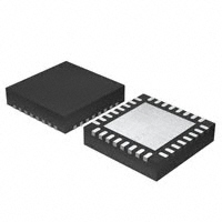
32-Pin 5y5 mm QFN Package
DESCRIPTION
The TLV320DAC26 is a high-performance audio DAC with
16/20/24/32-bit 97-dBA stereo playback.The audio output
drivers on the ’DAC26 are highly flexible, having
software-programmable low or high-power drive modes to
optimize system power dissipation. The outputs can be
configured to supply up to 330 mW into a bridge terminated
8-Ω load, can support stereo 16-Ω headphone amplifiers
in ac-coupled or capless output configurations, and can
supply a stereo line-level output
A programmable digital audio effects processor enables
bass, treble, midrange, or equalization playback
processing. The digital audio data format is programmable
to work with popular audio standard protocols (I2S, DSP,
Left/Right Justified) in master or slave mode, and also
includes an on-chip programmable PLL for flexible clock
generation capability. Highly configurable software power
control is provided, enabling stereo audio playback at 48
ksps at 11 mW with a 3.3-V analog supply level.
The ’DAC26 is available in a 32 lead QFN.
APPLICATIONS
D MP3 Players
D Digital Still Cameras
D Digital Video Camcorders
Please be aware that an important notice concerning availability, standard warranty, and use in critical applications of Texas Instruments
semiconductor products and disclaimers thereto appears at the end of this data sheet.
SPI is a trademark of Motorola.
I2S is a trademark of Phillips Electronics.
���� ���� ���� �������!��� �" #$��%�! �" �� &$'(�#�!��� )�!%*
��)$#!"
#������ !� "&%#���#�!���" &%� !+% !%��" �� �%,�" ��"!�$�%�!" "!��)��) -�����!.*
��)$#!��� &��#%""��/ )�%" ��! �%#%""���(. ��#($)% !%"!��/ �� �(( &����%!%�"*
Copyright 2004, Texas Instruments Incorporated
��������� �
www.ti.com
SLAS428− AUGUST 2004
This integrated circuit can be damaged by ESD. Texas Instruments recommends that all integrated circuits be handled with appropriate
precautions. Failure to observe proper handling and installation procedures can cause damage.
ESD damage can range from subtle performance degradation to complete device failure. Precision integrated circuits may be more susceptible to
damage because very small parametric changes could cause the device not to meet its published specifications.
PACKAGE/ORDERING INFORMATION
PRODUCT
PACKAGE
PACKAGE
DESIGNATOR
OPERATING
TEMPERATURE RANGE
TLV320DAC26
QFN-32
RHB
−40°C to 85°C
ORDERING NUMBER
TRANSPORT MEDIA,
QUANTITY
TLV320DAC26IRHB
Tubes, 74
TLV320DAC26IRHBR
Tape and Reel, 3000
PIN ASSIGNMENTS
QFN
DVDD
BCLK
NC
DIN
PWD
LRCK
RESET
HPR
(TOP VIEW)
32 31 30 29 28 27 26 25
DVSS
IOVDD
MCLK
SCLK
MISO
MOSI
SS
NC
1
24
2
23
22
3
4
5
21
20
DAC26
7
19
18
8
17
6
DRVDD
VGND
DRVSS
HPL
AVDD
NC
NC
NC
MICBIAS
MICIN
AUX
NC
NC
NC
AVSS
NC
9 10 11 12 13 14 15 16
Terminal Functions
QFN
PIN
2
NAME
DESCRIPTION
QFN
PIN
NAME
DESCRIPTION
1
DVSS
Digital core and IO ground
17
NC
No connect
2
IOVDD
IO supply
18
NC
No connect
3
MCLK
Master clock
19
NC
No connect
4
SCLK
SPI serial clock input
20
AVDD
5
MISO
SPI serial data output
21
HPL
6
MOSI
SPI serial data input
22
DRVSS
Speaker ground
7
SS
SPI slave select input
23
VGND
Virtual ground for audio output
8
NC
No connect
24
DRVDD
9
MICBIAS
Microphone bias voltage
25
HPR
10
MICIN
Microphone input
26
RESET
11
AUX
Auxiliary input
27
LRCK
Audio DAC word-clock
12
NC
No connect
28
PWD
Hardware powerdown
13
NC
No connect
29
DIN
Audio data input
14
NC
No connect
30
NC
No connect
15
AVSS
Analog ground
31
BCLK
Audio bit−clock
16
NC
No connect
32
DVDD
Digital core supply
Analog power supply
Left channel audio output
Speaker /PLL supply
Right channel audio output
Device reset
��������� �
www.ti.com
SLAS428− AUGUST 2004
ABSOLUTE MAXIMUM RATINGS
over operating free-air temperature range unless otherwise noted(1)(2)
UNITS
AVDD to AVSS
−0.3 V to 3.9 V
DRVDD to DRVSS
−0.3 V to 3.9 V
IOVDD to DVSS
−0.3 V to 3.9 V
DVDD to DVSS
−0.3 V to 2.5 V
AVDD to DRVDD
−0.1 V to 0.1 V
AVSS to DRVSS to DVSS
−0.1 V to 0.1 V
Analog inputs to AVSS
−0.3 V to AVDD + 0.3 V
Digital input voltage to DVSS
−0.3 V to IOVDD + 0.3 V
Operating temperature range
−40°C to 85°C
Storage temperature range
−65°C to 105°C
Junction temperature (TJ Max)
105°C
Power dissipation
QFN package
(TJ Max − TA)/θJA
123°C/W
θJA Thermal impedance
Soldering vapor phase (60 sec)
Lead temperature
215°C
Infrared (15 sec)
220°C
(1) Stresses beyond those listed under “absolute maximum ratings” may cause permanent damage to the device. These are stress ratings only, and
functional operation of the device at these or any other conditions beyond those indicated under “recommended operating conditions” is not
implied. Exposure to absolute-maximum-rated conditions for extended periods may affect device reliability.
(2) If the ’DAC26 is used to drive high power levels to an 8-Ω load for extended intervals at ambient temperatures above 70°C, multiple vias should be
used to electrically and thermally connect the thermal pad on the QFN package to an internal heat-dissipating ground plane on the user’s PCB.
ELECTRICAL CHARACTERISTICS
At +25°C, AVDD,DRVDD,IOVDD = 3.3 V, DVDD = 1.8 V, Int. Vref = 2.5 V, Fs (Audio) = 48 kHz, unless otherwise noted
PARAMETER
TEST CONDITIONS
MIN
TYP
MAX
UNITS
MICROPHONE INPUT
Input resistance
20
kΩ
Input capacitance
10
pF
D4 = 0 control register 05H/Page2
2.5
V
D4 = 1 control register 05H/Page2
2.0
V
4.7
mA
MICROPHONE BIAS
Voltage
Sourcing current
3
��������� �
www.ti.com
SLAS428− AUGUST 2004
ELECTRICAL CHARACTERISTICS
At +25°C, AVDD,DRVDD,IOVDD = 3.3 V, DVDD = 1.8 V, Int. Vref = 2.5 V, Fs (Audio) = 48 kHz, unless otherwise noted (continued)
PARAMETER
TEST CONDITIONS
MIN
TYP
MAX
UNITS
DAC INTERPOLATION FILTER
Pass band
20
0.45 Fs
±0.06
Pass band ripple
Transition band
Stop band
Hz
dB
0.45 Fs
0.5501 Fs
Hz
0.5501 Fs
7.455 Fs
Hz
Stop band attenuation
Filter group delay
De−emphasis error
65
dB
21/Fs
sec
±0.1
dB
1-kHz sine wave input, 48 ksps, output drivers
in low power mode, load = 10 kΩ, 10 pF
DAC LINE OUTPUT
Full scale output voltage (0 dB)
By design, D10−D9 = 00 in control register
06H/Page2 corresponding to 2-VPP output
swing
0.707
Vrms
Output common mode
By design, D10−D9 = 00 in control register
06H/Page2 corresponding to 2-VPP output
swing
1.35
V
SNR
Measured as idle channel noise, A-weighted
THD
0-dB FS input, 0-dB gain
PSRR
1 kHz, 100 mVpp on AVDD(2) VGND powered
down
DAC HEADPHONE OUTPUT
1-kHz sine wave input, 48 ksps, output drivers
in high power mode, load = 16 Ω, 10 pF
Full scale output voltage (0 dB)
By design, D10−D9 = 00 in control register
06H/Page2 corresponding to 2-VPP output
swing
SNR
Measured as idle channel noise, A-weighted
THD
−1 dB FS input, 0-dB gain
PSRR
1 kHz, 100 mVpp on AVDD(1) VGND powered
down
85
85
dB
56
dB
dBA
−55
54
dB
dB
121
dB
30
mW
−63.5
Digital volume control step size
Vrms
97
−91
D10−D9 = 00 in control register 06H/Page2
Digital volume control gain
dBA
0.707
Mute attenuation
Maximum output power
97
−95
0
dB
0.5
dB
80
dB
Channel separation
Between HPL and HPR
DAC SPEAKER OUTPUT
Output driver in high power mode,
load = 8 Ω,, connected between HPR and HPL
pins. D10−D9 = 10 in control register
06H/Page2 corresponding to 2.402-VPP output
swing
Output power
0 dB input to DAC
325
mW
SNR
Measured as idle channel noise, A-weighted
102
dBA
THD
−1 dB FS input, 0-dB gain
−86
dB
−6 dB FS input, 0-dB gain
−88
dB
(1) DAC PSRR measurement is calculated as:
ǒ
PSRR + 20 log 10
4
Ǔ
VSIG sup
V
HPRńL
��������� �
www.ti.com
SLAS428− AUGUST 2004
ELECTRICAL CHARACTERISTICS
At +25°C, AVDD,DRVDD,IOVDD = 3.3 V, DVDD = 1.8 V, Int. Vref = 2.5 V, Fs (Audio) = 48 kHz, unless otherwise noted (continued)
PARAMETER
TEST CONDITIONS
MIN
TYP
MAX
UNITS
VOLTAGE REFERENCE
Voltage range
VREF output programmed as 2.5 V
2.3
2.5
2.7
VREF output programmed as 1.25 V
1.15
1.25
1.35
Voltage range
External VREF. By design, not tested in
production.
Reference drift
Internal VREF = 1.25 V
Current drain
Extra current drawn when the internal
reference is turned on.
1.2
2.55
V
V
29
ppm/°C
650
µA
8.8
MHz
DIGITAL INPUT / OUTPUT(1)
Internal clock frequency
Logic family
CMOS
Logic level:
VIH
VIL
VOH
VOL
Capacitive load
IIH = +5 µA
IIL = +5 µA
0.7xIOVDD
IOH = 2 TTL loads
IOL = 2 TTL loads
0.8xIOVDD
V
−0.3
0.3xIOVDD
V
V
0.1xIOVDD
10
V
pF
POWER SUPPLY REQUIREMENTS
Power supply voltage
AVDD(2)
2.7
3.6
DRVDD(2)
2.7
3.6
V
IOVDD
1.1
3.6
V
1.95
V
DVDD
1.525
IAVDD
Stereo audio playback
IDRVDD
IDVDD
48 ksps, output drivers in low
power mode, VGND off, PLL
off
IAVDD
PLL
IDRVDD
IDVDD
0
mA
2.4
1.3
mA
0.9
IAVDD
IDRVDD
2.2
0.1
Additional power consumed
when PLL is enabled.
IDVDD
VGND
V
0.3
Additional power consumed
when VGND is powered.
0.9
mA
0
Hardware power down
All currents
2
µA
(1) Internal oscillator is designed to give nominally 8-MHz clock frequency. However, due to process variations, this frequency can vary from device
to device. All calculations for delays and wait times in the data sheet assume an 8-MHz oscillator clock.
(2) It is recommended that AVDD and DRVDD be set to the same voltage for the best performance. It is also recommended that these supplies be
separated on the user’s PCB.
5
��������� �
www.ti.com
SLAS428− AUGUST 2004
FUNCTIONAL BLOCK DIAGRAM
DRVDD DRVSS AVDD AVSS DVDD DVSS IOVDD
0 to -63.5 dB
(0.5 dB steps)
High Power
HPL
Programmable
PLL
DAC
Digital
Filters
DAC
Digital
Bass,
Midrange,
Treble,
EQ
Processing
MCLK
Low Power
High Power
HPR
Low Power
VGND
MICBIAS
MICIN
2.0 V / 2.5 V
+
−
AUX
Digital Audio
Serial
Interface
PWD
LRCK
BCLK
DIN
M
U
X
Control
Interface
SPI Serial
Interface and
Data
Processing
SS
SCLK
MOSI
MISO
RESET
OSC
6
��������� �
www.ti.com
SLAS428− AUGUST 2004
SPI TIMING DIAGRAM
SS
t
t
t en1
t en2
td
s ck
SCLK
t w(swk)
tf
tr
t w(swk)
tv
MISO
t h2
MSB OUT
t dis
BIT . . . 1
LSB OUT
ta
MOSI
t h1
t su
MSB OUT
BIT . . . 1
LSB OUT
TYPICAL TIMING REQUIREMENTS
All specifications at 25°C, DVDD = 1.8 V (1)
IOVDD = 1.1 V
PARAMETER
MIN
MAX
IOVDD = 3.3 V
MIN
MAX
UNITS
tw(sck)
ten1
SCLK pulse width
27
18
ns
Enable lead time
18
15
ns
ten2
td
Enable lag time
18
15
ns
Sequential transfer delay time
18
ta
tdis
Slave MISO access time
tsu
th1
MOSI data setup time
6
6
ns
MOSI data hold time
6
6
ns
th2
tv
MISO data hold time
4
Slave MISO disable time
MISO data valid time
tr
Rise time
tf
Fall time
(1) These parameters are based on characterization and are not tested in production.
15
18
18
ns
15
ns
15
ns
4
ns
22
13
ns
6
4
ns
6
4
ns
7
��������� �
www.ti.com
SLAS428− AUGUST 2004
AUDIO INTERFACE TIMING DIAGRAMS
LRCK/ADWS
td(WS)
BCLK
ts(DI)
th(DI)
DIN
Figure 1. I2S/LJF/RJF Timing in Master Mode
TYPICAL TIMING REQUIREMENTS (FIGURE 1)
All specifications at 25°C, DVDD = 1.8 V (1)
IOVDD = 1.1 V
PARAMETER
MIN
MAX
IOVDD = 3.3 V
MIN
td(WS)
ts(DI)
LRCK delay time
25
DIN setup time
6
6
th(DI)
tr
DIN hold time
6
6
Rise time
tf
Fall time
(1) These parameters are based on characterization and are not tested in production.
MAX
15
UNITS
ns
ns
ns
10
6
ns
10
6
ns
LRCK/ADWS
td(WS)
td(WS)
BCLK
th(DI)
ts(DI)
DIN
Figure 2. DSP Timing in Master Mode
TYPICAL TIMING REQUIREMENTS (FIGURE 2)
All specifications at 25°C, DVDD = 1.8 V(1)
IOVDD = 1.1 V
PARAMETER
MIN
MAX
IOVDD = 3.3 V
MIN
LRCK delay time
DIN setup time
6
6
ns
th(DI)
tr
DIN hold time
6
6
ns
Rise time
8
15
UNITS
td(WS)
ts(DI)
tf
Fall time
(1) These parameters are based on characterization and are not tested in production.
25
MAX
ns
10
6
ns
10
6
ns
��������� �
www.ti.com
SLAS428− AUGUST 2004
LRCK/ADWS
th(WS)
BCLK
tL(BCLK)
tS(WS)
tH(BCLK)
th(DI)
ts(DI)
tP(BCLK)
DIN
Figure 3. I2S/LJF/RJF Timing in Slave Mode
TYPICAL TIMING REQUIREMENTS (FIGURE 3)
All specifications at 25°C, DVDD = 1.8 V (1)
IOVDD = 1.1 V
PARAMETER
MIN
MAX
IOVDD = 3.3 V
MIN
MAX
UNITS
tH(BCLK)
tL(BCLK)
BCLK high period time
35
35
ns
BCLK low period time
35
35
ns
ts(WS)
th(WS)
LRCK setup time
6
6
ns
LRCK hold time
6
6
ns
ts(DI)
th(DI)
DIN setup time
6
6
ns
DIN hold time
6
tr
Rise time
tf
Fall time
(1) These parameters are based on characterization and are not tested in production.
6
ns
5
4
ns
5
4
ns
9
��������� �
www.ti.com
SLAS428− AUGUST 2004
LRCK/ADWS
tS(WS)
tH(BCLK)
th(WS)
th(WS)
tS(WS)
tL(BCLK)
BCLK
tP(BCLK)
th(DI)
DIN
Figure 4. DSP Timing in Slave Mode
TYPICAL TIMING REQUIREMENTS (FIGURE 4)
All specifications at 25°C, DVDD = 1.8 V (1)
IOVDD = 1.1 V
PARAMETER
MIN
MAX
IOVDD = 3.3 V
MIN
MAX
UNITS
tH(BCLK)
tL(BCLK)
BCLK high period
35
35
ns
BCLK low period
35
35
ns
ts(WS)
th(WS)
LRCK setup time
6
6
ns
LRCK hold time
6
6
ns
ts(DI)
th(DI)
DIN setup time
6
6
ns
DIN hold time
6
6
tr
Rise time
tf
Fall time
(1) These parameters are based on characterization and are not tested in production.
10
ns
5
4
ns
5
4
ns
��������� �
www.ti.com
SLAS428− AUGUST 2004
TYPICAL CHARACTERISTICS
0
−20
−40
dB
−60
−80
−100
−120
−140
−160
0
5000
10000
15000
20000
Hz
Figure 5. DAC FFT Plot (TA = 25°C, 48 ksps, 0 dB, 1 kHz Input, AVDD = 3.3 V, RL = 10 kΩ)
0
−10
−30
dB
−50
−70
−90
−110
−130
−150
0
5000
10000
Hz
15000
20000
Figure 6. DAC FFT Plot (TA = 25°C, 48 ksps, −1 dB, 1 kHz Input, AVDD = DRVDD = 3.3 V, DVDD = 1.8 V, RL
= 16 Ω)
THD − Total Harmonic Distortion − dB
−88
−90
−92
−94
5
15
25
35
Output Power − mW
Figure 7. High Power Output Driver THD vs Output Power
(TA =25°C, AVDD, DRVDD = 3.3 V, RL = 16 W)
11
��������� �
www.ti.com
SLAS428− AUGUST 2004
OVERVIEW
The TLV320DAC26 is a highly integrated stereo audio DAC for portable computing, communication, and entertainment
applications. The ’DAC26 has a register-based architecture where all functions are controlled through the registers and
onboard state machines.
The ’DAC26 consists of the following blocks (refer to the block diagram):
D
D
Audio DAC
Auxiliary Inputs for analog pass through functionality
Audio data is transferred between the host DSP/µP via a standard 4-wire interface and supports a variety of modes (i.e.,
I2S, DSP, etc).
Control of the ’DAC26 and its functions is accomplished by writing to different registers in the ’DAC26. A simple command
protocol is used to address the 16-bit registers. Registers control the operation of the audio DAC. The control and auxiliary
functions are accessed via a SPI bus.
A typical application of the ’DAC26 is shown in Figure 8.
I2S Interface
MCLK
Auxiliary Input
Audio
AUX
2.2 kW
MICBIAS
MICIN
PWD
Master Clock Input
ADC Word Select
DOUT
Serial Output to CPU/DSP
LRCK
DAC Word Select
DIN
BCLK
Serial Input From CPU/DSP
Serial Clock Input
HPR
SPI Interface
VGND
HPL
8W
Speaker
MISO
Serial Output to SPI Master
MOSI
Serial Input From SPI Master
SS
SPI Slave Select Input
SCLK
SPI Serial Clock Input
Figure 8. Typical Circuit Configuration
12
��������� �
www.ti.com
SLAS428− AUGUST 2004
OPERATION−AUDIO DAC
Audio Analog I/O
The ’DAC26 has one mono audio input (MICIN) typically used for microphone recording, and an auxiliary input (AUX) that
can be used as a second microphone or line input. The ’DAC26 has an analog pass through mode where by the input from
the Mic and AUX input can be routed to any one of the analog output drivers. The dual audio output drivers have
programmable power level and can be configured to drive up to 325 mW into an 8-Ω speaker, or to drive 16-Ω stereo
headphones at over 30-mW per channel, or to provide a stereo line-level output. The power level of the output drivers is
controlled using bit D12 in control register REG−05H/Page2. The ’DAC26 also has a virtual ground (VGND) output driver,
which can optionally be used to connect the return terminal of headphones, to eliminate the ac-coupling capacitors needed
at the headphone output. The VGND amplifier is controlled by bit D8 of REG−05H/Page2. A special circuit has also been
included in the ’DAC26 to insert a short keyclick sound into the stereo audio output, even when the audio DAC is powered
down. The keyclick sound is used to provide feedback to the user when a particular button is pressed or item is selected.
The specific sound of the keyclick can be adjusted by varying several register bits that control its frequency, duration, and
amplitude.
Audio Digital Interface
Digital audio data samples are transmitted between the ’DAC26 and the audio processor via the serial bus (BCLK, LRCK,
DIN) that can be configured to transfer digital data in four different formats: right justified, left justified, I2S, and DSP. The
four modes are MSB-first and operate with variable word length of 16, 20, 24, or 32 bits. The digital audio serial bus of the
’DAC26 can operate in master or slave mode, depending on its register settings. The word-select signal (LRCK) and bit
clock signal (BCLK) are configured as outputs when the bus is in master mode. They are configured as inputs when the
bus is in slave mode. The LRCK is representative of the audio DAC sampling rate and is synchronized with DIN.
D DAC SAMPLING RATE
The Audio Control 1 register (Register 00H, Page2) determines the sampling rates of the audio DAC, which is scaled
down from a reference rate (Fsref). When the audio DAC is powered up, it is configured by default as an I2S slave with
the DAC operating at Fsref.
D WORD SELECT SIGNALS
The word select signal (LRCK) indicates the channel being transmitted:
−
LRCK = 0: left channel for I2S mode
−
LRCK = 1: right channel for I2S mode
For other modes see the timing diagrams below.
Bitclock (BCLK) Signal
In addition to flexibility as master or slave mode, the BCLK can also be configured in two transfer modes—256−S and
Continuous Transfer Modes. These modes are set using bit D12/REG−06h/Page2.
D 256−S TRANSFER MODE
In the 256−S mode, the BCLK rate always equals 256 times the maximum of the LRCK frequencies. In
the 256−S mode, the DAC sampling rate equal to Fsref (as selected by bit D5−D0/REG−00h/Page2) and left−justified
mode is not supported.
D CONTINUOUS TRANSFER MODE
In the continuous transfer mode, the BCLK rate always equals two times the word length of the maximum of the LRCK
frequencies.
13
��������� �
www.ti.com
SLAS428− AUGUST 2004
D RIGHT-JUSTIFIED MODE
In right-justified mode, the LSB of the left channel is valid on the rising edge of the BCLK preceding the falling edge of
LRCK. Similarly, the LSB of the right channel is valid on the rising edge of the BCLK preceding the rising edge of LRCK.
1/fs
LRCK
BCLK
Left Channel
DIN/
0
n
n−1 n−2
Right Channel
2
MSB
1
0
n
n−1 n−2
2
1
0
LSB
Figure 9. Timing Diagram for Right-Justified Mode
D LEFT-JUSTIFIED MODE
In left−justified mode, the MSB of the right channel is valid on the rising edge of the BCLK, following the falling edge of
ADWS or LRCK. Similarly the MSB of the left channel is valid on the rising edge of the BCLK following the rising edge of
ADWS or LRCK.
1/fs
LRCK
BCLK
Left Channel
DIN
n
n−1 n−2
MSB
2
1
Right Channel
0
n
n−1 n−2
2
1
LSB
Figure 10. Timing Diagram for Left-Justified Mode
14
0
n
n−1
��������� �
www.ti.com
SLAS428− AUGUST 2004
D I2S MODE
In I2S mode, the MSB of the left channel is valid on the second rising edge of the BCLK after the falling edge of ADWS or
LRCK. Similarly the MSB of the right channel is valid on the second rising edge of the BCLK after the rising edge of
LRCK.
1/fs
LRCK
BCLK
1 clock before MSB
Left Channel
n
DIN
n−1 n−2
2
1
MSB
Right Channel
0
n
n−1 n−2
2
1
0
n
LSB
Figure 11. Timing Diagram for I2S Mode
D DSP MODE
In DSP mode, the falling edge of LRCK starts the data transfer with the left channel data first and immediately followed
by the right channel data. Each data bit is valid on the falling edge of BCLK.
1/fs
LRCK
BCLK
Left Channel
DIN/
1
0
n
n−1 n−2
LSB MSB
2
Right Channel
1
0
n
n−1 n−2
2
LSB MSB
1
0
n
n−1 n−2
LSB MSB
Figure 12. Timing Diagram for DSP Mode
15
��������� �
www.ti.com
SLAS428− AUGUST 2004
AUDIO DATA CONVERTERS
The ’DAC26 has a stereo audio DAC. The DAC can operate with a maximum sampling rate of 53 kHz and support all audio
standard rates of 8 kHz, 11.025 kHz, 12 kHz, 16 kHz, 22.05 kHz, 24 kHz, 32 kHz, 44.1 kHz, and 48 kHz. By utilizing the
flexible clock generation capability and internal programmable interpolation, a wide variety of sampling rates up to 53 kHz
can be obtained from many possible MCLK inputs.
When the DAC is operating, the ’DAC26 requires an applied audio MCLK input. The user should also set
bit D13/REG−06H/Page2 to indicate which Fsref rate is being used.
Typical audio DACs can suffer from poor out-of-band noise performance when operated at low sampling rates, such as
8 kHz or 11.025 kHz. The ’DAC26 includes programmable interpolation circuitry to provide improved audio performance
at such low sampling rates, by first upsampling low-rate data to a higher rate, filtering to reduce audible images, and then
passing the data to the internal DAC, which is actually operating at the Fsref rate. This programmable interpolation is
determined using bit D5−D3/REG−00H/Page2.
For example, if playback of 11.025-kHz data is required, the ’DAC26 can be configured such that Fsref = 44.1 kHz. Then
using bit D5−D3/REG−00H/Page2, the DAC sampling rate (Fs) can be set to Fsref/4, or Fs = 11.025 kHz. In operation, the
11.025-kHz digital input data is received by the ’DAC26, upsampled to 44.1 kHz, and filtered for images. It is then provided
to the audio DAC operating at 44.1 kHz for playback. In reality, the audio DAC further upsamples the 44.1 kHz data by a
ratio of 128x and performs extensive interpolation filtering and processing on this data before conversion to a stereo analog
output signal.
PLL
The ’DAC26 has an on-chip PLL to generate the needed internal DAC operational clocks from a wide variety of clocks
available in the system. The PLL supports an MCLK varying from 2 MHz to 50 MHz and is register programmable to enable
generation of required sampling rates with fine precision.
DAC sampling rates are given by
DAC_FS = Fsref/N1
where, Fsref must fall between 39 kHz and 53 kHz, and N1, N2 =1, 1.5, 2, 3, 4, 5, 5.5, 6 are register programmable.
The PLL can be enabled or disabled using register programming.
D
When PLL is disabled
Fsref + MCLK
128 Q
Q = 2, 3…17
−
D
In this mode, the MCLK can operate up to 50 MHz, and Fsref should fall within 39 kHz to 53 kHz.
When PLL is enabled
Fsref + MCLK
2048
K
P
P = 1, 2, 3, …, 8
K = J.D
J = 1, 2, 3, ….,64
D = 0, 1, 2, …, 9999
P, J, and D are register programmable, where J is an integer part of K before the decimal point, and D is a four-digit fractional
part of K after the decimal point, including lagging zeros.
Examples:
If K = 8.5, Then J = 8, D = 5000
If K = 7.12, Then J = 7, D = 1200
If K = 7.012, Then J = 7, D = 120
The PLL is programmed through Registers 1BH and 1CH of Page2.
16
��������� �
www.ti.com
SLAS428− AUGUST 2004
D
When PLL is enabled and D = 0, the following condition must be satisfied
2 MHz v MCLK v 20 MHz
P
80 MHz v MCLK
P
K v 110 MHz
4 v J v 55
D
When PLL is enabled and D ≠ 0, the following condition must be satisfied
10 MHz v MCLK v 20 MHz
P
80 MHz v MCLK
P
K v 110 MHz
4 v J v 11
Example 1:
For MCLK = 12 MHz and Fsref = 44.1 kHz
P = 1, K = 7.5264
⇒ J = 7, D = 5264
Example 2:
For MCLK = 12 MHz and Fsref = 48.0 kHz
P = 1, K = 8.192
⇒ J = 8, D = 1920
STEREO AUDIO DAC
Each channel of the stereo audio DAC consists of a digital audio processing block, a digital interpolation filter, digital
delta-sigma modulator, and an analog reconstruction filter. The DAC is designed to provide enhanced performance at low
sample rates through increased oversampling and image filtering, thereby keeping quantization noise generated within the
delta-sigma modulator and signal images strongly suppressed within the audio band to beyond 20 kHz. This is realized
by keeping the upsampled rate constant at 128 x Fsref and changing the oversampling ratio as the input sample rate is
changed. For Fsref of 48 kHz, the digital delta-sigma modulator always operates at a rate of 6.144 MHz. This ensures that
quantization noise generated within the delta-sigma modulator stays low within the frequency band below 20 kHz at all
sample rates. Similarly, for Fsref rate of 44.1 kHz, the digital delta-sigma modulator always operates at a rate of 5.6448
MHz.
Digital Audio Processing
The DAC channel consists of optional filters for de-emphasis and bass, treble, midrange level adjustment, or speaker
equalization. The de-emphasis function is only available for sample rates of 32 kHz, 44.1 kHz, and 48 kHz. The transfer
function consists of a pole with time constant of 50 µs and a zero with time constant of 15 µs. Frequency response plots
are given in the Audio DAC Filter Frequency Responses section of this data sheet. The de-emphasis filter can be enabled
or bypassed depending on bit D0 of register 05H/Page2.
The DAC digital effects processing block also includes a fourth order digital IIR filter with programmable coefficients (one
set per channel). The filter is implemented as cascade of two biquad sections with frequency response given by:
ǒ
Ǔǒ
N0 ) 2 N1 z *1 ) N2 z *2
32768 * 2 D1 z *1 * D2 z *2
Ǔ
N3 ) 2 N4 z *1 ) N5 z *2
32768 * 2 D4 z *1 * D5 z *2
The N and D coefficients are fully programmable, and the entire filter can be enabled or bypassed depending on bit D1 of
register 05H/Page2. The coefficients for this filter implement a variety of sound effects, with bass-boost or treble boost being
the most commonly used in portable audio applications. The default N and D coefficients in the part are given by:
N0 = N3 = 27619
N1 = N4 = −27034
N2 = N5 = 26461
D1 = D4 = 32131
D2 = D5 = −31506
17
��������� �
www.ti.com
SLAS428− AUGUST 2004
and implement a shelving filter with 0 dB gain from dc to approximately 150 Hz, at which point it rolls off to a 3-dB attenuation
for higher frequency signals, thus giving a 3-dB boost to signals below 150 Hz. The N and D coefficients are represented
by 16-bit twos complement numbers with values ranging from –32768 to +32767. Frequency response plots are given in
the Audio DAC Filter Frequency Responses section of this data sheet.
Interpolation Filter
The interpolation filter upsamples the output of the digital audio processing block by the required oversampling ratio. It
provides a linear phase output with a group delay of 21/Fs.
In addition, a digital interpolation filter provides enhanced image filtering and reduces signal images caused by the
upsampling process that are below 20 kHz. For example, upsampling an 8-kHz signal produces signal images at multiples
of 8 kHz (i.e., 8 kHz, 16 kHz, 24 kHz, etc). The images at 8 kHz and 16 kHz are below 20 kHz and still audible to the listener;
therefore, they must be filtered heavily to maintain good output quality. The interpolation filter is designed to maintain at
least 65-dB rejection of images that land below 7.455 Fs. In order to utilize the programmable interpolation capability, the
Fsref should be programmed to a higher rate (restricted to be in the range of 39 kHz to 53 kHz when the PLL is in use),
and the actual Fs is set using the dividers in bit D5−D3/REG−00H/Page2. For example, if Fs = 8 kHz is required, then Fsref
can be set to 48 kHz, and the DAC Fs set to Fsref/6. This ensures that all images of the 8-kHz data are sufficiently attenuated
well beyond the ~20-kHz audible frequency range.
Delta-Sigma DAC
The audio digital-to-analog converter incorporates a third order multibit delta-sigma modulator followed by an analog
reconstruction filter. The DAC provides high-resolution, low-noise performance, using oversampling and noise shaping
techniques. The analog reconstruction filter design consists of a 6 tap analog FIR filter followed by a continuous time RC
filter. The analog FIR operates at a rate of 128 x Fsref (6.144 MHz when Fsref = 48 kHz, 5.6448 MHz when Fsref = 44.1 kHz).
Note that the DAC analog performance may be degraded by excessive clock jitter on the MCLK input. Therefore, care must
be taken to keep jitter on this clock to a minimum.
DAC Digital Volume Control
The DAC has a digital volume control block, which implements programmable gain. The volume level can be varied from
0 dB to –63.5 dB in 0.5 dB steps. In addition, there is an independent mute bit for each channel. The volume level of both
channels can also be changed simultaneously by the master volume control. The gain is implemented with a soft-stepping
algorithm, which only changes the actual volume by one step per input sample, either up or down, until the desired volume
is reached. The rate of soft-stepping can be slowed to one step per two input samples through bit D1 of control register
04H/Page2.
Because of soft-stepping, the host does not know when the DAC has been actually muted. This may be important if the
host wishes to mute the DAC before making a significant change, such as changing sample rates. In order to help with this
situation, the ’DAC26 provides a flag back to the host via a read-only register bit (D2−D3 of control register 04H/Page2)
that alerts the host when the part has completed the soft-stepping and the actual volume has reached the desired volume
level. The soft-stepping feature can be disabled by programming D14=1 in register 1DH in Page02. If soft-stepping is
enabled, the MCLK signal to the device should not be changed until the DAC power-down flag is set. When this flag is set,
the internal soft-stepping process and power-down sequence is complete, and the MCLK can be stopped if desired.
18
��������� �
www.ti.com
SLAS428− AUGUST 2004
The ’DAC26 also includes functionality to detect when the user switches are on or off the de-emphasis or digital audio
processing functions, to first (1) soft-mute the DAC volume control, (2) change the operation of the digital effects
processing, and (3) soft-unmute the part. This avoids any possible pop/clicks in the audio output due to instantaneous
changes in the filtering. A similar algorithm is used when first powering up or down the DAC. The circuit begins operation
at power up with the volume control muted, then soft-steps it up to the desired volume level. At power down, the logic first
soft-steps the volume down to a mute level, then powers down the circuitry.
DAC Power Down
The DAC power-down flag ( D6 of REG05H/Page2) along with D10 of REG05H/Page2 denotes the power-down status
of the DAC according to Table 1.
Table 1. DAC Powerdown Status
[D10,D6]
POWERUP / DOWN STATE OF DAC
[0,0]
DAC is in stable power-up state
[0,1]
DAC is in the process of powering up. The length of this state is determined by PLL and output driver
power-up delays controlled by register programming.
[1,0]
DAC is in the process of powering down. The length of this state is determined by soft-stepping of volume
control block and DAC pop reduction sequencing controlled by register programming.
[1,1]
DAC is in a stable power-down state.
AUDIO OUTPUT DRIVERS
The ’DAC26 features audio output drivers which can be configured in either low power mode or high power mode depending
on the load and output power required. By default, at reset the output drivers are configured in low power mode. In this mode,
the output drivers can drive a full-scale line-level signal into loads of 10 kΩ minimum or drive moderate amplitude signals
into loads of 16 Ω minimum.
The output drivers can also be configured in high power mode by setting bit D12 of Reg05H/Page2 to 1. In this mode, each
output driver can deliver up to 30 mW per channel into a headphone speaker load of 16 Ω. The headphones can be
connected in a single-ended configuration using ac-coupling capacitors, or the capacitors can be removed and virtual
ground (VGND) powered for a capless output connection. The typical headphone jack configuration for these two modes
is shown in Figure 15. Note that the VGND amplifier must be powered if the capless configuration is used.
In the case of an ac-coupled output, the value of the capacitors is typically chosen based on the amount of low-frequency
cut that can be tolerated. The capacitor in series with the load impedance forms a high-pass filter with −3 dB cutoff frequency
of 1/(2πRC) in Hz, where R is the impedance of the headphones. Use of an overly small capacitor reduces low-frequency
components in the signal output and leads to low-quality audio. When driving 16-Ω headphones, capacitors of 220-µF (a
commonly used value) result in a high-pass filter cutoff frequency of 45 Hz, although reducing these capacitors to 50 µF
results in a cutoff frequency of 199 Hz, which is generally considered noticeable when playing music. The cutoff frequency
is reduced to half of the above values if 32-Ω headphones are used instead of 16 Ω.
The ’DAC26 programmable digital effects block can be used to help reduce the size of capacitors needed by implementing
a low frequency boost function to help compensate for the high-pass filter introduced by the ac-coupling capacitors. For
example, by using 50-µF capacitors and setting the ’DAC26 programmable filter coefficients as shown below, the frequency
response can be improved as shown in Figure 14.
Filter coefficients (use the same for both channels):
N0 = 32767, N1 = −32346, N2 = 31925, N3 = 32767, N4 = 0, N5 = 0
D0 = 32738, D1 = −32708 D4 = 0, D5 = 0
19
��������� �
www.ti.com
SLAS428− AUGUST 2004
0
−2
−4
Gain − dB
−6
−8
−10
−12
−14
−16
−18
−20
0
100 200 300 400 500 600 700 800 900 1 k
f − Frequency − Hz
Figure 13. Uncompensated Response For 16-W Load and 50-mF Decoupling Capacitor
0
Gain − dB
−5
−10
−15
−20
0
100 200 300 400 500 600 700 800 900 1 k
f − Frequency − Hz
Figure 14. Frequency Response For 16-W Load and 50-mF Decoupling Capacitor After Gain
Compensation Using a Suggested Set of Coefficients for Audio Effects Filter
Using the capless output configuration eliminates the need for these capacitors and removes the accompanying high-pass
filter entirely. However, this configuration does have one drawback – if the RETURN terminal of the headphone jack (which
is wired to the ’DAC26 VGND pin) is ever connected to a ground, that is shorted to the ’DAC26 ground pin, then the VGND
amplifier enters short-circuit protection, and the audio output does not function properly.
20
��������� �
www.ti.com
SLAS428− AUGUST 2004
’DAC26
’DAC26
HPR
HPR
HPL
HPL
Headphone Jack
VGND
VGND
Headphone Jack
Figure 15. Headphone Configurations, AC-Coupled (left) and Capless (right)
The audio output drivers in high power mode can also be configured to drive a mono differential signal into a speaker load
of 8-Ω minimum. The speaker load should be connected differentially between the HPR and HPL outputs. Several options
are possible for playback of DAC data in this case. If a stereo digital signal is available, this signal can be sent in normal
stereo fashion to the audio DAC. The programmable digital effects filters can then be used to invert one channel, so that
the signal applied across the speaker load is (LEFT + RIGHT), or effectively a mono-mix of the two channels. A simple
example of how to implement this inversion using the programmable filters is to set the coefficients as follows:
Left−channel coefficients:
N0=32767, N1=0, N2=0, N3=32767, N4=0, N5=0
D1=0, D2=0, D4=0, D5=0
Right−channel coefficients: N0=−32767, N1=0, N2=0, N3=32767, N4=0, N5=0
D1=0, D2=0, D4=0, D5=0
This provides no spectral shaping; it only inverts the right channel relative to the left channel, such that the signals at HPL
and HPR are (LEFT) and (−RIGHT), with the signal across the speaker then being LEFT+ RIGHT. In a general case when
spectral shaping is also desired, the inversion can be accomplished simply by setting N0, N1, and N2 coefficients of one
channel to the negative of the values set for the other channel. Note that the programmable filtering must be enabled by
setting bit D1/REG−05H/Page2 to 1.
To enable the output drivers to deliver higher output power, the DAC output swing should be set to its highest level by setting
bit D10−D9/REG−06H/Page2 to 11. It is possible to increase power even further by disabling the built-in short-circuit
protection by programming bit D8 of Reg1DH/Page2 to 1. In this case care must be taken so a short-circuit at the output
does not occur. Figure 16 shows a typical jack configuration using a capless output configuration. In this configuration, the
’DAC26 drives the loudspeaker whenever headphones are not inserted in the jack and drives the headphones whenever
it is inserted in the jack.
’DAC26
HPR
HPL
VGND
Headphone Jack
Loud Speaker
Figure 16. Speaker Connection
21
��������� �
www.ti.com
SLAS428− AUGUST 2004
0
THD − Total Harmonic Distortion − dB
−10
−20
2.402 VPP
−30
−40
−50
2 VPP
−60
−70
−80
−90
−100
0
50
100
150
200
250
300
350
PO − Output Power − mW
Figure 17. THD vs Output Power Delivered to an an 8-W Load (255C, AVDD = DRVDD = 3.3 V, DVDD = 1.8
V, DAC Output Swing Set to 2 V and 2.4V, and Short-Circuit Protection Disabled)
0
THD − Total Harmonic Distortion − dB
−10
−20
−30
−40
−50
−60
−70
−80
−90
−100
2.7
2.8
2.9
3
3.1
3.2
3.3
3.4
3.5
3.6
AVDD, DRVDD − V
Figure 18. THD vs AVDD, DRVDD Supply Voltage (255C When Driving a −1 dB, 1-kHz Sinewave From the
DAC Into an 8-W Load, with DAC Output Swing Set to 2.4 V, and Short-Circuit Protection Disabled)
The ’DAC26 incorporates a programmable short-circuit detection/protection function with different modes of operation.
During the insertion or removal of a headphone plug from the jack, the output pins of the drivers may be accidentally shorted,
causing the part to potentially draw a huge current, which may cause the power supply voltages to dip. Bits D8−D7 of
REG−1DH/Page2 control how the short-circuit detection/protection operates in the ’DAC26. One option is to fully disable
short-circuit protection, which also enables the audio output drivers to deliver more power to a low-impedance load (such
as an 8-Ω speaker). However, care must be taken to prevent any short-circuit from occurring while the part is in this mode.
A second programmable configuration enables current-limiting in the audio output drivers, so that excessive currents
cannot be provided if the outputs are shorted. It also enables the internal short-circuit detection function, which can detect
excess current being drawn from the drivers and set a short-circuit detect flag (Page2, REG−1DH, bit D6). This flag can
be read by the user to power down the drivers if desired. This flag is cleared only if the short-circuit condition is removed.
If the user does not monitor this flag and powers down the drivers when a short-circuit occurs, the current-limiting prevents
excessive currents from being drawn, but power dissipation is higher due to this limited current flowing through the short.
22
��������� �
www.ti.com
SLAS428− AUGUST 2004
In a third programmable configuration, the ’DAC26 can be programmed to monitor and automatically power down the audio
output drivers upon detection of a short-circuit condition (Page2, REG−1DH, bit D7), in addition to setting the short-circuit
flag in Page2, REG−1DH, bit−D6. When the device has detected a short and resulted in this condition, the short-circuit flag
is cleared when all the routings to the speaker driver are disabled (i.e., DAC, Analog Mixer, and Keyclick blocks are powered
down by user).
AUDIO OUTPUT DRIVER POWER-ON POP REDUCTION SCHEME
The ’DAC26 implements a pop reduction scheme to reduce audible artifacts during power up and power down of the audio
output drivers. This scheme can be controlled by programming bits D2 and D1 of REG1EH/Page2. By default, the driver
pop reduction scheme is enabled and can be disabled by programming bit D2 of Reg1EH/Page2 to 1. When this scheme
is enabled and the virtual ground connection is not used (VGND amplifier is powered down), the audio output driver slowly
charges up any external ac-coupling capacitors to reduce audible artifacts. Bit D1 of REG1EH/Page2 provides control of
the charging time for the ac-coupling capacitor as either 0.8 sec or 4 sec. When the virtual ground amplifier is powered up
and used, the external ac-coupling capacitor is eliminated, and the power up time becomes 1 ms. This scheme takes effect
whenever the audio output drivers are powered up due to enabling any of the DAC, the Analog Mixer, or the Keyclick
Generator.
Pop Reduction for DAC Routing
Whenever the audio DAC is powered on or off, a slight change in the output dc offset voltage may occur and can be heard
as a weak pop in the output. In order to reduce this artifact, the ’DAC26 implements a DAC pop reduction scheme, which
is programmable using bits D5−D2 in REG−1DH/Page2. Bit D5 enables the scheme, which implements a slow transition
between the starting dc level and the final dc level. For best results, program bits D4−D2 in REG1DH/Page2 to 100.
AUDIO MIXING
Analog Mixer
The analog mixer can be used to route the analog input selected (MICIN or AUX) through an analog volume control and
then mix it with the audio DAC output. The analog mixer feature is available only if single-ended MICIN or AUX is selected
as the input. This feature is available even if the DAC is powered down. The analog volume control in this path has a gain
range from 12 dB to –34.5 dB in 0.5-dB steps plus mute and includes soft-stepping logic. The internal oscillator is used
for soft-stepping whenever the DAC is powered down.
KEYCLICK
A special circuit has been included for inserting a square−wave signal into the analog output signal path based on register
control. This functionality is intended for generating keyclick sounds for user feedback. Register 04H/Page2 contains bits
that control the amplitude, frequency, and duration of the square-wave signal. The frequency of the signal can be varied
from 62.5 Hz to 8 kHz and its duration can be programmed from 2 periods to 32 periods. Whenever this register is written,
the square-wave is generated and coupled into the audio output, going to both audio outputs. The keyclick enable bit D15
of control register 04H/Page2 is reset after the duration of keyclick is played out. This capability is available even when
the DAC is powered down.
23
��������� �
www.ti.com
SLAS428− AUGUST 2004
SPI DIGITAL INTERFACE
All ’DAC26 control registers are programmed through a standard SPI bus. The SPI allows full-duplex, synchronous, serial
communication between a host processor (the master) and peripheral devices (slaves). The SPI master generates the
synchronizing clock and initiates transmissions. The SPI slave devices depend on a master to start and synchronize
transmissions.
A transmission begins when initiated by a master SPI. The byte from the master SPI begins shifting in on the slave SPIDIN
(MOSI) pin under the control of the master serial clock. As the byte shifts in on the SPIDIN pin, a byte shifts out on the
SPIDOUT (MISO) pin to the master shift register.
The idle state of the serial clock for the ’DAC26 is low, which corresponds to a clock polarity setting of 0 (typical
microprocessor SPI control bit CPOL = 0). The ’DAC26 interface is designed so that with a clock phase bit setting of 1
(typical microprocessor SPI control bit CPHA = 1), the master begins driving its MOSI pin and the slave begins driving its
SPIDOUT pin on the first serial clock edge. The SS pin can remain low between transmissions; however, the ’DAC26 only
interprets command words which are transmitted after the falling edge of SS.
Hardware Reset
The device requires a low-to-high pulse on RESET after power up for correct operation. A hardware reset pulse initializes
all the internal registers, counters, and logic.
Hardware Power Down
By default the PWD pin is configured as a hardware power-down (active low) signal. The device powers down all the internal
circuitry to save power. All the register contents are maintained. Some counters maintain their value.
24
��������� �
www.ti.com
SLAS428− AUGUST 2004
’DAC26 COMMUNICATION PROTOCOL
Register Programming
The ’DAC26 is entirely controlled by registers. An SPI master controlls the reading and writing of these registers by the
use of a 16-bit command, which is sent prior to the data for that register. The command is constructed as shown in Figure 19.
The command word begins with a R/W bit, which specifies the direction of data flow on the SPI serial bus. The following
four bits specify the page of memory this command is directed to, as shown in Table 2. The next six bits specify the register
address on that page of memory to which the data is directed. The last five bits are reserved for future use and should be
written only with zeros.
Table 2. Page Addressing
PG3
PG2
PG1
PG0
0
0
0
0
PAGE ADDRESSED
0
0
0
0
1
1
0
0
1
0
2
0
0
1
1
Reserved
0
1
0
0
Reserved
0
1
0
1
Reserved
0
1
1
0
Reserved
0
1
1
1
Reserved
1
0
0
0
Reserved
1
0
0
1
Reserved
1
0
1
0
Reserved
1
0
1
1
Reserved
1
1
0
0
Reserved
1
1
0
1
Reserved
1
1
1
0
Reserved
1
1
1
1
Reserved
To read all the first page of memory, for example, the host processor must send the command 0x8000 to the ’DAC26 – this
specifies a read operation beginning at page 0, address 0. The processor can then start clocking data out of the ’DAC26.
The ’DAC26 automatically increments its address pointer to the end of the page; if the host processor continues clocking
data out past the end of a page, the ’DAC26 sends back the value 0xFFFF.
Likewise, writing to page 1 of memory consists of the processor writing the command 0x0800, which specifies a write
operation, with PG0 set to 1, and all the ADDR bits set to 0. This results in the address pointer pointing at the first location
in memory on Page 1. See the section on the ’DAC26 memory map for details of register locations
BIT 15
MSB
BIT 14
BIT 13
BIT 12
BIT 11
BIT 10
BIT 9
BIT 8
BIT 7
BIT 6
BIT 5
BIT 4
BIT 3
BIT 2
BIT 1
BIT 0
LSB
R/W*
PG3
PG2
PG1
PG0
ADDR5
ADDR4
ADDR3
ADDR2
ADDR1
ADDR0
0
0
0
0
0
Figure 19. ’DAC26 Command Word
25
��������� �
www.ti.com
SLAS428− AUGUST 2004
SS
SCLK
MOSI
COMMAND WORD
DATA
DATA
Figure 20. Write Operation for ’DAC26 SPI Interface
SS
SCLK
MOSI
MISO
COMMAND WORD
DATA
Figure 21. Read Operation for ’DAC26 SPI Interface
26
DATA
��������� �
www.ti.com
SLAS428− AUGUST 2004
’DAC26 MEMORY MAP
The ’DAC26 has several 16-bit registers which allow control of the device as well as providing a location for results from
the ’DAC26 to be stored until read by the host microprocessor. These registers are separated into three pages of memory
in the ’DAC26: a data page (Page 0) and control pages (Page 1 and Page 2). The memory map is shown in Table 3.
Table 3. Memory Map
Page 0: Reserved
ADDR
Page 1: Auxiliary Control Registers
REGISTER
ADDR
REGISTER
Page 2: Audio Control Registers
ADDR
REGISTER
00
Reserved
00
Reserved
00
Audio Control 1
01
Reserved
01
Reserved
01
Reserved
02
Reserved
02
Reserved
02
DAC Gain
03
Reserved
03
Reserved
03
Analog Sidetone
04
Reserved
04
Reset
04
Audio Control 2
05
Reserved
05
Reserved
05
DAC Power Control
06
Reserved
06
Reserved
06
Audio Control 3
07
Reserved
07
Reserved
07
Digital Audio Effects Filter Coefficients
08
Reserved
08
Reserved
08
Digital Audio Effects Filter Coefficients
09
Reserved
09
Reserved
09
Digital Audio Effects Filter Coefficients
0A
Reserved
0A
Reserved
0A
Digital Audio Effects Filter Coefficients
0B
Reserved
0B
Reserved
0B
Digital Audio Effects Filter Coefficients
0C
Reserved
0C
Reserved
0C
Digital Audio Effects Filter Coefficients
0D
Reserved
0D
Reserved
0D
Digital Audio Effects Filter Coefficients
0E
Reserved
0E
Reserved
0E
Digital Audio Effects Filter Coefficients
0F
Reserved
0F
Reserved
0F
Digital Audio Effects Filter Coefficients
10
Reserved
10
Reserved
10
Digital Audio Effects Filter Coefficients
11
Reserved
11
Reserved
11
Digital Audio Effects Filter Coefficients
12
Reserved
12
Reserved
12
Digital Audio Effects Filter Coefficients
13
Reserved
13
Reserved
13
Digital Audio Effects Filter Coefficients
14
Reserved
14
Reserved
14
Digital Audio Effects Filter Coefficients
15
Reserved
15
Reserved
15
Digital Audio Effects Filter Coefficients
16
Reserved
16
Reserved
16
Digital Audio Effects Filter Coefficients
17
Reserved
17
Reserved
17
Digital Audio Effects Filter Coefficients
18
Reserved
18
Reserved
18
Digital Audio Effects Filter Coefficients
19
Reserved
19
Reserved
19
Digital Audio Effects Filter Coefficients
1A
Reserved
1A
Reserved
1A
Digital Audio Effects Filter Coefficients
1B
Reserved
1B
Reserved
1B
PLL Programmability
1C
Reserved
1C
Reserved
1C
PLL Programmability
1D
Reserved
1D
Reserved
1D
Audio Control 4
1E
Reserved
1E
Reserved
1E
Audio Control 5
1F
Reserved
1F
Reserved
1F
Reserved
27
��������� �
www.ti.com
SLAS428− AUGUST 2004
’DAC26 CONTROL REGISTERS
This section describes each of the registers shown in the memory map of Table 3. The registers are grouped according
to the function they control. In the ’DAC26, bits in control registers can refer to slightly different functions depending on
whether you are reading the register or writing to it.
’DAC26 Data Registers (Page 0)
The data registers in Page 0 are reserved.
PAGE 1 CONTROL REGISTER MAP
REGISTER 00H: Reserved
BIT
NAME
READ/
WRITE
RESET
VALUE
D15−D0
Reserved
R
FFFFH
FUNCTION
Reserved
REGISTER 01H: Reserved
BIT
NAME
READ/
WRITE
RESET
VALUE
D15−D0
Reserved
R
FFFFH
FUNCTION
Reserved
REGISTER 02H: Reserved
BIT
NAME
READ/
WRITE
RESET
VALUE
D15−D0
Reserved
R
FFFFH
FUNCTION
Reserved
REGISTER 03H: Reference Control
Register 03H is reserved.
REGISTER 04H: Reset Control
BIT
NAME
READ/
WRITE
RESET
VALUE
D15−D0
RSALL
R/W
FFFFH
28
FUNCTION
Reset All. Writing the code 0xBB00, as shown below, to this register causes the ’DAC26 to reset all
its registers to their default, power−up values.
1011101100000000 => Reset all registers
Others
=> Do not write other sequences to this register.
��������� �
www.ti.com
SLAS428− AUGUST 2004
PAGE 2 CONTROL REGISTER MAP
REGISTER 00H: Audio Control 1
BIT
NAME
READ/
WRITE
RESET
VALUE
D15−D14
FUNCTION
R/W
00
Reserved
D13−D12
AIN
R/W
00
Analog Input Mux
00 => Analog Input = Single-ended input MIC
01 => Analog Input = Single-ended input AUX
10 => Analog Input = Differential input MICIN and AUX
11 => Analog Input = Differential input MICIN and AUX
D11−D10
WLEN
R/W
00
DAC Word Length
00 => Word length = 16 bit
01 => Word length = 20 bit
10 => Word length = 24 bit
11 => Word length = 32 bit
D9−D8
DATFM
R/W
00
Digital Data Format
00 => I2S mode
01 => DSP mode
10 => Right justified
11 => Left justified
Note: Right justified mode is NOT valid only when the DAC sampling ratio is Fsref/11.5 or
Fsref/5.5
D7−D6
Reserved
R/W
00
Reserved
Note: Only write a 0 to this bit
D5−D3
DACFS
R/W
000
DAC Sampling Rate
000 => DAC FS = Fsref/1
001 => DAC FS = Fsref/(1.5)
010 => DAC FS = Fsref/2
011 => DAC FS = Fsref/3
100 => DAC FS = Fsref/4
101 => DAC FS = Fsref/5
110 => DAC FS = Fsref/(5.5)
111 => DAC FS = Fsref/6
Note: Fsref can be set between 39 kHz and 53 kHz
D2−D0
Reserved
R/W
000
Reserved
REGISTER 01H: Reserved
BIT
NAME
D15−D0
READ/
WRITE
RESET
VALUE
R
FFFFH
FUNCTION
Reserved
REGISTER 02H: DAC Gain Control
BIT
NAME
READ/
WRITE
RESET
VALUE
D15
DALMU
R/W
1
D14−D8
DALVL
R/W
1111111
FUNCTION
DAC Left Channel Muted
1 => DAC left channel muted
0 => DAC left channel not muted
DAC Left Channel Volume Control
0000000 => DAC left channel volume control = 0 dB
0000001 => DAC left channel volume control = −0.5 dB
0000010 => DAC left channel volume control = −1.0 dB
−−−−−
1111110 => DAC left channel volume control = −63.0 dB
1111111 => DAC left channel volume control = −63.5 dB
29
��������� �
www.ti.com
SLAS428− AUGUST 2004
REGISTER 02H: DAC Gain Control (continued)
BIT
NAME
READ/
WRITE
RESET
VALUE
D7
DARMU
R/W
1
D6−D0
DARVL
R/W
1111111
FUNCTION
DAC Right Channel Muted
1 => DAC right channel muted
0 => DAC right channel not muted
DAC Right Channel Volume Control
0000000 => DAC right channel volume control = 0 dB
0000001 => DAC right channel volume control = −0.5 dB
0000010 => DAC right channel volume control = −1.0 dB
−−−−−
1111110 => DAC right channel volume control = −63.0 dB
1111111 => DAC right channel volume control = −63.5 dB
REGISTER 03H: Analog Sidetone Control
BIT
NAME
READ/
WRITE
RESET
VALUE
D15
ASTMU
R/W
1
D14−D8
ASTG
R/W
1000101
FUNCTION
Analog Sidetone Mute Control
1 => Analog sidetone muted
0 => Analog sidetone not muted
Analog Sidetone Gain Setting
0000000 => Analog sidetone gain setting = −34.5 dB
0000001 => Analog sidetone gain setting = −34 dB
0000010 => Analog sidetone gain setting = −33.5 dB
−−−−−
1000101 => Analog sidetone gain setting = 0 dB
1000110 => Analog sidetone gain setting = 0.5 dB
−−−−−
1011100 => Analog sidetone gain setting = 11.5 dB
1011101 => Analog sidetone gain setting = 12 dB
1011110 => Analog sidetone gain setting = 12 dB
1011111 => Analog sidetone gain setting = 12 dB
−−−−−
11xxxxx => Analog sidetone gain setting = 12 dB
D7−D1
Reserved
R/W
1
Reserved
Note: Only write a 1 to this bit
D0
ASTGF
R
0
Analog Sidetone PGA Flag ( Read Only )
0 => Gain applied /= PGA register setting
1 => PGA applied = PGA register setting.
Note: Analog sidetone gain is implemented at zero crossings of the signal.
30
��������� �
www.ti.com
SLAS428− AUGUST 2004
REGISTER 04H: Audio Control 2
BIT
NAME
READ/
WRITE
RESET
VALUE
D15
KCLEN
R/W
0
D14−D12
KCLAC
R/W
100
FUNCTION
Keyclick Enable
0 => Keyclick disabled
1 => Keyclick enabled
Note: This bit is automatically cleared after giving out the keyclick signal length equal to the
programmed value.
Keyclick Amplitude Control
000 => Lowest amplitude
100 => Medium amplitude
111 => Highest amplitude
D11
Reserved
R/W
0
Reserved
Note: Only write a 0 to this bit
D10−D8
KCLFRQ
R/W
100
Keyclick Frequency
000 => 62.5 Hz
001 => 125 Hz
010 => 250 Hz
011 => 500 Hz
100 => 1 kHz
101 => 2 kHz
110 => 4 kHz
111 => 8 kHz
D7−D4
KCLLN
R/W
0001
Keyclick Length
0000 => 2 periods key click
0001 => 4 periods key click
0010 => 6 periods key click
−−−−−
1110 => 30 periods key click
1111 => 32 periods key click
D3
DLGAF
R
0
DAC Left Channel PGA Flag ( Read Only )
0 => Gain applied /= PGA register setting
1 => Gain applied = PGA register setting
Note: This flag indicates when the soft-stepping for DAC left channel is completed
D2
DRGAF
R
0
DAC Right Channel PGA Flag ( Read Only )
0 => Gain applied /= PGA register setting
1 => Gain applied = PGA register setting
Note: This flag indicates when the soft-stepping for DAC right channel is completed
D1
DASTC
R/W
0
DAC Channel PGA Soft-Stepping Control
0 => 0.5dB change every LRCK
1 => 0.5dB change every 2 LRCK
D0
Reserved
R/W
0
Reserved
Note: Only write a 0 to this bit
31
��������� �
www.ti.com
SLAS428− AUGUST 2004
REGISTER 05H: DAC Power Control
BIT
NAME
READ/
WRITE
RESET
VALUE
D15
PWDNC
R/W
1
DAC Power-Down Control
0 => DAC powered up
1 => DAC powered down
D14
Reserved
R/W
0
Reserved (During read the value of this bit is 0. Write only 0 into this location.)
Note: Only set this bit to the reset value 0 or 1
D13
ASTPWD
R/W
1
Analog Sidetone Power-down Control
0 => Analog sidetone powered up
1 => Analog sidetone powered down
D12
DAODRC
R/W
0
Audio Output Driver Control
0 => Output driver in low power mode
1 => Output driver in high power mode
D11
ASTPWF
R
1
Analog Sidetone Power-Down Flag
0 => Analog sidetone powered down is not complete.
1 => Analog sidetone powered down is complete.
D10
DAPWDN
R/W
1
DAC Power-Down Control
0 => Power up the DAC
1 => Power down the DAC
D9
Reserved
R/W
1
Reserved
Note: Only set this bit to the reset value 0 or 1
D8
VGPWDN
R/W
1
Driver Virtual Ground Power Down
0 => Power up the VGND amp
1 => Power down the VGND amp
D7
Reserved
R/W
1
Reserved
Note: Only set this bit to the reset value 0 or 1
D6
DAPWDF
R
1
DAC Power-Down Flag (See DAC Power down section of this data sheet)
0 => DAC power down is not complete.
1 => DAC power down is complete.
D5
Reserved
R/W
0
Reserved
Note: Only set this bit to the reset value 0 or 1
D4
VBIAS
R/W
0
VBIAS Voltage
0 => VBIAS output = 2.5 V
1 => VBIAS output = 2.0 V
D3−D2
Reserved
R/W
0
Reserved
Note: Only set this bit to the reset value 0 or 1
D1
EFFCTL
R/W
0
Digital Audio Effects Filter Control
0 => Disable digital audio effects filter
1 => Enable digital audio effects filter
D0
DEEMPF
R/W
0
De−Emphasis Filter Enable
0 => Disable de-emphasis filter
1 => Enable de-emphasis filter
32
FUNCTION
��������� �
www.ti.com
SLAS428− AUGUST 2004
REGISTER 06H: Audio Control 3
BIT
NAME
READ/
WRITE
RESET
VALUE
D15−D14
DMSVOL
R/W
00
DAC Channel Master Volume Control
00 => Left channel and right channel have independent volume controls
01 => Left channel volume control is the programmed value of the right channel volume control.
10 => Right channel volume control is the programmed value of the left channel volume control.
11 => same as 00
D13
REFFS
R/W
0
Reference Sampling Rate. This setting controls the coefficients in the de-emphasis filter. If an
Fsref above 48 kHz is being used, then it is recommended to set this to the 48-kHz setting,
otherwise either setting can be used.
0 => Fsref = 48.0 kHz
1 => Fsref = 44.1 kHz
D12
DAXFM
R/W
0
Master Transfer Mode
0 => Continuous data transfer mode
1 => 256−s data transfer mode
D11
SLVMS
R/W
0
DAC Master Slave Control
0 => ’DAC26 is slave
1 => ’DAC26 is master
D10−D9
DAPK2PK
R/W
00
DAC Max Output Signal Swing and Common Mode Voltage
00 => DAC max output signal swing = 2.0 V, VCM = 1.35 V
01 => DAC max output signal swing = 2.192 V (only recommended for analog supply of 3.0 V
and digital supply of 1.65 V and above), VCM = 1.48 V
10 => DAC max output signal swing = 2.402 V (only recommended for analog supply of 3.3 V
and digital supply of 1.8 V and above), VCM = 1.62 V
11 => DAC max output signal swing = 2.633 V (only recommended for analog supply of 3.6 V
and digital supply of 1.95 V), VCM = 1.78 V
D8
Reserved
R/W
0
Reserved
Note: Always write the reset value to this bit
D7
DALOVF
R
0
DAC Left Channel Overflow Flag ( Read Only )
0 => DAC left channel data is within saturation limits.
1 => DAC left channel data has exceeded saturation limits.
Note : This flag is reset only on register read.
D6
DAROVF
R
0
DAC Right Channel Overflow Flag ( Read Only )
0 => DAC right channel data is within saturation limits.
1 => DAC right channel data has exceeded saturation limits.
Note : This flag is reset only on register read.
D5−D0
Reserved
R/W
0
Reserved
Note: Always write the reset value to this bit
FUNCTION
33
��������� �
www.ti.com
SLAS428− AUGUST 2004
REGISTER 07H: Digital Audio Effects Filter Coefficients
BIT
NAME
READ/
WRITE
RESET VALUE
(IN DECIMAL)
D15−D0
L_N0
R/W
27619
FUNCTION
Left channel digital audio effects filter coefficient N0
REGISTER 08H: Digital Audio Effects Filter Coefficients
BIT
NAME
READ/
WRITE
RESET VALUE
(IN DECIMAL)
D15−D0
L_N1
R/W
−27034
FUNCTION
Left channel digital audio effects filter coefficient N1
REGISTER 09H: Digital Audio Effects Filter Coefficients
BIT
NAME
READ/
WRITE
RESET VALUE
(IN DECIMAL)
D15−D0
L_N2
R/W
26461
FUNCTION
Left channel digital audio effects filter coefficient N2
REGISTER 0AH: Digital Audio Effects Filter Coefficients
BIT
NAME
READ/
WRITE
RESET VALUE
(IN DECIMAL)
D15−D0
L_N3
R/W
27619
FUNCTION
Left channel digital audio effects filter coefficient N3
REGISTER 0BH: Digital Audio Effects Filter Coefficients
BIT
NAME
READ/
WRITE
RESET VALUE
(IN DECIMAL)
D15−D0
L_N4
R/W
−27034
FUNCTION
Left channel digital audio effects filter coefficient N4
REGISTER 0CH: Digital Audio Effects Filter Coefficients
BIT
NAME
READ/
WRITE
RESET VALUE
(IN DECIMAL)
D15−D0
L_N5
R/W
26461
FUNCTION
Left channel digital audio effects filter coefficient N5
REGISTER 0DH: Digital Audio Effects Filter Coefficients
BIT
NAME
READ/
WRITE
RESET VALUE
(IN DECIMAL)
D15−D0
L_D1
R/W
32131
FUNCTION
Left channel digital audio effects filter coefficient D1
REGISTER 0EH: Digital Audio Effects Filter Coefficients
BIT
NAME
READ/
WRITE
RESET VALUE
(IN DECIMAL)
D15−D0
L_D2
R/W
−31506
FUNCTION
Left channel digital audio effects filter coefficient D2
REGISTER 0FH: Digital Audio Effects Filter Coefficients
BIT
NAME
READ/
WRITE
RESET VALUE
(IN DECIMAL)
D15−D0
L_D4
R/W
32131
FUNCTION
Left channel digital audio effects filter coefficient D4
REGISTER 10H: Digital Audio Effects Filter Coefficients
BIT
NAME
READ/
WRITE
RESET VALUE
(IN DECIMAL)
D15−D0
L_D5
R/W
−31506
FUNCTION
Left channel digital audio effects filter coefficient D5
REGISTER 11H: Digital Audio Effects Filter Coefficients
BIT
NAME
READ/
WRITE
RESET VALUE
(IN DECIMAL)
D15−D0
R_N0
R/W
27619
FUNCTION
Right channel digital audio effects filter coefficient N0
REGISTER 12H: Digital Audio Effects Filter Coefficients
BIT
NAME
READ/
WRITE
RESET VALUE
(IN DECIMAL)
D15−D0
R_N1
R/W
−27034
34
FUNCTION
Right channel digital audio effects filter coefficient N1
��������� �
www.ti.com
SLAS428− AUGUST 2004
REGISTER 13H: Digital Audio Effects Filter Coefficients
BIT
NAME
READ/
WRITE
RESET VALUE
(IN DECIMAL)
D15−D0
R_N2
R/W
26461
FUNCTION
Right channel digital audio effects filter coefficient N2
REGISTER 14H: Digital Audio Effects Filter Coefficients
BIT
NAME
READ/
WRITE
RESET VALUE
(IN DECIMAL)
D15−D0
R_N3
R/W
27619
FUNCTION
Right channel digital audio effects filter coefficient N3
REGISTER 15H: Digital Audio Effects Filter Coefficients
BIT
NAME
READ/
WRITE
RESET VALUE
(IN DECIMAL)
D15−D0
R_N4
R/W
−27034
FUNCTION
Right channel digital audio effects filter coefficient N4
REGISTER 16H: Digital Audio Effects Filter Coefficients
BIT
NAME
READ/
WRITE
RESET VALUE
(IN DECIMAL)
D15−D0
R_N5
R/W
26461
FUNCTION
Right channel digital audio effects filter coefficient N5
REGISTER 17H: Digital Audio Effects Filter Coefficients
BIT
NAME
READ/
WRITE
RESET VALUE
(IN DECIMAL)
D15−D0
R_D1
R/W
32131
FUNCTION
Right channel digital audio effects filter coefficient D1
REGISTER 18H: Digital Audio Effects Filter Coefficients
BIT
NAME
READ/
WRITE
RESET VALUE
(IN DECIMAL)
D15−D0
R_D2
R/W
−31506
FUNCTION
Right channel digital audio effects filter coefficient D2
REGISTER 19H: Digital Audio Effects Filter Coefficients
BIT
NAME
READ/
WRITE
RESET VALUE
(IN DECIMAL)
D15−D0
R_D4
R/W
32131
FUNCTION
Right channel digital audio effects filter coefficient D4
REGISTER 1AH: Digital Audio Effects Filter Coefficients
BIT
NAME
READ/
WRITE
RESET VALUE
(IN DECIMAL)
D15−D0
R_D5
R/W
−31506
FUNCTION
Right channel digital audio effects filter coefficient D5
35
��������� �
www.ti.com
SLAS428− AUGUST 2004
REGISTER 1BH: PLL Programmability
BIT
NAME
READ/
WRITE
RESET VALUE
D15
PLLSEL
R/W
0
D14−D11
QVAL
R/W
0010
FUNCTION
PLL Enable
0 => Disable PLL
1 => Enable PLL
Q value. Valid only if PLL is disabled.
0000 => 16
0001 => 17
0010 => 2
0011 => 3
−−−−−
1100 => 12
1101 => 13
1110 => 14
1111 => 15
D10−D8
PVAL
R/W
000
P value. Valid when PLL is enabled
000 => 8
001 => 1
010 => 2
011 => 3
100 => 4
101 => 5
110 => 6
111 => 7
D7−D2
JVAL
R/W
000001
J value. Valid only if PLL is enabled.
000000 => Not valid
000001 => 1
000010 => 2
−−−−−
111110 => 62
111111 => 63
D1−D0
Reserved
R
00
Reserved (write only 00)
REGISTER 1CH: PLL Programmability
BIT
NAME
READ/
WRITE
RESET VALUE
D15−D2
DVAL
R/W
0 (in decimal)
D1−D0
Reserved
R
00
36
FUNCTION
D value. Used when PLL is enabled.
D value is valid from 0000 to 9999 in decimal.
Programmed value greater than 9999 is treated as 9999.
00000000000000 => 0 decimal
00000000000001 => 1 decimal
Reserved (write only 00)
��������� �
www.ti.com
SLAS428− AUGUST 2004
REGISTER 1DH: Audio Control 4
BIT
NAME
D15
READ/
WRITE
RESET
VALUE
R/W
0
Reserved
FUNCTION
D14
DASTPD
R/W
0
DAC PGA Soft-Stepping Control
0 => Soft-stepping enabled
1 => Soft-stepping disabled
D13
ASSTPD
R/W
0
Analog Sidetone Soft-Stepping Control
0 => Soft-stepping enabled
1 => Soft-stepping disabled
D12−D9
Reserved
R/W
0
Reserved
Note: Only write a 0 to this bit
D8
SHCKT_DIS
R/W
0
Disable Short Circuit Detection
0 => Short circuit detection enabled
1 => Short circuit detection disabled
D7
SHCKT_PD
R/W
0
Power Down Drivers if Short Circuit Detected
0 => No auto power down of drivers on short circuit.
1 => Auto power down drivers on short circuit.
D6
SHCKT_FLAG
R
0
Short Circuit Detected Flag
0 => Short circuit not detected
1 => Short circuit detected
D5
DAC_POP_RED
R
0
DAC POP Reduction Enable
0 => Disable POP reduction
1 => Enable POP reduction
D4
DAC_POP_RED_
SET1
R/W
0
DAC POP Reduction Setting 1
0 => Fast setting
1 => Slow setting
D3−D2
DAC_POP_RED_
SET2
R/W
00
DAC POP Reduction Setting 2
00 => Long setting
11 => Short setting
D1−D0
Reserved
R
XX
Reserved
REGISTER 1EH: Audio Control 5
BIT
NAME
READ/
WRITE
RESET
VALUE
D15−D3
Reserved
R/W
0
Reserved
Note: Only write a 0 to this bit
D2
DRV_POP_DIS
R/W
0
Audio Output Driver POP Reduction Enable
0 => Enabled
1 => Disabled
D1
DRV_POP_LEN
R/W
0
Audio Output Driver POP Reduction Duration
0 => Output driver ramps to final voltage in approximately 0.8 sec, if VGND is
powered down (1 msec otherwise).
1 => Output driver ramps to final voltage in approximately 4 sec, if VGND is powered
down (1 msec otherwise).
D0
Reserved
R
0
Reserved. Always write a 0 to this bit.
FUNCTION
37
��������� �
www.ti.com
SLAS428− AUGUST 2004
LAYOUT
The following layout suggestions should provide optimum performance from the ’DAC26. However, many portable
applications have conflicting requirements concerning power, cost, size, and weight. In general, most portable devices
have fairly clean power and grounds because most of the internal components are very low power. This situation means
less bypassing for the converter power and less concern regarding grounding. Still, each situation is unique and the
following suggestions should be reviewed carefully.
For optimum performance, care must be taken with the physical layout of the ’DAC26 circuitry. Power to the ’DAC26 must
be clean and well bypassed. A 0.1-µF ceramic bypass capacitor must be placed as close to the device as possible. A 1-µF
to 10-µF capacitor may also be needed if the impedance between the ’DAC26 supply pins and the system power supply
is high.
The ground pins must be connected to a clean ground point. In many cases, this is the analog ground. Avoid connections
which are too near the grounding point of a microcontroller or digital signal processor. If needed, run a ground trace directly
from the converter to the power supply entry or battery connection point. The ideal layout includes an analog ground plane
dedicated to the converter and associated analog circuitry.
38
��������� �
www.ti.com
SLAS428− AUGUST 2004
DAC CHANNEL DIGITAL FILTER
DAC Channel Digital Filter Frequency Response
Frequency Response of Full DAC Channel Digital Filterat Fs = 48 kHz
0
−20
Magnitude − dB
−40
−60
−80
−100
−120
−140
−160
0
0.5
1
1.5
2
Frequency − Hz
2.5
3
3.5
x 105
DAC Channel Digital Filter Pass-Band Frequency Response
Frequency Response of Full DAC Channel Digital Filter at Fs = 48 kHz
0.04
0.02
Magnitude − dB
0
−0.02
−0.04
−0.06
−0.08
−0.1
−0.12
−0.14
0.5
1
1.5
Frequency − Hz
2
x 104
39
��������� �
www.ti.com
SLAS428− AUGUST 2004
DEFAULT DIGITAL AUDIO EFFECTS FILTER RESPONSE AT 48 ksps
Frequency Response of 4th Order Effects Filter With Default Coefficients Set
0
Magnitude − dB
−0.5
−1
−1.5
−2
−2.5
−3
100
101
102
103
Frequency − Hz
104
DE-EMPHASIS FILTER FREQUENCY RESPONSE
De-Emphasis Filter Response at 32 ksps
Digital De-Emphasis Frequency Response at Fs = 32 kHz
0
−1
−2
Gain − dB
−3
−4
−5
−6
−7
−8
−9
−10
0
40
2000
4000
6000
8000 10000 12000 14000 16000
Frequency − Hz
��������� �
www.ti.com
SLAS428− AUGUST 2004
De-Emphasis Error at 32 ksps
De-Emphasis Error With Respect to Ideal Frequency Response For Fs = 33 kHz
0.3
0.25
0.2
Gain − dB
0.15
0.1
0.05
0
−0.05
−0.1
0
2000
4000
6000 8000 10000 12000
Frequency − Hz
14000
16000
De-Emphasis Filter Frequency Response at 44.1 ksps
Digital De-Emphasis Frequency Response For Fs = 44.1 kHz
0
−1
−2
Gain − dB
−3
−4
−5
−6
−7
−8
−9
−10
0
0.5
1
1.5
Frequency − Hz
2
x 104
41
��������� �
www.ti.com
SLAS428− AUGUST 2004
De-Emphasis Error at 44.1 ksps
De-Emphasis Error With Respect to Ideal Frequency Response For Fs = 44.1 kHz
0.3
0.25
0.2
Gain − dB
0.15
0.1
0.05
0
−0.05
−0.1
0
0.5
1
1.5
Frequency − Hz
2
2.5
x 104
De-Emphasis Frequency Response at 48 ksps
Digital De-Emphasis Frequency Response at Fs = 48 kHz
0
−1
−2
Gain − dB
−3
−4
−5
−6
−7
−8
−9
−10
0
42
0.5
1
1.5
Frequency − Hz
2
2.5
x 104
��������� �
www.ti.com
SLAS428− AUGUST 2004
De-Emphasis Error at 48 ksps
De-Emphasis Error With Respect to Ideal Frequency Response For Fs = 48 kHz
0.3
0.25
0.2
Gain − dB
0.15
0.1
0.05
0
−0.05
−0.1
0
0.5
1
1.5
Frequency − Hz
2
2.5
x 104
PLL PROGRAMMING
The on-chip PLL in the ’DAC26 can be used to generate sampling clocks from a wide range of MCLK’s available in a system.
The PLL works by generating oversampled clocks with respect to Fsref (44.1 kHz or 48 kHz). Frequency division generates
all other internal clocks. The table below gives a sample programming for PLL registers for some standard MCLK’s when
PLL is required. Whenever the MCLK is of the form of N x 128 x Fsref (N=2,3…,17), PLL is not required.
Fsref = 44.1 kHz
MCLK (MHz)
P
J
D
ACHIEVED FSREF
% ERROR
2.8224
1
32
0
44100.00
0.0000
5.6448
1
16
0
44100.00
0.0000
12
1
7
5264
44100.00
0.0000
13
1
6
9474
44099.71
0.0007
16
1
5
6448
44100.00
0.0000
19.2
1
4
7040
44100.00
0.0000
19.68
1
4
5893
44100.30
−0.0007
48
4
7
5264
44100.00
0.0000
Fsref = 48 kHz
MCLK (MHz)
P
J
D
ACHIEVED FSREF
% ERROR
2.048
1
48
0
48000.00
0.0000
3.072
1
32
0
48000.00
0.0000
4.096
1
24
0
48000.00
0.0000
6.144
1
16
0
48000.00
0.0000
8.192
1
12
0
48000.00
0.0000
12
1
8
1920
48000.00
0.0000
13
1
7
5618
47999.71
0.0006
16
1
6
1440
48000.00
0.0000
19.2
1
5
1200
48000.00
0.0000
19.68
1
4
9951
47999.79
0.0004
48
4
8
1920
48000.00
0.0000
43
�PACKAGE OPTION ADDENDUM
www.ti.com
10-Dec-2020
PACKAGING INFORMATION
Orderable Device
Status
(1)
Package Type Package Pins Package
Drawing
Qty
Eco Plan
(2)
Lead finish/
Ball material
MSL Peak Temp
Op Temp (°C)
Device Marking
(3)
(4/5)
(6)
TLV320DAC26IRHB
ACTIVE
VQFN
RHB
32
73
RoHS & Green
NIPDAU
Level-2-260C-1 YEAR
TLV320DAC26IRHBG4
ACTIVE
VQFN
RHB
32
73
RoHS & Green
NIPDAU
Level-2-260C-1 YEAR
TLV320DAC26IRHBR
ACTIVE
VQFN
RHB
32
3000
RoHS & Green
NIPDAU
Level-2-260C-1 YEAR
-40 to 85
DAC26I
DAC26I
-40 to 85
DAC26I
(1)
The marketing status values are defined as follows:
ACTIVE: Product device recommended for new designs.
LIFEBUY: TI has announced that the device will be discontinued, and a lifetime-buy period is in effect.
NRND: Not recommended for new designs. Device is in production to support existing customers, but TI does not recommend using this part in a new design.
PREVIEW: Device has been announced but is not in production. Samples may or may not be available.
OBSOLETE: TI has discontinued the production of the device.
(2)
RoHS: TI defines "RoHS" to mean semiconductor products that are compliant with the current EU RoHS requirements for all 10 RoHS substances, including the requirement that RoHS substance
do not exceed 0.1% by weight in homogeneous materials. Where designed to be soldered at high temperatures, "RoHS" products are suitable for use in specified lead-free processes. TI may
reference these types of products as "Pb-Free".
RoHS Exempt: TI defines "RoHS Exempt" to mean products that contain lead but are compliant with EU RoHS pursuant to a specific EU RoHS exemption.
Green: TI defines "Green" to mean the content of Chlorine (Cl) and Bromine (Br) based flame retardants meet JS709B low halogen requirements of