�������
��� �
�� ��
� ����
���� ��� ���������
www.ti.com
SLAS205B − DECEMBER 1998 − REVISED OCTOBER 2003
D 8-Bit Resolution 80 MSPS Sampling
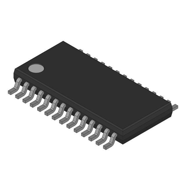
DW OR PW PACKAGE
(TOP VIEW)
Analog-to-Digital Converter (ADC)
D Low Power Consumption: 165 mW Typ
Using External references
D
D
D
D
D
D
D
Wide Analog Input Bandwidth: 700 MHz Typ
3.3 V Single-Supply Operation
3.3 V TTL/CMOS-Compatible Digital I/O
Internal Bottom and Top Reference Voltages
Adjustable Reference Input Range
Power Down (Standby) Mode
Separate Power Down for Internal Voltage
References
Three-State Outputs
D
D 28-Pin Small Outline IC (SOIC) and Thin
D
Shrink SOP (TSSOP) Packages
Applications
− Digital Communications
− Flat Panel Displays
− High-Speed DSP Front-End
(TMS320C6000)
− Medical Imaging
− Graphics Processing (Scan Rate/Format
Conversion)
− DVD Read Channel Digitization
DESCRIPTION
The TLV5580 is an 8-bit 80 MSPS high-speed A/D
converter. It converts the analog input signal into
8-bit binary-coded digital words up to a sampling
rate of 80 MHz. All digital inputs and outputs are
3.3 V TTL/CMOS-compatible.
The device consumes very little power due to the
3.3 V supply and an innovative single-pipeline
architecture implemented in a CMOS process.
The user obtains maximum flexibility by setting
both bottom and top voltage references from
user-supplied voltages. If no external references
are available, on-chip references are available for
DRVDD
D0
D1
D2
D3
D4
D5
D6
D7
DRVSS
DVSS
CLK
OE
DVDD
1
28
2
27
3
26
4
25
5
24
6
23
7
22
8
21
9
20
10
19
11
18
12
17
13
16
14
15
AVSS
AVDD
AIN
CML
PWDN_REF
AVSS
REFBO
REFBI
REFTI
REFTO
AVSS
BG
AVDD
STBY
internal and external use. The full-scale range is
1 Vpp up to 1.6 Vpp, depending on the analog
supply voltage. If external references are
available, the internal references can be disabled
independently from the rest of the chip, resulting
in an even greater power saving.
While usable in a wide variety of applications, the
device is specifically suited for the digitizing of
high-speed graphics and for interfacing to LCD
panels or LCD/DMD projection modules . Other
applications include DVD read channel
digitization,
medical
imaging
and
communications. This device is suitable for IF
sampling of communication systems using
sub-Nyquist sampling methods because of its
high analog input bandwidth.
Please be aware that an important notice concerning availability, standard warranty, and use in critical applications of
Texas Instruments semiconductor products and disclaimers thereto appears at the end of this data sheet.
All trademarks are the property of their respective owners.
Copyright 1999−2003, Texas Instruments Incorporated
������ �� ���� ����������� �! "#��$�� �! �� %#&'�"����� (��$)
��(#"�!
"������ �� !%$"���"�����! %$� �*$ �$��! �� �$+�! �!��#�$��! !���(��( ,������-)
��(#"���� %��"$!!��. (�$! ��� �$"$!!���'- ��"'#($ �$!���. �� �'' %����$�$�!)
www.ti.com
��������
��� �
�� ��
� ����
���� ��� ���������
www.ti.com
SLAS205B − DECEMBER 1998 − REVISED OCTOBER 2003
FUNCTIONAL BLOCK DIAGRAM
+
ADC
−
SHA
SHA
ADC
SHA
SHA
SHA
SHA
2
DAC
2
2
2
2
2
2
Correction Logic
Output Buffers
D0(LSB)−D7(MSB)
The single-pipeline architecture uses 6 ADC/DAC stages and one final flash ADC. Each stage produces a
resolution of 2 bits. The correction logic generates its result using the 2-bit result from the first stage, 1 bit from
each of the 5 succeeding stages, and 1 bit from the final stage in order to arrive at an 8-bit result. The correction
logic ensures no missing codes over the full operating temperature range.
PACKAGE/ORDERING INFORMATION
SPECIFIED
TEMPERATURE
RANGE
PACKAGE
MARKING
PRODUCT
PACKAGE−LEAD
PACKAGE
DESIGNATOR(1)
ORDERING
NUMBER
TLV5580
SOIC, 28
DW
0°C to +70°C
TLV5580C
TLV5580CDW
Rails, 20
″
″
″
″
″
TLV5580CDWR
Tape and Reel, 1000
TLV5580
TSSOP. 28
PW
0°C to +70°C
TV5580
TLV5580CPW
Rails, 20
″
″
″
″
″
TLV5580CPWR
Tape and Reel, 2000
TLV5580
SOIC, 28
DW
−40°C to +85°C
TLV5580I
TLV5580IDW
Rails, 50
″
″
″
″
″
TLV5580IDWR
Tape and Reel, 1000
TLV5580
TSSOP, 28
PW
−40°C to +85°C
TY5580
TLV5580IPW
Rails, 50
″
″
″
″
″
TLV5580IPWR
(1) For the most current specifications and package information, refer to our web site at www.ti.com.
2
TRANSPORT MEDIA,
QUANTITY
Tape and Reel, 2000
��������
��� �
�� ��
� ����
���� ��� ���������
www.ti.com
SLAS205B − DECEMBER 1998 − REVISED OCTOBER 2003
CIRCUIT DIAGRAMS OF INPUTS AND OUTPUTS
ALL DIGITAL INPUT CIRCUITS
AIN INPUT CIRCUIT
DVDD
AVDD
0.5 pF
REFERENCE INPUT CIRCUIT
AVDD
Internal
Reference
Generator
REFTO
or
REFBO
D0−D7 OUTPUT CIRCUIT
DRVDD
D
AVDD
D_Out
OE
REFBI
or
REFTI
DRVSS
3
��������
��� �
�� ��
� ����
���� ��� ���������
www.ti.com
SLAS205B − DECEMBER 1998 − REVISED OCTOBER 2003
Terminal Functions
TERMINAL
NAME
AIN
AVDD
AVSS
NO.
I/O
DESCRIPTION
26
I
Analog input
16, 27
I
Analog supply voltage
18, 23, 28
I
Analog ground
BG
17
O
Band gap reference voltage. A 1 µF capacitor (with an optional 0.1 µF capacitor in parallel) should be
connected between this terminal and AVSS for external filtering.
CLK
12
I
Clock input. The input is sampled on each rising edge of CLK.
CML
25
O
Common mode level. This voltage is equal to (AVDD − AVSS) ÷ 2. An external 0.1 µF capacitor should be
connected between this terminal and AVSS.
D0 − D7
2−9
O
Data outputs. D7 is the MSB
DRVDD
DRVSS
1
I
Supply voltage for digital output drivers
10
I
Ground for digital output drivers
DVDD
OE
14
I
Digital supply voltage
13
I
Output enable. When high the D0 − D7 outputs go in high-impedance mode.
DVSS
PWDN_REF
11
I
Digital ground
24
I
Power down for internal reference voltages. A high on this terminal will disable the internal reference circuit.
REFBI
21
I
Reference voltage bottom input. The voltage at this terminal defines the bottom reference voltage for the
ADC. It can be connected to REFBO or to an externally generated reference level. Sufficient filtering should
be applied to this input. The use a 0.1 µF capacitor connected between REFBI and AVSS is recommended.
Additionally, a 0.1 µF capacitor can be connected between REFTI and REFBI.
REFBO
22
O
Reference voltage bottom output. An internally generated reference is available at this terminal. It can be
connected to REFBI or left unconnected. A 1 µF capacitor between REFBO and AVSS will provide sufficient
decoupling required for this output.
REFTI
20
I
Reference voltage top input. The voltage at this terminal defines the top reference voltage for the ADC. It
can be connected to REFTO or to an externally generated reference level. Sufficient filtering should be
applied to this input. The use of a 0.1 µF capacitor between REFTI and AVSS is recommended. Additionally,
a 0.1 µF capacitor can be connected between REFTI and REFBI.
REFTO
19
O
Reference voltage top output. An internally generated reference is available at this terminal. It can be
connected to REFTI or left unconnected. A 1 µF capacitor between REFTO and AVSS will provide sufficient
decoupling required for this output.
STBY
15
I
Standby input. A high level on this input enables a power-down mode.
4
��������
��� �
�� ��
� ����
���� ��� ���������
www.ti.com
SLAS205B − DECEMBER 1998 − REVISED OCTOBER 2003
ABSOLUTE MAXIMUM RATINGS OVER OPERATING FREE-AIR TEMPERATURE (unless
otherwise noted)†
Supply voltage: AVDD to AGND, DVDD to DGND . . . . . . . . . . . . . . . . . . . . . . . . . . . . . . . . . . . . −0.5 V to 4.5 V
Supply voltage: AVDD to DVDD, AGND to DGND . . . . . . . . . . . . . . . . . . . . . . . . . . . . . . . . . . . . −0.5 V to 0.5 V
Digital input voltage range to DGND . . . . . . . . . . . . . . . . . . . . . . . . . . . . . . . . . . . . . . . . −0.5 V to DVDD + 0.5 V
Analog input voltage range to AGND . . . . . . . . . . . . . . . . . . . . . . . . . . . . . . . . . . . . . . . . −0.5 V to AVDD + 0.5 V
Digital output voltage applied from external source to DGND . . . . . . . . . . . . . . . . . . . −0.5 V to DVDD + 0.5 V
Reference voltage input range to AGND: V(REFTI), V(REFTO), V(REFBI), V(REFBO) −0.5 V to AVDD + 0.5 V
Operating free-air temperature range, TA: TLV5580C . . . . . . . . . . . . . . . . . . . . . . . . . . . . . . . . . . 0°C to 70°C
TLV5580I . . . . . . . . . . . . . . . . . . . . . . . . . . . . . . . . . −40°C to 85°C
Storage temperature range, Tstg . . . . . . . . . . . . . . . . . . . . . . . . . . . . . . . . . . . . . . . . . . . . . . . . . . −55°C to 150°C
(1) †Stresses beyond those listed under “absolute maximum ratings” may cause permanent damage to the device. These are stress ratings only, and
functional operation of the device at these or any other conditions beyond those indicated under “recommended operating conditions” is not
implied. Exposure to absolute-maximum-rated conditions for extended periods may affect device reliability.
RECOMMENDED OPERATING CONDITIONS OVER OPERATING FREE-TEMPERATURE RANGE
POWER SUPPLY
Supply voltage
AVDD
DVDD
MIN
NOM
MAX
3
3.3
3.6
UNIT
V
DRVDD
ANALOG AND REFERENCE INPUTS
Reference input voltage (top), V(REFTI)
Reference input voltage (bottom), V(REFBI)
MIN
NOM
MAX
UNIT
(NOM) − 0.2
2 + (AVDD − 3)
(NOM) + 0.2
V
0.8
1
Reference voltage differential, V(REFTI) − V(REFBI)
Analog input voltage, V(AIN)
1.2
V
1 + (AVDD − 3)
V
V(REFTI)
V
V(REFBI)
DIGITAL INPUTS
MIN
High-level input voltage, VIH
Low-level input voltage, VIL
2.0
DGND
NOM
MAX
UNIT
DVDD
0.2xDVDD
V
V
Clock period, tc
12.5
ns
Pulse duration, clock high, tw(CLKH)
5.25
ns
Pulse duration, clock low, tw(CLKL)
5.25
ns
5
��������
��� �
�� ��
� ����
���� ��� ���������
www.ti.com
SLAS205B − DECEMBER 1998 − REVISED OCTOBER 2003
ELECTRICAL CHARACTERISTICS OVER RECOMMENDED OPERATING CONDITIONS WITH FCLK = 80
MSPS AND USE OF EXTERNAL VOLTAGE REFERENCES (unless otherwise noted)
POWER SUPPLY
PARAMETER
IDD
Operating supply current
TEST CONDITIONS
AVDD
DVDD
DRVDD
PD
Power dissipation
PD(STBY)
Standby power
MIN
TYP
MAX
57
71
3
3.6
5
7.5
PWDN_REF = L
213
270
PWDN_REF = H
165
210
11
15
TYP
MAX
AVDD = DVDD = 3.3 V, DRVDD = 3 V,
CL = 15 pF, VI = 1 MHz, −1 dBFS
STBY = H,
CLK held high or low
UNIT
mA
mW
DIGITAL LOGIC INPUTS
PARAMETER
IIH
High-level input current on CLK†
IIL
Low-level input current on digital inputs
(OE, STDBY, PWDN_REF, CLK)
TEST CONDITIONS
MIN
AVDD = DVDD = DRVDD = CLK = 3.6 V
AVDD = DVDD = DRVDD = 3.6 V,
Digital inputs at 0 V
UNIT
10
µA
10
µA
CI
Input capacitance
5
pF
† IIH leakage current on other digital inputs (OE, STDBY, PWDN_REF) is not measured since these inputs have an internal pull-down resistor of
4 KΩ to DGND.
LOGIC OUTPUTS
PARAMETER
TEST CONDITIONS
VOH
High-level output voltage
AVDD = DVDD = DRVDD = 3 V at IOH = 50 µA,
Digital output forced high
VOL
Low-level output voltage
AVDD = DVDD = DRVDD = 3.6 V at IOL = 50 µA,
Digital output forced low
CO
Output capacitance
IOZH
High-impedance state output current to
high level
IOZL
6
High-impedance state output current to
low level
MIN
TYP
MAX
2.8
UNIT
V
0.1
5
V
pF
10
µA
10
µA
AVDD = DVDD = DRVDD = 3.6 V
��������
��� �
�� ��
� ����
���� ��� ���������
www.ti.com
SLAS205B − DECEMBER 1998 − REVISED OCTOBER 2003
ELECTRICAL CHARACTERISTICS OVER RECOMMENDED OPERATING CONDITIONS WITH FCLK = 80
MSPS AND USE OF EXTERNAL VOLTAGE REFERENCES (unless otherwise noted)
DC ACCURACY
PARAMETER
TEST CONDITIONS
Integral nonlinearity (INL), best-fit
Internal references (see Note 1)
Differential nonlinearity (DNL)
Internal references (see Note 2)
Zero error
TA = −40°C to 85°C
TA = −40°C to 85°C
AVDD = DVDD = 3.3 V, DRVDD = 3 V
Full scale error
MIN
TYP
MAX
UNIT
LSB
−2.4
±1
2.4
−1
± 0.6
1.3
LSB
5
%FS
5
%FS
See Note 3
1. Integral nonlinearity refers to the deviation of each individual code from a line drawn from zero to full scale. The point used as zero
occurs 1/2 LSB before the first code transition. The full−scale point is defined as a level 1/2 LSB beyond the last code transition. The deviation
is measured from the center of each particular code to the true straight line between these two endpoints.
2. An ideal ADC exhibits code transitions that are exactly 1 LSB apart. DNL is the deviation from this ideal value. Therefore this measure indicates
how uniform the transfer function step sizes are. The ideal step size is defined here as the step size for the device under test (i.e., (last transition
level − first transition level) ÷ (2n − 2)). Using this definition for DNL separates the effects of gain and offset error. A minimum DNL better than −1
LSB ensures no missing codes.
3. Zero error is defined as the difference in analog input voltage − between the ideal voltage and the actual voltage − that will switch the ADC output
from code 0 to code 1. The ideal voltage level is determined by adding the voltage corresponding to 1/2 LSB to the bottom reference level. The
voltage corresponding to 1 LSB is found from the difference of top and bottom references divided by the number of ADC output levels (256).
Full-scale error is defined as the difference in analog input voltage – between the ideal voltage and the actual voltage – that will switch the ADC
output from code 254 to code 255. The ideal voltage level is determined by subtracting the voltage corresponding to 1.5 LSB from the top reference
level. The voltage corresponding to 1 LSB is found from the difference of top and bottom references divided by the number of ADC output levels
(256).
ANALOG INPUT
PARAMETER
CI
TEST CONDITIONS
MIN
Input capacitance
TYP
MAX
4
UNIT
pF
REFERENCE INPUT (AVDD = DVDD = DRVDD = 3.6 V)
PARAMETER
Rref
Iref
TEST CONDITIONS
MIN
Reference input resistance
TYP
MAX
Reference input current
UNIT
Ω
200
5
mA
REFERENCE OUTPUTS
PARAMETER
V(REFTO)
V(REFBO)
Reference top offset voltage
Reference bottom offset voltage
TEST CONDITIONS
Absolute min/max values valid
and tested for AVDD = 3.3 V
MAX
UNIT
2.07
MIN
2 + [(AVDD − 3) ÷ 2]
TYP
2.21
V
1.09
1 + [(AVDD − 3) ÷ 2]
1.21
V
7
��������
��� �
�� ��
� ����
���� ��� ���������
www.ti.com
SLAS205B − DECEMBER 1998 − REVISED OCTOBER 2003
ELECTRICAL CHARACTERISTICS OVER RECOMMENDED OPERATING CONDITIONS WITH FCLK = 80
MSPS AND USE OF EXTERNAL VOLTAGE REFERENCES (unless otherwise noted) (continued)
DYNAMIC PERFORMANCE†
PARAMETER
Effective number of bits, ENOB
Signal-to-total harmonic distortion + noise, S/(THD+N)
Total harmonic distortion (THD)
Spurious free dynamic range (SFDR)
Analog input full-power bandwidth, BW
TEST CONDITIONS
fin = 1 MHz
fin = 4.43 MHz
MIN
TYP
6.2
6.7
6.2
6.7
fin = 15 MHz
fin = 76 MHz
fin = 1 MHz
fin = 4.43 MHz
6.4
39
42
39
42
40
fin = 15 MHz
fin = 76 MHz
See Note 4
Bits
dB
40
−46
−50
−45.5
−49
fin = 15 MHz
fin = 76 MHz
fin = 1 MHz
fin = 4.43 MHz
UNIT
6.5
fin = 15 MHz
fin = 76 MHz
fin = 1 MHz
fin = 4.43 MHz
MAX
−44
dB
−45.5
48
51
48
51
46
dB
48
700
MHz
0.8
°
fclk = 40 MHz, fin = 4.43 MHz,
20 IRE amplitude vs. full-scale of 140 IRE
Differential gain, DG
0.6
%
† Based on analog input voltage of − 1 dBFS referenced to a 1.3 Vpp full-scale input range and using the external voltage references at
fclk = 80 MSPS with AVDD = DVDD = 3.3 V and DRVDD = 3.0 V at 25°C.
4. The analog input bandwidth is defined as the maximum frequency of a −1 dBFS input sine that can be applied to the device for which an extra
3 dB attenuation is observed in the reconstructed output signal.
Differential phase, DP
8
��������
��� �
�� ��
� ����
���� ��� ���������
www.ti.com
SLAS205B − DECEMBER 1998 − REVISED OCTOBER 2003
ELECTRICAL CHARACTERISTICS OVER RECOMMENDED OPERATING CONDITIONS WITH FCLK = 80
MSPS AND USE OF EXTERNAL VOLTAGE REFERENCES (unless otherwise noted) (continued)
TIMING REQUIREMENTS
PARAMETER
TEST CONDITIONS
fclk
fclk
Maximum conversion rate
td(o)
th(o)
Output delay time (see Figure 1)
MIN
TYP
MAX
UNIT
80
MHz
Minimum conversion rate
CL = 10 pF,
CL = 2 pF,
Output hold time
td(pipe)
Pipeline delay (latency)
td(a)
tj(a)
Aperture delay time
tdis
ten
Disable time, OE rising to Hi-Z
See Notes 5 and 6
4.5
See Note 5
10
kHz
9
ns
2
See Note 6
ns
4.5
4.5
4.5
CLK
cycles
3
Aperture jitter
ns
1.5
See Note 5
Enable, OE falling to valid data
ps, rms
5
8
ns
5
8
ns
5. Output timing td(o) is measured from the 1.5 V level of the CLK input falling edge to the 10%/90% level of the digital output. The digital output load
is not higher than 10 pF.
Output hold time th(o) is measured from the 1.5 V level of the CLK input falling edge to the 10%/90% level of the digital output. The digital output
is load is not less than 2 pF.
Aperture delay td(A) is measured from the 1.5 V level of the CLK input to the actual sampling instant.
The OE signal is asynchronous.
OE timing tdis is measured from the VIH(MIN) level of OE to the high-impedance state of the output data. The digital output load is not higher than
10 pF.
OE timing ten is measured from the VIL(MAX) level of OE to the instant when the output data reaches VOH(min) or VOL(max) output levels. The digital
output load is not higher than 10 pF.
6. The number of clock cycles between conversion initiation on an input sample and the corresponding output data being made available from the
ADC pipeline. Once the data pipeline is full, new valid output data is provided on every clock cycle. In order to know when data is stable on the
output pins, the output delay time td(o) (i.e., the delay time through the digital output buffers) needs to be added to the pipeline latency. Note that
since the max. td(o) is more than 1/2 clock period at 80 MHz; data cannot be reliably clocked in on a rising edge of CLK at this speed. The falling
edge should be used.
N+3
N
N+1
N+2
tj(A)
N+5
N+4
td(A)
CLK
VIH
(min)
tw(CLKH)
tw(CLKL)
VIL
(max)
1.5 V
1.5 V
1/fCLK
td(o)
th(o)
D0−D7
N−4
N−3
N−2
VOH(min)
N−1
N
90%
N+1
10%
VOL(max)
tdis
td(pipe)
ten
VIH(min)
VIL(max)
OE
Figure 1. Timing Diagram
9
��������
��� �
�� ��
� ����
���� ��� ���������
www.ti.com
SLAS205B − DECEMBER 1998 − REVISED OCTOBER 2003
PERFORMANCE PLOTS AT 25°C
1
DNL − LSB
0.8
0.6
0.4
0.2
0
−0.2
−0.4
−0.6
−0.8
−1
0
50
100
150
200
250
ADC Code
Figure 2. DNL vs Input Code At 80 MSPS (With External Reference, PW Package)
2
1.5
INL − LSB
1
0.5
0
−0.5
−1
−1.5
−2
0
50
100
150
200
250
ADC Code
Figure 3. INL vs Input Code At 80 MSPS (With External Reference, PW Package)
10
��������
��� �
�� ��
� ����
���� ��� ���������
www.ti.com
SLAS205B − DECEMBER 1998 − REVISED OCTOBER 2003
PERFORMANCE PLOTS AT 25°C (Continued)
50
45
40
60 MSPS
40 MSPS
S(THD+N) − dB
35
80 MSPS
30
25
20
15
10
5
0
0
10
20
30
40
50
60
70
80
90 100
Analog Input Frequency − MHz
Figure 4. S/(THD+N) vs VIN At 80 MSPS (Internal Reference),
60 MSPS (External Reference), 40 MSPS (External Reference)
0
−10
Power − dBFS
−20
−30
−40
−50
−60
−70
−80
−90
0
5
10
15
20
25
30
f − Frequency − MHz
Figure 5. Spectral Plot fIN = 1.011 MHz At 60 MSPS
11
��������
��� �
�� ��
� ����
���� ��� ���������
www.ti.com
SLAS205B − DECEMBER 1998 − REVISED OCTOBER 2003
PERFORMANCE PLOTS AT 25°C (Continued)
0
−10
Power − dBFS
−20
−30
−40
−50
−60
−70
−80
−90
0
5
10
15
20
25
30
35
40
f − Frequency − MHz
Figure 6. Spectral Plot fIN = 0.996 MHz At 80MSPS
0
−10
Power − dBFS
−20
−30
−40
−50
−60
−70
−80
−90
0
5
10
15
20
25
30
35
40
35
40
f − Frequency − MHz
Figure 7. Spectral Plot fIN = 15.527 MHz At 80 MSPS
0
−10
Power − dBFS
−20
−30
−40
−50
−60
−70
−80
−90
0
5
10
15
20
25
30
f − Frequency − MHz
Figure 8. Spectral Plot fIN = 75.02 MHz At 80MSPS
(Plot shows folded spectrum of undersampled input signal)
12
��������
��� �
�� ��
� ����
���� ��� ���������
www.ti.com
SLAS205B − DECEMBER 1998 − REVISED OCTOBER 2003
PERFORMANCE PLOTS AT 25°C (Continued)
250
5
4.5
200
4
IDRVDD − mA
150
100
3
2.5
2
1.5
50
1
0.5
0
0
10
20
30
40
50
60
70
80
90 100
0
0
Sampling Frequency − MHz
10
20
30
40
50
60
70
80
90 100
Sampling Frequency − MHz
Figure 9. Power vs fCLK
At VIN = 1 MHz, −1 dBFS
Figure 10. IDRVDD vs fCLK
At VIN = 1 MHz, −1 dBFS
0
−1
Fundamental Power − dBFS
Power − mW
3.5
−2
−3
−4
−5
−6
−7
−8
−9
−10
106
107
108
Analog Input Frequency − Hz
109
Figure 11. ADC Output Power With Respect To −1 dBFS VIN
(Internal Reference, DW Package)
13
��������
��� �
�� ��
� ����
���� ��� ���������
www.ti.com
SLAS205B − DECEMBER 1998 − REVISED OCTOBER 2003
PRINCIPLE OF OPERATION
The TLV5580 implements a high-speed 80 MSPS converter in a cost-effective CMOS process. Powered from
3.3 V, the single-pipeline design architecture ensures low-power operation and 8 bit accuracy. Signal input and
clock signals are all single-ended. The digital inputs are 3.3 V TTL/ CMOS compatible. Internal voltage
references are included for both bottom and top voltages. Therefore the converter forms a self-contained
solution. Alternatively the user may apply externally generated reference voltages. In doing so, both input offset
and input range can be modified to suit the application.
A high-speed sampling-and-hold captures the analog input signal. Multiple stages will generate the output code
with a pipeline delay of 4.5 CLK cycles. Correction logic combines the multistage data and aligns the 8-bit output
word. All digital logic operates at the rising edge of CLK.
ANALOG INPUT
TLV5580
RS
AIN
S1
RSW
VS
CI
Figure 12. Simplified Equivalent Input Circuit
A first-order approximation for the equivalent analog input circuit of the TLV5580 is shown in Figure 12. The
equivalent input capacitance CI is 4 pF typical. The input must charge/discharge this capacitance within the
sample period of one half clock cycle. When a full-scale voltage step is applied, the input source provides the
charging current through the switch resistance RSW (200 Ω) of S1 and quickly settles. In this case the input
impedance is low. Alternatively, when the source voltage equals the value previously stored on CI, the hold
capacitor requires no input current and the equivalent input impedance is very high.
To maintain the frequency performance outlined in the specifications, the total source impedance should be
limited to about 80 Ω, as follows from the equation with fCLK = 80 MHz, CI = 4 pF, RSW = 200 Ω:
R
S
t
ƪ1 ÷ ǒ2fCLK
C
I
Ǔ
In(256) –R
ƫ
SW
So, for applications running at a lower fCLK, the total source resistance can increase proportionally.
14
��������
��� �
�� ��
� ����
���� ��� ���������
www.ti.com
SLAS205B − DECEMBER 1998 − REVISED OCTOBER 2003
PRINCIPLE OF OPERATION
DC COUPLED INPUT
REFTI
REFTI
RIN
REFTO
VIN
TLV5580
+
_
AIN
AVDD
RIN
VIN
REFTO
_
VREF
TLV5580
AIN
+
R1
REFBI
REFBI
REFBO
REFBO
R2
(b)
(a)
Figure 13. DC-Coupled Input Circuit
For dc-coupled systems an op amp can level-shift a ground-referenced input signal. A circuit as shown in
Figure 13(a) is acceptable. Alternatively, the user might want a bipolar shift together with the bottom reference
voltage as seen in Figure 13(b). In this case the AIN voltage is given by:
AIN + 2
ǒ
Ǔ
R ÷ R )R
2
2
1
V
REF
–V
IN
AC COUPLED INPUT
C1
TLV5580
R1
VIN
AIN
R2
C2
+
−
VBIAS
Figure 14. AC-Coupled Input Circuit
For many applications, especially in single supply operation, ac coupling offers a convenient way for biasing
the analog input signal at the proper signal range. Figure 14 shows a typical configuration. To maintain the
outlined specifications, the component values need to be carefully selected. The most important issue is the
positioning of the 3 dB high-pass corner point f−3 dB, which is a function of R2 and the parallel combination of
C1 and C2, called Ceq. This is given by the following equation:
f
–3 dB
ǒ
Ǔ
+ 1 ÷ 2π x R x C eq
2
where Ceq is the parallel combination of C1 and C2.
Since C1 is typically a large electrolytic or tantalum capacitor, the impedance becomes inductive at higher
frequencies. Adding a small ceramic or polystyrene capacitor, C2 of approximately 0.01 µF, which is not
inductive within the frequency range of interest, maintains low impedance. If the minimum expected input signal
frequency is 20 kHz, and R2 equals 1 kΩ and R1 equals 50 Ω, the parallel capacitance of C1 and C2 must be
a minimum of 8 nF to avoid attenuating signals close to 20 kHz.
15
��������
��� �
�� ��
� ����
���� ��� ���������
www.ti.com
SLAS205B − DECEMBER 1998 − REVISED OCTOBER 2003
PRINCIPLE OF OPERATION
REFERENCE TERMINALS
The voltages on terminals REFBI and REFTI determine the TLV5580’s input range. Since the device has an
internal voltage reference generator with outputs available on REFBO respectively REFTO, corresponding
terminals can be directly connected externally to provide a contained ADC solution. Especially at higher
sampling rates, it is advantageous to have a wider analog input range. The wider analog input range is
achievable by using external voltage references (e.g., at AVDD = 3.3 V, the full scale range can be extended
from 1 Vpp (internal reference) to 1.3 Vpp (external reference) as shown in Table 1). These voltages should
not be derived via a voltage divider from a power supply source. Instead, use a bandgap-derived voltage
reference to derive both references via an op amp circuit. Refer to the schematic of the TLV5580 evaluation
module for an example circuit.
When using external references, the full-scale ADC input range and its dc position can be adjusted. The
full-scale ADC range is always equal to VREFT – VREFB. The maximum full-scale range is dependent on AVDD
as shown in the specification section. In addition to the limitation on their difference, VREFT and VREFB each
also have limits on their useful range. These limits are also dependent on AVDD.
Table 3 summarizes these limits for 3 cases.
Table 1. Recommended Operating Modes
AVDD
3V
VREFB(min)
0.8 V
VREFB(max)
1.2 V
VREFT(min)
1.8 V
VREFT(max)
2.2 V
[VREFT−VREFB]max
1V
3.3 V
0.8 V
1.2 V
2.1 V
2.5 V
1.3 V
3.6 V
0.8 V
1.2 V
2.4 V
2.8 V
1.6 V
DIGITAL INPUTS
The digital inputs are CLK, STDBY, PWDN_REF, and OE. All these signals, except CLK, have an internal
pull-down resistor to connect to digital ground. This provides a default active operation mode using internal
references when left unconnected.
The CLK signal at high frequencies should be considered as an analog input. Overshoot/undershoot should
be minimized by proper termination of the signal close to the TLV5580. An important cause of performance
degradation for a high-speed ADC is clock jitter. Clock jitter causes uncertainty in the sampling instant of the
ADC, in addition to the inherent uncertainty on the sampling instant caused by the part itself, as specified by
its aperture jitter. There is a theoretical relationship between the frequency (f) and resolution (2N) of a signal
that needs to be sampled and the maximum amount of aperture error dtmax that is tolerable. The following
formula shows the relation:
ƪ
ƫ
dt max + 1 B p f 2 ǒN)1Ǔ
As an example, for an 8−bit converter with a 15-MHz input, the jitter needs to be kept